AP2315GEN
Halogen-Free Product
Advanced Power
Electronics Corp.
P-CHANNEL ENHANCEMENT MODE
POWER MOSFET
▼ Simple Drive Requirement
D
▼ Small Package Outline
▼ Surface Mount Device
S
▼ RoHS Compliant & Halogen Free
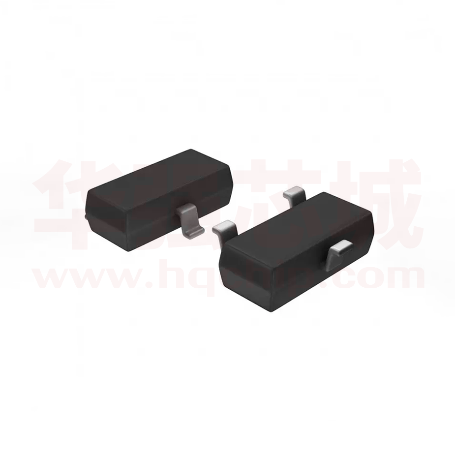
SOT-23S
BVDSS
-30V
RDS(ON)
1.25Ω
ID
- 840mA
G
D
Description
AP2315 series are from Advanced Power innovated design and silicon
process technology to achieve the lowest possible on-resistance and
fast switching performance. It provides the designer with an extreme
efficient device for use in a wide range of power applications.
The SOT-23S package is widely preferred for commercial-industrial
surface mount applications and suited for low voltage applications such
as DC/DC converters.
G
S
o
Absolute Maximum Ratings@Tj=25 C(unless otherwise specified)
Symbol
Parameter
.
Rating
Units
VDS
Drain-Source Voltage
- 30
V
VGS
Gate-Source Voltage
+16
V
-840
mA
-670
mA
-2.5
A
0.69
W
ID@TA=25℃
ID@TA=70℃
3
Drain Current , VGS @ 10V
3
Drain Current , VGS @ 10V
1
IDM
Pulsed Drain Current
PD@TA=25℃
Total Power Dissipation
TSTG
Storage Temperature Range
-55 to 150
℃
TJ
Operating Junction Temperature Range
-55 to 150
℃
Thermal Data
Symbol
Rthj-a
Parameter
3
Maximum Thermal Resistance, Junction-ambient
Data and specifications subject to change without notice
Value
Unit
180
℃/W
1
201411174AP
�AP2315GEN
Electrical Characteristics@Tj=25oC(unless otherwise specified)
Symbol
BVDSS
RDS(ON)
Parameter
Test Conditions
Drain-Source Breakdown Voltage
Static Drain-Source On-Resistance
2
Min.
Typ.
Max. Units
VGS=0V, ID=-250uA
-30
-
-
V
VGS=-10V, ID=-0.8A
-
-
1.25
Ω
VGS=-4.5V, ID=-0.5A
-
-
2.4
Ω
VGS(th)
Gate Threshold Voltage
VDS=VGS, ID=-250uA
-1
-
-3
V
gfs
Forward Transconductance
VDS=-10V, ID=-0.8A
-
880
-
mS
IDSS
Drain-Source Leakage Current
VDS=-30V, VGS=0V
-
-
-1
uA
IGSS
Gate-Source Leakage
VGS=+16V, VDS=0V
-
-
+30
uA
Qg
Total Gate Charge
ID=-0.8A
-
1
1.6
nC
Qgs
Gate-Source Charge
VDS=-25V
-
0.6
-
nC
Qgd
Gate-Drain ("Miller") Charge
VGS=-4.5V
-
0.4
-
nC
td(on)
Turn-on Delay Time
VDS=-15V
-
10
-
ns
tr
Rise Time
ID=-0.8A
-
8
-
ns
td(off)
Turn-off Delay Time
RG=3.3Ω
-
22
-
ns
tf
Fall Time
VGS=-10V
-
17
-
ns
Ciss
Input Capacitance
VGS=0V
-
30
50
pF
Coss
Output Capacitance
VDS=-25V
-
15
-
pF
Crss
Reverse Transfer Capacitance
f=1.0MHz
-
10
-
pF
Min.
Typ.
IS=-1.1A, VGS=0V
-
-
-1.3
V
.
Source-Drain Diode
Symbol
Parameter
2
Test Conditions
Max. Units
VSD
Forward On Voltage
trr
Reverse Recovery Time
IS=-0.8A, VGS=0V,
-
27
-
ns
Qrr
Reverse Recovery Charge
dI/dt=100A/µs
-
30
-
nC
Notes:
1.Pulse width limited by Max. junction temperature.
2.Pulse test
2
3.Surface mounted on 1 in copper pad of FR4 board, t < 10s ; 400℃/W when mounted on min. copper pad.
THIS PRODUCT IS SENSITIVE TO ELECTROSTATIC DISCHARGE, PLEASE HANDLE WITH CAUTION.
USE OF THIS PRODUCT AS A CRITICAL COMPONENT IN LIFE SUPPORT OR OTHER SIMILAR SYSTEMS IS NOT AUTHORIZED.
APEC DOES NOT ASSUME ANY LIABILITY ARISING OUT OF THE APPLICATION OR USE OF ANY PRODUCT OR CIRCUIT DESCRIBED
HEREIN; NEITHER DOES IT CONVEY ANY LICENSE UNDER ITS PATENT RIGHTS, NOR THE RIGHTS OF OTHERS.
APEC RESERVES THE RIGHT TO MAKE CHANGES WITHOUT FURTHER NOTICE TO ANY PRODUCTS HEREIN TO IMPROVE
RELIABILITY, FUNCTION OR DESIGN.
2
�AP2315GEN
2.0
2.0
-10V
-7.0V
-10V
TA=150oC
-ID , Drain Current (A)
-ID , Drain Current (A)
T A =25 o C
1.5
-5.0V
1.0
-4.5V
-7.0V
1.5
65mΩ
1.0
-5.0V
-4.5V
0.5
0.5
V G = -3.0V
V G = -3.0V
0.0
0.0
0
2
4
6
0
8
2
4
6
8
-V DS , Drain-to-Source Voltage (V)
-V DS , Drain-to-Source Voltage (V)
Fig 1. Typical Output Characteristics
Fig 2. Typical Output Characteristics
1.8
4.5
I D = -0.8A
V GS = -10V
I D = -0.5A
o
T A =25 C
1.6
2.5
.
Normalized RDS(ON)
RDS(ON) (mΩ )
3.5
1.4
1.2
1.0
1.5
0.8
0.5
0.6
2
4
6
8
10
-50
0
50
100
150
T j , Junction Temperature ( o C)
-V GS , Gate-to-Source Voltage (V)
Fig 3. On-Resistance v.s. Gate Voltage
Fig 4. Normalized On-Resistance
v.s. Junction Temperature
1.4
0.8
-IS(A)
T j =150 o C
Normalized VGS(th)
0.6
T j =25 o C
0.4
1.1
0.8
0.2
0.0
0.5
0
0.3
0.6
0.9
1.2
-V SD , Source-to-Drain Voltage (V)
Fig 5. Forward Characteristic of
Reverse Diode
1.5
-50
0
50
100
T j , Junction Temperature (
150
o
C)
Fig 6. Gate Threshold Voltage v.s.
Junction Temperature
3
�AP2315GEN
f=1.0MHz
100
8
I D = -0.8A
V DS = -25V
6
65mΩ
C (pF)
-VGS , Gate to Source Voltage (V)
10
C iss
4
2
C oss
C rss
10
0
0
0.5
1
1.5
2
2.5
1
3
5
9
13
17
21
25
29
-V DS , Drain-to-Source Voltage (V)
Q G , Total Gate Charge (nC)
Fig 7. Gate Charge Characteristics
Fig 8. Typical Capacitance Characteristics
1
Operation in this area
limited by RDS(ON)
100us
-ID (A)
1
.
1ms
10ms
0.1
100ms
o
T A =25 C
Single Pulse
1s
DC
1
10
Duty factor=0.5
0.2
0.1
PDM
0.1
t
0.05
T
0.02
Duty factor = t/T
Peak Tj = PDM x Rthja + T a
0.01
Rthja = 400℃/W
Single pulse
0.01
0.01
0.1
Normalized Thermal Response (Rthja)
10
100
0.0001
0.001
0.01
-V DS , Drain-to-Source Voltage (V)
0.1
1
10
100
1000
t , Pulse Width (s)
Fig 9. Maximum Safe Operating Area
Fig 10. Effective Transient Thermal Impedance
1.0
VG
V DS = -5V
-ID , Drain Current (A)
0.8
T j =25 o C
QG
T j =150 o C
-4.5V
0.6
QGS
QGD
0.4
0.2
Charge
Q
0.0
0
2
4
6
-V GS , Gate-to-Source Voltage (V)
Fig 11. Transfer Characteristics
Fig 12. Gate Charge Waveform
4
�AP2315GEN
MARKING INFORMATION
Part Number : NL
NLSS
Date Code : SS
SS:2004,2008,2012…
SS:2003,2007,2011…
SS:2002,2006,2010…
SS:2001,2005,2009…
.
5
�
很抱歉,暂时无法提供与“AP2315GEN”相匹配的价格&库存,您可以联系我们找货
免费人工找货- 国内价格
- 5+0.68726
- 50+0.49797
- 150+0.38566
- 500+0.34931
- 3000+0.32022
- 6000+0.30569
- 国内价格
- 1+0.74994
- 100+0.69995
- 300+0.64995
- 500+0.59995
- 2000+0.57496
- 5000+0.55996


 工商网监
湘ICP备2023018690号
工商网监
湘ICP备2023018690号


