GE
Data Sheet
MicroTLynxTM 12A: Non-Isolated DC-DC Power Modules
2.4Vdc –5.5Vdc input; 0.6Vdc to 3.63Vdc output; 12A Output Current
Features
▪
Compliant to RoHS Directive 2011/65/EU and amended
Directive (EU) 2015/863 (Z versions)
▪
Compatible in a Pb-free or SnPb reflow environment (Z
versions)
▪
Compliant to REACH Directive (EC) No 1907/2006
▪
Wide Input voltage range (2.4Vdc-5.5Vdc)
▪
Output voltage programmable from 0.6Vdc to 3.63 Vdc
via external resistor
▪
Tunable LoopTM to optimize dynamic output voltage
response
▪
Flexible output voltage sequencing EZ-SEQUENCE –
APTH versions
Applications
▪
Remote sense
▪
Distributed power architectures
▪
Fixed switching frequency
▪
Intermediate bus voltage applications
▪
Output overcurrent protection (non-latching)
▪
Telecommunications equipment
▪
Overtemperature protection
▪
Servers and storage applications
▪
Remote On/Off
▪
Networking equipment
▪
Ability to sink and source current
▪
Industrial equipment
▪
Cost efficient open frame design
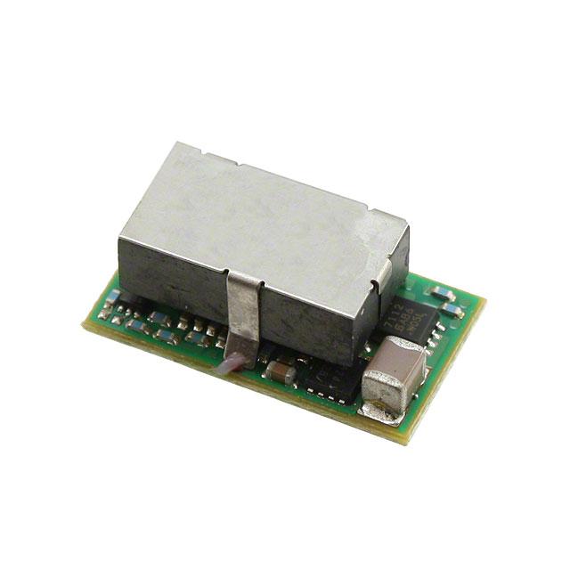
▪
Small size: 20.3 mm x 11.4 mm x 8.5 mm
RoHS Compliant
Vin+
VIN
EZ-SEQUENCETM
Vout+
VOUT
SENSE
MODULE
RTUNE
SEQ
Cin
CTUNE
Q1
ON/OFF
▪
Wide operating temperature range (-40°C to 85°C)
▪
ANSI/UL* 62368-1 and CAN/ CSA† C22.2 No. 62368-1
Recognized, DIN VDE‡ 0868-1/A11:2017 (EN623681:2014/A11:2017)
▪
ISO** 9001 and ISO 14001 certified manufacturing
facilities
Co
TRIM
GND
(0.8 in x 0.45 in x 0.334 in)
RTrim
Description
The Micro TLynxTM series of power modules are non-isolated dc-dc converters that can deliver up to 12A of output current.
These modules operate over a wide range of input voltage (VIN = 2.4Vdc-5.5Vdc) and provide a precisely regulated output
voltage from 0.6Vdc to 3.63Vdc, programmable via an external resistor. Features include remote On/Off, adjustable output
voltage, over current and overtemperature protection, and output voltage sequencing (APTH versions). A new feature, the
Tunable LoopTM, allows the user to optimize the dynamic response of the converter to match the load with reduced amount of
output capacitance leading to savings on cost and PWB area.
* UL is a registered trademark of Underwriters Laboratories, Inc.
†
CSA is a registered trademark of Canadian Standards Association.
VDE is a trademark of Verband Deutscher Elektrotechniker e.V.
** ISO is a registered trademark of the International Organization of Standards
‡
February 17, 2021
©2017 General Electric Corporation. All rights
reserved.
�GE
Data Sheet
MicroTLynxTM 12A: Non-Isolated DC-DC Power Modules
2.4Vdc –5.5Vdc input; 0.6Vdc to 3.63Vdc output; 12A Output Current
Absolute Maximum Ratings
Stresses in excess of the absolute maximum ratings can cause permanent damage to the device. These are absolute stress ratings only,
functional operation of the device is not implied at these or any other conditions in excess of those given in the operations sections of
the data sheet. Exposure to absolute maximum ratings for extended periods can adversely affect the device reliability.
Parameter
Input Voltage
Device
Symbol
Min
Max
Unit
All
VIN
-0.3
6
Vdc
APTH
VSEQ
-0.3
ViN, Max
Vdc
All
TA
-40
85
°C
All
Tstg
-55
125
°C
Continuous
Sequencing Voltage
Operating Ambient Temperature
(see Thermal Considerations section)
Storage Temperature
Electrical Specifications
Unless otherwise indicated, specifications apply over all operating input voltage, resistive load, and temperature conditions.
Parameter
Device
Symbol
Min
Typ
2.4
⎯
Max
Unit
Operating Input Voltage
All
VIN
Maximum Input Current
All
IIN,max
5.5
Vdc
11A
Adc
VO,set = 0.6 Vdc
IIN,No load
36
mA
VO,set = 3.3Vdc
IIN,No load
81
mA
All
IIN,stand-by
3
mA
Inrush Transient
All
I2t
Input Reflected Ripple Current, peak-to-peak
(5Hz to 20MHz, 1μH source impedance; VIN =0 to
5.5V, IO= IOmax ; See Test Configurations)
All
49
mAp-p
Input Ripple Rejection (120Hz)
All
-30
dB
(VIN=2.4V to 5.5V, IO=IO, max )
Input No Load Current
(VIN = 5.0Vdc, IO = 0, module enabled)
Input Stand-by Current
(VIN = 5.0Vdc, module disabled)
February 17, 2021
©2017 General Electric Corporation. All rights
reserved.
A2s
1
Page 2
�GE
Data Sheet
MicroTLynxTM 12A: Non-Isolated DC-DC Power Modules
2.4Vdc –5.5Vdc input; 0.6Vdc to 3.63Vdc output; 12A Output Current
Electrical Specifications (continued)
Parameter
Device
Symbol
Min
Output Voltage Set-point
All
VO, set
-1.5
Output Voltage
All
VO, set
-3.0
All
VO
0.6
Typ
⎯
Max
Unit
+1.5
% VO, set
+3.0
% VO, set
3.63
Vdc
(Over all operating input voltage, resistive load, and
temperature conditions until end of life)
Adjustment Range
Selected by an external resistor
Output Regulation (for VO ≥ 2.5Vdc)
Line (VIN=VIN, min to VIN, max)
All
⎯
0.4
% VO, set
Load (IO=IO, min to IO, max)
All
⎯
10
mV
Line (VIN=VIN, min to VIN, max)
All
⎯
10
mV
Load (IO=IO, min to IO, max)
All
⎯
5
mV
Temperature (Tref=TA, min to TA, max)
All
⎯
0.4
% VO, set
0.5
V
Output Regulation (for VO < 2.5Vdc)
Remote Sense Range
All
Output Ripple and Noise on nominal output
(VIN=VIN, nom and IO=IO, min to IO, max Co = 0.1μF // 10 μF
ceramic capacitors)
Peak-to-Peak (5Hz to 20MHz bandwidth)
All
⎯
25
35
mVpk-pk
RMS (5Hz to 20MHz bandwidth)
All
⎯
10
15
mVrms
1
External Capacitance
Without the Tunable LoopTM
All
CO, max
0
⎯
200
μF
ESR ≥ 0.15 mΩ
All
CO, max
0
⎯
1000
μF
ESR ≥ 10 mΩ
All
CO, max
0
⎯
5000
μF
Output Current
All
Io
0
Output Current Limit Inception (Hiccup Mode )
All
IO, lim
Output Short-Circuit Current
All
IO, s/c
30
% Io,max
ESR ≥ 1 mΩ
With the Tunable LoopTM
12
Adc
200
% Io,max
(VO≤250mV) ( Hiccup Mode )
Efficiency
VO,set = 0.6Vdc
η
75.0
%
VIN= 3.3Vdc, TA=25°C
VO, set = 1.2Vdc
η
85.5
%
IO=IO, max , VO= VO,set
VO,set = 1.8Vdc
η
89.9
%
VO,set = 2.5Vdc
η
92.7
%
Vin=5Vdc
Switching Frequency
VO,set = 3.3Vdc
η
All
fsw
94.6
⎯
600
%
⎯
kHz
1
External capacitors may require using the new Tunable LoopTM feature to ensure that the module is stable as well as getting the best transient
response. See the Tunable LoopTM section for details.
February 17, 2021
©2017 General Electric Corporation. All rights
reserved.
Page 3
�GE
Data Sheet
MicroTLynxTM 12A: Non-Isolated DC-DC Power Modules
2.4Vdc –5.5Vdc input; 0.6Vdc to 3.63Vdc output; 12A Output Current
General Specifications
Parameter
Min
Typ
Calculated MTBF (IO=IO, max, TA=25°C) Telecordia Issue 2, Method 1 Case 3
Max
Unit
28,160,677
⎯
Weight
Hours
⎯
3.59 (0.127)
g (oz.)
Feature Specifications
Unless otherwise indicated, specifications apply over all operating input voltage, resistive load, and temperature conditions. See
Feature Descriptions for additional information.
Parameter
Device
Symbol
Min
Typ
Max
Unit
All
All
IIH
VIH
⎯
VIN – 0.8
⎯
⎯
10
VIN,max
µA
V
All
All
IIL
VIL
⎯
-0.2
⎯
⎯
0.3
0.3
mA
V
Input High Current
All
IIH
―
―
2
mA
Input High Voltage
All
VIH
VIN – 1.6
―
VIN, max
Vdc
On/Off Signal Interface
(VIN=VIN, min to VIN, max ; open collector or equivalent,
Signal referenced to GND)
Device is with suffix “4” – Positive Logic (See Ordering
Information)
Logic High (Module ON)
Input High Current
Input High Voltage
Logic Low (Module OFF)
Input Low Current
Input Low Voltage
Device Code with no suffix – Negative Logic (See Ordering
Information)
(On/OFF pin is open collector/drain logic input with
external pull-up resistor; signal referenced to GND)
Logic High (Module OFF)
Logic Low (Module ON)
Input low Current
All
IIL
―
―
1
mA
Input Low Voltage
All
VIL
-0.2
―
VIN – 1.6
Vdc
All
Tdelay
―
2
―
msec
All
Tdelay
―
2
―
msec
All
Trise
―
5
―
msec
3.0
% VO, set
Turn-On Delay and Rise Times
(VIN=VIN, nom, IO=IO, max , VO to within ±1% of steady state)
Case 1: On/Off input is enabled and then input power is
applied (delay from instant at which VIN = VIN, min until
Vo = 10% of Vo, set)
Case 2: Input power is applied for at least one second
and then the On/Off input is enabled (delay from instant
at which Von/Off is enabled until Vo = 10% of Vo, set)
Output voltage Rise time (time for Vo to rise from
10% of Vo, set to 90% of Vo, set)
Output voltage overshoot (TA = 25oC
VIN= VIN, min to VIN, max,IO = IO, min to IO, max)
With or without maximum external capacitance
Over Temperature Protection
All
Tref
(See Thermal Considerations section)
Sequencing Delay time
Delay from VIN, min to application of voltage on SEQ pin
130
°C
APTH
TsEQ-delay
Tracking Accuracy
(Power-Up: 2V/ms)
APTHl
VSEQ –Vo
100
mV
(Power-Down: 2V/ms)
APTH
VSEQ –Vo
100
mV
10
msec
(VIN, min to VIN, max; IO, min to IO, max VSEQ < Vo)
February 17, 2021
©2017 General Electric Corporation. All rights
reserved.
Page 4
�GE
Data Sheet
MicroTLynxTM 12A: Non-Isolated DC-DC Power Modules
2.4Vdc –5.5Vdc input; 0.6Vdc to 3.63Vdc output; 12A Output Current
Feature Specifications (continued)
Parameter
Device
Symbol
Min
Typ
Max
Units
2.2
Vdc
Input Undervoltage Lockout
Turn-on Threshold
All
Turn-off Threshold
All
1.75
Hysteresis
All
0.08
February 17, 2021
©2017 General Electric Corporation. All rights
reserved.
Vdc
0.2
Vdc
Page 5
�GE
Data Sheet
MicroTLynxTM 12A: Non-Isolated DC-DC Power Modules
2.4Vdc –5.5Vdc input; 0.6Vdc to 3.63Vdc output; 12A Output Current
Characteristic Curves
The following figures provide typical characteristics for the Micro TLynxTM at 0.6Vo and at 25oC.
90
13
12
OUTPUT CURRENT, Io (A)
EFFICIENCY, (%)
85
80
Vin=2.4V
75
Vin=3.3V
Vin=5.5V
70
0
2
4
6
8
10
11
NC
8
25
12
February 17, 2021
55
65
75
VO (V) (200mV/div)
IO (A) (5Adiv)
OUTPUT CURRENT,
OUTPUT VOLTAGE
Figure 5. Typical Start-up Using On/Off Voltage (Io = Io,max).
45
Figure 2. Derating Output Current versus Ambient Temperature
and Airflow.
TIME, t (20s /div)
VO (V) (200mV/div)
Figure 4. Transient Response to Dynamic Load Change from 0%
to 50% to 0% with VIN=5V.
INPUT VOLTAGE
TIME, t (1ms/div)
35
AMBIENT TEMPERATURE, TA OC
OUTPUT VOLTAGE
VO (V) (200mV/div)
VON/OFF (V) (2V/div)
ON/OFF VOLTAGE
OUTPUT VOLTAGE
Figure 3. Typical output ripple and noise (VIN = 5V, Io = Io,max).
0.5m/s
(100LFM)
9
VIN (V) (2V/div)
VO (V) (10mV/div)
OUTPUT VOLTAGE
TIME, t (1s/div)
1m/s
(200LFM)
10
OUTPUT CURRENT, IO (A)
Figure 1. Converter Efficiency versus Output Current.
2m/s
(400LFM)
TIME, t (1ms/div)
Figure 6. Typical Start-up Using Input Voltage (VIN = 5V, Io =
Io,max).
©2017 General Electric Corporation. All rights
reserved.
Page 6
85
�GE
Data Sheet
MicroTLynxTM 12A: Non-Isolated DC-DC Power Modules
2.4Vdc –5.5Vdc input; 0.6Vdc to 3.63Vdc output; 12A Output Current
Characteristic Curves (continued)
95
13
90
12
OUTPUT CURRENT, Io (A)
EFFICIENCY, (%)
The following figures provide typical characteristics for the Micro TLynxTM at 1.2Vo and at 25oC.
85
Vin=2.4V
Vin=3.3V
Vin=5.5V
80
75
70
11
2m/s
(400LFM)
1m/s
(200LFM)
10
0.5m/s
(100LFM)
9
NC
8
0
2
4
6
8
10
12
25
February 17, 2021
85
VO (V) (200mV/div)
IO (A) (5Adiv)
OUTPUT CURRENT,
OUTPUT VOLTAGE
Figure 11. Typical Start-up Using On/Off Voltage (Io = Io,max).
75
TIME, t (20s /div)
VO (V) (500mV/div)
Figure 10. Transient Response to Dynamic Load Change from
0% to 50% to 0% with VIN=5V.
INPUT VOLTAGE
TIME, t (1ms/div)
65
AMBIENT TEMPERATURE, TA C
OUTPUT VOLTAGE
VO (V) (500mV/div)
VON/OFF (V) (2V/div)
ON/OFF VOLTAGE
OUTPUT VOLTAGE
Figure 9. Typical output ripple and noise (VIN = 5V, Io = Io,max).
55
Figure 8. Derating Output Current versus Ambient
Temperature and Airflow.
VIN (V) (2V/div)
VO (V) (10mV/div)
OUTPUT VOLTAGE
TIME, t (1s/div)
45
O
OUTPUT CURRENT, IO (A)
Figure 7. Converter Efficiency versus Output Current.
35
TIME, t (1ms/div)
Figure 12. Typical Start-up Using Input Voltage (VIN = 5V, Io =
Io,max).
©2017 General Electric Corporation. All rights
reserved.
Page 7
�GE
Data Sheet
MicroTLynxTM 12A: Non-Isolated DC-DC Power Modules
2.4Vdc –5.5Vdc input; 0.6Vdc to 3.63Vdc output; 12A Output Current
Characteristic Curves (continued)
The following figures provide typical characteristics for the Micro TLynxTM at 1.8Vo and at 25oC.
13
100
12
OUTPUT CURRENT, Io (A)
EFFICIENCY, (%)
95
90
85
Vin=2.4V
Vin=3.3V Vin=5.5V
80
75
70
11
2m/s
(400LFM)
1m/s
(200LFM)
10
0.5m/s
(100LFM)
9
NC
8
0
2
4
6
8
10
12
25
February 17, 2021
85
VO (V) (200mV/div)
IO (A) (2Adiv)
OUTPUT CURRENT,
OUTPUT VOLTAGE
Figure 17. Typical Start-up Using On/Off Voltage (Io = Io,max).
75
VO (V) (1V/div)
Figure 16. Transient Response to Dynamic Load Change from
0% to 50% to 0% with VIN=5V.
OUTPUT VOLTAGE
TIME, t (1ms/div)
65
TIME, t (20s /div)
VIN (V) (2V/div)
VO (V) (500mV/div)
VON/OFF (V) (2V/div)
ON/OFF VOLTAGE OUTPUT VOLTAGE
Figure 15. Typical output ripple and noise (VIN = 5V, Io = Io,max).
55
Figure 14. Derating Output Current versus Ambient
Temperature and Airflow.
INPUT VOLTAGE
VO (V) (10mV/div)
OUTPUT VOLTAGE
TIME, t (1s/div)
45
AMBIENT TEMPERATURE, TA OC
OUTPUT CURRENT, IO (A)
Figure 13. Converter Efficiency versus Output Current.
35
TIME, t (1ms/div)
Figure 18. Typical Start-up Using Input Voltage (VIN = 5V, Io =
Io,max).
©2017 General Electric Corporation. All rights
reserved.
Page 8
�GE
Data Sheet
MicroTLynxTM 12A: Non-Isolated DC-DC Power Modules
2.4Vdc –5.5Vdc input; 0.6Vdc to 3.63Vdc output; 12A Output Current
Characteristic Curves (continued)
The following figures provide typical characteristics for the Micro TLynxTM at 2.5Vo and at 25oC.
13
100
12
90
Vin=5.5V
OUTPUT CURRENT, Io (A)
EFFICIENCY, (%)
95
Vin=3V
Vin=3.3V
85
80
11
2m/s
(400LFM)
10
0.5m/s
(100LFM)
9
NC
8
0
2
4
6
8
10
12
25
February 17, 2021
85
VO (V) (200mV/div)
IO (A) (5Adiv)
OUTPUT CURRENT,
OUTPUT VOLTAGE
Figure 23. Typical Start-up Using On/Off Voltage (Io = Io,max).
75
Figure 22. Transient Response to Dynamic Load Change from
0% to 50% to 0% with VIN=5V.
VO (V) (1V/div)
TIME, t (1ms/div)
65
TIME, t (20s /div)
OUTPUT VOLTAGE
VON/OFF (V) (5V/div)
VO (V) (1V/div)
Figure 21. Typical output ripple and noise (VIN = 5V, Io = Io,max).
55
AMBIENT TEMPERATURE, TA C
VIN (V) (2V/div)
TIME, t (1s/div)
45
Figure 20. Derating Output Current versus Ambient
Temperature and Airflow.
INPUT VOLTAGE
VO (V) (0mV/div)
OUTPUT VOLTAGE
Figure 19. Converter Efficiency versus Output Current.
35
O
OUTPUT CURRENT, IO (A)
ON/OFF VOLTAGE OUTPUT VOLTAGE
1m/s
(200LFM)
TIME, t (1ms/div)
Figure 24. Typical Start-up Using Input Voltage (VIN = 5V, Io =
Io,max).
©2017 General Electric Corporation. All rights
reserved.
Page 9
�GE
Data Sheet
MicroTLynxTM 12A: Non-Isolated DC-DC Power Modules
2.4Vdc –5.5Vdc input; 0.6Vdc to 3.63Vdc output; 12A Output Current
Characteristic Curves (continued)
The following figures provide typical characteristics for the Micro TLynxTM at 3.3Vo and at 25oC.
13
100
12
OUTPUT CURRENT, Io (A)
EFFICIENCY, (%)
95
Vin=5V
Vin=5.5V
Vin=4.5V
90
85
80
11
2m/s
(400LFM)
10
0.5m/s
(100LFM)
NC
9
8
0
2
4
6
8
10
12
25
February 17, 2021
85
VO (V) (200mV/div)
IO (A) (5Adiv)
OUTPUT CURRENT,
OUTPUT VOLTAGE
Figure 29. Typical Start-up Using On/Off Voltage (Io = Io,max).
75
Figure 28. Transient Response to Dynamic Load Change from
0% 50% to 0% with VIN=5V.
VO (V) (1V/div)
TIME, t (1ms/div)
65
TIME, t (20s /div)
OUTPUT VOLTAGE
VON/OFF (V) (2V/div)
VO (V) (1V/div)
Figure 27. Typical output ripple and noise (VIN = 5V, Io = Io,max).
55
AMBIENT TEMPERATURE, TA C
VIN (V) (2V/div)
TIME, t (1s/div)
45
Figure 26. Derating Output Current versus Ambient
Temperature and Airflow.
INPUT VOLTAGE
VO (V) (10mV/div)
OUTPUT VOLTAGE
Figure 25. Converter Efficiency versus Output Current.
35
O
OUTPUT CURRENT, IO (A)
ON/OFF VOLTAGE OUTPUT VOLTAGE
1m/s
(200LFM)
TIME, t (1ms/div)
Figure 30. Typical Start-up Using Input Voltage (VIN = 5V, Io =
Io,max).
©2017 General Electric Corporation. All rights
reserved.
Page 10
�GE
Data Sheet
MicroTLynxTM 12A: Non-Isolated DC-DC Power Modules
2.4Vdc –5.5Vdc input; 0.6Vdc to 3.63Vdc output; 12A Output Current
Test Configurations
Design Considerations
Input Filtering
CURRENT PROBE
The Micro TLynxTM module should be connected to a low acimpedance source. A highly inductive source can affect the
stability of the module. An input capacitance must be placed
directly adjacent to the input pin of the module, to minimize input
ripple voltage and ensure module stability.
LTEST
VIN(+)
BATTERY
1μH
CIN
CS 1000μF
Electrolytic
2x100μF
Tantalum
E.S.R.


 工商网监
湘ICP备2023018690号
工商网监
湘ICP备2023018690号
