1PMT4614e3 – 1PMT4627e3,
1PMT4099e3 – 1PMT4135e3
Powermite Low Noise
1 Watt Zener Diodes
Compliant
DESCRIPTION
This Microsemi Powermite surface mount low noise Zener package series provides a higher
power handling capability that are also RoHS compliant. In addition to its size advantages,
Powermite package features include a full-metallic bottom that eliminates the possibility of
solder flux entrapment during assembly, and a unique locking tab acts as an efficient heat path
from die to mounting plane for external heat sinking with very low thermal resistance junction
to case (bottom). Its innovative design makes this device ideal for use with automatic insertion
equipment.
Important: For the latest information, visit our website http://www.microsemi.com.
FEATURES
•
•
•
•
•
•
•
Surface mount equivalent to JEDEC registered 1N4099 through 1N4135 and 1N4614 through
1N4627 series except with additional power capability.
Extensive selection from 1.8 to 100 volts.
Regulates voltage over a broad operating current and temperature range.
Low R ӨJC for cooler operation and better voltage regulation.
Low noise density (1-3 kHz) at test current.
Low reverse leakage current.
RoHS compliant by design.
Also available in:
DO-35 package
(axial-leaded)
1N4099 – 1N4135 and
1N4614 – 1N4627
DO-213AA package
APPLICATIONS / BENEFITS
•
•
•
•
•
DO-216 Package
(surface mount)
1N4099UR – 1N4135UR and
1N4614UR – 1N4627UR
Tight tolerances available in plus or minus 2%.
Moisture classification Level 1 per IPC/JEDEC J-STD-020B with no dry pack required.
Non-sensitive to ESD per MIL-STD-750 method 1020.
Compatible with automatic insertion equipment.
Full metallic bottom eliminates flux entrapment.
MAXIMUM RATINGS
Parameters/Test Conditions
Junction and Storage Temperature
(1)
Thermal Resistance Junction-to-Ambient
Thermal Resistance Junction-to-Case
(2)
Steady-State Power Dissipation
Forward Voltage @ 200 mA
Solder Temperature @ 10 s
Notes: 1.
2.
Symbol
Value
TJ and TSTG
R ӨJA
R ӨJC
PD
VF
TSP
-55 to +150
240
30
1.0
1.1
260
Unit
o
C
C/W
o
C/W
W
V
o
C
o
On FR4 PC board (1 oz copper) with recommended footprint (see last page).
At T C < 120 oC where T C is case bottom temperature at mounting plane, or 0.5 watts at T A = 30 ºC
(ambient temperature) when mounted on FR4 PC board as described for R ӨJA (also see power
deratings in figure 2).
MSC – Lawrence
6 Lake Street,
Lawrence, MA 01841
Tel: 1-800-446-1158 or
(978) 620-2600
Fax: (978) 689-0803
MSC – Ireland
Gort Road Business Park,
Ennis, Co. Clare, Ireland
Tel: +353 (0) 65 6840044
Fax: +353 (0) 65 6822298
Website:
www.microsemi.com
RF01097, Rev. A (2/21/13)
©2013 Microsemi Corporation
Page 1 of 5
�1PMT4614e3 – 1PMT4627e3,
1PMT4099e3 – 1PMT4135e3
MECHANICAL and PACKAGING
•
•
•
•
•
•
•
CASE: Void-free transfer molded thermosetting epoxy compound meeting UL94V-0.
FINISH: Annealed matte-tin plating over copper and readily solderable per MIL-STD-750 method 2026. (Consult factory for tinlead plating. NOTE: Tin-lead plated product is not RoHS compliant.)
POLARITY: Cathode designated by Tab 1 (bottom).
TAPE AND REEL option: Standard per EIA-481-B (consult factory for quantities).
MARKING: Three numerical digits of P/N and a dot (see electrical characteristics).
WEIGHT: Approximately 0.016 grams.
See package dimensions on last page.
PART NOMENCLATURE
1
PMT 4099
C
e3
1 Watt
RoHS Compliance
Powermite Class
Zener Voltage Tolerance
Blank = 5%
C = 2%
JEDEC type number
(See Electrical Characteristics
table)
SYMBOLS & DEFINITIONS
Definition
Symbol
IR
I Z, I ZT, I ZK
I ZM
ND
VR
VZ
Z ZT or Z ZK
Reverse Current: The maximum reverse (leakage) current that will flow at the specified voltage and temperature.
Regulator Current: The dc regulator current (I Z), at a specified test point (I ZT), near breakdown knee (I ZK ).
Maximum Regulator (Zener) Current: The maximum rated dc current for the specified power rating.
Noise Density: The noise generated over a specified frequency bandwidth usually specified in terms of mV/ √Hz.
Reverse Voltage: The reverse voltage dc value, no alternating component.
Zener Voltage: The Zener voltage the device will exhibit at a specified current (I Z) in its breakdown region.
Dynamic Impedance: The small signal impedance of the diode when biased to operate in its breakdown region at a
specified rms current modulation (typically 10% of I ZT or I ZK ) and superimposed on I ZT or I ZK respectively.
RF01097, Rev. A (2/21/13)
©2013 Microsemi Corporation
Page 2 of 5
�1PMT4614e3 – 1PMT4627e3,
1PMT4099e3 – 1PMT4135e3
ELECTRICAL CHARACTERISTICS @ 25 °C unless otherwise stated
PART
NUMBER
(Note 4)
1PMT4614
1PMT4615
1PMT4616
1PMT4617
1PMT4618
1PMT4619
1PMT4620
1PMT4621
1PMT4622
1PMT4623
1PMT4624
1PMT4625
1PMT4626
1PMT4627
1PMT4099
1PMT4100
1PMT4101
1PMT4102
1PMT4103
1PMT4104
1PMT4105
1PMT4106
1PMT4107
1PMT4108
1PMT4109
1PMT4110
1PMT4111
1PMT4112
1PMT4113
1PMT4114
1PMT4115
1PMT4116
1PMT4117
1PMT4118
1PMT4119
1PMT4120
1PMT4121
1PMT4122
1PMT4123
1PMT4124
1PMT4125
1PMT4126
1PMT4127
1PMT4128
1PMT4129
1PMT4130
1PMT4131
1PMT4132
1PMT4133
1PMT4134
1PMT4135
NOMINAL
ZENER
VOLTAGE
DEVICE
(Note 1)
MARKING
V Z @ I ZT
614•
615•
616•
617•
618•
619•
620•
621•
622•
623•
624•
625•
626•
627•
099•
100•
101•
102•
103•
104•
105•
106•
107•
108•
109•
110•
111•
112•
113•
114•
115•
116•
117•
118•
119•
120•
121•
122•
123•
124•
125•
126•
127•
128•
129•
130•
131•
132•
133•
134•
135•
I ZT
MAXIMUM
ZENER
IMPEDANCE
(Note 2)
Z ZT
Volts
µA
Ohms
µA
Volts
µV/√HZ
mA
MAXIMUM
TEMPERATURE
COEFFICIENT
OF ZENER
VOLTAGE
α VZ
%/°C
1.8
2.0
2.2
2.4
2.7
3.0
3.3
3.6
3.9
4.3
4.7
5.1
5.6
6.2
6.8
7.5
8.2
8.7
9.1
10
11
12
13
14
15
16
17
18
19
20
22
24
25
27
28
30
33
36
39
43
47
51
56
60
62
68
75
82
87
91
100
250
250
250
250
250
250
250
250
250
250
250
250
250
250
250
250
250
250
250
250
250
250
250
250
250
250
250
250
250
250
250
250
250
250
250
250
250
250
250
250
250
250
250
250
250
250
250
250
250
250
250
1200
1250
1300
1400
1500
1600
1650
1700
1650
1650
1600
1500
1400
1200
200
200
200
200
200
200
200
200
200
200
100
100
100
100
150
150
150
150
150
150
200
200
200
200
200
250
250
300
300
400
500
700
700
800
1000
1200
1500
10
5.0
4.0
2.0
1.0
0.8
7.5
7.5
5.0
4.0
10
10
10
10
10
10
1
1
1
1
.05
.05
.05
.05
.05
.05
.05
.05
.05
.01
.01
.01
.01
.01
.01
.01
.01
.01
.01
.01
.01
.01
.01
.01
.01
.01
.01
.01
.01
.01
.01
1.0
1.0
1.0
1.0
1.0
1.0
1.5
2.0
2.0
2.0
3.0
3.0
4.0
5.0
5.17
5.70
6.24
6.61
6.92
7.60
8.44
9.12
9.87
10.65
11.40
12.15
12.92
13.37
14.44
15.20
16.72
18.25
19.00
20.45
21.28
22.80
25.08
27.38
29.65
32.65
35.75
38.76
42.60
45.60
47.10
51.68
57.00
62.32
66.12
69.16
76.00
1
1
1
1
1
1
1
1
1
1
1
2
4
5
40
40
40
40
40
40
40
40
40
40
40
40
40
40
40
40
40
40
40
40
40
40
40
40
40
40
40
40
40
40
40
40
40
40
40
40
40
262.4
240.6
218.7
207.8
196.8
190.3
185.9
181.5
174.9
168.4
164.0
153.1
142.2
133.4
122.5
111.5
100.6
96.2
91.9
83.1
76.5
69.9
63.4
59.0
54.8
52.5
48.1
45.9
43.7
41.6
37.2
34.9
32.8
30.6
30.6
28.4
26.2
24.0
21.4
19.5
17.7
16.4
14.7
13.9
13.3
12.2
11.2
10.1
9.6
9.2
8.3
-0.075
-0.075
-0.075
-0.075
-0.075
-0.075
-0.075
-0.065
-0.060
-0.050
-0.040 +0.020
-0.045 +0.030
-0.020 +0.040
-0.010 +0.050
0.040
0.045
0.048
0.049
0.050
0.055
0.060
0.065
0.065
0.070
0.070
0.070
0.075
0.075
0.075
0.075
0.080
0.080
0.080
0.085
0.085
0.085
0.085
0.090
0.090
0.090
0.090
0.090
0.090
0.090
0.090
0.095
0.095
0.095
0.095
0.095
0.095
ZENER
TEST
CURRENT
MAXIMUM
REVERSE
CURRENT
MAXIMUM
NOISE
DENSITY
IR @ V R
N D @ I ZT
MAXIMUM
ZENER
CURRENT
(Note 3)
I ZM
NOTE 1: Product shown has a standard tolerance of ± 5% on the nominal Zener voltage. V Z is measured at I ZT with Tc (TAB 1) at 30 °C.
NOTE 2: Zener impedance is derived by superimposing on I ZT a 60 Hz rms ac current equal to 10% of I ZT (25 µA ac).
NOTE 3: Based on 1 W maximum power dissipation before any derating. Allowance has been made for higher voltage with operation at higher
currents and temperature. For determination of voltage change with current deviations from I ZT see MicroNote 202.
RF01097, Rev. A (2/21/13)
©2013 Microsemi Corporation
Page 3 of 5
�1PMT4614e3 – 1PMT4627e3,
1PMT4099e3 – 1PMT4135e3
PD Rated Power Dissipation (mW)
GRAPHS
Temperature (oC)
FIGURE 2 - Power Derating Curve
Where TC is case (bottom) temperature and
TA is Ambient Temperature on FR4 PC board.
FIGURE 1 – Noise Density Measurement Circuit
Typical Capacitance in Picofarads (pF)
Noise density, (N D ) is specified in microvolt-rms per
square-root-hertz. Actual measurement is performed
using a 1 kHz to 3 kHz frequency bandpass filter at a
o
constant Zener test current (I ZT ) at 25 C ambient
temperature. N D is calculated from the formula.
Zener Voltage V Z
FIGURE 3 – Capacitance vs. Zener Voltage (Typical)
RF01097, Rev. A (2/21/13)
©2013 Microsemi Corporation
Page 4 of 5
�1PMT4614e3 – 1PMT4627e3,
1PMT4099e3 – 1PMT4135e3
PACKAGE DIMENSIONS
Ltr
A
B
C
D
E
F
G
H
J
K
Dimensions
Inch
Millimeters
Min
Max
Min
Max
0.029 0.039
0.73
0.99
0.016 0.026
0.40
0.66
0.070 0.080
1.77
2.03
0.087 0.097
2.21
2.46
0.020 0.030
0.50
0.76
0.051 0.061
1.29
1.54
0.021 0.031
0.53
0.78
0.004 0.008
0.10
0.20
0.070 0.080
1.77
2.03
0.035 0.045
0.89
1.14
PAD LAYOUT
Ltr
A
B
C
D
E
RF01097, Rev. A (2/21/13)
©2013 Microsemi Corporation
Dimensions
Inch
Millimeters
0.100
2.54
0.105
2.67
0.050
1.27
0.030
0.76
0.025
0.64
Page 5 of 5
�
很抱歉,暂时无法提供与“1PMT4104/TR7”相匹配的价格&库存,您可以联系我们找货
免费人工找货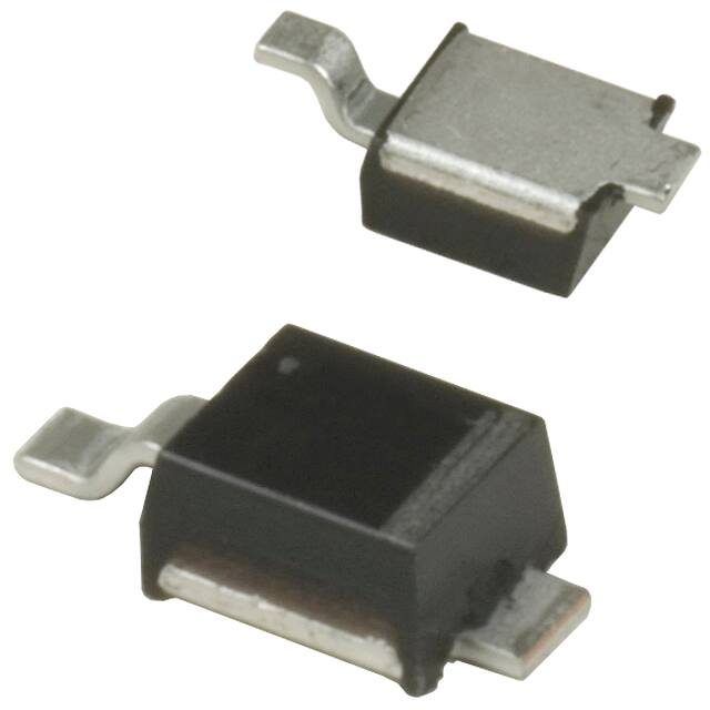


 工商网监
湘ICP备2023018690号
工商网监
湘ICP备2023018690号
