2N6317 and 2N6318
PNP SILICON POWER TRANSISTOR
Available
DESCRIPTION
These 2N6317 and 2N6318 devices are an excellent choice for un-tuned amplifier
applications. It is also ideal for general purpose power switch and amplifier applications.
Microsemi also offers numerous other products to meet higher and lower power voltage
regulation applications.
TO-213AA (TO-66)
Package
Important: For the latest information, visit our website http://www.microsemi.com.
FEATURES
•
•
•
Hermetically sealed.
Complimentary pairing with the NPN 2N6315 and 2N6316.
RoHS compliant versions available.
APPLICATIONS / BENEFITS
•
•
•
Convenient package.
Mechanically rugged.
Commercial, industrial, and military uses.
MAXIMUM RATINGS @ 25 ºC unless otherwise stated
Parameters/Test Conditions
Junction and Storage Temperature
(1)
Thermal Resistance Junction-to-Lead
Collector-Base Voltage
Emitter-Base Voltage
Collector-Emitter Voltage
Continuous Operating Collector Current
Continuous Base Current
(2)
Total Power Dissipation
2N6317
2N6318
2N6317
2N6318
Symbol
TJ and TSTG
RӨJL
VCBO
VEBO
VCEO
IC
PT
Value
-65 to +200
235
60
80
5
60
80
7
2
90
NOTES: 1. At 1/8 inch from case for 10 seconds.
2. Derate linearly at 0.515 W/ºC.
T4-LDS-0283, Rev. 1 (121659)
Unit
o
C
o
C
V
V
V
A
A
W
MSC – Lawrence
6 Lake Street,
Lawrence, MA 01841
Tel: 1-800-446-1158 or
(978) 620-2600
Fax: (978) 689-0803
MSC – Ireland
Gort Road Business Park,
Ennis, Co. Clare, Ireland
Tel: +353 (0) 65 6840044
Fax: +353 (0) 65 6822298
Website:
www.microsemi.com
©2012 Microsemi Corporation
Page 1 of 5
�2N6317 and 2N6318
MECHANICAL and PACKAGING
•
•
•
•
•
CASE: Hermetic, TO-66 package. Nickel plate with nickel cap.
TERMINALS: Solder dipped (Sn63/Pb37) over nickel plated alloy 52. RoHS compliant matte-tin plating is also available.
MARKING: MSC, part number, date code, polarity symbol.
WEIGHT: Approximately 5.7 grams.
See Package Dimensions on last page.
PART NOMENCLATURE
2N6317
(e3)
JEDEC Type Number
See Electrical Characteristics
table
SYMBOLS & DEFINITIONS
Definition
Symbol
IB
TC
VCB
VCC
VEB
RoHS Compliance
e3 = RoHS compliant
Blank = non-RoHS compliant
Base current
Case temperature
Collector-base voltage
Collector-supply voltage
Emitter-base voltage
T4-LDS-0283, Rev. 1 (121659)
©2012 Microsemi Corporation
Page 2 of 5
�2N6317 and 2N6318
ELECTRICAL CHARACTERISTICS @ 25 ºC unless otherwise stated
Parameters / Test Conditions
STATIC CHARACTERISTICS
Collector Cutoff Current
VCE = 60 VBE = 1.5 V, TC = 150 ºC
VCE = 80 VBE = 1.5 V, TC = 150 ºC
Collector Cutoff Current
VCE = 60 VBE = 1.5 V
VCE = 80 VBE = 1.5 V
Emitter Cutoff Current
VEB = 5 V
(1)
Collector-Emitter Open Base Sustain Voltage
IB = 0, IC = 100 mA
Collector Cutoff Current, Base Open
IB = 0, VCE = 30 V
IB = 0, VCE = 40 V
(1)
DC Forward Current Transfer Ratio
IC = 7 A, VCE = 4 V
IC = 2.5 A, VCE = 4 V
IC = 0.5 A, VCE = 4 V
(1)
Collector-Emitter Saturation Voltage
IC = 7.0 A, IB = 1.75 A
IC = 4.0 A, IB = 0.4 A
(1)
Base-Emitter Saturation Voltage
IC = 7.0 A, IB = 1.75 A
Symbol
Min.
Max.
Unit
2N6317
2N6318
ICEX
2.0
mA
2N6317
2N6318
ICEX
0.25
mA
IEBO
1.0
mA
0.5
mA
2N6317
2N6318
2N6317
2N6318
VCEO(sus)
60
80
ICEO
hFE
4
25
35
125
VCE(sat)
2.0
1.0
V
VBE(sat)
2.5
V
VBE
1.5
V
Max.
Unit
300
pF
Max.
Unit
tr
0.7
µs
ts
1.0
µs
tf
0.8
µs
(1)
Base-Emitter Voltage
IC = 2.5 A, VCE = 4.0 V
NOTE: 1. Pulse Width < 300 µs; duty cycle < 2 %.
DYNAMIC CHARACTERISTICS
Parameters / Test Conditions
Magnitude of Common Emitter Small-Signal
Short-Circuit Forward Current Transfer Ratio
VCE = 10 V, IC = 0.25 A, f = 1 MHz
Common Base Output
VCB = 10 V, IE = 0 A, f = 1 MHz
Common Emitter Small-Signal Short-Circuit
Forward Current Trans-Ratio
VCE = 4 V, IC = 0.5 A, f = 1 kHz
Symbol
Min.
|hfe|
4
Cob
hfe
20
Symbol
Min.
SWITCHING CHARACTERISTICS
Parameters / Test Conditions
Rise time
VCC = 30 V, IC = 25 A, IB1 = IB2 = 0.25 A (see figure 2)
Storage time
VCC = 30 V, IC = 25 A, IB1 = IB2 = 0.25 A (see figure 2)
Fall time
VCC = 30 V, IC = 25 A, IB1 = IB2 = 0.25 A (see figure 2)
T4-LDS-0283, Rev. 1 (121659)
©2012 Microsemi Corporation
Page 3 of 5
�2N6317 and 2N6318
IC, COLLECTOR CURRENT (AMPS)
GRAPHS
VCE, COLLECTOR-EMITTER VOLTAGE (VOLTS)
Figure 1
Safe Operating Area (TC = 25 ºC)
Figure 2
Switching Times Test Circuit
T4-LDS-0283, Rev. 1 (121659)
©2012 Microsemi Corporation
Page 4 of 5
�2N6317 and 2N6318
PACKAGE DIMENSIONS
DIM
A1
A2
B
C
D
E
F
G
H
J
K
L
M
N
T1
T2
Case
T4-LDS-0283, Rev. 1 (121659)
INCH
MIN
MAX
.470
.500
.620
.050
.075
.050
.360
.028
.034
.145 radius
.958
.962
.570
.590
.093
.107
.190
.210
.350 radius
.142
.152
.250
.340
MILLIMETERS
MIN
MAX
11.94
12.70
15.75
1.27
1.91
1.27
9.14
0.71
0.86
3.68 radius
24.33
24.43
14.48
14.99
2.36
2.72
4.83
5.33
8.89 radius
3.61
3.86
6.35
8.64
Base
Emitter
Collector
©2012 Microsemi Corporation
Page 5 of 5
�
很抱歉,暂时无法提供与“2N6317”相匹配的价格&库存,您可以联系我们找货
免费人工找货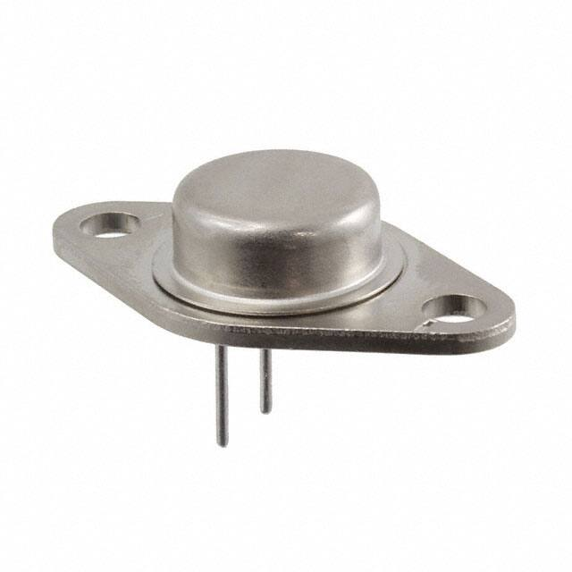


 工商网监
湘ICP备2023018690号
工商网监
湘ICP备2023018690号
