21130F.book Page 1 Wednesday, December 5, 2012 2:47 PM
Not recommended for new designs –
Please use 93AA76C or 93AA86C.
93AA76/86
8K/16K 1.8V Microwire Serial EEPROM
Features:
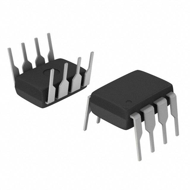
PDIP Package
1
2
3
4
8
VCC
7
6
5
PE
ORG
93AA76/86
CS
CLK
DI
DO
93AA76/86
• Single supply operation down to 1.8V
• Low-power CMOS technology:
- 1 mA active current typical
- 5 A standby current (typical) at 3.0V
• ORG pin selectable memory configuration:
- 1024 x 8 or 512 x 16-bit organization
(93AA76)
- 2048 x 8 or 1024 x 16-bit organization
(93AA86)
• Self-timed erase and write cycles
• Automatic ERAL before WRAL
• Power on/off data protection circuitry
• Industry standard 3-wire serial I/O
• Device status signal during erase/write cycles
• Sequential read function
• 1,000,000 erase/write cycles ensured
• Data retention > 200 years
• 8-pin PDIP/SOIC package
• Temperature ranges available:
- Commercial (C): 0C to +70C
Package Types
8
VSS
SOIC Package
CS
CLK
DI
DO
1
2
3
4
7
6
5
VCC
PE
ORG
VSS
Block Diagram
VCC VSS
Description:
The Microchip Technology Inc. 93AA76/86 are 8K and
16K low voltage serial Electrically Erasable PROMs.
The device memory is configured as x8 or x16 bits
depending on the ORG pin setup. Advanced CMOS
technology makes these devices ideal for low power
nonvolatile memory applications. These devices also
have a Program Enable (PE) pin to allow the user to
write-protect the entire contents of the memory array.
The 93AA76/86 is available in standard 8-pin PDIP and
8-pin surface mount SOIC packages.
Memory
Array
Address
Decoder
Address
Counter
Data
Register
Output
Buffer
DO
DI
PE
CS
CLK
1996-2012 Microchip Technology Inc.
Mode
Decode
Logic
Clock
Generator
DS21130F-page 1
�21130F.book Page 2 Wednesday, December 5, 2012 2:47 PM
93AA76/86
1.0
ELECTRICAL CHARACTERISTICS
Absolute Maximum Ratings(†)
VCC .............................................................................................................................................................................7.0V
All inputs and outputs w.r.t. VSS ........................................................................................................ -0.6V to Vcc + 1.0V
Storage temperature ...............................................................................................................................-65°C to +150°C
Ambient temperature with power applied ................................................................................................-40°C to +125°C
Soldering temperature of leads (10 seconds) .......................................................................................................+300°C
ESD protection on all pins ..........................................................................................................................................4 kV
† NOTICE: Stresses above those listed under “Absolute Maximum Ratings” may cause permanent damage to the
device. This is a stress rating only and functional operation of the device at these or any other conditions above those
indicated in the operational listings of this specification is not implied. Exposure to Absolute Maximum Rating
conditions for extended periods may affect device reliability.
1.1
AC Test Conditions
AC Waveform:
VLO = 2.0V
VHI = Vcc - 0.2V
(Note 1)
VHI = 4.0V for
(Note 2)
Timing Measurement Reference Level:
Input
0.5 VCC
Output
Note 1:
2:
0.5 VCC
For VCC 4.0V
For VCC 4.0V
DS21130F-page 2
1996-2012 Microchip Technology Inc.
�21130F.book Page 3 Wednesday, December 5, 2012 2:47 PM
93AA76/86
TABLE 1-1:
DC CHARACTERISTICS
DC CHARACTERISTICS
Parameter
Applicable over recommended operating ranges shown below unless otherwise noted:
VCC = +1.8V to +6.0V
Commercial (C): TA = 0°C to +70°C
Symbol
Min.
Max.
Units
Conditions
VCC 2.7V
VIH1
2.0
VCC + 1
V
VIH2
0.7 VCC
VCC + 1
V
VCC < 2.7V
Low-level input voltage
VIL1
-0.3
0.8
V
VCC 2.7V
VIL2
-0.3
0.2 VCC
V
VCC < 2.7V
Low-level output voltage
VOL1
—
0.4
V
IOL = 2.1 mA; VCC = 4.5V
VOL2
—
0.2
V
IOL =100 A; VCC = VCC Min.
High-level output voltage
VOH1
2.4
—
V
IOH = -400 A; VCC = 4.5V
VOH2
VCC-0.2
—
V
IOH = -100 A; VCC = VCC Min.
Input leakage current
ILI
-10
10
A
VIN = 0.1V to VCC
Output leakage current
ILO
-10
10
A
VOUT = 0.1V to VCC
Pin capacitance
(all inputs/outputs)
CINT
—
7
pF
(Note 1)
TA = +25°C, FCLK = 1 MHz
Operating current
ICC write
—
3
mA
VCC = 5.5V
ICC read
—
1
500
mA
A
FCLK = 3 MHz; VCC = 5.5V
FCLK = 1 MHz; VCC = 3.0V
ICCS
—
100
30
A
A
CLK = CS = 0V; VCC = 5.5V
CLK = CS = 0V; VCC = 3.0V
DI = PE = VSS
ORG = VSS or VCC
High-level input voltage
Standby current
Note 1:
This parameter is periodically sampled and not 100% tested.
1996-2012 Microchip Technology Inc.
DS21130F-page 3
�21130F.book Page 4 Wednesday, December 5, 2012 2:47 PM
93AA76/86
TABLE 1-2:
AC CHARACTERISTICS
AC CHARACTERISTICS
Parameter
Applicable over recommended operating ranges shown below unless otherwise noted:
VCC = +1.8V to +6.0V
Commercial (C): TA = 0°C to +70°C
Symbol
Min.
Max.
Units
Clock frequency
FCLK
—
3
2
1
MHz
MHz
Mhz
4.5V VCC 6.0V
2.5V VCC 4.5V
1.8V VCC 2.5V
Clock high time
TCKH
200
300
500
—
ns
ns
ns
4.5V VCC 6.0V
2.5V VCC 4.5V
1.8V VCC 2.5V
Clock low time
TCKL
100
200
500
—
ns
ns
ns
4.5V VCC 6.0V
2.5V VCC 4.5V
1.8V VCC < 2.5V
Chip select setup time
TCSS
50
100
250
—
ns
ns
ns
4.5V VCC 6.0V, Relative to CLK
2.5V VCC 4.5V, Relative to CLK
1.8V VCC 2.5V, Relative to CLK
Chip select hold time
TCSH
0
—
ns
1.8V VCC 6.0V
Chip select low time
TCSL
250
—
ns
1.8V VCC 6.0V, Relative to CLK
Data input setup time
TDIS
50
100
250
—
ns
ns
ns
4.5V VCC 6.0V, Relative to CLK
2.5V VCC
很抱歉,暂时无法提供与“93AA76/P”相匹配的价格&库存,您可以联系我们找货
免费人工找货