Atmel AT42QT1481
48-Key QMatrix FMEA IEC/EN60730 Touch Sensor IC
DATASHEET
Features
Number of keys:
Up to 48
Technology:
Patented charge-transfer (transverse mode), with frequency hopping
Key outline sizes:
6 mm × 6 mm or larger (panel thickness dependent); widely different sizes and
shapes possible
Key spacings:
8 mm or wider, center to center (panel thickness dependent)
Electrode design:
Two-part electrode shapes (drive-receive); wide variety of possible layouts
Layers required:
One layer (with jumpers), two layers (no jumpers)
Electrode materials:
PCB, FPCB, silver or carbon on film, ITO on film
Panel materials:
Plastic, glass, composites, painted surfaces (low particle density metallic
paints possible)
Adjacent Metal:
Compatible with grounded metal immediately next to keys
Panel thickness:
Up to 50 mm glass, 20 mm plastic (key size dependent)
Key sensitivity:
Individually settable via simple commands over serial interface
Signal processing:
Self-calibration, auto drift compensation, noise filtering, Adjacent Key
Suppression®
Interfaces:
UART
SPI slave (4 MHz maximum clock rate)
STATUS indication pin
Debug output
FMEA compliant design features
IEC/EN/UL60730 compliant design features
UL approval
VDE compliance
For use in both class B and class C safety-critical products
9621EX–AT42–07/2014
� Detects and Reports Key Failure
Power:
+4.75 to 5.25 V
Package:
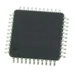
44-pin 10 × 10 mm TQFP RoHS compliant
AT42QT1481 [DATASHEET]
9621EX–AT42–07/2014
2
�44 43 42
Y4A
Y4B
Y5B
Y5A
VSS
VDD
Pinout Configuration
DRDY
STATUS / DBG_DATA
1.1
VREF
Pinout and Schematic
SS
S_SYNC / DBG_CLK
1.
MOSI
1
41 40 39 38 37 36 35 34
33
Y3B
MISO
2
32
Y2B
SCK
3
31
Y1B
4
30
Y0B
5
29
VDD
VSS
6
28
VSS
XT2
7
27
VDD
XT1
8
26
X7
RX
9
25
X6
TX
10
24
X5
23
21 22
X4
X2
X1
X0
VSS
VDD
Y0A
Y2A
Y1A
Y3A
11
12 13 14 15 16 17 18 19 20
SMP
WS
QT1481
X3
RST
VDD
AT42QT1481 [DATASHEET]
9621EX–AT42–07/2014
3
�1.2
Pin Descriptions
Table 1-1.
Pin Listing
Pin
Name
Type
Description
If Unused...
1
MOSI
I
SPI data input
Leave open
2
MISO
O
SPI data output
Leave open
3
SCK
I
SPI clock input
Vdd
4
RST
I
Reset low; has internal 30 k – 60 k pull-up resistor.
This pin should be controlled by the host.
Vdd
5
VDD
P
Power
–
6
VSS
P
Ground
–
7
XT2
O
8
XT1
I
9
RX
I
UART receive data input
Vdd
10
TX
O
UART transmit data; has internal 20 k – 50 k
pull-up resistor
Leave open
11
WS
I
Wake-up from sleep input and/or sync input
Vdd
12
SMP
I/O
Sample output
–
13
Y3A
I/O
Y line connection
Leave open
14
Y2A
I/O
Y line connection
Leave open
15
Y1A
I/O
Y line connection
Leave open
16
Y0A
I/O
Y line connection
Leave open
17
VDD
P
Power
–
18
VSS
P
Ground
–
19
X0
O
X matrix drive line
Leave open
20
X1
O
X matrix drive line
Leave open
21
X2
O
X matrix drive line
Leave open
22
X3
O
X matrix drive line
Leave open
23
X4
O
X matrix drive line
Leave open
24
X5
O
X matrix drive line
Leave open
25
X6
O
X matrix drive line
Leave open
26
X7
O
X matrix drive line/
Leave open
27
VDD
P
Power
–
28
VSS
P
Ground
–
29
VDD
P
Power
–
30
Y0B
I/O
Y line connection
Leave open
–
Ceramic resonator or crystal,16 MHz
–
AT42QT1481 [DATASHEET]
9621EX–AT42–07/2014
4
�Table 1-1.
Pin Listing (Continued)
Pin
Name
Type
Description
If Unused...
31
Y1B
I/O
Y line connection
Leave open
32
Y2B
I/O
Y line connection
Leave open
33
Y3B
I/O
Y line connection
Leave open
34
Y4A
I/O
Y line connection
Leave open
35
Y4B
I/O
Y line connection
Leave open
36
Y5A
I/O
Y line connection
Leave open
37
Y5B
I/O
Y line connection
Leave open
38
VDD
P
Power
–
39
VSS
P
Ground
–
40
STATUS /
DBG_DATA
O
Status output (active low) or Debug Data; has internal
20 k – 50 k pull-up resistor
Leave open
This pin MUST be used.
I
OD
1 = comms ready; needs a 100 µs grace period
before checking. Open-drain with internal 20 k –
50 k pull-up resistor
–
I
Connect to Vss
–
S_SYNC /
DBG_CLK
O
Scope Synchronization output or Debug Clock
Leave open
SS
I
SPI slave select; has internal 20 k – 50 k pull-up
resistor
Leave open
41
DRDY
I/O
42
VREF
43
44
Input only
Open drain output
O
P
Output only, push-pull
Ground or power
I/O
Input/output
AT42QT1481 [DATASHEET]
9621EX–AT42–07/2014
5
�1.3
Schematic
Figure 1-1. Typical Circuit
Vunreg
C2
SPI
38
S_SYNC /
DBG_CLK
SS
MISO
SCLK
3
Rx
9
Tx
10
SCK
RX
TX
QT1481
X4
23
X3
22
X2
21
X1
20
X0
19
Y0A
16
Y1B
DRDY
VDD
41
40
4.7k
8
DRDY
Y2A
STATUS /
DBG_DATA
Y2B
Y3A
XT1
Y3B
18
28
Y4B
VSS
VSS
VSS
Y5A
42
39
VSS
SMP
6
Y4A
Y5B
X6
Rx5
X5
Rx4
X4
Rx3
X3
Rx2
X2
Rx1
X1
Rx0
X0
Ry0
Y0
Cs0
30
Ry1
15
Y1
Cs1
31
Ry2
14
Y2
Cs2
32
Ry3
13
Y3
Cs3
33
Ry4
34
Y4
Cs4
35
Ry5
36
Y5
Cs5
37
12
Ceramic resonator
or crystal,16 MHz
XT2
VREF
7
X7
Rx6
25
24
Y1A
Rx7
26
X5
Y0B
11 WS
WAKE
SYNC
VDD
29
27
X6
1 MOSI
2 MISO
MOSI
X7
MATRIX X-DRIVE
44
SS
UART
43
RST
MATRIX Y-SCAN
4
SCOPE
17
C1
VDD
Creg2
C3
VDD
Creg1
5
+
VDD
+
VDD
VDD
VREG
Rs5 Rs4 Rs3 Rs2 Rs1 Rs0
For component values in Figure 1-1 check the following sections:
Section 2.7 on page 10: Cs capacitors (Cs0 – Cs5)
Section 2.8 on page 11: Sample resistors (Rs0 – Rs5)
Section 2.10 on page 12: Matrix resistors (Rx0 – Rx7, Ry0 – Ry5)
Section 2.13 on page 14: Power Supply
AT42QT1481 [DATASHEET]
9621EX–AT42–07/2014
6
�2.
Hardware and Functional
2.1
Introduction
The AT42QT1481 (QT1481) is a digital burst mode sensor, designed specifically for QMatrix layout touch controls; it
includes all signal processing functions necessary to provide stable sensing under a wide variety of changing
conditions. Only a few external parts are required for operation. The entire circuit can be built within a few square
centimeters of single-sided PCB area. CEM-1 and FR1 punched, single-sided materials can be used for the lowest
possible cost. The PCB’s rear can be mounted flush on the back of a glass or plastic panel using a conventional
adhesive, such as 3M VHB two-sided adhesive acrylic film.
The QT1481 employs transverse charge-transfer (QT™) sensing, a technology that senses changes in electrical
charge forced across two electrode elements by a pulse edge (see Figure 2-1).
Figure 2-1. Field Flow Between X and Y Elements
overlying panel
X element
Y element
CMOS
driver
The QT1481 allows a wide range of key sizes and shapes to be mixed together in a single touch panel. The QT1481
is designed for use with up to 48 keys.
The QT1481 uses both UART and SPI interfaces (only one at a time) to allow key data to be extracted and to permit
individual key parameter setup. The interface protocol uses simple single byte commands and responds with single
byte responses in most cases. The command structure is designed to minimize the amount of data traffic while
maximizing the amount of information conveyed.
In addition to normal operating and setup functions the QT1481 can also report back actual signal strengths and
error codes.
QmBtn software for the PC can be used to program the operation of the IC as well as read back key status and
signal levels in real time.
A Debug output interface is also supported, which can be used to monitor many operating variables during product
development.
The QT1481 incorporates many tests and checks to enable a product to achieve FMEA and EN60730 compliance.
The results of some tests need to be checked by the host. To achieve a compliant design, the host must read back
the test results and confirm their validity.
The QT1481 is able to scan the touch matrix twice as fast as previous generation devices; it can take twice the
number of samples in a given time frame. This mean s the QT1481 is much better equipped to continue normal
operation in the face of heavy noise.
See Appendix C. on page 68 for information on conducted noise immunity.
AT42QT1481 [DATASHEET]
9621EX–AT42–07/2014
7
�2.2
Key Numbers
The keys are numbered from 0 – 47.Table 2-1 shows the key numbering.
Table 2-1.
Key Numbers
X7
2.3
X6
X5
X4
X3
X2
X1
X0
Y0
7
6
5
4
3
2
1
0
Y1
15
14
13
12
11
10
9
8
Y2
23
22
21
20
19
18
17
16
Y3
31
30
29
28
27
26
25
24
Y4
39
38
37
36
35
34
33
32
Y5
47
46
45
44
43
42
41
40
Key
numbers
Matrix Scan Sequence
Key scanning begins with location X = 0, Y = 0 (key 0). All keys on X0 are scanned first, then X1 and finishing with all
keys on X7 (for example, the sequence X0Y0, X0Y1 – X0Y5, X1Y0, X1Y1...). Table 2-1 shows the key numbering.
All keys on the same X line are excited together in a burst of acquisition pulses whose length is determined by the
Setups parameter BL (see Section 5.9 on page 43); this can be set to a different value for each k ey. A burst is
completed entirely before the next X line is excited. At the end of each burst the resulting signals, one for each Y line,
are converted to digital form and processed. The burst length directly impacts key gain. Each key can have a
different burst length in order to allow tailoring of key sensitivity. Although all keys on an entire X line are excited
simultaneously, the charge is selectively captured at each Y line according to the burst length selected.
2.4
Enabling/Disabling Keys – Burst Paring
Unused keys are always pared from the computation sequence in order to optimize speed. If all keys are disabled on
any given X, the entire X line is also pared from the burst sequence. If only two X lines have enabled keys, only two
timeslots are used for scanning.
The NDIL parameter is used to enable and disable keys in the matrix. Setting NDIL = 0 for a key disables it (Section
5.5 on page 41). Keys that are disabled are eliminated from the scan sequence to save scan time and thus power. If
all keys on an X line are disabled, the burst for the entire X line is removed from the scan sequence, further saving
time and power. This has the consequence of affecting the scan rate of the entire matrix as well as the time required
for initial matrix calibration. It does not affect the time required to calibrate an individual key once the matrix is initially
calibrated after power-up or reset.
It is very important that only those keys that physically exist are enabled. All non-existent k eys must be disabled
(NDIL = 0) otherwise other keys in the matrix can incorrectly report their signal as zero.
AT42QT1481 [DATASHEET]
9621EX–AT42–07/2014
8
�2.5
Response Time
The response time of the QT1481 depends on:
the burst spacing
the number of enabled X lines (Section 5.5 on page 41)
the detect integrator settings (Section 5.5 on page 41)
Mains Sync
and the serial polling rate by the host microcontroller
Example, without mains sync:
NXE = Number of X lines enabled = 8
NDIL = Norm detect integrator limit = 2
FDIL = Fast detect integrator limit = 5
BS = Burst spacing = 1 ms
FMEA = FMEA test slot = 1
HPR = Host polling rate = 10 ms
TMS = Time to perform one Matrix Scan
The worst case response time is computed as:
Tr = (TMS × NDIL) + HPR
TMS = ((NXE + FMEA + (FDIL – 1)) × BS)
Tr = (((NXE + FMEA + (FDIL – 1)) × BS) × NDIL) + HPR
For the above example values:
Tr = (((8 + 1 + (5 – 1)) × 1 ms) × 2) + 10 ms = 36 ms
The use of the STATUS pin to trigger host sampling can reduce this to approximately 26 ms by eliminating the
majority of the host polling time (see Section 5.20 on page 47).
TMS varies with the configurations of Burst Length (see Section 5.9 on page 43) and Dwell (see Section 5.13 on
page 45), and should be measured using an oscilloscope.
Example, with mains sync:
The value calculated for TMS needs to be rounded up to the nearest multiple of the mains periods before proceeding
with the rest of the calculation. Continuing with the above example, TMS = ((8 + 1 + (5 – 1)) × 1 ms) = 13 ms.
Rounded up to a multiple of whole mains periods, this becomes 20 ms (assuming a mains frequency of 50 Hz).
The worst case response time is then computed as:
Tr = (20 ms × 2) + 10 ms = 50 ms
An X line is considered enabled if any key on that X line is enabled. An X line is disabled if all keys on that X line are
disabled.
Note:
TMS will be stretched by 15 ms if STS_DEBUG is enabled.
AT42QT1481 [DATASHEET]
9621EX–AT42–07/2014
9
�2.6
Oscillator
The oscillator can use either a quartz crystal or a ceramic resonator. In all cases, XT1 and XT2 must both be loaded
with low-value capacitors to ground. These capacitors should be in the range 12 pF to 22 pF. Follow the
manufacturer's recommendations for the appropriate value within this range. Resonators and crystals requiring
loading capacitors outside this range are unsuitable for operation with the QT1481.
A resistor of value 1M is connected internally between XT1 and XT2.
The frequency of oscillation should be 16 MHz ±1% for accurate UART transmission timing.
2.7
Sample Capacitor; Saturation Effects
The charge sampler capacitors on the Y pins (Cs0 – Cs5) should be NPO (preferred), X7R ceramics or PPS film;
NPO offers the best stability. The value of these capacitors is not critical but 4.7 nF is recommended for most cases.
Cs voltage saturation is shown in Figure 2-2. This nonlinearity is caused by excessive voltage accumulation on Cs
inducing conduction in the pin protection diodes. This badly saturated signal destroys key gain and introduces a
strong thermal coefficient which can cause phantom detection.
Figure 2-2. VCs – Nonlinear During Burst
(Burst too long, or Cs too small, or X-Y transcapacitance too large)
X Drive
YnB
The cause of this is either from the burst length being too long, the Cs value being too small, or the X-Y transfer
coupling being too large. Solutions include loosening up the interdigitation of key structures, greater separation of the
X and Y lines on the PCB, increasing Cs, and decreasing the burst length.
Increasing Cs makes the part slower; decreasing burst length makes it less sensitive. A better PCB layout and a
looser key structure (up to a point) have no negative effects.
Cs voltages should be observed on an oscilloscope with the matrix layer bonded to the panel material; if the Rs side
of any Cs ramps is more negative than –0.25 V during any burst (not counting overshoot spikes which are probe
artifacts), there is a potential saturation problem.
Figure 2-3 on page 11 shows a defective waveform similar to that of Figure 2-2, but in this case the distortion is
caused by excessive stray capacitance coupling from the Y line to AC ground; for example, from running too near
and too far alongside a ground trace, ground plane, or other traces. The excess coupling causes the charge-transfer
effect to dissipate a significant portion of the received charge from a key into the stray capacitance.
AT42QT1481 [DATASHEET]
9621EX–AT42–07/2014
10
�Figure 2-3. VCs – Poor Gain, Nonlinear During Burst
(Excess capacitance from Y line to Gnd)
X Drive
YnB
This phenomenon is more subtle; it can be best detected by increasing BL to a high count and watching what the
waveform does as it descends towards and below –0.25 V. The waveform appears deceptively straight, but it slowly
starts to flatten even before the –0.25 V level is reached.
A correct waveform is shown in Figure 2-4. Note that the bottom edge of the bottom trace is substantially straight
(ignoring the downward spikes).
Unlike other QT circuits, the Cs capacitor values on QT1481 have no effect on conversion gain. However, they do
affect conversion time.
Unused Y lines should be left open.
Figure 2-4. VCs – Correct
X Drive
YnB
2.8
Sample Resistors
The sample resistors (Rs0 – Rs5) are used to perform single-slope analog-to-digital (ADC) conversion of the
acquired charge on each Cs capacitor. These resistors directly control acquisition gain; larger values of Rs
proportionately increase signal gain. Values of Rs can range from 220 k to 4.7 M. 470 k is a typical value for
most purposes.
Larger values for Rs also increas e conversion time and may reduce the fastest possible key sampling rate, which
can impact response time especially with larger numbers of enabled keys.
Unused Y lines do not require an Rs resistor.
2.9
Signal Levels
Using Atmel QmBtn software it is easy to observe the absolute level of signal received by the sensor on each key.
The signal values should normally be in th e range of 250 to 750 counts with properly designed key shapes (see the
Touch Sensors Design Guide, available on the Atmel website). However, long adjacent runs of X and Y lines can
also artificially boost the signal values, and induce signal saturation: this is to be avoided. The X-to-Y coupling should
come mostly from intra-key electrode coupling, not from stray X-to-Y trace coupling.
QmBtn software is available free of charge on the Atmel website.
AT42QT1481 [DATASHEET]
9621EX–AT42–07/2014
11
�The signal swing from the smallest finger touch should preferably exceed 10 counts, with 15 being a reasonable
target. The signal threshold setting (NTHR) should be set to a value guaranteed to be less than the signal swing
caused by the smallest touch.
Increasing the burst length (BL) parameter increases the signal strengths as will increasing the sampling resistor
(Rs) values.
2.10
Matrix Series Resistors
The X and Y matrix scan lines should use series resistors (Rx0 – Rx7 and Ry0 – Ry5 respectively) for improved
EMC performance (Figure 1-1 on page 6).
X drive lines require Rx in most cases to reduce edge rates and thus reduce RF emissions. Values range from 1 k
to 100 k, typically 1 k.
Y lines need Ry to reduce EMC susceptibility problems and in some extreme cases, ESD. Values range from 1 k to
100 k, typically 1 k. Y resistors act to reduce noise susceptibility problems by forming a natural low-pass filter with
the Cs capacitors.
It is essential that the Rx and Ry resistors and Cs capacitors be placed very close to the chip. Placing the se parts
more than a few millimeters away opens the circuit up to high frequency interference problems (above 20 MHz) as
the trace lengths between the components and the chip start to act as RF antennas.
The upper limits of Rx and Ry are reached when the signal level and hence key sensitivity are clearly reduced. The
limits of Rx and Ry depend on key geometry and stray capacitance, and thus an oscilloscope is required to
determine optimum values of both.
Dwell time is the duration in which charge coupled from X to Y is captured (Figure 2-5 on page 12). Increasing the
dwell time increases the signal levels lost to higher values of Rx and Ry , as shown in Figure 2-5. Too short a dwell
time causes charge to be 'lost', if there is too much rising edge roll-off. Lengthening the dwell time causes this lost
charge to be recaptured, thereby restoring key sensitivity. In the QT1481 dwell time is adjustable (see Section 5.13
on page 45).
Dwell time problems can also be solved by either reducing the stray capacitance on the X line(s) (by a layout change
– for example, by reducing X line exposure to nearby ground planes or traces) or the Rx resistor needs to be reduced
in value (or a combination of both approaches).
Figure 2-5. Drive Pulse Roll-off and Dwell Time
X drive
Dwell time
Lost charge due to
inadequate settling
before end of dwell time
Y gate
Note:
The Dwell time is a minimum of approximately 125 ns – see Section 5.13 on page 45
One way to determine X-line settling time is to monitor the fields using a patch of metal foil or a small coin over the
key (see Figure 2-6). Only one key along a particular X line needs to be observed, as each of the keys along a
particular X line are identical. The dwell time should exceed the observed 95% settling of the X-pulse by 25% or
more.
AT42QT1481 [DATASHEET]
9621EX–AT42–07/2014
12
�Figure 2-6. Probing X-Drive Waveforms With a Coin
2.11
Key Design
For information about key design refer to the Touch Sensors Design Guide on the Atmel website.
2.12
PCB Layout, Construction
2.12.1 Overview
It is best to place the chip near the touch keys on the same PCB so as to reduce X and Y trace lengths, thereby
reducing the chances for EMC problems. Long connection traces act as RF antennas. The Y (receive) lines are
much more susceptible to noise pickup than the X (drive) lines.
Even more importantly, all signal related discrete parts (resistors and capacitors) should be very close to the body of
the chip. Wiring between the chip and the various resistors and capacitors should be as short and direct as possible
to suppress noise pickup.
Ground planes and traces should NOT be used around the keys and the Y lines from the keys. Ground areas, traces,
and other adjacent signal conductors that act as AC ground (such as Vdd) absorb the received key signals and
reduce signal-to-noise ratio (SNR) and thus are counterproductive. Ground planes around keys also make water film
effects worse.
Ground planes, if used, should be placed under or around the QT1481 chip itself and the associated resistors and
capacitors in the circuit, under or around the power supply, and back to a connector, but nowhere else.
AT42QT1481 [DATASHEET]
9621EX–AT42–07/2014
13
�2.12.2 LED Traces and Other Switching Signals
Digital switching signals near the Y lines ind uce transients into the acquired signals, deteriorating the SNR
performance of the QT1481. Such signals should be routed away from the Y lines, or the design should be such that
these lines are not switched during the course of signal acquisition (bursts).
LED terminals which are multiplexed or switched into a floating state and which are within or physically very near a
key structure (even if on another nearby PCB) should be bypassed to either Vss or Vdd with at least a 10 nF
capacitor of any type, to suppress capacitive coupling effects which can induce false signal shifts. LED terminals
which are constantly connected to Vss or Vdd do not need further bypassing.
2.12.3 PCB Cleanliness
Modern no-clean flux is generally compatible with capacitive sensing circuits.
CAUTION: If a PCB is reworked in any way, it is highly likely that the behavior of the
no-clean flux will change. This can mean that the flux changes from an inert material
to one that can absorb moisture and dramatically affect capacitive measurements
due to additional leakage currents. If so, the circuit can become erratic and exhibit
poor environmental stability.
If a PCB is reworked in any way, clean it thoroughly to remove all traces of the flux residue around the capacitive
sensor components. Dry it thoroughly before any further testing is conducted.
2.13
Power Supply Considerations
For Vdd information see Section 6.1 and Section 6.2 on page 58.
As the QT1481 uses the power supply as an analog reference, the power should be very clean and come from a
separate regulator. A standard inexpensive Low Dropout (LDO) type regulator should be used; it should not also be
used to power other loads such as relays or other high current devices. Load shifts on the output of the LDO can
cause Vdd to fluctuate enough to cause false detection or sensitivity shifts.
Ceramic 0.1 µF bypass capacitors should be placed very close and routed with short traces to all power pins of the
IC. There should be at least three such capacitors around the part.
2.14
Startup/Calibration Times
The QT1481 employs a rigorous initialization and self-check sequence for EN60730 compliance. If the self-tests are
passed, the last step in this sequence enables the serial communication interfaces. The communication interfaces
are not enabled if a safety critical fault is detected during the startup sequence. The QT1481 requires initialization
times as follows:
1.
Normal reset to ability to communicate: 110 ms.
2.
From very first power-up to ability to communicate:
2,200 ms (one time event to initialize all of EEPROM, or to recover EEPROM copy from Flash in the event of
EEPROM corruption).
3.
From power-up to ability to communicate:
140 ms in the event the setups have been changed and the part needs to back up the EEPROM to Flash.
The QT1481 determines a reference level for each key by calibrating all the keys immediately after initialization.
Each key is calibrated independently and in parallel with all other enabled keys. Calibration takes between 11 and 62
keyscan cycles; each cycle being made up of one sample from each enabled key. The QT1481 ends calibration for a
key if its reference has converged with the signal DC level. The calibration time is shortest when the keys signals are
stable, typically increasing with increasing noise levels to the maximum of 62 keyscan cycles.
AT42QT1481 [DATASHEET]
9621EX–AT42–07/2014
14
�An error is reported for each key where calibration cont inues for the maximum number of keyscan cycles and the
key's reference does not appear to have converged with the signals DC level. Noise levels can vary from key to key
such that some keys may take longer to calibrate than others. However, the QT1481 can report during this interval
that the key(s) affected are still in calibration via the QT1481 status bits. Table 2-2 shows keyscan cycle times and
calibration times per key versus dwell time and burst length for all 48 keys enabled. The values given assume that
MSYNC = off, SDC = 0 and STS_DEBUG = 0.
Table 2-2.
Keyscan Cycle and Calibration Times
Setups
Keyscan Cycle Time
Calibration Time (min) Calibration Time (max)
BL = 0 (16 pulses)
DWELL = 0 (125 ns)
FREQ0 = 0
6 ms
66 ms (11 × 6)
372 ms (62 × 6)
17 ms
187 ms (11 × 17)
1054 ms (62 × 17)
Signal level = 200 counts
BL = 3 (64 pulses)
DWELL = 15 (9.9 µs)
Signal level = 400 counts
2.15
Reset Input
Should communications with the QT1481 be lost the RST pin can be used to reset the QT1481 to simulate a powerdown cycle, in order to then bring the QT1481 up into a known state. The pin is active low, and a low pulse lasting at
least 10 µs must be applied to this pin to cause a reset.
To provide for proper operation during power transitions the QT1481 has an internal brownout detector set to 4 V.
The reset pin has an internal 30 k – 60 k resistor. A 2.2 µF capacitor plus a diode to Vdd can be connected to this
pin as a traditional reset circuit, but this is not necessary.
A Force Reset command, 0x04, also generates an equivalent hardware reset where the device is still in
communication with the host. Where the QT1481 has detected a failure of one of the internal EN60730 checks and
has subsequently locked up in an infinite loop, only a power cycle or an external hardware reset can restore normal
operation. It is strongly recommended that the host has control over the RST pin.
If an external hardware reset is not used, this pin may be connected to Vdd or left floating.
2.16
Detection Integrators
See also Section 5.5 on page 41.
The QT1481 features a detection integration mechanism, which acts to confirm a detection in a robust fashion. A
per-key counter is incremented each time the key has exceeded its threshold and stayed there for a number of
acquisitions. When this counter reaches a preset limit the key is finally declared to be touched.
For example, if the limit value is 10, then the QT1481 has to exceed its threshold and stay there for a minimum of 10
acquisitions before the key is declared to be touched.
The QT1481 uses a two-tier confirmation mechanism having two such counters for each key. These can be thought
of as inner loop and outer loop confirmation counters.
The inner counter is referred to as the fast-DI. This acts to attempt to confirm a detection via rapid successive
acquisition bursts, at the expense of delaying the sampling of the next key. Each key has its own fast-DI counter and
limit value. These limits can be changed via the Setups block on a per-key basis.
The outer counter is referred to as the normal-DI. This DI counter increments whenever the fast-DI counter has
reached its limit value. The normal-DI counter also has a limit value which is settable on a per-key basis.
AT42QT1481 [DATASHEET]
9621EX–AT42–07/2014
15
�If a normal-DI counter reaches its terminal count, the corresponding key is declared to be touched and becomes
active. Note that the normal-DI can only be incremented once per complete keyscan cycle (more slowly), whereas
the fast-DI is incremented on the spot without interruption (at the same burst spacing timing).
The net effect of this mechanism is a multiplication of the inner and outer counters and hence a highly noise-resistant
sensing method. If the inner limit is set to 5, and the outer to 3, the net effect is a minimum of 5 × 3 = 15 threshold
crossings to declare a key as active.
2.17
Sleep
The QT1481 can be configured for automatic sleep using the Sleep Drift Compensation (SDC) setup, and woken
with a low pulse applied to the WS pin.
If the sleep feature is enabled using SDC (see Section 5.16 on page 46), and the sleep command (0x16) has been
issued, the QT1481 sleeps whenever possible to conserve power. Periodically, it should be woken by the host using
the WS pin. Upon being woken, the matrix is scanned and the QT1481 returns to sleep unless there is activity which
demands further attention. The QT1481 returns to sleep automatically after a period of ina ctivity, the duration of
which is defined by the AWAKE feature.
At least one full matrix scan is always performed after waking up and before returning to sleep. At the end of each
matrix scan, the part returns to sleep unless recent activity, such as a touch event, demands further attention. If there
has been recent activity, the part performs another complete matrix scan before attempting to sleep once again. This
process is repeated indefinitely until the activity stops and the part returns to sleep.
Key touch activity forces the matrix scanning into free run whereby each matrix scan is not interleaved with sleep.
The part will not sleep while any key is calibrating or if any touch events are detected at any key in the most recent
scan of the key matrix. If the sleep feature is disabled in the setups, the QT1481 never sleeps.
Sleep should be used with caution if the QT1481 is being used in an FMEA or EN60730 compliant design because
all operations are stopped within the QT1481 while the part is asleep and the host might have difficulty distinguishing
between the EN60730 counters appearing to run slow because the part is intermittently sleeping, and faulty
operation. However, in the knowledge it has configured the QT1481 for sleep, the host can take this into account. For
example, the host could wake the QT1481 at suitable intervals, check for correct operation and then return the
QT1481 to sleep.
Also see “Mains Sync – MSYNC” , Section 5.14 on page 45.
2.18
FMEA Tests
Failure Modes and Effects Analysis (FMEA) is a tool used to determine critical failure problems in control systems.
FMEA analysis is being applied increasingly to a wide variety of applications including domestic appliances. To
survive FMEA testing the control board must survive any single problem in a way that the overall product can either
continue to operate in a safe way, or shut down.
The most common FMEA requirements regard opens and shorts analysis of adjacent pins on components and
connectors. However, other criteria must usually be taken into account, for example complete QT1481 failure.
The QT1481 incorporates a number of special self-test features which allow products to pass such FMEA tests
easily, and enable key failure to be detected. These tests are performed in an extra burst slot after the last enabled
key.
The sequence of tests are performed repeatedly during normal running once all initialization is complete. During
initialization, all FMEA error flags are cleared. Any FMEA errors are reported as the tests are performed for the first
time.
The FMEA testing is done on all enabled keys in the matrix, and results are reported via the serial interface. Disabled
keys are not tested.
Assuming the part does not sleep, the real time that elapses from the start of one sequence of FMEA tests to the
start of the next, or the FMEA sequence time, never exceeds 2 s.
AT42QT1481 [DATASHEET]
9621EX–AT42–07/2014
16
�Also, since the QT1481 only communicates in slave mode, the host can determine immediately if the QT1481 has
suffered a catastrophic failure. The QT1481 can also participate in cross-checking the integrity of the host controller,
and even reset the host if no communications have been heard from it in a short while (via the STATUS pin output).
The FMEA tests performed are:
X drive line shorts to Vdd and Vss
X drive line shorts to other pins
X drive signal deviation
Y line shorts to Vdd and Vss
Y line shorts to other pins
X to Y line shorts
Cs capacitor checks including shorts and opens
Vref test
Key gain (see Section 5.19 on page 47)
Other tests incorporated into the QT1481 include:
2.19
A test for signal levels against a preset minimum value (Lower Signal Limit (LSL) setup, see Section 5.18 on
page 47). If any signal level falls below this level, an error flag is generated.
16-bit CRC communications checks on all data returns.
Last-command command to verify that an instruction was properly received.
Loss of communications reset of the host controller.
EN60730 Compliance
The QT1481 also incorporates special test features which, together with the FMEA tests, allow products to achieve
IEC/EN/UL60730 compliance with ease. IEC/EN60730 compliance demands dynamic verification of all safety
related components and sub-components within a product. The QT1481 is able to verify some sub-components
internally, but others require verification by a separate, independent processing unit with another timing source.
To this end the QT1481 exposes a number of internal operating parameters through its serial communications
interface and requires the cooperation of a host to check and verify these parameters regularly. It is also necessary
for the host to verify the communications by checking and validat ing the CRC, which the QT1481 appends to data
returns. If a CRC check should fail, the host should not rely on the data but retry the transmission.
Occasional CRC failures might be anticipated as a result of noise spikes. Repeated CRC failures might indicate a
safety-critical failure. Where the QT1481 is able to verify sub-components internally, but any such verification fails,
the QT1481 disables serial communication and locks up in an infinite loop. The host can detect this condition if
repeated CRC failures are observed.
During normal operation the host must perform regular reads of the IEC/EN60730 counters (see Section 4.7 on page
28) to verify correct operation of the QT1481. The host must also perform regular reads of the QT1481 status (see
Section 4.7 on page 28) and verify there are no errors reported. The FMEA error flag, LSL error flag and Setups
CRC error flag must all be considered as part of an IEC/EN60730 compliant design.
The host can try to recover from any safety critical failure by resetting the QT1481 using its RST pin. The host should
allow a grace period in consideration of the start-up and initialisation time the QT1481 requires after reset to ability to
communicate (see Section 2.14 on page 14).
The sub-components that the QT1481 is able to verify internally are tested repeatedly during the normal running of
the device, and the various tests run in parallel. As each test ends the result is recorded and the test is restarted. The
real time that elapses from the start of each test to the start of the next iteration of the same test is called the failure
detect time, or hazard time, the maximum time for which an error could be undetected.
AT42QT1481 [DATASHEET]
9621EX–AT42–07/2014
17
�Each test is broken down into a number of smaller parts, each of which is processed in turn during each matrix scan.
Each test is therefore completed either after a number of matrix scans, as shown in Table 2-3.
Table 2-3.
Test run times (measured in matrix scans)
Required Matrix Scans to
complete test
Test
FMEA
8
Other
18
Variable Memory
2304
Firmware CRC
2000
Setups CRC
44
Table 2-4 shows matrix scan times for Setups that yield the shortest matrix scan time and a much longer scan time
resulting from the use of long dwell and low frequency settings.
Table 2-4.
Matrix Scan Times
Setups Conditions
Matrix Scan Time (ms)
BL = 0 (16 pulses),
DWELL = 0 (0.13 µs),
FREQ0 = 1,
All keys enabled,
FHM = 0,
MSYNC = 0 (off),
SDC = 0 (sleep disabled),
DEBUG=0 (off).
7.5
BL = 3 (64 pulses),
DWELL = 13 (5.1 µs),
FREQ0 = 25,
All keys enabled,
FHM = 0,
MSYNC = 0 (off),
SDC = 0 (sleep disabled),
DEBUG = 0 (off).
17
Longer matrix scan times are possible than those shown in Table 2-4 by using even longer dwell times and higher
values for FREQ0 (lower burst frequencies), but these are considered extreme settings.
AT42QT1481 [DATASHEET]
9621EX–AT42–07/2014
18
�Table 2-5 shows the failure detect times for the internal tests assuming a matrix scan time of 9ms.
Table 2-5.
Failure Detect Time
Test
Failure Detect Time
(ms)
FMEA
72
Other
162
Variable Memory
20736
Firmware CRC
18000
Setups CRC
396
Conditions: Matrix scan time = 9 ms.
QT1481 does not sleep for duration of tests.
Longer failure detect times are possible than those shown in Table 2-5 where the matrix scan time is longer. The
failure detect times are proportional to the matrix scan time. The failure detect time for other setups can therefore be
determined by observing the matrix scan time using an oscilloscope and scaling the times given in Table 2-5
accordingly. Alternatively, the failure detect times can be calculated by taking the numbers from Table 2-3 and
multiplying them by the matrix scan time.
Unnecessarily long settings of dwell and low burst frequencies should be avoided because these will also result in
undesirably long failure detect times.
2.19.1 UL approval / VDE compliance
The QT1481 has been given a compliance test report by VDE and is approved by UL as a component suitable for
use in both class B and class C safety critical products. By using this device and following the safety critical
information throughout this datasheet, manufacturers can easily add a touch sense interface to their product, and be
confident it can also readily pass UL or VDE testing.
2.20
Frequency Hopping
This QT1481 supports frequency hopping, which tries to select a sampling frequency that does not clash with noise
at specific frequencies elsewhere in products or product operating environments. It tries to hop away from the noise.
During the acquisition bursts, a sequence of pulses are emitted with a particular spacing, which equates to a
particular sampling frequency. If the latter should coincide with significant noise generated elsewhere, touch sensing
may be seriously impaired or false detections may occur. To help combat such noise, the burst frequency can either
be preset to one specific frequency (with frequency hopping disabled), away from the noisy frequency, or frequency
hopping can be enabled and set to switch dynamically between three specific configured frequencies or even set to
sweep a configured range of frequencies.
AT42QT1481 [DATASHEET]
9621EX–AT42–07/2014
19
�3.
Serial Communications
3.1
Introduction
The QT1481 uses either SPI or UART communications modes; it cannot use both at the same time. The QT1481
responds on whichever interface it receives a command. The QT1481 also includes a Debug output interface, which
can be used to monitor many operating variables during product development.
The host device always initiates communications sequences; the QT1481 is incapable of chattering data back to the
host. This is intentional for FMEA and IEC/EN60730 purposes so that the host always has total control over the
communications with the QT1481.
In SPI mode the QT1481 is a slave, so that even return data following a command is controlled by the host.
In UART mode, the QT1481 still only responds to the host after a command, but the responses are not
controlled by the host.
A command from the host always ends in a response of some kind from the QT1481. Some transmission types from
the host or the QT1481 employ a CRC check byte to provide for robust communications.
A DRDY line that handshakes transmissions is provided. This is needed by the host from the QT1481 to ensure that
transmissions are not sent when the QT1481 is busy or has not yet processed a prior command. In UART mode this
line is bidirectional, and the QT1481 can use it to suspend transmissions back to the host if the host is busy.
If the host does not observe the correct DRDY timing, random communication errors may result.
Initiating or Resetting Communications:
After a reset, or should communications be lost due to noise or out-of-sequence reception, the host should
repeatedly wait for a period not less than the QT1481 communications time-out (110 ms ±5 ms), and send a
0x0F (return last command) command until the complement of 0x0F, which is 0xF0, is received. Then, the
host can resume normal run mode communications from a clean start.
Poll rate:
The typical poll rate in normal run operation should be no faster than once per 10 ms. Even 50 ms is more
than fast enough to extract status data using the 0x06 command overview (see Section 4.7 on page 28) in
most situations. Streaming commands like the 0x0D command (dump setups (see Section 4.10 on page 31))
or multi-byte response commands like 0x07 can and should pace at the maximum possible rate.
Run Poll Sequence:
In normal run mode the host should limit traffic with a minimalist control structure (see Section 4.19 on page
32). The host should just send a 0x06 command until something requires a deeper state inspection. If there is
more than one key in detect, the host should use 0x07 to find which additional keys are in detect. If there is an
error, the host should ascertain the error type based on command 0x0B and take appropriate action.
3.2
DRDY Pin
DRDY is an open-drain output (in SPI mode) or bidirectional pin (in UART mode) with an internal 20 k – 50 k pullup resistor.
Most communications failures are the result of failure to properly observe the DRDY timing.
Serial communications pacing is controlled by this pin. Use of DRDY is critical to successful communications with the
QT1481. In either UART or SPI mode, the host is permitted to perform a data transfer only when DRDY has returned
high. Additionally, in UART mode, the QT1481 delays responses to the host if DRDY is being held low by the host.
After each byte transfer, DRDY goes low after a short delay and remains low until the QT1481 is ready for another
transfer. A short delay occurs before DRDY is driven low because the QT1481 may otherwise be busy and requires
a finite time to respond.
AT42QT1481 [DATASHEET]
9621EX–AT42–07/2014
20
�DRDY may go low for a microsecond only. During the period from the end of one transfer until DRDY goes low and
back high again, the host should not perform another transfer. Therefore, before each byte transmission the host
should first check that DRDY is high again.
If the host wants to perform a byte transfer with the QT1481 it should behave as follows:
1.
Wait at least 100 µs after the previous transfer (time S5 in Figure 3-2 on page 23: DRDY is guaranteed to go
low before this 100 µs expires).
2.
Wait until DRDY is high (it may already be high).
3.
Perform the next transfer with the QT1481.
In most cases it takes up to 3 ms for DRDY to return high again. However, this time is longer with some commands
or if the STS_DEBUG setup is enabled, as follows:
0x01 (Setups load):
?;>
4
��
�(
�
%��#
+�#A
�
��
� �������
��
56���
�!
$���-��
7
��8
������
��
� ��
��
���
��!����
��
"#�#�
��!���� �
$%&'()*
+��������
��,�
(�
����������
��
���
#�
��
���
�� �-��
����
�����-�����
������.��
�����-����
��
'�(/
��
���
�����
����������
��
���
#�
���
��0��-�
������
.��1
��2�
����������
�� �-����
����
������ �
3�
4���
���������1
��
'��'
��
��0��-��
��
���
�������
����� ��
��
������������������ ��
����
�
���
�
�
���
�
9
9
��('
��
'�'/
9
'��/
�(
'�:/
��''
��'/
�
���;/
�(�''
�(�(/
��
:�:'
�'�''
�'��'
#
���;/
�(�''
�(�(/
#�
:�:'
�'�''
�'��'
,
'�3'
9
'��/
�
'�':
9
'�('
4
'��/
9
'�;/
�
'�


 工商网监
湘ICP备2023018690号
工商网监
湘ICP备2023018690号
