SAM L10/L11 Family
Ultra Low-Power, 32-bit Cortex-M23 MCUs with TrustZone,
Crypto, and Enhanced PTC
Features
•
Operating Conditions: 1.62V to 3.63V, -40ºC to +125ºC, DC to 32 MHz
•
Core: 32 MHz (2.64 CoreMark/MHz and up to 31 DMIPS) Arm® Cortex®-M23 with:
– Single-cycle hardware multiplier
– Hardware divider
– Nested Vector Interrupt Controller (NVIC)
– Memory Protection Unit (MPU)
– Stack Limit Checking
– TrustZone® for ARMv8-M (optional)
•
System
– Power-on Reset (POR) and programmable Brown-out Detection (BOD)
– 8-channel Direct Memory Access Controller (DMAC)
– 8-channel event system for Inter-peripheral Core-independent Operation
– CRC-32 generator
•
Memory
– 16/32/64-KB Flash
– 4/8/16-KB SRAM
– 2-KB Data Flash Write-While-Read (WWR) section for non-volatile data storage
– 256 bytes TrustRAM with physical protection features
•
Clock Management
– Flexible clock distribution optimized for low power
– 32.768 kHz crystal oscillator
– 32.768 kHz ultra low-power internal RC oscillator
– 0.4 to 32 MHz crystal oscillator
– 16/12/8/4 MHz low-power internal RC oscillator
– Ultra low-power digital Frequency-Locked Loop (DFLLULP)
– 32-96 MHz fractional digital Phase-Locked Loop (FDPLL96M)
– One frequency meter
•
Low-Power and Power Management
– Active, Idle, Standby with partial or full SRAM retention and off sleep modes:
• Active mode (< 25 μA/MHz)
• Idle mode (< 10 μA/MHz) with 1.5 μs wake-up time
• Standby with Full SRAM Retention (0.5 μA) with 5.3 μs wake-up time
• Off mode (< 100 nA)
– Static and dynamic power gating architecture
– Sleepwalking peripherals
– Two performance levels
© 2020 Microchip Technology Inc.
Datasheet
DS60001513F-page 1
�SAM L10/L11 Family
– Embedded Buck/LDO regulator with on-the-fly selection
•
Security
– Up to four tamper pins for static and dynamic intrusion detections
– Data Flash
• Optimized for secure storage
• Address and data scrambling with user-defined key (optional)
• Rapid tamper erase on scrambling key and on one user-defined row
• Silent access for data read noise reduction
– TrustRAM
• Address and data scrambling with user-defined key
• Chip-level tamper detection on physical RAM to resist microprobing attacks
• Rapid tamper erase on scrambling key and RAM data
• Silent access for data read noise reduction
• Data remanence prevention
– Peripherals
• One True Random Generator (TRNG)
• AES-128, SHA-256, and GCM cryptography accelerators (optional)
• Secure pin multiplexing to isolate on dedicated I/O pins a secured communication with external
devices from the non-secure application (optional)
– TrustZone for flexible hardware isolation of memories and peripherals (optional)
• Up to six regions for the Flash
• Up to two regions for the Data Flash
• Up to two regions for the SRAM
• Individual security attribution for each peripheral, I/O, external interrupt line, and Event System
Channel
– Secure Boot with SHA-based authentication (optional)
– Up to three debug access levels
– Up to three Chip Erase commands to erase part of or the entire embedded memories
– Unique 128-bit serial number
– SAM L11 Securely Key Provisioned (KPH) (optional)
• Key Provisioning using Root of Trust flow
• Security Software Framework using Kinibi-M™ Software Development Kit (SDK)
•
Advanced Analog and Touch
– One 12-bit 1 Msps Analog-to-Digital Converter (ADC) with up to 10 channels
– Two Analog Comparators (AC) with window compare function
– One 10-bit 350 kSPS Digital-to-Analog Converter (DAC) with external and internal outputs
– Three Operational Amplifiers (OPAMP)
– One enhanced Peripheral Touch Controller (PTC):
• Up to 20 self-capacitance channels
• Up to 100 (10x10) mutual-capacitance channels
• Low-power, high-sensitivity, environmentally robust capacitive touch buttons, sliders, and wheels
• Hardware noise filtering and noise signal desynchronization for high conducted immunity
• Driven Shield Plus for better noise immunity and moisture tolerance
• Parallel Acquisition through Polarity control
• Supports wake-up on touch from Standby Sleep mode
•
Communication Interfaces
– Up to three Serial Communication Interfaces (SERCOM) that can operate as:
• USART with full-duplex and single-wire half-duplex configuration
© 2020 Microchip Technology Inc.
Datasheet
DS60001513F-page 2
�SAM L10/L11 Family
•
•
•
•
•
I2C up to 3.4 Mbit/s (High-Speed mode) on one instance and up to 1 Mbit/s (Fast-mode Plus) on the
second instance
Serial Peripheral Interface (SPI)
ISO7816 on one instance (Available on 32-pin packages only)
RS-485 on one instance (Available on 32-pin packages only)
LIN Slave on one instance (Available on 32-pin packages only)
•
Timers/Output Compare/Input Capture
– Three 16-bit Timers/Counters (TC), each configurable as:
• One 16-bit TC with two compare/capture channels
• One 8-bit TC with two compare/capture channels
• One 32-bit TC with two compare/capture channels, by using two TCs
– 32-bit Real-Time Counter (RTC) with clock/calendar functions
– Watchdog Timer (WDT) with Window mode
•
Input/Output (I/O)
– Up to 25 programmable I/O lines
– Eight external interrupts (EIC)
– One non-maskable interrupt (NMI)
– One Configurable Custom Logic (CCL) that supports:
• Combinatorial logic functions, such as AND, NAND, OR, and NOR
• Sequential logic functions, such as Flip-Flop and Latches
•
Qualification and Class-B Support
– AEC-Q100 Grade 1 (-40ºC to +125ºC)
– Class-B safety library, IEC 60730 (future)
•
Debugger Development Support
– Two-pin Serial Wire Debug (SWD) programming and debugging interface
Packages (1)
•
VQFN
Type
TQFP
SSOP
WLCSP
Pin Count
24
32
32
24
32
I/O Pins (up to)
17
25
25
17
25
0.5 mm
0.5 mm
0.8 mm
0.65 mm
0.4 mm
4x4x0.9 mm
5x5x1 mm
7x7x1 mm
8.2x5.3x2.0 mm
2.79x2.79x0.482 mm
Contact/Lead Pitch
Dimensions
5x5x0.9 mm(2)
Notes:
1. AEC-Q100 Grade 1 Qualification is only offered for VQFN (with wettable flanks) and TQFP devices.
2. VQFN with wettable flanks.
© 2020 Microchip Technology Inc.
Datasheet
DS60001513F-page 3
�SAM L10/L11 Family
Table of Contents
Features......................................................................................................................................................... 1
1.
Configuration Summary........................................................................................................................ 14
2.
Ordering Information............................................................................................................................. 16
3.
Block Diagram.......................................................................................................................................17
4.
Pinouts.................................................................................................................................................. 18
4.1.
4.2.
4.3.
4.4.
Multiplexed Signals.................................................................................................................... 19
Oscillators Pinout....................................................................................................................... 20
Serial Wire Debug Interface Pinout............................................................................................ 21
General Purpose I/O (GPIO) Clusters........................................................................................21
5.
Signal Descriptions List ........................................................................................................................22
6.
Power Considerations........................................................................................................................... 24
6.1.
6.2.
6.3.
6.4.
6.5.
7.
Analog Peripherals Considerations.......................................................................................................27
7.1.
7.2.
8.
Reference Voltages.................................................................................................................... 28
Analog On Demand Feature...................................................................................................... 28
Device Startup.......................................................................................................................................29
8.1.
8.2.
8.3.
8.4.
9.
Power Supplies.......................................................................................................................... 24
Power Supply Constraints.......................................................................................................... 24
Power-On Reset and Brown-Out Detectors............................................................................... 25
Voltage Regulators..................................................................................................................... 25
Typical Powering Schematic...................................................................................................... 25
Clocks Startup............................................................................................................................ 29
Initial Instructions Fetching.........................................................................................................29
I/O Pins.......................................................................................................................................29
Performance Level Overview..................................................................................................... 29
Product Mapping................................................................................................................................... 30
10. Memories.............................................................................................................................................. 32
10.1. Embedded Memories................................................................................................................. 32
10.2. NVM Rows................................................................................................................................. 34
10.3. Serial Number............................................................................................................................ 40
11. Processor and Architecture...................................................................................................................41
11.1.
11.2.
11.3.
11.4.
Cortex-M23 Processor............................................................................................................... 41
Nested Vector Interrupt Controller..............................................................................................43
High-Speed Bus System............................................................................................................ 46
SRAM Quality of Service............................................................................................................48
12. Peripherals Configuration Summary..................................................................................................... 50
13. SAM L11 Specific Security Features..................................................................................................... 53
13.1. Features..................................................................................................................................... 53
© 2020 Microchip Technology Inc.
Datasheet
DS60001513F-page 4
�SAM L10/L11 Family
13.2.
13.3.
13.4.
13.5.
13.6.
Arm TrustZone Technology for Armv8-M....................................................................................53
Crypto Acceleration.................................................................................................................... 63
Secure Boot................................................................................................................................66
Secure Pin Multiplexing on SERCOM........................................................................................ 66
Data Flash Scrambling............................................................................................................... 66
14. Boot ROM............................................................................................................................................. 67
14.1.
14.2.
14.3.
14.4.
Features..................................................................................................................................... 67
Block Diagram............................................................................................................................ 67
Product Dependencies............................................................................................................... 68
Functional Description................................................................................................................68
15. PAC - Peripheral Access Controller...................................................................................................... 89
15.1.
15.2.
15.3.
15.4.
15.5.
15.6.
15.7.
Overview.................................................................................................................................... 89
Features..................................................................................................................................... 89
Block Diagram............................................................................................................................ 89
Product Dependencies............................................................................................................... 89
Functional Description................................................................................................................90
Register Summary......................................................................................................................94
Register Description................................................................................................................... 95
16. Device Service Unit (DSU).................................................................................................................. 115
16.1. Overview...................................................................................................................................115
16.2. Features................................................................................................................................... 115
16.3. Block Diagram.......................................................................................................................... 116
16.4. Signal Description.....................................................................................................................116
16.5. Product Dependencies............................................................................................................. 116
16.6. Debug Operation...................................................................................................................... 117
16.7. Programming............................................................................................................................ 119
16.8. Security Enforcement............................................................................................................... 120
16.9. Device Identification................................................................................................................. 122
16.10. Functional Description..............................................................................................................123
16.11. Register Summary....................................................................................................................128
16.12. Register Description.................................................................................................................129
17. Clock System...................................................................................................................................... 156
17.1.
17.2.
17.3.
17.4.
17.5.
17.6.
17.7.
Clock Distribution..................................................................................................................... 156
Synchronous and Asynchronous Clocks..................................................................................157
Register Synchronization......................................................................................................... 157
Enabling a Peripheral............................................................................................................... 160
On Demand Clock Requests....................................................................................................160
Power Consumption vs. Speed................................................................................................ 160
Clocks after Reset.................................................................................................................... 161
18. GCLK - Generic Clock Controller........................................................................................................ 162
18.1.
18.2.
18.3.
18.4.
Overview.................................................................................................................................. 162
Features................................................................................................................................... 162
Block Diagram.......................................................................................................................... 162
Signal Description.................................................................................................................... 163
© 2020 Microchip Technology Inc.
Datasheet
DS60001513F-page 5
�SAM L10/L11 Family
18.5.
18.6.
18.7.
18.8.
Product Dependencies............................................................................................................. 163
Functional Description..............................................................................................................164
Register Summary....................................................................................................................169
Register Description................................................................................................................. 169
19. MCLK – Main Clock............................................................................................................................ 178
19.1.
19.2.
19.3.
19.4.
19.5.
19.6.
19.7.
19.8.
Overview.................................................................................................................................. 178
Features................................................................................................................................... 178
Block Diagram.......................................................................................................................... 178
Signal Description.................................................................................................................... 178
Product Dependencies............................................................................................................. 178
Functional Description..............................................................................................................180
Register Summary....................................................................................................................184
Register Description................................................................................................................. 184
20. FREQM – Frequency Meter................................................................................................................ 197
20.1.
20.2.
20.3.
20.4.
20.5.
20.6.
20.7.
20.8.
Overview.................................................................................................................................. 197
Features................................................................................................................................... 197
Block Diagram.......................................................................................................................... 197
Signal Description.................................................................................................................... 197
Product Dependencies............................................................................................................. 197
Functional Description..............................................................................................................199
Register Summary....................................................................................................................202
Register Description................................................................................................................. 202
21. RSTC – Reset Controller.................................................................................................................... 212
21.1.
21.2.
21.3.
21.4.
21.5.
21.6.
21.7.
21.8.
Overview.................................................................................................................................. 212
Features................................................................................................................................... 212
Block Diagram.......................................................................................................................... 212
Signal Description.................................................................................................................... 212
Product Dependencies............................................................................................................. 212
Functional Description..............................................................................................................213
Register Summary....................................................................................................................215
Register Description................................................................................................................. 215
22. PM – Power Manager......................................................................................................................... 217
22.1.
22.2.
22.3.
22.4.
22.5.
22.6.
22.7.
22.8.
Overview.................................................................................................................................. 217
Features................................................................................................................................... 217
Block Diagram.......................................................................................................................... 217
Signal Description.................................................................................................................... 218
Product Dependencies............................................................................................................. 218
Functional Description..............................................................................................................219
Register Summary....................................................................................................................234
Register Description................................................................................................................. 234
23. OSCCTRL – Oscillators Controller......................................................................................................242
23.1. Overview.................................................................................................................................. 242
23.2. Features................................................................................................................................... 242
23.3. Block Diagram.......................................................................................................................... 242
© 2020 Microchip Technology Inc.
Datasheet
DS60001513F-page 6
�SAM L10/L11 Family
23.4.
23.5.
23.6.
23.7.
23.8.
Signal Description.................................................................................................................... 243
Product Dependencies............................................................................................................. 243
Functional Description..............................................................................................................244
Register Summary....................................................................................................................254
Register Description................................................................................................................. 255
24. OSC32KCTRL – 32KHz Oscillators Controller................................................................................... 283
24.1.
24.2.
24.3.
24.4.
24.5.
24.6.
24.7.
24.8.
Overview.................................................................................................................................. 283
Features................................................................................................................................... 283
Block Diagram.......................................................................................................................... 283
Signal Description.................................................................................................................... 284
Product Dependencies............................................................................................................. 284
Functional Description..............................................................................................................285
Register Summary....................................................................................................................290
Register Description................................................................................................................. 290
25. SUPC – Supply Controller...................................................................................................................302
25.1.
25.2.
25.3.
25.4.
25.5.
25.6.
25.7.
25.8.
Overview.................................................................................................................................. 302
Features................................................................................................................................... 302
Block Diagram.......................................................................................................................... 303
Signal Description.................................................................................................................... 303
Product Dependencies............................................................................................................. 303
Functional Description..............................................................................................................304
Register Summary....................................................................................................................310
Register Description................................................................................................................. 310
26. WDT – Watchdog Timer...................................................................................................................... 327
26.1.
26.2.
26.3.
26.4.
26.5.
26.6.
26.7.
26.8.
Overview.................................................................................................................................. 327
Features................................................................................................................................... 327
Block Diagram.......................................................................................................................... 327
Signal Description.................................................................................................................... 328
Product Dependencies............................................................................................................. 328
Functional Description..............................................................................................................329
Register Summary....................................................................................................................334
Register Description................................................................................................................. 334
27. RTC – Real-Time Counter...................................................................................................................343
27.1.
27.2.
27.3.
27.4.
27.5.
27.6.
27.7.
Overview.................................................................................................................................. 343
Features................................................................................................................................... 343
Block Diagram.......................................................................................................................... 343
Signal Description.................................................................................................................... 345
Product Dependencies............................................................................................................. 345
Functional Description..............................................................................................................346
Register Description ................................................................................................................ 355
28. DMAC – Direct Memory Access Controller......................................................................................... 425
28.1. Overview.................................................................................................................................. 425
28.2. Features................................................................................................................................... 425
28.3. Block Diagram.......................................................................................................................... 426
© 2020 Microchip Technology Inc.
Datasheet
DS60001513F-page 7
�SAM L10/L11 Family
28.4. Signal Description.................................................................................................................... 427
28.5. Product Dependencies............................................................................................................. 427
28.6. Functional Description..............................................................................................................428
28.7. Register Summary....................................................................................................................446
28.8. Register Description................................................................................................................. 447
28.9. Register Summary - SRAM...................................................................................................... 474
28.10. Register Description - SRAM................................................................................................... 474
29. EIC – External Interrupt Controller...................................................................................................... 481
29.1.
29.2.
29.3.
29.4.
29.5.
29.6.
29.7.
29.8.
Overview.................................................................................................................................. 481
Features................................................................................................................................... 481
Block Diagram.......................................................................................................................... 481
Signal Description.................................................................................................................... 482
Product Dependencies............................................................................................................. 482
Functional Description..............................................................................................................483
Register Summary....................................................................................................................489
Register Description................................................................................................................. 490
30. NVMCTRL – Nonvolatile Memory Controller...................................................................................... 506
30.1.
30.2.
30.3.
30.4.
30.5.
30.6.
30.7.
30.8.
Overview.................................................................................................................................. 506
Features................................................................................................................................... 506
Block Diagram.......................................................................................................................... 506
Signal Description.................................................................................................................... 507
Product Dependencies............................................................................................................. 507
Functional Description..............................................................................................................508
Register Summary....................................................................................................................518
Register Description................................................................................................................. 519
31. TrustRAM (TRAM)...............................................................................................................................542
31.1.
31.2.
31.3.
31.4.
31.5.
31.6.
31.7.
31.8.
Overview.................................................................................................................................. 542
Features................................................................................................................................... 542
Block Diagram.......................................................................................................................... 542
Signal Description.................................................................................................................... 542
Product Dependencies............................................................................................................. 542
Functional Description..............................................................................................................543
Register Summary....................................................................................................................548
Register Description................................................................................................................. 548
32. PORT - I/O Pin Controller....................................................................................................................559
32.1.
32.2.
32.3.
32.4.
32.5.
32.6.
32.7.
32.8.
Overview.................................................................................................................................. 559
Features................................................................................................................................... 559
Block Diagram.......................................................................................................................... 560
Signal Description.................................................................................................................... 560
Product Dependencies............................................................................................................. 560
Functional Description..............................................................................................................562
Register Summary....................................................................................................................568
Register Description................................................................................................................. 569
33. EVSYS – Event System...................................................................................................................... 593
© 2020 Microchip Technology Inc.
Datasheet
DS60001513F-page 8
�SAM L10/L11 Family
33.1.
33.2.
33.3.
33.4.
33.5.
33.6.
33.7.
Overview.................................................................................................................................. 593
Features................................................................................................................................... 593
Block Diagram.......................................................................................................................... 593
Product Dependencies............................................................................................................. 594
Functional Description..............................................................................................................595
Register Summary....................................................................................................................601
Register Description................................................................................................................. 603
34. SERCOM – Serial Communication Interface...................................................................................... 625
34.1.
34.2.
34.3.
34.4.
34.5.
34.6.
Overview.................................................................................................................................. 625
Features................................................................................................................................... 625
Block Diagram.......................................................................................................................... 626
Signal Description.................................................................................................................... 626
Product Dependencies............................................................................................................. 626
Functional Description..............................................................................................................628
35. SERCOM USART - SERCOM Synchronous and Asynchronous Receiver and Transmitter.............. 633
35.1.
35.2.
35.3.
35.4.
35.5.
35.6.
35.7.
35.8.
Overview.................................................................................................................................. 633
USART Features...................................................................................................................... 633
Block Diagram.......................................................................................................................... 634
Signal Description.................................................................................................................... 634
Product Dependencies............................................................................................................. 634
Functional Description..............................................................................................................636
Register Summary....................................................................................................................649
Register Description................................................................................................................. 649
36. SERCOM SPI – SERCOM Serial Peripheral Interface....................................................................... 671
36.1.
36.2.
36.3.
36.4.
36.5.
36.6.
36.7.
36.8.
Overview.................................................................................................................................. 671
Features................................................................................................................................... 671
Block Diagram.......................................................................................................................... 671
Signal Description.................................................................................................................... 672
Product Dependencies............................................................................................................. 672
Functional Description..............................................................................................................673
Register Summary....................................................................................................................682
Register Description................................................................................................................. 682
37. SERCOM I2C – SERCOM Inter-Integrated Circuit..............................................................................698
37.1. Overview.................................................................................................................................. 698
37.2. Features................................................................................................................................... 698
37.3. Block Diagram.......................................................................................................................... 699
37.4. Signal Description.................................................................................................................... 699
37.5. Product Dependencies............................................................................................................. 699
37.6. Functional Description..............................................................................................................701
37.7. Register Summary - I2C Slave.................................................................................................718
37.8. Register Description - I2C Slave...............................................................................................718
37.9. Register Summary - I2C Master...............................................................................................732
37.10. Register Description - I2C Master............................................................................................ 732
38. TC – Timer/Counter.............................................................................................................................750
© 2020 Microchip Technology Inc.
Datasheet
DS60001513F-page 9
�SAM L10/L11 Family
38.1.
38.2.
38.3.
38.4.
38.5.
38.6.
38.7.
Overview.................................................................................................................................. 750
Features................................................................................................................................... 750
Block Diagram.......................................................................................................................... 751
Signal Description.................................................................................................................... 751
Product Dependencies............................................................................................................. 752
Functional Description..............................................................................................................753
Register Description................................................................................................................. 766
39. TRNG – True Random Number Generator......................................................................................... 831
39.1.
39.2.
39.3.
39.4.
39.5.
39.6.
39.7.
39.8.
Overview.................................................................................................................................. 831
Features................................................................................................................................... 831
Block Diagram.......................................................................................................................... 831
Signal Description.................................................................................................................... 831
Product Dependencies............................................................................................................. 831
Functional Description..............................................................................................................833
Register Summary....................................................................................................................835
Register Description................................................................................................................. 835
40. CCL – Configurable Custom Logic......................................................................................................842
40.1.
40.2.
40.3.
40.4.
40.5.
40.6.
40.7.
40.8.
Overview.................................................................................................................................. 842
Features................................................................................................................................... 842
Block Diagram.......................................................................................................................... 843
Signal Description.................................................................................................................... 843
Product Dependencies............................................................................................................. 843
Functional Description..............................................................................................................845
Register Summary....................................................................................................................854
Register Description................................................................................................................. 854
41. ADC – Analog-to-Digital Converter..................................................................................................... 859
41.1.
41.2.
41.3.
41.4.
41.5.
41.6.
41.7.
41.8.
Overview.................................................................................................................................. 859
Features................................................................................................................................... 859
Block Diagram.......................................................................................................................... 860
Signal Description.................................................................................................................... 860
Product Dependencies............................................................................................................. 860
Functional Description..............................................................................................................862
Register Summary....................................................................................................................873
Register Description................................................................................................................. 873
42. AC – Analog Comparators.................................................................................................................. 900
42.1.
42.2.
42.3.
42.4.
42.5.
42.6.
42.7.
42.8.
Overview.................................................................................................................................. 900
Features................................................................................................................................... 900
Block Diagram.......................................................................................................................... 901
Signal Description.................................................................................................................... 901
Product Dependencies............................................................................................................. 901
Functional Description..............................................................................................................903
Register Summary....................................................................................................................911
Register Description................................................................................................................. 911
43. DAC – Digital-to-Analog Converter..................................................................................................... 928
© 2020 Microchip Technology Inc.
Datasheet
DS60001513F-page 10
�SAM L10/L11 Family
43.1.
43.2.
43.3.
43.4.
43.5.
43.6.
43.7.
43.8.
Overview.................................................................................................................................. 928
Features................................................................................................................................... 928
Block Diagram.......................................................................................................................... 928
Signal Description.................................................................................................................... 928
Product Dependencies............................................................................................................. 928
Functional Description..............................................................................................................930
Register Summary....................................................................................................................934
Register Description................................................................................................................. 934
44. OPAMP – Operational Amplifier Controller......................................................................................... 946
44.1.
44.2.
44.3.
44.4.
44.5.
44.6.
44.7.
44.8.
Overview.................................................................................................................................. 946
Features................................................................................................................................... 946
Block Diagram.......................................................................................................................... 947
Signal Description.................................................................................................................... 947
Product Dependencies............................................................................................................. 948
Functional Description..............................................................................................................949
Register Summary....................................................................................................................962
Register Description................................................................................................................. 962
45. PTC - Peripheral Touch Controller...................................................................................................... 969
45.1.
45.2.
45.3.
45.4.
45.5.
45.6.
Overview.................................................................................................................................. 969
Features................................................................................................................................... 969
Block Diagram.......................................................................................................................... 970
Signal Description.................................................................................................................... 971
System Dependencies............................................................................................................. 971
Functional Description..............................................................................................................972
46. Electrical Characteristics ....................................................................................................................973
46.1. Disclaimer.................................................................................................................................973
46.2. Thermal Considerations........................................................................................................... 973
46.3. Absolute Maximum Ratings......................................................................................................973
46.4. General Operating Ratings.......................................................................................................974
46.5. Supply Characteristics..............................................................................................................974
46.6. Maximum Clock Frequencies................................................................................................... 975
46.7. Power Consumption................................................................................................................. 976
46.8. Wake-Up Time..........................................................................................................................980
46.9. I/O Pin Characteristics..............................................................................................................981
46.10. Injection Current.......................................................................................................................982
46.11. Analog Characteristics............................................................................................................. 983
46.12. NVM Characteristics................................................................................................................ 998
46.13. Oscillators Characteristics........................................................................................................999
46.14. Timing Characteristics............................................................................................................1006
47. 125°C Electrical Characteristics........................................................................................................1013
47.1.
47.2.
47.3.
47.4.
47.5.
Disclaimer...............................................................................................................................1013
General Operating Ratings.....................................................................................................1013
Power Consumption............................................................................................................... 1013
Analog Characteristics........................................................................................................... 1018
Oscillators Characteristics......................................................................................................1028
© 2020 Microchip Technology Inc.
Datasheet
DS60001513F-page 11
�SAM L10/L11 Family
47.6. Timing Characteristics............................................................................................................ 1031
48. AEC-Q100 Grade (-40°C to 125°C) Electrical Characteristics..........................................................1037
48.1.
48.2.
48.3.
48.4.
48.5.
48.6.
48.7.
48.8.
48.9.
Disclaimer...............................................................................................................................1037
General Operating Ratings.....................................................................................................1037
Supply Characteristics............................................................................................................1037
Power Consumption............................................................................................................... 1037
I/O Pin Characteristics............................................................................................................1041
Analog Characteristics........................................................................................................... 1042
NVM Characteristics...............................................................................................................1052
Oscillators Characteristics......................................................................................................1053
Timing Characteristics............................................................................................................ 1056
49. AC and DC Characteristics Graphs.................................................................................................. 1063
49.1. Typical Power Consumption over Temperature in Sleep Modes - 85°C.................................1063
49.2. Typical Power Consumption over Temperature in Sleep Modes - 125°C...............................1065
50. Packaging Information...................................................................................................................... 1067
50.1. Package Marking Information.................................................................................................1067
50.2. Package Drawings................................................................................................................. 1067
50.3. Soldering Profile..................................................................................................................... 1081
51. Schematic Checklist..........................................................................................................................1082
51.1.
51.2.
51.3.
51.4.
51.5.
51.6.
51.7.
51.8.
Introduction.............................................................................................................................1082
Power Supply......................................................................................................................... 1082
External Analog Reference Connections............................................................................... 1084
External Reset Circuit.............................................................................................................1086
Unused or Unconnected Pins.................................................................................................1087
Clocks and Crystal Oscillators................................................................................................1087
Programming and Debug Ports..............................................................................................1090
Peripherals Considerations.................................................................................................... 1092
52. Conventions...................................................................................................................................... 1093
52.1.
52.2.
52.3.
52.4.
Numerical Notation.................................................................................................................1093
Memory Size and Type...........................................................................................................1093
Frequency and Time...............................................................................................................1093
Registers and Bits.................................................................................................................. 1094
53. Acronyms and Abbreviations............................................................................................................ 1095
54. Appendix A: Migrating From SAM L21 to SAM L10/L11 (32-pin Package)....................................... 1098
54.1. Pinout Differences.................................................................................................................. 1098
54.2. Pinout Multiplexing Differences.............................................................................................. 1099
55. Appendix B: Migrating From SAM D20/D21 to SAM L10/L11 (32-pin Package) .............................. 1101
55.1. Pinout Differences.................................................................................................................. 1101
55.2. Pinout Multiplexing Differences.............................................................................................. 1102
56. Data Sheet Revision History..............................................................................................................1106
56.1. Revision F - 06/2020.............................................................................................................. 1106
© 2020 Microchip Technology Inc.
Datasheet
DS60001513F-page 12
�SAM L10/L11 Family
56.2.
56.3.
56.4.
56.5.
56.6.
Revision E - 08/2019.............................................................................................................. 1108
Rev D - 04/2019..................................................................................................................... 1108
Rev C - 02/2019......................................................................................................................1112
Rev B - 06/2018......................................................................................................................1114
Rev A - 09/2017......................................................................................................................1114
The Microchip Web Site............................................................................................................................1115
Customer Change Notification Service..................................................................................................... 1115
Customer Support.....................................................................................................................................1115
Product Identification System................................................................................................................... 1116
Microchip Devices Code Protection Feature.............................................................................................1116
Legal Notice.............................................................................................................................................. 1116
Trademarks...............................................................................................................................................1117
Quality Management System Certified by DNV........................................................................................ 1117
Worldwide Sales and Service................................................................................................................... 1118
© 2020 Microchip Technology Inc.
Datasheet
DS60001513F-page 13
�SAM L10/L11 Family
Configuration Summary
1.
Configuration Summary
Table 1-1. SAM L10/L11 Device-Specific Features
Device
Flash +
Data
Flash
Memory
(KB)
SRAM
(KB)
SAML10D14
16+2
4
SAML10D15
32+2
8
SAML10D16
64+2
16
SAML10E14
16+2
4
SAML10E15
32+2
8
SAML10E16
64+2
16
SAML11D14
16+2
8
SAML11D15
32+2
8
SAML11D16
64+2
16
SAML11E14
16+2
8
SAML11E15
32+2
8
SAML11E16
64+2
16
Analog
Comparators
Inputs
CCL
Inputs
GCLK
I/Os
PTC Selfcapacitance/
Mutualcapacitance
Channels
I/O
Pins
Tamper
Pins
Packages
Pins
SERCOM(1)
ADC
Channels
24
2
5
2
4
4
16/64
17
3
VQFN,
SSOP
32
3
10
4
6
5
20/100
25
4
VQFN,
TQFP,
WLCSP
24
2
5
2
4
4
16/64
17
3
VQFN,
SSOP
32
3
10
4
6
5
20/100
25
4
VQFN,
TQFP,
WLCSP
Note:
1. ISO7816, RS-485 and LIN slave are only supported on 32-pin packages.
Table 1-2. SAM L10/L11 Family Features
Feature
SAM L10 Family
SAM L11 Family
1
2
TrustZone for ARMv8-M
No
Yes
Secure Boot
No
Yes
TrustRAM (Bytes)
256
256
8
8
TrustRAM
TrustRAM, Data Flash
8
8
8/1
8/1
VDDIO and VDDCORE
VDDIO and VDDCORE
MPU
DMA Channels
Address and Data Scrambling
Event System Channels
External Interrupt Lines/NMI
Brown-out Detection
Secure Pin Multiplexing (on SERCOM)
No
Yes
TC/Compare
3
3
RTC
1
1
Watchdog
1
1
DAC Channels
1
1
OPAMP
3
3
CCL Look-up Tables
2
2
Frequency Meter
1
1
No
Yes
Crypto Accelerators
© 2020 Microchip Technology Inc.
Datasheet
DS60001513F-page 14
�SAM L10/L11 Family
Configuration Summary
...........continued
Feature
SAM L10 Family
SAM L11 Family
TRNG
Yes
Yes
CRC
Yes
Yes
2
3
Debug Access Levels (DAL)
© 2020 Microchip Technology Inc.
Datasheet
DS60001513F-page 15
�SAM L10/L11 Family
Ordering Information
2.
Ordering Information
ATSAML 11 D 14 A
M U T KPH
Securely Key Provisioned
SAML = Ultra Low Power Microcontroller
No character = Tray or Tube
10 = Cortex-M23 CPU
11 = Cortex-M23 CPU with TrustZone Enabled
U = -40 - +85°C Matte Sn Plating
F = -40 - +125°C Matte Sn Plating
Z = -40 - +125°C Matte Sn Plating
(AEC-Q100 Qualified)
D = 24 Pins
E = 32 Pins
(Flash)
16 = 64 KB
15 = 32 KB
14 = 16 KB
A = TQFP
M = VQFN
Y = SSOP
U = WLCSP
Notes:
1. Devices in the WLCSP package include a factory programmed Bootloader. Contact your local Microchip sales
office for more information.
2. Devices can be factory programmed with securely key provisioned software. Contact your local Microchip
sales office for more information.
3. Optional KPH suffix indicates SAM L11 MCUs that are securely key provisioned with RoT (Root of Trust) flow
and are supported with Kinibi-M™ Software Development Kit. KPH solution is only offered for TQFP and
VQFN packages.
4. The AEC-Q100 Grade 1 qualified version is only offered for TQFP and VQFN packages. VQFN packages
have wettable flanks, and both TQFP and VQFN packages are assembled with gold bond wires.
© 2020 Microchip Technology Inc.
Datasheet
DS60001513F-page 16
�SAM L10/L11 Family
Block Diagram
Block Diagram
Figure 3-1. SAM L10/L11 Block Diagram
SAM L11 Added Features
64/32/16 KB Flash
with Cache
Crypto Accelerators
(AES128, SHA256, GCM)
IOBUS
SWCLK
SERIAL
WIRE
SWDIO
MPU
2KB Data Flash
Cortex-M23
PROCESSOR
Fmax 32 MHz
Scrambling
16/8/8 KB RAM (SAM L11)
16/8/4 KB RAM (SAM L10)
128-bit Unique ID
NVM EVENT
CONTROLLER
TrustZone for ARMv8-M
DEVICE
SERVICE
UNIT
SRAM CONTROLLER
IDAU
M
M
M
S
S
CRC-32
M
High-Speed Bus Matrix
8 KB ROM
Secure
Boot
DMA
EVENT
S
S
S
AHB-APB
BRIDGE B
(APBB)
S
AHB-APB
BRIDGE A
(APBA)
AHB-APB
BRIDGE C
(APBC)
EVENT
PERIPHERAL ACCESS
CONTROLLER
EVENT
MAIN CLOCKS
CONTROLLER
DMA
OSCILLATORS CONTROLLER
OSC16M
DFLLULP
XOSC
FDPLL96M
XIN
XOUT
3x6SERCOM
x SERCOM
PAD[0]
PAD[1]
PAD[2]
PAD[3]
EVENT
DMA
3x TIMER / COUNTER
8 x Timer Counter
GENERIC CLOCK
CONTROLLER
GCLK_IO[4..0]
EVENT
WATCHDOG
TIMER
EVENT SYSTEM
OA[0..2]NEG
FREQUENCY
METER
3x OPAMP
2x ANALOG
COMPARATORS
10-CHANNEL
12-bit ADC 1MSPS
DMA
EVENT
EXTERNAL INTERRUPT
CONTROLLER
EXTINT[7..0]
NMI
PERIPHERAL
TOUCH
CONTROLLER
VREFA
VREFB
XY[19..0]
EVENT
EVENT
DMA
POWER
MANAGER
OA[0..2]POS
OA0OUT / OA2OUT
AIN[9..0]
DMA
EVENT
AIN[3..0]
CMP[1..0]
WO[0]
WO[1]
PORT
PORT
3.
10-bit DAC
350kSPS
VOUT
VREFA
EVENT
OSC32K CONTROLLER
XIN32
XOUT32
XOSC32K
TRNG
OSCULP32K
EVENT
EVENT
IN[5..0]
SUPPLY CONTROLLER
VREF
BOD12
BOD33
EVENT
RESET
IN[3:0]
OUT[3:0]
CCL
Voltage
Regulators
256 Bytes
TrustRAM
RESET
CONTROLLER
REAL-TIME
COUNTER
OUT[1..0]
EVENT
EVENT
Note: Number of SERCOM instances, PTC/ADC channels, Tamper input pins, and Analog Compare inputs differ on
the packages pinout.
© 2020 Microchip Technology Inc.
Datasheet
DS60001513F-page 17
�SAM L10/L11 Family
Pinouts
4.
Pinouts
Figure 4-1. SAM L10/L11 24-pin VQFN Pinout
24 23 22 21 20 19
1
18
2
17
3
16
4
15
5
14
6
13
7
8
9
10
11 12
Figure 4-2. SAM L10/L11 24-pin SSOP Pinout
1
24
2
23
3
22
4
21
5
20
6
19
7
18
8
17
9
16
10
15
11
14
12
13
Figure 4-3. SAM L10/L11 32-pin VQFN and TQFP Pinout
32 31 30 29 28 27 26 25
1
24
2
23
3
22
4
21
5
20
6
19
7
18
17
8
9
© 2020 Microchip Technology Inc.
10 11 12 13 14 15 16
Datasheet
DS60001513F-page 18
�SAM L10/L11 Family
Pinouts
Figure 4-4. SAM L10/L11 32-pin WLCSP Pinout
4.1
Multiplexed Signals
Each pin is controlled by the I/O Pin Controller (PORT) as a general purpose I/O and alternatively can be assigned to
one of the peripheral functions: A, B, C, D, E, G, H, or I.
The following table describes the peripheral signals multiplexed to the PORT I/O pins.
The column “Reset State” indicates the reset state of the line with mnemonics:
• "I/O" or "Function" indicates whether the I/O pin resets in I/O mode or in peripheral function mode.
• “I” / ”O” / "Hi-Z" indicates whether the I/O is configured as an input, output or is tri-stated.
• “PU” / “PD” indicates whether pullup, pulldown or nothing is enabled.
Table 4-1. Pinout Multiplexing
Pin
Pin
Name
Supply
B(1)
A
ADC
AC
PTC
DAC
G
H
I
SERCOM
SERCOM
ALTERN
ATIVE
TC
RTC/
Debug
AC/
GCLK
CCL
Reset
State
WLCSP3
2
TQFP32/
VQFN32
5
2
A2
1
PA00 /
XIN32
VDDANA
EXTINT[0
]
XY[0]
OA1NEG
SERCOM
1/PAD[0]
TC2/
WO[0]
I/O, Hi-Z
6
3
A3
2
PA01 /
XOUT32
VDDANA
EXTINT[1
]
XY[1]
OA1POS
SERCOM
1/PAD[1]
TC2/
WO[1]
I/O, Hi-Z
7
4
A4
3
PA02
VDDANA
EXTINT[2
]
OA0NEG
SERCOM
0/PAD[2]
I/O, Hi-Z
8
5
B3
4
PA03
VDDANA
EXTINT[3
]
OA2NEG
SERCOM
0/PAD[3]
I/O, Hi-Z
9
6
B4
5
PA04
VDDANA
EXTINT[4
]
OA2OUT
SERCOM
0/PAD[0]
TC0/
WO[0]
IN[0]
I/O, Hi-Z
10
7
A5
6
PA05
VDDANA
C4
7
PA06
B5
8
PA07
B6
9
VDDANA
AIN[0]
XY[2]
VREFA
AIN[1]
XY[3]
VREFB
AIN[2]
AIN[0]
EXTINT[5
]
AIN[3]
AIN[1]
XY[4]
OA2POS
SERCOM
0/PAD[1]
TC0/
WO[1]
IN[1]
I/O, Hi-Z
VDDANA
EXTINT[6
]
AIN[4]
AIN[2]
XY[5]
OA0POS
SERCOM
0/PAD[2]
TC1/
WO[0]
IN[2]
I/O, Hi-Z
VDDANA
EXTINT[7
]
AIN[5]
AIN[3]
OA0OUT
SERCOM
0/PAD[3]
TC1/
WO[1]
OUT[0]
I/O, Hi-Z
© 2020 Microchip Technology Inc.
VOUT
OPAMP
E
VQFN24
8
REF
D(2)(3)
SSOP24
11
EIC
C(2)(3)
-
Datasheet
DS60001513F-page 19
�SAM L10/L11 Family
Pinouts
...........continued
Pin
SSOP24
Pin
Name
Supply
B(1)
A
EIC
REF
ADC
AC
PTC
DAC
OPAMP
C(2)(3)
D(2)(3)
E
G
H
I
SERCOM
SERCOM
ALTERN
ATIVE
TC
RTC/
Debug
AC/
GCLK
CCL
Reset
State
VQFN24
WLCSP3
2
TQFP32/
VQFN32
12
9
C6
10
GNDANA
13
10
D4
11
PA08
VDDIO
NMI
AIN[6]
XY[6]
SERCOM
1/PAD[0]
SERCOM
2/PAD[0]
RTC/IN[0]
IN[3]
I/O, Hi-Z
D6
12
PA09
VDDIO
EXTINT[0
]
AIN[7]
XY[7]
SERCOM
1/PAD[1]
SERCOM
2/PAD[1]
RTC/IN[1]
IN[4]
I/O, Hi-Z
C5
13
PA10
VDDIO
EXTINT[1
]
AIN[8]
XY[8]
SERCOM
1/PAD[2]
SERCOM
2/PAD[2]
GCLK_I
O[4]
IN[5]
I/O, Hi-Z
D5
14
PA11
VDDIO
EXTINT[2
]
AIN[9]
XY[9]
SERCOM
1/PAD[3]
SERCOM
2/PAD[3]
GCLK_I
O[3]
OUT[1]
I/O, Hi-Z
-
14
11
E6
15
PA14 /
XOSC
VDDIO
EXTINT[3
]
XY[10]
SERCOM
2/PAD[2]
SERCOM
0/PAD[2]
TC0/
WO[0]
GCLK_I
O[0]
I/O, Hi-Z
15
12
E5
16
PA15 /
XOUT
VDDIO
EXTINT[4
]
XY[11]
SERCOM
2/PAD[3]
SERCOM
0/PAD[3]
TC0/
WO[1]
GCLK_I
O[1]
I/O, Hi-Z
16
13
D3
17
PA16(4)
VDDIO
EXTINT[5
]
XY[12]
SERCOM
1/PAD[0]
SERCOM
0/PAD[0]
RTC/IN[2]
GCLK_I
O[2]
IN[0]
I/O, Hi-Z
17
14
F5
18
PA17(4)
VDDIO
EXTINT[6
]
XY[13]
SERCOM
1/PAD[1]
SERCOM
0/PAD[1]
RTC/IN[3]
GCLK_I
O[3]
IN[1]
I/O, Hi-Z
18
15
E4
19
PA18
VDDIO
EXTINT[7
]
XY[14]
SERCOM
1/PAD[2]
SERCOM
0/PAD[2]
TC2/
WO[0]
RTC/
OUT[0]
AC/
CMP[0]
IN[2]
I/O, Hi-Z
19
16
E3
20
PA19
VDDIO
EXTINT[0
]
XY[15]
SERCOM
1/PAD[3]
SERCOM
0/PAD[3]
TC2/
WO[1]
RTC/
OUT[1]
AC/
CMP[1]
OUT[0]
I/O, Hi-Z
20
17
F4
21
PA22(4)
VDDIO
EXTINT[1
]
XY[16]
SERCOM
0/PAD[0]
SERCOM
2/PAD[0]
TC0/
WO[0]
RTC/
OUT[2]
GCLK_I
O[2]
I/O, Hi-Z
21
18
F3
22
PA23(4)
VDDIO
EXTINT[2
]
XY[17]
SERCOM
0/PAD[1]
SERCOM
2/PAD[1]
TC0/
WO[1]
RTC/
OUT[3]
GCLK_I
O[1]
I/O, Hi-Z
F2
23
PA24
VDDIO
EXTINT[3
]
SERCOM
0/PAD[2]
SERCOM
2/PAD[2]
TC1/
WO[0]
I/O, Hi-Z
E2
24
PA25
VDDIO
EXTINT[4
]
SERCOM
0/PAD[3]
SERCOM
2/PAD[3]
TC1/
WO[1]
I/O, Hi-Z
D2
25
PA27
VDDIO
EXTINT[5
]
VDDIO
GCLK_I
O[0]
I/O, Hi-Z
22
19
C2
26
RESET
23
20
E1
27
VDDCOR
E
-
24
21
D1
28
GND
-
1
22
C1
29
VDDOUT
-
2
23
B1
30
VDDIO
3
24
B2
31
PA30 /
SWCLK
VDDIO
EXTINT[6
]
XY[18]
SERCOM
1/PAD[2]
TC1/
WO[0]
4
1
C3
32
PA31 /
SWDIO(4
)
VDDIO
EXTINT[7
]
XY[19]
SERCOM
1/PAD[3]
TC1/
WO[1]
1.
2.
3.
4.
4.2
I, PU
SWCLK
GCLK_I
O[0]
IN[3]
SWCLK,
I, PU
OUT[1]
I/O, Hi-Z
All analog pin functions are on the peripheral function B. The peripheral function B must be selected to disable
the digital control of the pin.
Refer to SERCOM Features to get the list of the supported features for each SERCOM instance.
24-pin packages only have two SERCOM instances: SERCOM0 and SERCOM1.
The following pins are High Sink pins and have different properties than standard pins: PA16, PA17, PA22,
PA23 and PA31.
Oscillators Pinout
The oscillators are not mapped to the I/O Pin Controller (PORT) functions and their multiplexing is controlled by the
Oscillators Controller (OSCCTRL) and 32 kHz Oscillators Controller (OSC32KCTRL) registers.
© 2020 Microchip Technology Inc.
Datasheet
DS60001513F-page 20
�SAM L10/L11 Family
Pinouts
Table 4-2. Oscillator Pinout
Oscillator
Supply
Signal
I/O pin
XOSC
VDDIO
XIN
PA14
XOUT
PA15
XIN32
PA00
XOUT32
PA01
XOSC32K
VDDANA
The transition time of the following pins must be greater than 50us in order to not affect the XOSC32 cycle to cycle
jitter:
Table 4-3. XOSC32 Jitter Minimization
4.3
Package
Pin Name
TQFP32 / VQFN32 / VQFN24 / SSOP24
PA02, PA31
WLCSP32
PA30
Serial Wire Debug Interface Pinout
The SWCLK pin is by default assigned to the SWCLK peripheral function G to allow debugger probe detection.
A debugger probe detection (cold-plugging or hot-plugging) will automatically switch the SWDIO I/O pin to the
SWDIO function, as long as the SWLCK peripheral function is selected.
Table 4-4. Serial Wire Debug Interface Pinout
4.4
Signal
Supply
I/O pin
SWCLK
VDDIO
PA30
SWDIO
VDDIO
PA31
General Purpose I/O (GPIO) Clusters
Table 4-5. GPIO Clusters
Package
32-pin
24-pin
Cluster
GPIO
Supply Pins Connected to the Cluster
1
PA00 PA01 PA02 PA03 PA04 PA05 PA06 PA07
VDDANA/GNDANA
2
PA08 PA09 PA10 PA11 PA14 PA15 PA16 PA17 PA18 PA19 PA22 PA23 PA24 PA25 PA27 PA30 PA31
VDDIO/GND
1
PA00 PA01 PA02 PA03 PA04 PA05
VDDANA/GND
2
PA08 PA14 PA15 PA16 PA17 PA18 PA19 PA22 PA23 PA30 PA31
VDDIO/GND
© 2020 Microchip Technology Inc.
Datasheet
DS60001513F-page 21
�SAM L10/L11 Family
Signal Descriptions List
5.
Signal Descriptions List
The following table provides details on signal names classified by peripherals.
Table 5-1. Signal Descriptions List
Signal Name
Function
Type
Generators Clock Source (Input) or Generic Clock Signal
(Output)
Digital I/O
XIN
Crystal Oscillator or External Clock Input
Analog Input (Crystal Oscillator)/Digital Input
(External Clock)
XOUT
Crystal Oscillator Output
Analog Output
XIN32
32.768 kHz Crystal Oscillator or External Clock Input
Analog Input (Crystal Oscillator)/Digital Input
(External Clock)
XOUT32
32.768 kHz Crystal Oscillator Output
Analog Output
General SERCOM Pins
Digital I/O
Capture Inputs or Waveform Outputs
Digital I/O
IN[3:0]
Tamper Detection Inputs
Digital Input
OUT[3:0]
Tamper Detection Outputs
Digital Output
AIN[3:0]
AC Comparator Inputs
Analog Input
CMP[1:0]
AC Comparator Outputs
Digital Output
Generic Clock Generator - GCLK
GCLK_IO[4:0]
Oscillators Control - OSCCTRL
32 kHz Oscillators Control - OSC32KCTRL
Serial Communication Interface - SERCOMx
PAD[3:0]
Timer Counter - TCx
WO[1:0]
Real Timer Clock - RTC
Analog Comparators - AC
Analog Digital Converter - ADC
AIN[9:0]
ADC Input Channels
Analog Input
VREFA(1)
ADC External Reference Voltage A
Analog Input
VREFB
ADC External Reference Voltage B
Analog Input
VOUT
DAC Voltage Output
Analog Output
VREFA(1)
DAC External Reference Voltage A
Analog Input
OA[2:0]NEG
OPAMP Negative Inputs
Analog Input
OA[2:0]POS
OPAMP Positive Inputs
Analog Input
OA0OUT / OA2OUT
OPAMP Outputs
Analog Output
X-lines and Y-lines
Digital Output (X-line) /Analog I/O (Y-line)
IN[5:0]
Inputs to lookup table
Digital Input
OUT[1:0]
Outputs from lookup table
Digital Output
Digital Analog Converter - DAC
Operational Amplifier - OPAMP
Peripheral Touch Controller - PTC
XY[19:0]
Custom Control Logic - CCL
© 2020 Microchip Technology Inc.
Datasheet
DS60001513F-page 22
�SAM L10/L11 Family
Signal Descriptions List
...........continued
Signal Name
Function
Type
EXTINT[7:0]
External Interrupts Pins
Digital Input
NMI
Non-Maskable Interrupt Pin
Digital Input
General Purpose I/O Pin in Port A
Digital I/O
External Reset Pin (Active Level: LOW)
Digital Input
SWCLK
Serial Wire Clock
Digital Input
SWDIO
Serial Wire Bidirectional Data Pin
Digital I/O
External Interrupt Controller - EIC
General Purpose I/O - PORT
PA11-PA00 / PA19-PA14 / PA25-PA22 /
PA27 / PA31-PA30
Reset Controller - RSTC
RESET
Debug Service Unit - DSU
1.
VREFA is shared between the ADC and DAC peripherals.
© 2020 Microchip Technology Inc.
Datasheet
DS60001513F-page 23
�SAM L10/L11 Family
Power Considerations
6.
Power Considerations
6.1
Power Supplies
The SAM L10/L11 have three different power supply pins:
Table 6-1. SAM L10/L11 Power Supplies
Name
Associated Ground
Powers
VDDIO
GND
OSC16M, XOSC, the internal voltage regulator and BOD12
I/O lines: PA[11:08], PA[19:14], PA[25:22], PA[27] and PA[31:30]
Voltage range, nominal: 1.62V - 3.63V, 3.3V
VDDANA
GNDANA
OSCULP32K, XOSC32K, the POR/BOD33, the analog peripherals (ADC, AC, DAC, PTC, OPAMP)
I/O lines: PA[07:00]
Voltage range, nominal: 1.62V - 3.63V, 3.3V
VDDCORE
GND
Core, embedded memories, peripherals, the FDPLL96M and the DFLLULP
Voltage range: 0.9V - 1.2V
ADC
PA[31:30]
PA[27]
VDDIO
VDDANA
PA[07:00]
PA[25:22]
PA[19:14]
PA[11:08]
GND
VDDIO
VDDOUT
VDDCORE
GNDANA
VDDANA
Figure 6-1. Power Domain Overview
OSC16M
BUCK
BOD12
LDO
XOSC
AC
DAC
VDDCORE
Digital Logic
PTC
POR
OSCULP32K
CPU, Peripherals,
Memories
BOD33
XOSC32K
FDPLL96M
OPAMP
DFLLULP
6.2
Power Supply Constraints
The same voltage source must be applied to both VDDIO and VDDANA.
Note: This common voltage is referred to as VDD in the Data Sheet.
The maximum supply falling and rising rates of the different power supplies must not exceed the values described in
the Supply Characteristics section of the Electrical Characteristics chapters.
© 2020 Microchip Technology Inc.
Datasheet
DS60001513F-page 24
�SAM L10/L11 Family
Power Considerations
6.3
Power-On Reset and Brown-Out Detectors
The SAM L10/L11 embed three features to monitor, warn and reset the device:
• A Power-on Reset (POR) on VDD (VDDANA and VDDIO):
– Monitoring is always activated, including during device startup or during any sleep modes.
– Having VDD below a fixed threshold voltage will reset the whole device.
•
•
6.4
Note: Refer to 46.11.2 Power-On Reset (POR) Characteristics for the rising and falling threshold voltages.
A Brown-out Detector (BOD33) on VDD (VDDANA and VDDIO):
– The BOD33 can monitor VDD continuously (continuous mode) or periodically (sampled mode) with a
programmable sample frequency in active mode as in any sleep modes.
– A programmable threshold loaded from the NVM User Row is used to trigger an interrupt and/or reset the
whole device.
A Brown-out Detector (BOD12) on VDDCORE.
Note: BOD12 is calibrated in production and its calibration parameters are stored in the NVM User Row. This
data must not be changed to ensure correct device behavior.
Voltage Regulators
Two embedded voltage regulators are used to provide VDDCORE to the device:
• The Main voltage regulator (MAINVREG)
• The Low-Power voltage regulator (LPVREG) used when the device is in Standby Sleep mode
The SAM L10/L11 Main Voltage Regulator has two modes:
•
•
6.5
Linear (LDO) mode: The default mode after reset.
Switching (BUCK) mode: The most power efficient mode when the CPU and peripherals are running (Active
mode).
Note: In Active mode, the voltage regulator can be selected on the fly between LDO (low-dropout) type
regulator and Buck converter using the Supply Controller (SUPC)
Typical Powering Schematic
The SAM L10/L11 requires a single supply from 1.62V to 3.63V.
The following figures show the recommended power supply connections for two voltage regulators use cases:
• LDO mode only
• LDO/BUCK modes
Note: By default the LDO voltage regulator is enabled after any reset. Switching to BUCK mode is then
required to benefit from its power efficiency.
© 2020 Microchip Technology Inc.
Datasheet
DS60001513F-page 25
�SAM L10/L11 Family
Power Considerations
Figure 6-2. Power Supply Connections for Linear (LDO) Mode Only
Main Supply
VDDANA
(1.62V — 3.63V)
VDDIO
VDDOUT
VDDCORE
GND
GNDANA
Note: Refer to "Schematic Checklist" chapter for additional information.
Figure 6-3. Power Supply Connections for Switching (BUCK) / Linear (LDO) Modes
Main Supply
VDDANA
(1.62V — 3.63V)
VDDIO
VDDOUT
VDDCORE
GND
GNDANA
Note: Refer to "Schematic Checklist" chapter for additional information.
© 2020 Microchip Technology Inc.
Datasheet
DS60001513F-page 26
�SAM L10/L11 Family
Analog Peripherals Considerations
7.
Analog Peripherals Considerations
This chapter provides a global view of the analog system, which is composed of the following analog peripherals: AC,
ADC, DAC, OPAMP.
The analog peripherals can be connected to each other as illustrated in the following block diagram.
Important:
When an analog peripheral is enabled, each analog output of the peripheral will be prevented from using
the alternative functions of the output pads. This is also true even when the peripheral is used for internal
purposes.
Analog inputs do not interfere with alternate pad functions.
Figure 7-1. Analog Signal Components Interconnections
GND
DAC/REFBUF
OA0TAP
+
OA0POS
ADC
VDDANA
OPAMP0
OA0NEG shared with DAC Output
-
OA0OUT
GND
UG
DAC/REFBUF
AIN0
+
VDDANA
-
VDD
SCALER
R2
HYSTERESIS
ENABLE
OA0TAP
OA0POS
DAC Internal Input.
DAC
R1
COMPCTRLn
OA0NEG
DAC
VOUT
output
buffer
DAC/REFBUF
GND
Rg_CONN
INTREF
VDDANA
ENABLE
BANDGAP
HYSTERESIS
+
AIN2
VREFA
CMP0
COMP0
AIN1
CMP1
COMP1
GND
AIN3
OA0OUT
OA1TAP
OA1POS
+
ADC
VDDANA
DAC/REFBUF
OA1OUT
OPAMP1
-
OA1NEG
DAC/REFBUF
-
OPAMP2
GND
UG
AIN0
AIN2
AIN5
...
AIN9
1/4 VDDIO
1/4 VDDCORE
1/4 VDDANA
INTREF
Temp Sensor
OPAMP01
OPAMP2
DAC
VDDANA
R2
OA1TAP
R1
MUXPOS
ADC
OA1POS
POST
PROCESSING
OA1NEG
GND
AIN0
...
Rg_CONN
AIN7
OA0OUT
GND
MUXNEG
INTREF
VREFA
OA0POS
VREFB
OA1POS
GND
1/1.6 VDDANA
1/2 VDDANA
OA1OUT
OA0TAP
OA2POS
+
ADC/ AC
VDDANA
PRESCALER
VDDANA
OA2TAP
DAC/REFBUF
OA2OUT
OPAMP2
RES3TAP
-
OA0NEG
GND
UG
OA1NEG
OA2NEG
OA0OUT
DAC/REFBUF
VDDANA
R2
RES3TAP
R2
R1
OA2TAP
DAC/REFBUF
DAC Output
REFBUF
R1
OA2POS
OA2NEG
OA1OUT
GND
Note: Some OPAMP Outputs (OAxOUT) can be connected directly to specific Analog Comparator or ADC Inputs
(AINx) if they share the same pad: as an example, OA0OUT can be connected to the Analog Comparator AIN3 or
ADC AIN5 input (PA07 pin).
© 2020 Microchip Technology Inc.
Datasheet
DS60001513F-page 27
�SAM L10/L11 Family
Analog Peripherals Considerations
7.1
Reference Voltages
Some analog peripherals require a reference voltage for proper operation.
Apart from external voltages (that is, VDDANA or VREFx), the device has a DETREF module that provides two different
internal voltage references:
• BANDGAP: A stable voltage reference, fixed at 1.1V.
• INTREF: A variable voltage reference, configured by the Voltage References System Control register in the
Supply Controller (SUPC.VREF).
The respective reference voltage source must be selected within each dedicated analog peripheral register:
• ADC: Reference Control register (ADC.REFCTRL)
• DAC: Reference Selection bits in the Control B register (DAC.CTRLB.REFSEL)
Note: AC has a fixed reference voltage to BANDGAP value.
7.2
Analog On Demand Feature
The Analog On Demand feature allows the ADC and the AC analog peripherals to automatically enable the OPAMPx
only when it is needed, thereby allowing a reduction in power consumption. It also allows the ADC analog block to be
powered-off when a conversion is completed.
Note: The Analog On Demand is independent from the On Demand Clock request feature, which is used by
peripherals to automatically request a source clock which was previously stopped.
OPAMP case
The Analog On Demand feature of the OPAMPx is activated by writing a '1' to the
OPAMP.OPAMPCTRLx.ONDEMAND bit.
In that case, the OPAMPx is automatically enabled when the ADC or the AC requests it (as an input) and is
automatically disabled when no more requests are coming from these peripherals.
CAUTION
The Analog On Demand feature is not fully supported on cascaded OPAMPs. If several OPAMPs are
cascaded together, only the OPAMPx that is connected to the ADC or AC can be enabled/disabled
automatically. Upstream OPAMPs will not benefit from this feature.
In Standby Sleep mode, the Analog On Demand feature is still supported if OPAMP.OPAMPCTRLx.RUNSTDBY=1.
If OPAMP.OPAMPCTRLx.RUNSTDBY=0, the OPAMPx will be disabled entering this Sleep mode.
ADC case
For the ADC peripheral, Analog On Demand feature is enabled by writing the ADC.CTRLA.ONDEMAND bit to '1'.
When this feature is activated, the analog block is powered-off when the conversion is complete.
In Sleep mode, when an ADC start request is detected, the analog block is powered-on again and the ADC starts a
new conversion after the start-up time delay.
Note: If the OPAMPx is set to accept Analog On Demand requests but the ADC is not, the ADC will send
continuous requests to the OPAMPx keeping it enabled until the ADC is switching on another input.
AC case
For the AC peripheral,there is no explicit ONDEMAND bit.
Analog On Demand requests are issued either when the AC is used in Single-Shot mode, or when comparisons are
triggered by events from the Event System.
Related Links
44. OPAMP – Operational Amplifier Controller
41. ADC – Analog-to-Digital Converter
42. AC – Analog Comparators
© 2020 Microchip Technology Inc.
Datasheet
DS60001513F-page 28
�SAM L10/L11 Family
Device Startup
8.
Device Startup
This section summarizes the SAM L10/L11 device startup sequence which starts after device power-up.
After power-up, the device is kept in reset until the power has stabilized throughout the device.
Once VDDIO/VDDANA and VDDCORE voltages reach a stable value, the internal reset is released.
8.1
Clocks Startup
The device selects the OSC16M oscillator which is enabled by default after reset and configured at 4MHz.
This 4MHz clock is also the default time base for the Generic Clock Generator 0 which provides the main clock
(CLK_MAIN) to the system through the GLCK_MAIN clock.
Note: Other generic clocks are disabled to optimize power consumption.
Some synchronous clocks require also to be active after startup.
Note: These active synchronous clocks also receive the 4MHz clock from Generic Clock Generator 0.
Refer to the Clock Mask Register section in the Main Clock (MCLK) chapter to obtain the list of clocks that are
running by default.
8.2
Initial Instructions Fetching
After reset is released, the CPU starts fetching from the Boot ROM.
Unless a debugger is connected and places the Boot ROM in a specific mode called Boot Interactive mode, the CPU
will jump to the Flash memory loading the Program Counter (PC) and Stack Pointer (SP) values and start fetching
flash user code. Before jumping to the Flash, the Boot ROM resets the first 2kB of SRAM. The Clocks remain
unchanged.
Note: SAM L10/L11 Boot Interactive mode allows a debugger to perform several actions on the device such as
NVM areas integrity check, chip erase, etc. Refer to 14. Boot ROM for more information.
In addition, the SAM L11 Boot ROM has extra security features, such as device integrity checks, memories and
peripherals security attributions, and Secure Boot that can be executed before jumping to the Flash in Secure state.
8.3
I/O Pins
After reset, the I/O pins are tri-stated except PA30 pin (configured as an input with pull-up enabled) which is by
default assigned to the SWCLK peripheral function to allow debugger probe detection.
8.4
Performance Level Overview
The SAM L10/L11 support two different performance levels: PL0 and PL2.
The default performance level after reset is PL0. This performance level is aiming for the lowest power consumption
by limiting logic speeds and CPU frequency. As a consequence, some peripherals and clock sources will work with
limited capabilities.
Full device functionality and performance will be ensured with PL2 mode.
Please refer to the Electrical Characteristics sections for more information.
© 2020 Microchip Technology Inc.
Datasheet
DS60001513F-page 29
�SAM L10/L11 Family
Product Mapping
9.
Product Mapping
Figure 9-1. SAM L10 Product Mapping
Code
Global Memory Space
0x00000000
0x00000000
Flash
Code
0x00400000
0x00010000
0x02000000
Reserved
NVM Rows
Reserved
0x00400000
0x00804000
0x00806020
0x00806038
Boot ROM
PAC
0x0080C000
Temperature Log row
0x02002000
Reserved
0x20000000
SRAM
0x20004000
Reserved
0x40001400
0x41000000
0x40001800
APBC
Peripherals
0x40001C00
0x60000800
Reserved
0x60000000
IOBUS
PORT
TC1
Reserved
0x41FFFFFF
0x42001800
TC2
0x42001C00
WDT
DAC
0x42002400
RTC
Reserved
0x40002800
PTC
0x42002800
EIC
Undefined
0x40002C00
Cortex-M23
Private Peripheral Bus
(PPB)
0xFFFFFFFF
ADC
0x42002000
0x40002400
0x60000400
0x80000000
0xE0000000
0x42001400
0x41010000
0x40002000
IOBUS
TC0
HMATRIXHS
GCLK
Peripherals
0x60000000
0x42001000
SUPC
0x42000000
0x40000000
SERCOM2
DMAC
OSC32KCTRL
APBB
Peripherals
0x42000C00
0x41008000
OSCCTRL
APBA
Peripherals
SERCOM1
NVMCTRL
RSTC
0x40000000
0x42000800
0x41006000
0x40001000
SERCOM0
DSU
MCLK
Boot Configuration row
0x42000400
0x41004000
0x40000C00
EVSYS
Reserved
PM
User row
APBC Peripherals
0x42000000
0x41002000
0x40000800
Software Calibration row
APBB Peripherals
0x41000000
0x40000400
Reserved
Data Flash
0x00400800
APBA Peripherals
0x40000000
TRNG
0x42002C00
FREQM
0x40003000
CCL
0x42003000
PORT
0x40003400
OPAMP
0x42003400
AC
0x40003800
TRAM
0x42003800
Reserved
0x40FFFFFF
© 2020 Microchip Technology Inc.
Reserved
0x42FFFFFF
Datasheet
DS60001513F-page 30
�SAM L10/L11 Family
Product Mapping
Figure 9-2. SAM L11 Product Mapping
Code
Global Memory Space
0x00000000
0x00000000
Flash
Code
0x00400000
0x00010000
0x02000000
Reserved
NVM Rows
Reserved
0x00804000
0x00806020
0x0080C000
Temperature Log row
0x40000C00
Reserved
SRAM
0x40001400
APBB
Peripherals
0x40001800
APBC
Peripherals
0x40001C00
0x41000000
0x20004000
Reserved
APBA
Peripherals
0x60000800
Reserved
TC0
HMATRIXHS
0x42001400
0x41010000
TC1
Reserved
0x41FFFFFF
0x42001800
TC2
0x42001C00
GCLK
0x40002000
IOBUS
SERCOM2
0x42001000
SUPC
Peripherals
0x60000000
SERCOM1
0x42000C00
DMAC
OSC32KCTRL
0x42000000
0x40000000
NVMCTRL
0x41008000
OSCCTRL
0x40000000
SERCOM0
0x42000800
NVMCTRL Secure(1)
0x41006000
0x40001000
0x20000000
0x41005000
RSTC
Boot Configuration row
EVSYS Secure(1)
DSU
0x41004000
0x60000000
IOBUS
PORT
WDT
Undefined
0x40002A00
EIC
Cortex-M23
Private Peripheral Bus
(PPB)
PTC
0x42002800
TRNG
EIC Secure(1)
0x40002C00
0xFFFFFFFF
DAC
0x42002400
RTC
Reserved
0x40002800
0x80000000
ADC
0x42002000
0x40002400
0x60000400
0x42002C00
FREQM
0x40003000
0x40003200
0x40003400
EVSYS
0x42000200
0x42000400
0x41002000
MCLK
APBC Peripherals
0x42000000
Reserved
PM
User row
Software Calibration row
APBB Peripherals
0x41000000
PAC Secure(1)
0x40000800
0x02002000
0xE0000000
PAC
0x40000400
0x00400000
0x00806038
Boot ROM
0x40000200
Reserved
Data Flash
0x00400800
APBA Peripherals
0x40000000
PORT
CCL
0x42003000
OPAMP
PORT Secure(1)
0x42003400
AC
0x40003800
TRAM
0x42003800
Reserved
0x40FFFFFF
Reserved
0x42FFFFFF
Note:
1. This peripheral secure memory region will only appear if the peripheral is secured using PAC. Refer to MixSecure Peripherals for details.
© 2020 Microchip Technology Inc.
Datasheet
DS60001513F-page 31
�SAM L10/L11 Family
Memories
10.
Memories
10.1
Embedded Memories
The 32-bit physical memory address space is mapped as follows:
Table 10-1. Memory Sizes
Memory
Base Address
Size [KB]
SAM L11x16(1)
SAM L11x15(1)
SAM L10x16(1)
SAM L10x15(1)
SAM L11x14 (1)
SAM L10x14 (1)
Flash
0x00000000
64
32
16
16
Data Flash
0x00400000
2
2
2
2
SRAM
0x20000000
16
8
8
4
Boot ROM
0x02000000
8
8
8
8
Note: 1. x = E or D.
10.1.1
Flash
SAM L10/L11 devices embed 16 KB, 32 KB or 64 KB of internal Flash mapped at address 0x0000 0000.
The Flash has a 512-byte (64 lines of 8 bytes) direct-mapped cache which is disabled by default after power up.
The Flash is organized into rows, where each row contains four pages. The Flash has a row-erase and a page-write
granularity.
Table 10-2. Flash Memory Parameters
Device
Memory Size [KB]
Number of Rows
Row size [Bytes]
Number of Pages
Page size [Bytes]
SAM L11x16 / SAM L10x16 (1)
64
256
256
1024
64
SAM L11x15 / SAM L10x15 (1)
32
128
256
512
64
SAM L11x14 / SAM L10x14 (1)
16
64
256
256
64
Note:
1. x = E or D.
The Flash is divided in different regions. Each region has a dedicated lock bit preventing from writing and erasing
pages on it. Refer to the NVM Memory Organization figures in the NVMCTRL chapter to get the different regions
definition.
Note: The regions size is configured by the Boot ROM at device startup by reading the NVM Boot Configuration
Row (BOCOR). Please refer to the 14. Boot ROM chapter for more information.
Table 10-3. Flash Lock Regions Parameters
Device
Number of Flash Lock Regions
Regions Name
10.1.2
SAM L10
SAM L11
2
4
Flash (BOOT region)
Secure Flash (BOOT region) / Non-Secure Flash (BOOT region)
/
Flash (APPLICATION region)
Secure Flash (APPLICATION region) / Non-Secure Flash (APPLICATION region)
Data Flash
SAM L10/L11 devices embed 2 KB of internal Data Flash with Write-While-Read (WWR) capability mapped at
address 0x0040 0000.
© 2020 Microchip Technology Inc.
Datasheet
DS60001513F-page 32
�SAM L10/L11 Family
Memories
The Data Flash can be programmed or erased while reading the Flash memory. It is not possible to read the Data
Flash while writing or erasing the Flash.
Note: The Data Flash memory can be executable but requires more cycles to be read which may affect system
performance.
The Data Flash cannot be cached.
The Data Flash is organized into rows, where each row contains four pages. The Data Flash has a row-erase and a
page-write granularity.
Table 10-4. Data Flash Memory Parameters
Device
Memory Size [KB]
Number of Rows
Row size [Bytes]
Number of Pages
Page size [Bytes]
2
8
256
32
64
SAM L10/L11
The Data Flash is divided into one or two regions. Each region has a dedicated lock bit preventing from writing and
erasing pages on it. Refer to the NVM Memory Organization figures in the NVMCTRL chapter to obtain the definitions
of the different regions.
Note: The regions size is configured by the Boot ROM at device startup by reading the NVM Boot Configuration
Row (BOCOR).
Table 10-5. Data Flash Lock Regions Parameters
Device
Number of Data FLASH Lock Regions
Regions Name
10.1.3
SAM L10
SAM L11
1
2
Data Flash
Secure Data Flash / Non-Secure Data Flash
SRAM
SAM L10/L11 devices embed 4 KB, 8 KB, or 16 KB of internal SRAM mapped at address 0x2000 0000.
Table 10-6. SRAM Memory Parameters
Device
Memory Size [KB]
SAM L11x16 / SAM L10x16 (1)
16
SAM L11x15 / SAM L10x15 (1)
8
SAM L11x14 (1)
8
SAM L10x14 (1)
4
Note:
1. x = E or D.
SRAM is composed of 4KB sub-blocks which can be retained or not in STANDBY Low-Power mode to optimize
power consumption.
By default, all sub-blocks are retained, but it is possible to switch them off using the Power Manager (PM).
SRAM retention is guaranteed for Watchog, External and System Reset resets. However, the two first 2kB of SRAM
are reset by the Boot ROM.
Important: SRAM retention is not guaranteed after Power Supply Resets (POR, BOD12 and BOD33).
10.1.4
TrustRAM
SAM L10/L11 devices embed an additional 256 bytes TrustRAM with physical protection features.
Note: Refer to 31. TrustRAM (TRAM) for more details.
© 2020 Microchip Technology Inc.
Datasheet
DS60001513F-page 33
�SAM L10/L11 Family
Memories
10.1.5
Boot ROM
SAM L10/L11 devices embed 8 KB of internal ROM mapped at address 0x0200 0000.
Note: For additional information, refer to the section 14. Boot ROM.
10.2
NVM Rows
SAM L10 and SAM L11 have different Non Volatile Memory (NVM) rows which contain device configuration data that
can be used by the system:
Table 10-7. NVM Rows Mapping
NVM Rows
10.2.1
Address
User Row (UROW)
0x00804000
Software Calibration Row
0x00806020
Temperature Log Row
0x00806038
Boot Configuration Row (BOCOR)
0x0080C000
NVM User Row (UROW)
The Non Volatile Memory User Row (UROW) contains device configuration data that are automatically read at device
power-on.
This row can be updated using the NVMCTRL peripheral.
When writing to the NVM User Row, the new values are not loaded by the other peripherals on the device until a
device reset occurs.
The NVM User Row can be read at the address 0x00804000.
SAM L10 and SAM L11 have different NVM User Row mappings.
Related Links
30. NVMCTRL – Nonvolatile Memory Controller
25. SUPC – Supply Controller
25.8.5 BOD33
26. WDT – Watchdog Timer
26.8.1 CTRLA
26.8.2 CONFIG
26.8.3 EWCTRL
10.2.1.1 SAM L10 User Row
Table 10-8. SAM L10 UROW Bitfields Definition
Bit Pos.
Name
Usage
Factory Setting
Related Peripheral Register
2:0
Reserved
Reserved
Reserved
Reserved
5:3
NSULCK
NVM UnLock Bits
0x7
NVMCTRL.NSULCK
6
Reserved
Reserved
Reserved
Reserved
12:7
BOD33_LEVEL
BOD33 threshold level at power-on
0x6
SUPC.BOD33
13
BOD33_DIS
BOD33 Disable at power-on
0x0
SUPC.BOD33
15:14
BOD33_ACTION
BOD33 Action at power-on
0x1
SUPC.BOD33
24:16
BOD12 Calibration Parameters
DO NOT CHANGE(1)
0x08F
Reserved
25
WDT_RUNSTDBY
WDT Runstdby at power-on
0x0
WDT.CTRLA
26
WDT_ENABLE
WDT Enable at power-on
0x0
WDT.CTRLA
© 2020 Microchip Technology Inc.
Datasheet
DS60001513F-page 34
�SAM L10/L11 Family
Memories
...........continued
Bit Pos.
Name
Usage
Factory Setting
Related Peripheral Register
27
WDT_ALWAYSON
WDT Always-On at power-on
0x0
WDT.CTRLA
31:28
WDT_PER
WDT Period at power-on
0xB
WDT.CONFIG
35:32
WDT_WINDOW
WDT Window mode time-out at power-on
0xB
WDT.CONFIG
39:36
WDT_EWOFFSET
WDT Early Warning Interrupt Time Offset at power-on
0xB
WDT.EWCTRL
40
WDT_WEN
WDT Timer Window Mode Enable at power-on
0x0
WDT.CTRLA
41
BOD33_HYST
BOD33 Hysteresis configuration at power-on
0x0
SUPC.BOD33
255:42
Reserved
Reserved
Reserved
Reserved
CAUTION
1.
BOD12 is calibrated in production and its calibration parameters must not be changed to ensure the
correct device behavior.
Table 10-9. SAM L10 UROW Mapping
Offset
Bit
Pos.
0x00
7:0
0x01
15:8
0x02
23:16
0x03
31:24
0x04
39:32
0x05
47:40
0x06-0x1F
255:48
Name
BOD33_LEVEL
-
NSULCK
BOD33_ACTION
Reserved
BOD33_DIS
BOD33_LEVEL
BOD12 Calibration Parameters
WDT_PER
WDT_ALWAYSON
WDT_ENABLE
WDT_EWOFFSET
WDT_RUNSTDBY
BOD12 Calibration
Parameters
WDT_WINDOW
Reserved
BOD33_HYST
WDT_WEN
Reserved
10.2.1.2 SAM L11 User Row
Table 10-10. SAM L11 UROW Bitfields Definition
Bit Pos.
Name
Usage
Factory Setting
Related Peripheral Register
2:0
SULCK
NVM Secure Region UnLock Bits
0x7
NVMCTRL.SULCK
5:3
NSULCK
NVM Non-Secure Region UnLock Bits
0x7
NVMCTRL.NSULCK
6
Reserved
Reserved
Reserved
Reserved
12:7
BOD33_LEVEL
BOD33 threshold level at power-on.
0x6
SUPC.BOD33
13
BOD33_DIS
BOD33 Disable at power-on
0x0
SUPC.BOD33
15:14
BOD33_ACTION
BOD33 Action at power-on
0x1
SUPC.BOD33
24:16
BOD12 Calibration Parameters
Do not change(See Note 1 under Caution)
0x08F
Reserved
25
WDT_RUNSTDBY
WDT Runstdby at power-on
0x0
WDT.CTRLA
26
WDT_ENABLE
WDT Enable at power-on
0x0
WDT.CTRLA
27
WDT_ALWAYSON
WDT Always-On at power-on
0x0
WDT.CTRLA
31:28
WDT_PER
WDT Period at power-on
0xB
WDT.CONFIG
35:32
WDT_WINDOW
WDT Window mode time-out at power-on
0xB
WDT.CONFIG
39:36
WDT_EWOFFSET
WDT Early Warning Interrupt Time Offset at power-on
0xB
WDT.EWCTRL
40
WDT_WEN
WDT Timer Window Mode Enable at power-on
0x0
WDT.CTRLA
41
BOD33_HYST
BOD33 Hysteresis configuration at power-on
0x0
SUPC.BOD33
© 2020 Microchip Technology Inc.
Datasheet
DS60001513F-page 35
�SAM L10/L11 Family
Memories
...........continued
Bit Pos.
Name
Usage
Factory Setting
Related Peripheral Register
42
Reserved
Reserved
Reserved
Reserved
43
RXN
RAM is eXecute Never
0x1
IDAU.SECCTRL
44
DXN
Data Flash is eXecute Never
0x1
NVMCTRL.SECCTRL
63:45
Reserved
Reserved
Reserved
Reserved
71:64
AS
Secure Flash (AS region) Size = AS*0x100(5)
0xFF
IDAU.SCFGA
77:72
ANSC
Non-Secure Callable Flash (APPLICATION region) Size = ANSC*0x20
0x0
IDAU.SCFGA
79:78
Reserved
Reserved
Reserved
Reserved
83:80
DS
Secure Data Flash Size = DS*0x100
0x8
IDAU.SCFGA
87:84
Reserved
Reserved
Reserved
Reserved
94:88
RS
Secure SRAM Size = RS*0x80
0x7F
IDAU.SCFGR
95
Reserved
Reserved
Reserved
Reserved
96
URWEN
User Row Write Enable
0x1
NVMCTRL.SCFGAD
127:97
Reserved
Reserved
Reserved
Reserved
159:128
NONSECA(1)
Peripherals Non-Secure Status Fuses for Bridge A
0x0000_0000
PAC.NONSECA
191:160
NONSECB(2, 3)
Peripherals Non-Secure Status Fuses for Bridge B
0x0000_0000
PAC.NONSECB
223:192
NONSECC
Peripherals Non-Secure Status Fuses for Bridge C
0x0000_0000
PAC.NONSECC
CRC of NVM User Row bits 223:64
0x8433651E(4)
Boot ROM
255:224
USERCRC
Notes:
1. The PAC Peripheral is always secured regardless of its bit value
2. The IDAU and NVMCTRL peripherals are always secured regardless of their bit values.
3. The DSU peripheral is always non-secured regardless of its bit value.
4. USERCRC value after a ChipErase_ALL (CE2) is 0x3389CD7C.
5. Secure Flash (AS region) = Secure Flash (APPLICATION region) + Non-Secure Callable Flash
(APPLICATION region)
CAUTION
1.
BOD12 is calibrated in production and its calibration parameters must not be changed to ensure the
correct device behavior.
Table 10-11. SAM L11 UROW Mapping
Offset
Bit
Pos.
0x00
7:0
0x01
15:8
0x02
23:16
0x03
31:24
0x04
39:32
0x05
47:40
Name
BOD33_LEVEL
-
NSULCK
BOD33_ACTION
SULCK
BOD33_DIS
BOD33_LEVEL
BOD12 Calibration Parameters
WDT_PER
WDT_ALWAYSON
WDT_ENABLE
RXN
Reserved
WDT_EWOFFSET
Reserved
BOD12 Calibration
Parameters
WDT_WINDOW
DXN
0x06
55:48
Reserved
0x07
63:56
Reserved
0x08
71:64
AS
© 2020 Microchip Technology Inc.
WDT_RUNSTDBY
Datasheet
BOD33_HYST
WDT_WEN
DS60001513F-page 36
�SAM L10/L11 Family
Memories
...........continued
Offset
Bit
Pos.
0x09
79:72
0x0A
87:80
0x0B
95:88
0x0C
103:96
Name
Reserved
ANSC
Reserved
DS
Reserved
RS
Reserved
URWEN
0x0D-0xF
127:104
Reserved
0x10-0x13
159:128
NONSECA
0x14-0x17
191:160
NONSECB
0x18-0x1B
223:192
NONSECC
0x1C-0x1F
255:224
USERCRC
10.2.2
NVM Software Calibration Row
The NVM Software Calibration Row contains calibration data that can be used by some peripherals, such as the
ADC. The NVM Software Calibration Row can be read at address 0x00806020.
.
Note: Calibration data are determined and written during production test and cannot be written.
Table 10-12. NVM Software Calibration Bitfields Definition
Bit Position
Name
Description
2:0
ADC BIASREFBUF
ADC Bias Reference Buffer Scaling. Should be written to CALIB register.
5:3
ADC BIASCOMP
ADC Bias Comparator Scaling. Should be written to CALIB register.
8:6
DFLLULP Division Factor in PL0
DFLLULP Division Factor in PL0. Should be written to DFLLULPCTRL register.
11:9
DFLLULP Division Factor in PL2
DFLLULP Division Factor in PL2. Should be written to DFLLULPCTRL register.
127:12
Reserved
Reserved
Table 10-13. NVM Software Calibration Row Mapping
Offset
Bit
Pos.
0x00
7:0
0x01
15:8
0x02-0xF
127:16
10.2.3
Name
DFLLULP Division Factor in PL0
ADC BIASCOMP
ADC BIASREFBUF
Reserved
ADC BIASCOMP Division Factor in PL2
DFLLULP Division
Factor in PL0
Reserved
NVM Temperature Log Row
The NVM Temperature Log Row contains calibration data that are determined and written during production test and
cannot be written.
These calibration values are required for calculating the temperature from measuring the temperature sensor in the
Supply Controller (SUPC) by the ADC.
The NVM Temperature Log Row can be read at address 0x00806038.
Table 10-14. Temperature Log Row Bitfields Definition
Bit Position
Name
Description
7:0
ROOM_TEMP_VAL_INT
Integer part of room temperature in °C
11:8
ROOM_TEMP_VAL_DEC
Decimal part of room temperature
19:12
HOT_TEMP_VAL_INT
Integer part of hot temperature in °C
23:20
HOT_TEMP_VAL_DEC
Decimal part of hot temperature
© 2020 Microchip Technology Inc.
Datasheet
DS60001513F-page 37
�SAM L10/L11 Family
Memories
...........continued
Bit Position
Name
Description
31:24
ROOM_INT1V_VAL
2’s complement of the internal 1V reference drift at room temperature (versus a 1.0 centered value)
39:32
HOT_INT1V_VAL
2’s complement of the internal 1V reference drift at hot temperature (versus a 1.0 centered value)
51:40
ROOM_ADC_VAL
Temperature sensor 12bit ADC conversion at room temperature
63:52
HOT_ADC_VAL
Temperature sensor 12bit ADC conversion at hot temperature
Important: Hot temperature corresponds to the maximum operating temperature +/- 5%, hence 85°C +/5% (package grade 'U') or 125°C +/- 5% (package grade 'F').
Table 10-15. Temperature Log Row Mapping
Offset
Bit
Pos.
Name
0x00
7:0
ROOM_TEMP_VAL_INT
0x01
15:8
HOT_TEMP_VAL_INT
ROOM_TEMP_VAL_DEC
0x02
23:16
HOT_TEMP_VAL_DEC
HOT_TEMP_VAL_INT
0x03
31:24
ROOM_INT1V_VAL
0x04
39:32
HOT_INT1V_VAL
0x05
47:40
0x06
55:48
0x07
63:56
10.2.4
ROOM_ADC_VAL
HOT_ADC_VAL
ROOM_ADC_VAL
HOT_ADC_VAL
NVM Boot Configuration Row (BOCOR)
The Non-Volatile Memory Boot Configuration Row (BOCOR) contains device configuration data that are automatically
read by the Boot ROM program at device startup.
This row can be updated using the NVMCTRL peripheral.
When writing to the NVM Boot Configuration Row, the new values are not loaded by the other peripherals on the
device until a device reset occurs.
The NVM Boot Configuration Row can be read at address 0x0080C000.
SAM L10 and SAM L11 have different NVM Boot Configuration Row mappings.
10.2.4.1 SAM L10 Boot Configuration Row
Table 10-16. SAM L10 BOCOR Bitfields Definition
Bit Pos.
Name
Usage
Factory Setting
Related Peripheral Register
31:0
Reserved
Reserved
Reserved
Reserved
39:32
BOOTPROT
Boot Protection size = BOOTPROT*0x100
0x00
Boot ROM
95:40
Reserved
Reserved
Reserved
Reserved
127:96
Reserved
Reserved
Reserved
Reserved
511:128
Reserved
Reserved
Reserved
Reserved
639:512
CRCKEY
CRC Key
All '1's
Boot ROM
2047:640
Reserved
Reserved
Reserved
Reserved
© 2020 Microchip Technology Inc.
Datasheet
DS60001513F-page 38
�SAM L10/L11 Family
Memories
Table 10-17. SAM L10 BOCOR Mapping
Offset
Bit
Pos.
Name
0x00-0x03
31:0
Reserved
0x04
39:32
BOOTPROT
0x05-0x0B
95:40
Reserved
0x0C-0x0F
127:96
Reserved
0x10-0x3F
511:128
Reserved
0x40-0x4F
639:512
CRCKEY
0x50-0xFF
2047:640
Reserved
10.2.4.2 SAM L11 Boot Configuration Row
Table 10-18. SAM L11 BOCOR Bitfields Definition
Bit Pos.
Name
Usage
Factory Setting
Related Peripheral Register
7:0
Reserved
Reserved
Reserved
Reserved
15:8
BS
Secure Flash (BS region) Size = BS*0x100 (2)
0x00
IDAU.SCFGB
21:16
BNSC
Non-Secure Callable Flash (BOOT region) Size = BNSC*0x20
0x00
IDAU.SCFGB
23:22
Reserved
Reserved
Reserved
Reserved
25:24
BOOTOPT
Boot Option
0x0
Boot ROM
31:26
Reserved
Reserved
Reserved
Reserved
39:32
BOOTPROT
Boot Protection size = BOOTPROT*0x100
0x00
IDAU.SCFGB
47:40
Reserved
Reserved
Reserved
Reserved
48
BCWEN
Boot Configuration Write Enable
0x1
NVMCTRL.SCFGB
49
BCREN
Boot Configuration Read Enable
0x1
NVMCTRL.SCFGB
63:50
Reserved
Reserved
Reserved
Reserved
95:64
BOCORCRC
Boot Configuration CRC for bit 63:0
0xDDE78140(1)
Boot ROM
127:96
Reserved
Reserved
Reserved
Reserved
255:128
CEKEY0
Chip Erase Key 0
All 1s
Boot ROM
383:256
CEKEY1
Chip Erase Key 1
All 1s
Boot ROM
511:384
CEKEY2
Chip Erase Key 2
All 1s
Boot ROM
639:512
CRCKEY
CRC Key
All 1s
Boot ROM
895:640
BOOTKEY
Secure Boot Key
All 1s
Boot ROM
1791:896
Reserved
Reserved
Reserved
Reserved
2047:1792
BOCORHASH
Boot Configuration Row Digest
All 1s
Boot ROM
Notes:
1. BOCORCRC value after a ChipErase_ALL (CE2) is 0xC1D7ECC3.
2. Secure Flash (BS region) = Secure Flash (BOOT region) + Non-Secure Callable Flash (BOOT region).
Table 10-19. SAM L11 BOCOR Mapping
Offset
Bit
Pos.
Name
0x00
7:0
Reserved
0x01
15:8
0x02
23:16
BS
Reserved
© 2020 Microchip Technology Inc.
BNSC
Datasheet
DS60001513F-page 39
�SAM L10/L11 Family
Memories
...........continued
Offset
Bit
Pos.
0x03
31:24
Name
Reserved
BOOTOPT
0x04
39:32
BOOTPROT
0x05
47:40
Reserved
0x06
55:48
Reserved
BCREN
0x07
63:56
Reserved
0x08-0x0B
95:64
BOCORCRC
0x0C-0x0F
127:96
Reserved
0x10-0x1F
255:128
CEKEY0
0x20-0x2F
383:256
CEKEY1
0x30-0x3F
511:384
CEKEY2
0x40-0x4F
639:512
CRCKEY
0x50-0x6F
895:640
BOOTKEY
0x70-0xDF
1791:896
Reserved
0xE0-0xFF
2047:1792
BOCORHASH
10.3
BCWEN
Serial Number
Each device has a unique 128-bit serial number which is a concatenation of four 32-bit words contained at the
following addresses of the NVM Rows memory space:
•
•
•
•
Word 0: 0x0080A00C
Word 1: 0x0080A040
Word 2: 0x0080A044
Word 3: 0x0080A048
Note: The uniqueness of the serial number is only guaranteed when considering all 128 bits.
© 2020 Microchip Technology Inc.
Datasheet
DS60001513F-page 40
�SAM L10/L11 Family
Processor and Architecture
11.
Processor and Architecture
11.1
Cortex-M23 Processor
The SAM L10/L11 implement the ARM® Cortex®-M23 processor, based on the ARMv8-M Baseline Architecture,
which is the smallest and most energy efficient ARM processor with ARM TrustZone® security technology.
TrustZone® for ARMv8-M provides hardware-enforced security isolation between trusted and the untrusted resources
on a Cortex™-M23 based device, while maintaining the efficient exception handling.
The implemented ARM Cortex-M23 is revision r1p0.
The ARM Cortex-M23 core has two bus interfaces:
•
•
Single 32-bit AMBA®-5 AHB-Lite system interface that provides connections to peripherals and memories.
Single 32-bit I/O port bus interfacing to the PORT and Crypto Accelerator peripherals with 1-cycle load and
store.
Note: For more information refer to www.arm.com
11.1.1
Cortex-M23 Configuration
The following table gives the configuration for the ARM Cortex-M23 processor.
Table 11-1. SAM L10/L11 Cortex-M23 Configuration
Features
Cortex-M23 Configurable Options
SAM L10 Implementation
SAM L11 Implementation
Memory Protection Unit (MPU)
Not present, 4, 8, 12, or 16 regions
One MPU with 4 regions
Two MPUs with 4 regions each (one
Secure / one Non-Secure)
Security Attribute Unit (SAU)
Absent, 4-region, or 8-region
Absent
Absent
Implementation Defined Attribution Unit
(IDAU)
Present or Absent
Absent
Present
SysTick timer(s)
Absent, 1 timer or 2 timers (one Secure
and one Non-Secure)
One SysTick timer
Two timers (One Secure / One NonSecure)
Vector Table Offset Register
Present or absent
Present (one Vector table)
Present (two Vector tables)
Reset all registers
Present or absent
Absent
Absent
Multiplier
Fast (one cycle) or slow (32 cycles)
Fast (one cycle)
Fast (one cycle)
Divider
Fast (17 cycles) or slow (34 cycles)
Fast (17 cycles)
Fast (17 cycles)
Interrupts
External interrupts 0-240
45(1)
45(1)
Instruction fetch width
16-bit only or 32-bit
32-bit
32-bit
Single-cycle I/O port
Present or absent
Present
Present
Architectural clock gating present
Present or absent
Present
Present
Data endianness
Little-endian or big-endian
Little-endian
Little-endian
Halting debug support
Present or absent
Present
Present
Wake-up interrupt controller (WIC)
Present or absent
Absent
Absent
Number of breakpoint comparators
0, 1, 2, 3, 4
4
4
Number of watchpoint comparators
0, 1, 2, 3, 4
2
2
Cross Trigger Interface (CTI)
Present or absent
Absent
Absent
Micro Trace Buffer (MTB)
Present or absent
Absent
Absent
Embedded Trace Macrocell (ETM)
Present or absent
Absent
Absent
© 2020 Microchip Technology Inc.
Datasheet
DS60001513F-page 41
�SAM L10/L11 Family
Processor and Architecture
...........continued
Features
Cortex-M23 Configurable Options
SAM L10 Implementation
SAM L11 Implementation
JTAGnSW debug protocol
Selects between JTAG or Serial-Wire
interfaces for the DAP
Serial-Wire
Serial-Wire
Multi-drop for Serial Wire
Present or absent
Absent
Absent
Note:
1. Refer to Table 11-3 for more information.
For more details, refer to the ARM Cortex-M23 Processor Technical Reference Manual (www.arm.com).
11.1.2
Cortex-M23 Core Peripherals
The processor has the following core peripheral:
• System Timer (SysTick)
– The System Timer is a 24-bit timer clocked by the core frequency.
Important: On SAM L11 devices, there are two System timers, one for Secure state and one
for Non-Secure state.
•
Nested Vectored Interrupt Controller (NVIC)
– The NVIC is an embedded interrupt controller that supports low latency interrupt processing.
Important: On SAM L11 devices, there are two Vector tables: the Secure Vector table and the
Non-Secure Vector table.
•
•
System Control Block (SCB)
– The System Control Block (SCB) provides system implementation information and system control that
includes configuration, control, and reporting of system exceptions
Memory Protection Unit (MPU)
– The MPU improves system reliability by defining the memory attributes for different memory regions.
Important: On SAM L11 devices, there are two MPUs: one for the Secure state and one for the
Non-Secure state. Each MPU can define memory access permissions and attributes
independently.
•
Security Attribution Unit (SAU)
– The SAU improves system security by defining security attributes for different regions.
Important: The SAU is absent from SAM L10 and SAM L11 devices.
For more details, refer to the ARM Cortex-M23 Processor Technical Reference Manual (www.arm.com).
© 2020 Microchip Technology Inc.
Datasheet
DS60001513F-page 42
�SAM L10/L11 Family
Processor and Architecture
Table 11-2. Cortex-M23 Core Peripherals Address Map
Core Peripherals
11.1.3
Base Address
(Non-Secure) Alias Base Address
(SAM L10 and SAM L11)
(SAM L11 only)
System Timer (SysTick)
0xE000E010
0xE002E010
Nested Vectored Interrupt Controller (NVIC)
0xE000E100
0xE002E100
System Control Block (SCB)
0xE000ED00
0xE002ED00
Memory Protection Unit (MPU)
0xE000ED90
0xE002ED90
Single Cycle I/O Port
The device allows direct access to PORT registers. Accesses to the AMBA® AHB-Lite™ and the single cycle I/O
interface can be made concurrently, so the Cortex-M23 processor can fetch the next instructions while accessing the
I/Os. This enables single cycle I/O access to be sustained for as long as necessary.
Note: The Crypto Accelerator peripheral also benefits from this port. Refer to the 13.3 Crypto Acceleration section
for more information.
11.2
Nested Vector Interrupt Controller
11.2.1
Overview
The Nested Vectored Interrupt Controller (NVIC) in the SAM L10/L11 supports up to 45 interrupt lines with four
different priority levels + 1 Non Maskable Interrupt (NMI) line.
For more details, refer to the Cortex-M23 Technical Reference Manual (www.arm.com).
11.2.2
Interrupt Line Mapping
Each interrupt line is connected to one peripheral instance, as shown in the table below. Each peripheral can have
one or more interrupt flags, located in the peripheral’s Interrupt Flag Status and Clear (INTFLAG) register.
An interrupt flag is set when the interrupt condition occurs. Each interrupt in the peripheral can be individually
enabled by writing a 1 to the corresponding bit in the peripheral’s Interrupt Enable Set (INTENSET) register, and
disabled by writing 1 to the corresponding bit in the peripheral’s Interrupt Enable Clear (INTENCLR) register.
An interrupt request is generated from the peripheral when the interrupt flag is set and the corresponding interrupt is
enabled.
The interrupt requests for one peripheral are ORed together on system level, generating one interrupt request for
each peripheral. An interrupt request will set the corresponding interrupt pending bit in the NVIC interrupt pending
registers (SETPEND/CLRPEND bits in ISPR/ICPR).
For the NVIC to activate the interrupt, it must be enabled in the NVIC interrupt enable register (SETENA/CLRENA
bits in ISER/ICER). The NVIC interrupt priority registers IPR0-IPR11 provide a priority field for each interrupt.
Table 11-3. Interrupt Line Mapping
Module
Source
NVIC line
EIC NMI – External Interrupt Controller
NMI
NMI
© 2020 Microchip Technology Inc.
Datasheet
DS60001513F-page 43
�SAM L10/L11 Family
Processor and Architecture
...........continued
Module
Source
NVIC line
PM – Power Manager
PLRDY
0
MCLK - Main Clock
CKRDY
OSCCTRL - Oscillators Controller
XOSCRDY
CLKFAIL
OSC16MRDY
DFLLULPRDY
DFLLULPLOCK
DFLLULPNOLOCK
DPLLLCKR
DPLLLCKF
DPLLLTO
DPLLLDRTO
OSC32KCTRL - 32KHz Oscillators Controller
XOSC32KRDY
CLKFAIL
SUPC - Supply Controller
BOD33RDY
BOD33DET
B33SRDY
VREGRDY
VCORERDY
ULPVREFRDY
WDT – Watchdog Timer
EW
1
RTC – Real Time Counter
CMP0
2
CMP1
OVF
PER0
PER1
PER2
PER3
PER4
PER5
PER6
PER7
TAMPER
EIC – External Interrupt Controller
EXTINT 0
3
EXTINT 1
4
EXTINT 2
5
EXTINT 3
6
EXTINT 4..7
7
NSCHK(1)
FREQM - Frequency Meter
© 2020 Microchip Technology Inc.
DONE
Datasheet
8
DS60001513F-page 44
�SAM L10/L11 Family
Processor and Architecture
...........continued
Module
Source
NVIC line
NVMCTRL – Non-Volatile Memory Controller
DONE
9
PROGE
LOCKE
NVME
KEYE
NSCHK(1)
PORT - I/O Pin Controller
NSCHK(1)
10
DMAC - Direct Memory Access Controller
SUSP 0
11
TERR 0
TCMPL 0
SUSP 1
12
TERR 1
TCMPL 1
SUSP 2
13
TERR 2
TCMPL 2
SUSP 3
14
TERR 3
TCMPL 3
SUSP 4..7
15
TERR 4..7
TCMPL 4..7
EVSYS – Event System
EVD 0
16
OVR 0
EVD 1
17
OVR 1
EVD 2
18
OVR 2
EVD 3
19
OVR 3
NSCHK(1)
20
PAC - Peripheral Access Controller
ERR
21
SERCOM0 – Serial Communication Interface 0 (Interrupt Sources vary depending on SERCOM mode)
Interrupt Bit 0
22
Interrupt Bit 1
23
Interrupt Bit 2
24
Interrupt Bits 3..6
25
Interrupt Bit 0
26
Interrupt Bit 1
27
Interrupt Bit 2
28
Interrupt Bit 3..6
29
SERCOM1 – Serial Communication Interface 1 (Interrupt Sources vary depending on SERCOM mode)
© 2020 Microchip Technology Inc.
Datasheet
DS60001513F-page 45
�SAM L10/L11 Family
Processor and Architecture
...........continued
Module
Source
NVIC line
SERCOM2 – Serial Communication Interface 2 (Interrupt Sources vary depending on SERCOM mode)
Interrupt Bit 0
30
Interrupt Bit 1
31
Interrupt Bit 2
32
Interrupt Bits 3..6
33
ERR A
34
TC0 – Timer Counter 0
MC 0
MC 1
OVF
TC1 – Timer Counter 1
ERR A
35
MC 0
MC 1
OVF
TC2 – Timer Counter 2
ERR A
36
MC 0
MC 1
OVF
ADC – Analog-to-Digital Converter
OVERRUN
37
WINMON
AC – Analog Comparator
RESRDY
38
COMP 0
39
COMP 1
WIN 0
DAC – Digital-to-Analog Converter
UNDERRUN
40
EMPTY
41
PTC – Peripheral Touch Controller
EOC
42
TRNG - True Random Number Generator
DATARDY
43
TRAM - TrustRAM
DRP
44
WCOMP
ERR
Note:
1. NSCHK interrupt sources will not generate any interrupts for SAM L10 devices.
11.3
High-Speed Bus System
11.3.1
Features
The High-Speed Bus Matrix has the following features:
•
•
•
11.3.2
32-bit data bus
Allows concurrent accesses from different masters to different slaves
Operation at a one-to-one clock frequency with the bus masters
Configuration
There are two master-to-slave connections to optimize system bandwidth:
• Multi-Slave Masters which are connected through the AHB bus matrix
© 2020 Microchip Technology Inc.
Datasheet
DS60001513F-page 46
�SAM L10/L11 Family
Processor and Architecture
Table 11-4. AHB Multi-Slave Masters
AHB Multi-Slave Masters
Cortex-M23 Processor
DSU - Device Service Unit
DMAC - Direct Memory Access Controller / Data Access
Table 11-5. AHB Slaves
AHB Slaves
Flash Memory
AHB-APB Bridge A (APBA)
AHB-APB Bridge B (APBB)
AHB-APB Bridge C (APBC)
SRAM Port 0 - Cortex-M23 Access
SRAM Port 1 - DMAC Access
SRAM Port 2 - DSU Access
Boot ROM
• Privileged SRAM-access Masters which have a direct access to some dedicated SRAM ports
Table 11-6. Privileged SRAM-access Masters
Privileged SRAM-access Masters
DMAC - Fetch 0 Access
DMAC - Fetch 1 Access
DMAC - Write Back 0 Access
DMAC - Write Back 1 Access
Note: Privileged SRAM-access Masters rely on SRAM quality of service to define priority levels (SRAM Port
ID). Refer to 11.4 SRAM Quality of Service for more information.
© 2020 Microchip Technology Inc.
Datasheet
DS60001513F-page 47
�SAM L10/L11 Family
Processor and Architecture
Figure 11-1. Master-to-Slave Access
Privileged SRAM-access
MASTERS
Multi-Slave
MASTERS
11.4
Cortex-M23
0
DSU
1
DMAC Data
DSU
2
CM23
DSU
DMAC Data
DMAC Fetch 0
DMAC Fetch 1
DMAC WB 0
DMAC WB 1
SRAM
Boot ROM
AHB-APB Bridge C
AHB-APB Bridge B
AHB-APB Bridge A
Flash
High-Speed Bus SLAVES
0
1
2
3
4
5
6
SRAM PORT ID
DMAC Fetch 0
DMAC
DSU Fetch 1
DMAC
DSU WB 0
DMAC WB 1
SRAM Quality of Service
To ensure that masters with latency requirements get sufficient priority when accessing RAM, priority levels can be
assigned to the masters for different types of access.
The Quality of Service (QoS) level is independently selected for each master accessing the RAM. For any access to
the RAM, the RAM also receives a QoS level. The QoS levels and their corresponding bit values are shown in the
following table.
Table 11-7. Quality of Service
Value
Name
Description
0x0
DISABLE
Background (no sensitive operation)
0x1
LOW
Sensitive Bandwidth
0x2
MEDIUM
Sensitive Latency
0x3
HIGH
Critical Latency
Note: If a master is configured with QoS level DISABLE (0x0) or LOW (0x1), there will be a minimum latency of one
cycle to get RAM access.
The priority order for concurrent accesses are decided by two factors:
© 2020 Microchip Technology Inc.
Datasheet
DS60001513F-page 48
�SAM L10/L11 Family
Processor and Architecture
•
•
As first priority, the QoS level for the master.
As a second priority, a static priority given by the port ID. The lowest port ID has the highest static priority.
See the tables below for more details.
Table 11-8. HS SRAM Port Connections QoS
HS SRAM Port Connection
Port ID
Connection Type
QoS
default QoS
DMAC - Direct Memory Access Controller Write-Back 1 Access
6
Direct
DMAC QOSCTRL.WRBQOS
0x2
DMAC - Direct Memory Access Controller Write-Back 0 Access
5
Direct
DMAC QOSCTRL.WRBQOS
0x2
DMAC - Direct Memory Access Controller Fetch 1 Access
4
Direct
DMAC QOSCTRL.FQOS
0x2
DMAC - Direct Memory Access Controller Fetch 0 Access
3
Direct
DMAC QOSCTRL.FQOS
0x2
DMAC - Direct Memory Access Controller Data Access
2
Bus Matrix
DMAC QOSCTRL.DQOS
0x2
DSU - Device Service Unit
1
Bus Matrix
DSU CFG.LQOS
0x2
CM23 - Cortex M23 Processor
0
Bus Matrix
0x41008114, bits[1:0](1)
0x3
Note:
1. The CPU QoS level can be written/read, using 32-bit access only.
© 2020 Microchip Technology Inc.
Datasheet
DS60001513F-page 49
�SAM L10/L11 Family
Peripherals Configuration Summary
12.
Peripherals Configuration Summary
Table 12-1. Peripherals Configuration Summary
Peripheral
name
Base address
IRQ line
—
AHB clock
APB clock
Generic
Clock
PAC
Events
DMA
Power
domain
Index
Enabled at
Reset
Index
Enabled at
Reset
Index
Index
Write
Protection at
Reset
User
Generator
Sleep
Walking
Index
Name
0
Y
—
—
—
—
—
—
—
N/A
—
PDSW
AHB-APB
Bridge A
(APBA)
0x40000000
PAC
0x40000000
21: ERR
6
Y
0
Y
—
0
N
—
49: ERR
Y
—
PDSW
PM
0x40000400
0: PLRDY
—
—
1
Y
—
1
N
—
—
N/A
—
PDAO
MCLK
0x40000800
0: CKRDY
—
—
2
Y
—
2
N
—
—
N/A
—
PDSW
RSTC
0x40000C00
—
—
—
3
Y
—
3
N
—
—
N/A
—
PDAO
OSCCTRL
0x40001000
0: XOSCRDY,
CLKFAIL,
OSC16MRDY,
DFLLULPRDY
,
DFLLULPLOC
K,
DFLLULPNOL
OCK,
DPLLLCKR,
DPLLLCKF,
DPLLLTO,
DPLLLDRTO
—
—
4
Y
0: FDPLL96M
clk source
4
N
0: TUNE
1: CLKFAIL
Y
—
PDSW
1: FDPLL96M
32 kHz
2: DFLLULP
reference
OSC32KCTR
L
0x40001400
0:
XOSC32KRD
Y, CLKFAIL
—
—
5
Y
—
5
N
—
2: CLKFAIL
Y
—
PDAO
SUPC
0x40001800
0:
BOD33RDY,B
OD33DET,
B33SRDY,
VREGRDY,
VCORERDY,
ULPVREFRD
Y
—
—
6
Y
—
6
N
—
3: BOD33DET
Y
—
PDAO
GCLK
0x40001C00
—
—
—
7
Y
—
7
N
—
—
N/A
—
PDSW
WDT
0x40002000
1: EW
—
—
8
Y
—
8
N
—
—
N/A
—
PDSW
RTC
0x40002400
2: CMP0-1,
TAMPER,
OVF, PER0-7
—
—
9
Y
—
9
N
1: TAMPEVT
4-11 : PER0-7
Y
1:
TIMESTAMP
PDAO
12: ALARM0,
12-13 :
CMP0-1
14 : TAMPER
15 : OVF
16 : PERD
EIC
0x40002800
3: EXTINT0
—
—
10
Y
3
10
N
—
17-24:
EXTINT0-7
Y
—
PDAO
—
—
11
Y
4:
FREQM_MSR
11
N
—
—
N/A
—
PDSW
4: EXTINT1
5: EXTINT2
6: EXTINT3
7: EXTINT4-7,
NSCHK
NMI
FREQM
0x40002C00
8: DONE
5:
FREQM_REF
PORT
0x40003000
10: NSCHK
—
—
12
Y
—
12
N
3-6 : EVU0-3
—
Y
—
PDAO
AC
0x40003400
39: COMP0-1,
WIN0
—
—
13
Y
17
13
N
16-17:
COMP0-1
40-41:
COMP0-1
Y
—
PDAO
AHB-APB
Bridge B
(APBB)
0x41000000
—
1
Y
—
—
—
—
—
—
—
N/A
—
PDSW
DSU
0x41002000
—
4
Y
1
Y
—
1
Y
—
—
N/A
2-3: DCC0-1
PDSW
42: WIN0
© 2020 Microchip Technology Inc.
Datasheet
DS60001513F-page 50
�SAM L10/L11 Family
Peripherals Configuration Summary
...........continued
Peripheral
name
Base address
IRQ line
AHB clock
APB clock
Generic
Clock
PAC
Events
DMA
Power
domain
Index
Enabled at
Reset
Index
Enabled at
Reset
Index
Index
Write
Protection at
Reset
User
Generator
Sleep
Walking
Index
Name
NVMCTRL
0x41004000
9: DONE,
PROGE,
LOCKE,
NVME, KEYE,
NSCHK
7
Y
2
Y
—
2
N
2: AUTOW
—
Y
—
PDSW
DMAC
0x41006000
11: SUSP0,
TERR0,
TCMPL0
3
Y
—
—
—
3
—
7-10: CH0-3
25-28: CH0-3
Y
—
PDSW
12: SUSP1,
TERR1,
TCMPL1
13: SUSP2,
TERR2,
TCMPL2
14: SUSP3,
TERR3,
TCMPL3
15: SUSP4-7,
TERR4-7,
TCMPL4-7
HMATRIXHS
0x41008000
—
5
Y
—
—
—
4
N
—
—
N/A
—
PDSW
AHB-APB
Bridge C
(APBC)
0x42000000
—
2
Y
—
—
—
—
—
—
—
N/A
—
PDSW
EVSYS
0x42000000
16: EVD0,
OVR0
—
—
0
Y
6: CH0
0
N
—
—
N/A
—
PDSW
1
N
—
—
N/A
4: RX
PDSW
7: CH1
17: EVD1,
OVR1
8: CH2
9: CH3
18: EVD2,
OVR2
19: EVD3,
OVR3
20: NSCHK
SERCOM0
0x42000400
22: bit 0
—
—
1
Y
23: bit 1
11: CORE
10: SLOW
5: TX
24: bit 2
25: bit 3-6
SERCOM1
0x42000800
26: bit 0
—
—
2
Y
27: bit 1
12: CORE
2
N
—
—
N/A
10: SLOW
6: RX
PDSW
7: TX
28: bit 2
29: bit 3-6
SERCOM2
0x42000C00
30: bit 0
—
—
3
Y
31: bit 1
13: CORE
3
N
—
—
N/A
10: SLOW
8: RX
PDSW
9: TX
32: bit 2
33: bit 3-6
TC0
TC1
TC2
ADC
0x42001000
0x42001400
0x42001800
0x42001C00
34: ERR,
MC0, MC1,
OVF
—
35: ERR,
MC0, MC1,
OVF
—
36: ERR,
MC0, MC1,
OVF
—
37:
OVERRUN,
WINMON
38:RESRDY
—
—
4
Y
14
4
N
11: EVU
29: OVF
Y
30-31:
MCX0-1
—
5
Y
14
5
N
12: EVU
32: OVF
Y
33-34:
MCX0-1
—
6
Y
15
6
N
13: EVU
35: OVF
7
Y
16
7
N
14: START
38: RESRDY
15
: FLUSH
39: WINMON
PDSW
13: OVF
PDSW
14-15: MC0-1
Y
36-37:
MCX0-1
—
10: OVF
11-12: MC0-1
16: OVF
PDSW
17-18: MC0-1
Y
19: RESRDY
PDSW
43: EMPTY
Y
20: EMPTY
PDSW
Y
21 : EOC
PDSW
DAC
0x42002000
40:
UNDERRUN
41: EMPTY
—
—
8
Y
18
8
N
18: START
PTC
0x42002400
42: EOC,
WCOMP
—
—
9
Y
19
9
N
19 : STCONV
44: EOC
20 : DSEQR
45: WCOMP
43: DATARDY
—
—
46 :
DATARDY
22 : SEQ
23 : WCOMP
TRNG
0x42002800
—
© 2020 Microchip Technology Inc.
10
Y
—
10
Datasheet
N
Y
—
DS60001513F-page 51
PDSW
�SAM L10/L11 Family
Peripherals Configuration Summary
...........continued
Peripheral
name
CCL
Base address
0x42002C00
IRQ line
—
AHB clock
APB clock
Generic
Clock
PAC
Events
DMA
Power
domain
Index
Enabled at
Reset
Index
Enabled at
Reset
Index
Index
Write
Protection at
Reset
User
Generator
Sleep
Walking
Index
Name
—
—
11
Y
20
11
N
21 : LUT0
47 : LUT0
Y
—
PDSW
22 : LUT1
48 : LUT1
OPAMP
0x42003000
—
—
—
12
Y
—
12
N
—
—
N/A
—
PDSW
TRAM
0x42003400
44: DRP, ERR
12
Y
—
—
—
13
—
—
—
N/A
—
PDSW
© 2020 Microchip Technology Inc.
Datasheet
DS60001513F-page 52
�SAM L10/L11 Family
SAM L11 Specific Security Features
13.
SAM L11 Specific Security Features
This chapter provides an overview of the security features which are specific to the SAM L11.
13.1
Features
SAM L11-specific security features can be divided into two main categories.
The first category relates to the ARM TrustZone for Cortex-M technology features:
•
•
•
•
Flexible hardware isolation of memories and peripherals:
– Up to six regions for the Flash
– Up to two regions for the Data Flash
– Up to two regions for the SRAM
– Individual security attribution (secure or non-secure) for each peripheral using the Peripheral Access
Controller (PAC)
– Mix-Secure peripherals which support both secure and non-secure security attributions
Three debug access levels allowing:
– The highest debug level with no restrictions in term of memory and peripheral accesses
– A restricted debug level with non-secure memory regions access only
– The lowest debug level where no access is authorized except with a debugger using a Boot ROM-specific
mode
Different chip erase support according to security settings
Security configuration is fully stored in Flash and safely auto-loaded at startup during Boot ROM execution using
CRC checks
Important: Debug access levels transitions as Chip Erase commands support are described in the
Boot ROM chapter.
The second category relates to the SAM L11-specific security features, which are not related to ARM TrustZone for
Cortex-M technology support:
•
•
•
•
Built-in cryptographic accelerator accessible through cryptographic libraries stored in ROM
– Supporting AES-128 encryption/decryption, SHA-256 authentication, GCM encryption and authentication
Secure Boot, which performs integrity check on a configurable portion of the Flash (BS memory area)
Secure pin multiplexing to isolate on dedicated SERCOM I/O pins a secured communication with external
devices from the Non-Secure application
Data Flash Scrambling
The SAM L11 has other security features, which are not described in this chapter as they are common to both SAM
L10 and SAM L11 such as:
•
•
•
13.2
One True Random Number Generator (TRNG)
Data Flash and TrustRAM rapid tamper, silent access features
A unique 128-bit serial number
Arm TrustZone Technology for Armv8-M
Arm TrustZone for Cortex-M technology is an optional core extension, which enables the system and the software to
be partitioned into Secure and Non-Secure domains.
Secure software can access both Secure and Non-Secure memories and resources, while Non-Secure software can
only access Non-Secure memories and resources.
© 2020 Microchip Technology Inc.
Datasheet
DS60001513F-page 53
�SAM L10/L11 Family
SAM L11 Specific Security Features
Figure 13-1. TrustZone for ARMv8-M
Non-Secure
Application
Secure
Application/Library
Non-Secure
OS
Secure
OS
Non-Secure states
Secure states
If the TrustZone is implemented (SAM L11 devices), the system starts up in Secure state by default.
The security state of the processor can be either Secure or Non-Secure.
Important: For additional information, refer to “TrustZone Technology for ARMv8-M Architecture”, which
is available on the Arm web site (www.arm.com).
13.2.1
Memory System and Memory Partitioning
The memory space is partitioned into Non-Secure and Secure memory regions:
• Non-Secure (NS): Non-Secure addresses are used for memory and peripherals accessible by all software, that
is, running on the device.
• Secure (S): Secure addresses are used for memory and peripherals accessible only by Secure software or
masters.
• Non-Secure Callable (NSC): NSC is a special type of Secure memory location. It allows software to transition
from Non-Secure to Secure state.
The Cortex-M23 provides two ways for managing the security configurations of the device.
The first solution consists in using the Cortex-M23 SAU (Security Attribution Unit), which is a Memory Protection Unit
(MPU) like hardware embedded in the core. The role of the SAU is to manage all the Secure and Non-Secure
transactions coming from the core. However, using the SAU implies that the security configuration must be
propagated somewhere else in the MCU architecture for security awareness.
The second approach, which is the one used for SAM L11 devices, is articulated around a centralized Implementation
Defined Attribution Unit (IDAU), which is a hardware unit external to the core.
For SAM L11 devices, the IDAU is coupled to the Cortex-M23 and manages all the security configurations related to
the core. In addition, the IDAU propagates all the security configurations to the memory controllers. The IDAU, Flash,
Data Flash and SRAM embedded memories can be split in sub-regions, which are reserved either for the Secure or
for the Non-Secure application. Therefore, the SAU is not required and is absent from SAM L10/L11 devices.
The peripherals security attribution is managed by the Peripherals Access Controller (PAC). The PAC and each
peripheral can be allocated either to the Secure or to the Non-Secure application, with the exception of the PAC,
NVMCTRL, and DSU.
Notes:
1. The PAC and NVMCTRL peripherals are always secured.
2. The DSU peripheral is always non-secured.
© 2020 Microchip Technology Inc.
Datasheet
DS60001513F-page 54
�SAM L10/L11 Family
SAM L11 Specific Security Features
Both IDAU and PAC security configurations are stored in NVM fuses, which are read after each reset during Boot
ROM execution and are loaded after Boot ROM verifications into their respective registers.
The peripherals security attribution (using PAC) is locked before exiting the Boot ROM execution sequence, that is, it
is not possible to change a peripheral's configuration (Secure or Non-Secure) during application execution. However,
the security attribution of each peripheral, excluding the PAC, NVMCTRL, and DSU, can be modified using the
NONSECx NVM fused from the User Row (UROW) during application execution, hence it can be considered after
any reset.
13.2.2
Memories Security Attribution
The IDAU is used to indicate the processor if a particular memory region is Secure (S), Non-Secure Callable (NSC),
or Non-Secure (NS). It can also mark a memory region to be exempted from security checking.
Table 13-1. IDAU Memory Attribution Definition
Attribute
Description
Non-Secure
Memory can be accessed in Secure or Non-Secure state.
Secure
Memory can only be accessed in Secure state. It cannot be called from Non-Secure state.
Non-Secure callable
Memory can only be accessed in Secure state, but can be called from Non-Secure state.
Exempt
No attribution check will be done, and the operation will take place on the bus
Note: Refer to " SAM L11 Security Attribution" chapter for the detailed SAM L11 memories and peripherals security
attribution description.
The Cortex-M23 will search each access (fetch or data) in the IDAU, which returns the privilege information about
that specific address. If the access is not permitted, the CPU enters a HardFault exception.
The IDAU memory region's attributes are partly hardwired and partly set by NVM configuration fuses, and are loaded
into the IDAU by the Boot ROM before application execution. The IDAU memory region's attributes are blocked for
further writes from the application, but their current state can still be read through dedicated IDAU registers.
Note: Refer to the "SAM L11 IDAU Memory Mapping Registers".
13.2.2.1 Flash
The SAM L11 Flash can be divided into six regions:
• The first three regions are called Boot regions and can be configured to support a first-level bootloader for the
application.
• The other regions are called Application regions and relate to the application itself.
The total size of the Boot regions is defined by the BOOTPROT fuses from the NVM Boot Configuration Row
(BOCOR), the Application regions total size being the remaining available size of the Flash.
Each of these Boot/Application global regions can be divided into three sub-regions:
• The Secure sub-region
• The Non-Secure Callable (NSC) sub-region
• The Non-Secure (NS) sub-region
Each sub-region size can be configured using dedicated fuses from the NVM Boot Configuration Row (BOCOR):
• BS fuse corresponds to the size of the Secure + NSC sub-regions of the BOOT region
• BNSC fuse corresponds to the NSC sub-region size of the BOOT region
• AS fuse corresponds to the size of the Secure + NSC sub-regions of the APPLICATION region
• ANSC fuse corresponds to the NSC sub-region size of the APPLICATION region
© 2020 Microchip Technology Inc.
Datasheet
DS60001513F-page 55
�SAM L10/L11 Family
SAM L11 Specific Security Features
Figure 13-2. SAM L11 Flash Memory Mapping
Secure Flash (BOOT Region)
Non-Secure Callable Flash (BOOT Region)
Non-Secure Flash (BOOT Region)
BS
BNSC
BOOTPROT
Secure Flash (APPLICATION Region)
AS
Non-Secure Callable Flash
(APPLICATION Region)
ANSC
Non-Secure Flash (APPLICATION Region)
13.2.2.2 Data Flash
The SAM L11 Data Flash can be divided into two regions:
•
•
The Secure Data Flash region, with a size defined by the DS fuse from the NVM User Row (UROW)
The Non-Secure (NS) Data Flash region
Figure 13-3. SAM L11 Data Flash Memory Mapping
DS
Secure Data Flash
Non-Secure Data Flash
13.2.2.3 SRAM
The SAM L11 SRAM can be divided into two regions:
• The Secure SRAM region, with a size defined by the RS fuse from the NVM User Row (UROW)
• The Non-Secure (NS) SRAM region
© 2020 Microchip Technology Inc.
Datasheet
DS60001513F-page 56
�SAM L10/L11 Family
SAM L11 Specific Security Features
Figure 13-4. SAM L11 SRAM Memory Mapping
RS
Secure SRAM
Non-Secure SRAM
13.2.3
SAM L11 Memory Mapping Configuration Summary
The table below summarizes the mapping of the SAM L11 memory regions.
Table 13-2. SAM L11 Memory Regions Mapping
Memory region
Base address
Size
Flash (BOOT region)
0x00000000
BOOTPROT * 256Bytes
Secure Flash (BOOT region)
0x00000000
BS*256Bytes - BNSC*32Bytes
Non-Secure Callable Flash (BOOT region)
Contiguous to Secure Flash (BOOT region)
BNSC * 32Bytes
Non-Secure Flash (BOOT region) (1)
BS * 256Bytes
Flash (BOOT region) remaining size = (BOOTPROT * 256Bytes BS*256Bytes)
Flash (APPLICATION region)
BOOTPROT * 256Bytes
Flash size - BOOTPROT * 256Bytes (Flash BOOT region)
Secure Flash (APPLICATION region)
BOOTPROT * 256Bytes
AS*256Bytes-ANSC*32Bytes
Non-Secure Callable Flash (APPLICATION
region)
Contiguous to Secure Flash
(APPLICATION region)
ANSC * 32Bytes
Non-Secure Flash (APPLICATION region)
(BOOTPROT+AS) * 256Bytes
Flash (APPLICATION region) remaining size = (Flash size BOOTPROT*256Bytes - AS*256Bytes)
Secure Data Flash
0x00400000
DS * 256Bytes
Non-Secure Data Flash
Contiguous to Secure Data Flash
2KB - Secure Data Flash size
Secure SRAM
0x20000000
RS * 128Bytes
Non-Secure SRAM
Contiguous to Secure SRAM
SRAM size - Secure SRAM size
Note:
1. Secure Flash (BOOT region) size cannot be null if a Non-Secure Flash (BOOT region) size is defined.
Here is a typical configuration for a device with 64KB of Flash, 2KB of Data Flash and 16KB of SRAM:
• BOOT region:
– Flash (BOOT region) size = 8KB => BOOTPROT = 8192 / 256 = 0x20
– Secure Flash (BOOT region) + Non-Secure Callable Flash (BOOT region) size = 1KB => BS = 1024 / 256 =
0x4
– Non-Secure Callable Flash (BOOT region) size = 32Bytes => BNSC = 32 / 32 = 0x1
– Non-Secure Flash (BOOT region) size = 8KB - 1KB = 7KB
• APPLICATION region:
– Flash (APPLICATION region) size = 64 KB - 8KB = 56KB
– Secure Flash (APPLICATION region) + Non-Secure Callable Flash (APPLICATION region) size = 16KB =>
AS = 16 * 1024 / 256 = 0x40
– Non-Secure Callable Flash (APPLICATION region) size = 32Bytes => ANSC = 32 / 32 = 0x1
– Non-Secure Flash (APPLICATION region) size = 56KB - 16KB = 40KB
© 2020 Microchip Technology Inc.
Datasheet
DS60001513F-page 57
�SAM L10/L11 Family
SAM L11 Specific Security Features
•
•
13.2.4
Data Flash region:
– Secure Data Flash size = 2KB => DS = 2048 / 256 = 0x8
– Non-Secure Data Flash size = 2 KB - 2 KB = 0KB
SRAM region:
– Secure SRAM size = 4KB => RS = 4096 / 128 = 0x20
– Non-Secure SRAM size = 16KB - 4KB = 12KB
SAM L11 IDAU Memory Mapping Registers
The tables below summarizes the mapping of the SAM L11 IDAU memory regions.
All the following registers are Read-only registers.
Table 13-3. SAM L11 IDAU Memory Register Address
Registers (Read-only)
Address
SECCTRL
0x41000001
SCFGB
0x41000004
SCFGA
0x41000008
SCFGR
0x4100000C
Table 13-4. SAM L11 IDAU SECCTRL Register (8-bit)
Bit Position
Name
7:0
Reserved
RXN (Bit 2)
Reserved
Table 13-5. SAM L11 IDAU SCFGB Register (32-bit)
Bit Position
Name
7:0
BS
15:8
Reserved
BNSC (bit 8-13)
23:16
BOOTPROT
31:24
Reserved
Table 13-6. SAM L11 IDAU SCFGA Register (32-bit)
Bit Position
Name
7:0
AS
15:8
Reserved
ANSC (bit 8-13)
23:16
Reserved
DS (bit 16-19)
31:24
Reserved
Table 13-7. SAM L11IDAU SCFGR Register (8-bit)
Bit Position
7:0
13.2.5
Name
Reserved
RS (bit 0-6)
Peripherals Security Attribution
In addition to generic protection features, the Peripheral Access Controller (PAC) configures the security privileges for
each individual peripheral in the system.
Each peripheral can only be configured either in Secure or in Non-Secure mode except the IDAU and NVMCTRL
peripherals, which are always Secured, and the DSU peripheral which is always Non-Secured.
© 2020 Microchip Technology Inc.
Datasheet
DS60001513F-page 58
�SAM L10/L11 Family
SAM L11 Specific Security Features
The PAC NONSECx registers (read only) contain one bit per peripheral for that purpose, which is the image of the
NONSECx fuses from the NVM User row (UROW).
During Boot ROM execution, the NONSECx fuses from the NVM User row are copied in the PAC peripheral
NONSECx registers so that they can be read by the application.
All peripherals are marked as "exempt" in the memory map, meaning that all bus transactions are propagated. As a
consequence, any illegal accesses are reported back to the PAC and trigger an interrupt if enabled.
The security configuration (Secure or Non-Secure) is propagated to each individual peripheral, thus it is the
responsibility of the peripheral to grant or not the access with the following rules:
•
•
If the peripheral is configured as Non-Secure in the PAC:
– Secure and Non-Secure accesses are granted
If the peripheral is configured as Secure in the PAC:
– Secure access is granted
– Non-Secure access is discarded (Write is ignored, read 0x0), a PAC error is triggered
Important: These rules do not apply to the specific peripherals called Mix-Secure peripherals.
Note: The Secure application will usually provide an API for the Non-Secure application using the Non-Secure
Callable region (NSC) to allow the Non-Secure application to request specific resources.
Table 13-8. Peripheral PAC Security Attribution (Excluding Mix-Secure Peripherals)
Mode
Secure Master Access
Non-Secure Master Access
Non-Secure
Read / Write
Read / Write
Secure
Read / Write
Discarded (Write ignored / Read 0x0)
PAC Error is generated
13.2.5.1 SAM L11 Peripherals Configuration Example
Below is a typical configuration examples where all peripherals except the TC0 and SERCOM0 are reserved to the
Secure application:
• Secure/Non-Secure Peripherals PAC configuration:
– PAC.NONSECA=PAC.NONSECB=0x0000_0000
– PAC.NONSECC=0x0000_0012 (TC0 and SERCOM0 available for the Non-Secure application)
13.2.6
SAM L11 Memory Space Security Attribution
This table provides the security attributions of the SAM L11 memory space:
Table 13-9. SAM L11 Memory Space Security Attributions
Memory region
Attribute
Secure Flash (BOOT region)
Secure
Non-Secure Callable Flash (BOOT region)
Non-secure callable
Non-Secure Flash (BOOT region)
Non-secure
Secure Flash (APPLICATION region)
Secure
Non-Secure Callable Flash (APPLICATION region)
Non-secure callable
Non-Secure Flash (APPLICATION region)
Non-secure
Secure Data Flash
Secure
Non-Secure Data Flash
Non-secure
© 2020 Microchip Technology Inc.
Datasheet
DS60001513F-page 59
�SAM L10/L11 Family
SAM L11 Specific Security Features
...........continued
Memory region
Attribute
Exempt - eXecute Never
Secure (R/W access)
NVM Rows
Non-Secure (Discarded for BOCOR, Read-only for the others)
13.2.7
Boot ROM
Secure
Execute-only for CRYA functions
Secure SRAM
Secure
Non-Secure SRAM
Non-secure
Peripherals
Exempt - eXecute Never
IOBUS
Exempt - eXecute Never
Others (Reserved, Undefined...)
Secure
Cortex-M23 Test Target Instructions
Software may check the privilege state of a memory location by using the Cortex-M23 Test Target instructions: TT,
TTT, TTA, and TTAT.
The memory location is referenced using the Cortex-M23 IREGION bitfield, which specifies the IDAU region number
(see the ARMv8-M Architecture Reference Manual for more information).
Table 13-10. SAM L11 IDAU Region Number for TT, TTT, TTA and TTAT Cortex-M23 Instructions
Memory Region
IDAU Region Number for TTx Instructions (IREGION bits)
Secure Flash (BOOT region)
0x01
Non-Secure Callable Flash (BOOT region)
0x02
Non-Secure Flash (BOOT region)
0x03
Secure Flash (APPLICATION region)
0x04
Non-Secure Callable Flash (APPLICATION region)
0x05
Non-Secure Flash (APPLICATION region)
0x06
Secure Data Flash
0x07
Non-Secure Data Flash
0x08
NVM User Rows
0x00 (invalid)
Boot ROM
0x09
Secure SRAM
0x0A
Non-Secure SRAM
13.2.8
0x0B
Peripherals
0x00 (invalid)
IOBUS
0x00 (invalid)
Others (Reserved, Undefined...)
0x00 (invalid)
Mix-Secure Peripherals
There are five Mix-Secure peripherals that allow internal resources to be shared between the Secure and NonSecure applications:
•
•
•
•
The PAC controller which manages peripherals security attribution (Secure or Non-Secure).
The Flash memory controller (NVMCTRL) which supports Secure and Non-Secure Flash regions programming.
The I/O controller (PORT) which allows to individually allocate each I/O to the Secure or Non-Secure
applications.
The External Interrupt Controller (EIC) which allows to individually assign each external interrupt to the Secure
or Non-Secure applications.
© 2020 Microchip Technology Inc.
Datasheet
DS60001513F-page 60
�SAM L10/L11 Family
SAM L11 Specific Security Features
•
The Event System (EVSYS) allows to individually assign each event channel to the Secure or Non-Secure
applications.
When a Mix-Secure peripheral is configured as Secure in the PAC, its register map is automatically duplicated in a
Secure and Non-Secure alias:
• The Non-Secure alias is at the peripheral base address.
• The Secure alias is located at the peripheral base address:
– + 0x200 offset for the PAC, EIC, PORT and EVSYS peripherals
PAC, PORT, EIC and EVSYS Cases
Base Address
Base Address
Registers
Table
Non-Secure
Alias
Base Address + 0x200
Secure
Alias
Mix-Secure Peripheral
(Not PAC Secured)
Mix-Secure Peripheral
(PAC Secured)
– + 0x1000 offset for the NVMCTRL peripheral.
NVMCTRL Case
Base Address
Base Address
Registers
Table
Non-Secure
Alias
Base Address + 0x1000
Secure
Alias
Mix-Secure Peripheral
(PAC Secured)
Mix-Secure Peripheral
(Not PAC Secured)
The Secure alias has the following characteristics:
• All of the peripheral registers are available for the Secure application through the Secure alias
• When an internal resource becomes available to the Non-Secure application, the corresponding registers (called
Mix-Secure registers) or bitfields in registers are still accessible through this Secure alias by the Secure
application
• Non-Secure accesses to this Secure alias are discarded (Write is ignored, Read is 0x0) and a PAC error is
triggered
The Non-Secure alias has the following characteristics:
• Only a restricted set of registers are available for the Non-Secure application through the Non-Secure alias
• It is the responsibility of the Secure application to assign some resources to the Non-Secure application. This is
done by setting the corresponding bits in the NONSECx registers of the Mix-Secure peripheral.
© 2020 Microchip Technology Inc.
Datasheet
DS60001513F-page 61
�SAM L10/L11 Family
SAM L11 Specific Security Features
•
– When an internal resource becomes available for the Non-Secure application, the corresponding registers
(called Mix-Secure and Write-Mix-Secure registers) or bitfields in the registers are accessible through the
Non-Secure alias by the Non-Secure application
– Non-Secure accesses to Secure resources (registers, bitfields) are silently discarded (Write is ignored,
Read is 0x0) and no error is generated
Secure accesses to the Non-Secure alias are silently discarded (Write is ignored, Read is 0x0) and no error is
generated
Mix-Secure Peripheral
Base Address
Base Address
Registers
Non-Secure registers
+Table
Non-Secure registers
Write-Secure registers
+
Mix-Secure registers
Write-Mix-Secure registers
Write-Secure registers
Non-Secure Alias
Base Address + 0x200 or 0x1000
Non-Secure Alias
+
Base Address + 0x200 or 0x1000
Non-Secure registers
Secure registers
Write-Secure registers
Mix-Secure registers
Write-Mix-Secure registers
Non-Secure
OS
Non-Secure registers
Secure registers
Write-Secure registers
Mix-Secure registers
Write-Mix-Secure registers
Secure Alias
No registers/bitfields
assigned to Non-Secure Accesses
Secure Alias
Some registers/bitfields
assigned to Non-Secure Accesses
Mix-Secure peripherals have always the following registers:
• NONSEC register is a generic register that tells the Non-Secure application which resources inside a MixSecure peripheral can be used
• NSCHK register is a register allowing the Non-Secure application to be notified when the security configuration
of a Mix-Secure peripheral is being modified during application execution
Important: It is recommended that the Non-Secure application first copy the content of NONSEC register
inside NSCHK register, and then enable the NSCHK interrupt flags. Once done, any changes to the
NONSEC register by the Secure application will trigger an interrupt so that Non-Secure application can
take appropriate actions. This mechanism allows the Secure application to dynamically change the
security attribution of a Mix-Secure peripheral and avoid illegal accesses from the Non-Secure application.
The interrupt handler should always copy the NONSEC register to NSCHK register before exiting it.
Mix-Secure peripherals can have five type of registers:
• Non-Secure: these registers will always be available in both the Secure and Non-Secure aliases
• Secure: these registers will never be available in the Non-Secure alias and always available in the Secure alias
• Write-Secure: these are registers than can:
– Be written or read by the Secure application only in the Secure alias
– Only read by the Non-Secure application in Non-Secure alias. Write is forbidden.
• Mix-Secure registers : these ones are used when a resource can be allocated to either the Secure and NonSecure alias
– Note that, in some cases, the Mix-Secure properties apply to a bitfield only (like one I/O bit in the PORT
peripheral register)
• Write-Mix-Secure registers (NVMCTRL peripheral only): these are Mix-Secure registers, which:
– can be written or read by the Secure application only in the Secure alias
– can only be read by the Non-Secure application in Non-Secure alias except if Non-Secure writes are
authorized in NVMCTRL.NONSEC register
© 2020 Microchip Technology Inc.
Datasheet
DS60001513F-page 62
�SAM L10/L11 Family
SAM L11 Specific Security Features
Table 13-11. SAM L11 Mix-Secure Peripheral Registers Access
Mix-Secure Peripheral
Register
Secure Master Access
Secure Alias
Non-Secure Alias
Non-Secure Master Access
Secure Alias
Non-Secure Alias
Non-Secure
Read / Write
Secure
Discarded (Write ignored / Read 0x0)
No Error is generated
Write-Secure
Mix-Secure
Read-only (Write ignored)
Read / Write
Discarded
Discarded
No Error is generated
(Write ignored / Read 0x0)
(Write ignored / Read 0x0)
No Error is generated
PAC Error is generated
Read/Write if the resource is available for the Non-Secure
Application
Discarded if not (Write ignored / Read 0x0) and no error is
generated
Write-Mix-Secure
Read /Write if the resource is available for the Non-Secure
Application
Read-only if not (Write ignored) and no error is generated
13.3
13.3.1
Crypto Acceleration
Overview
The SAM L11 product embeds a hardware/software cryptographic accelerator (CRYA) which supports Advanced
Encryption Standard (AES) encryption and decryption, Secure Hash Algorithm 2 (SHA-256) authentication, and
Galois Counter Mode (GCM) encryption and authentication through a set of APIs, which are only accessible once the
Boot ROM has completed.
Note: The CRYA cryptographic accelerator is mapped as a slave on the IOBUS port and is driven by the CPU using
assembly code (located in ROM).
The Advanced Encryption Standard (AES) is compliant with the American FIPS (Federal Information Processing
Standard) Publication 197 specification. The AES operates on a 128-bit block of input data. The key size used for an
AES cipher specifies the number of repetitions of transformation rounds that convert the input plaintext, into the final
output, called the ciphertext. The AES works on a symmetric-key algorithm, meaning the same key is used for both
encrypting and decrypting the data.
The SHA-256 is a cryptographic hash function that creates a 256-bit digest of a data block. The data block is
processed in chunks of 512 bits.
The GCM is a mode of operation for AES that combines the CTR (Counter) mode of operation with an authentication
hash function.
For detail algorithm specification, refer to following standards and specification:
•
•
•
13.3.2
AES: FIPS Publication 197, Advanced Encryption Standard (AES)
SHA: FIPS Pub 180-4, The Secure Hash Standard
GCM: NIST Special Publication 800-38D Recommendation
Features
•
•
•
Advanced Encryption Standard (AES), compliant with FIPS Publication 197
– Encryption with 128-bit cryptographic key
– Decryption with 128-bit cryptographic key
Secure Hash Algorithm 2 (SHA-256), compliant with FIPS Pub 180-4
– Accelerates message schedule and inner compression loop
Galois Counter Mode (GCM) encryption using AES engine and authentication
– Accelerates the GF(2128) multiplication for AES-GCM hash function
© 2020 Microchip Technology Inc.
Datasheet
DS60001513F-page 63
�SAM L10/L11 Family
SAM L11 Specific Security Features
13.3.3
CRYA APIs
The CRYA APIs which are located in a dedicated Boot ROM area are only accessible from the user application after
the Boot ROM has completed. This area is an execute-only area, meaning the CPU cannot do any loads, but can call
the APIs. The Boot ROM memory space is a secure area, only the secure application can directly call these APIs.
Table 13-12. CRYA APIs Addresses
CRYA API
Address
AES Encryption
0x02001904
AES Decryption
0x02001908
SHA Process
0x02001900
GCM Process
0x0200190C
Important: All 8-bit pointers from CRYA API functions must be 32-bit aligned.
13.3.3.1 AES API
The AES software has two function routines to do encryption and decryption on a 128 bit block of input data.
The AES encryption function entry point is located at the Boot ROM address 0x02001904 and the encryption function
parameters are:
•
•
•
•
Src[in] : a pointer to a 128-bit data block to be encrypted
Dst[out]: a pointer to 128 bit encrypted data
Keys[in]: a pointer to 128 bit key
Length[in]: Number of 32-bit words comprising the Key, 4 for 128 bits key
The AES decryption function entry point is located at the Boot ROM address 0x02001908 and the decryption function
parameters are:
•
•
•
•
Src[in] : a pointer to a 128-bit data block to be decrypted
Dst[out]: a pointer to 128 bit decrypted data
Keys[in]: a pointer to 128 bit key
Length[in]: Number of 32-bit words comprising the Key, 4 for 128 bits key
The APIs are:
/* Type definition for CRYA AES functions. */
typedef void (*crya_aes_encrypt_t) (const uint8_t *keys, uint32_t key_len, const uint8_t
*src, uint8_t *dst);
typedef void (*crya_aes_decrypt_t) (const uint8_t *keys, uint32_t key_len, const uint8_t
*src, uint8_t *dst);
/* AES encrypt function
* \param keys[in]: A pointer to 128-bit key
* \param key_len[in]: Number of 32-bit words comprising the key, 4 for 128-bit key
* \param src[in]: A pointer to a 128-bit data block to be encrypted
* \param dst[out]: A pointer to a 128-bit encrypted data
*/
#define secure_crya_aes_encrypt ((crya_aes_encrypt_t ) (0x02001904 | 0x1))
/* AES decrypt function
* \param keys[in]: A pointer to 128-bit key
* \param key_len[in]: Number of 32-bit words comprising the key, 4 for 128-bit key
* \param src[in]: A pointer to a 128-bit data block to be decrypted
* \param dst[out]: A pointer to a 128-bit decrypted data
© 2020 Microchip Technology Inc.
Datasheet
DS60001513F-page 64
�SAM L10/L11 Family
SAM L11 Specific Security Features
*/
#define secure_crya_aes_decrypt ((crya_aes_decrypt_t ) (0x02001908 | 0x1))
13.3.3.2 SHA API
The SHA software function can update the digest value based on the 512-bit data.
It is assumed that the message is already preprocessed properly for the SHA algorithm, so that the SHA software
can work directly on 512-bit portions.
The SHA function entry point is located at the Boot ROM address 0x02001900 and has three parameters:
•
•
•
[In/out]: A pointer to a digest location (digest input and output)
[In]: A pointer to a 512-bit data block
[In]: A pointer to a RAM buffer (256B needed for internal algorithm)
The updated digest value is put at first parameter after the function exit.
The API is:
/* Type definition for CRYA SHA function. */
typedef void (*crya_sha_process_t) (uint32_t digest_in_out[8], const uint8_t data[64],
uint32_t ram_buf[64]);
/* CRYA SHA function
* \param digest_in_out[In/out]: A pointer to a digest location (digest input and output)
* \param data[In]: A pointer to a 512 bit data block
* \param ram_buf[In]: A pointer to a RAM buffer (256B needed for internal algorithm)
*/
#define crya_sha_process ((crya_sha_process_t ) (0x02001900 | 0x1))
Code example of using CRYA SHA software:
void sha256_process(uint32_t digest[8], const uint8_t data[64])
{
uint32_t ram_buf[64]; /* 256 bytes needed for message schedule table */
/* Pointer to CRYA SHA function in ROM */
static void (*crya_sha_process)(uint32_t digest_in_out[8], const uint8_t data[64],
uint32_t ram_buf[64]);
crya_sha_process = (void (*)(uint32_t *, const uint8_t *, uint32_t *))
*((uint32_t*)0x02001900);
}
crya_sha_process (digest, data, ram_buf);
13.3.3.3 GCM API
The GCM function entry point is is located at the Boot ROM address 0x0200190C and the function parameters are:
•
•
•
Block1[in]: a pointer to 128-bit data blocks that are to be multiplied
Block2[in]: a pointer to 128-bit data blocks that are to be multiplied
dst[out]: a pointer to a location for storing the result
The API is:
/* Type definition for GF(2^128) multiplication */
typedef void (*crya_gf_mult128_t) (const uint32_t *block1, const uint32_t *block2, uint32_t
*dst);
/* GF(2^128) multiplication.
*
* \param block1[In]: A pointer to 128-bit data blocks that are to be multiplied
* \param block2[In]: A pointer to 128-bit data blocks that are to be multiplied
* \param dst[out]: A pointer to a location for storing the result
*/
#define secure_crya_gf_mult128 ((crya_gf_mult128_t ) (0x0200190C | 0x1))
© 2020 Microchip Technology Inc.
Datasheet
DS60001513F-page 65
�SAM L10/L11 Family
SAM L11 Specific Security Features
13.4
Secure Boot
A Secure Boot with SHA-256-based authentication on a configurable portion on the Flash (BS memory area) is
available with verification mechanisms allowing to reset and restart the authentication process in case of a failure.
Refer to 14. Boot ROM for more information.
13.5
Secure Pin Multiplexing on SERCOM
The Secure Pin Multiplexing feature can be used on dedicated SERCOM I/O pins to isolate a secured communication
with external devices from the non-secure application.
This feature is automatically enabled as soon as the security attribution of the SERCOM is set to Secured using the
PAC peripheral.
When this operation occurs:
•
•
•
•
The secured SERCOM instances become mapped only on a specific set of I/Os
All of the alternate I/O pins of the secured SERCOM instance are kept in a Hi-Z configuration
The PTC cannot enable PTC lines mapped to any of the secured SERCOM instance I/O pins
The CCL I/Os mapped to the secured SERCOM instance I/O pins are set to '0'
Refer to Table 34-1 to obtain the list of pins supporting that feature.
13.6
Data Flash Scrambling
When Data Flash scrambling is enabled, address and data in the secure portion of the Data Flash are scrambled
when written, and de-scrambled when read.
Refer to 30. NVMCTRL – Nonvolatile Memory Controller for more details.
© 2020 Microchip Technology Inc.
Datasheet
DS60001513F-page 66
�SAM L10/L11 Family
Boot ROM
14.
Boot ROM
The Boot ROM allows to ensure the integrity of the device at boot.
The Boot ROM features Boot Interactive mode, which allows the user to perform several actions on the device, such
as NVM areas integrity check and chip erase via a debugger connection.
Unless a debugger is connected and places the Boot ROM in Boot Interactive mode, the CPU will jump to the Flash
memory, loading the Program Counter (PC) and Stack Pointer (SP) values, and will start fetching Flash user code.
Note: Before jumping to the Flash, the Boot ROM resets the first 2kB of SRAM. The Clocks remain unchanged.
In addition, the SAM L11 Boot ROM has extra security features, such as device integrity checks, memories/
peripherals security attributions, and secure boot, which can be executed before jumping to the Flash in Secure state.
For security reasons, while the Boot ROM is executing, no debug is possible except when entering a specific Boot
ROM mode called CPU Park mode.
Related Links
13.1 Features
14.1
Features
•
•
•
Command interface for the host debugger supporting:
– Chip erase commands to provide secure transitions between the different Debug Access Levels (DAL)
– Device integrity check of the NVM memory regions
– Debugger read access of the NVM rows
CPU Park mode to get access for a debugger to the resources of the device depending on Debug Access Level
(DAL)
SAM L11 Added features:
– Device integrity checks
– Memory and peripheral security attributions from user configuration stored in NVM rows
– Secure Boot on Secure Flash (BOOT region) and Non-Secure Callable Flash (BOOT region)
Related Links
13.1 Features
14.2
Block Diagram
Figure 14-1. Boot ROM Block Diagram
PAC
DSU
NVMCTRL
Device Service Unit
IDAU
(SAM L11)
CRYA
Boot ROM
BCC
SWD
Boot
Communication
Channels
Serial
Wire
Debug
Host Debugger
TRNG
Related Links
13.1 Features
© 2020 Microchip Technology Inc.
Datasheet
DS60001513F-page 67
�SAM L10/L11 Family
Boot ROM
14.3
Product Dependencies
In order to use this module, other parts of the system must be configured correctly, as described below.
Related Links
13.1 Features
14.3.1
Clocks
The device selects the OSC16M oscillator which is enabled by default after reset and configured at 4 MHz.
14.3.2
NVM User (UROW) and Boot Configuration (BOCOR) rows
The Boot ROM reads the different NVM rows during its execution.
The relevant fuses must be set appropriately by any configuration tools supporting the device in order to operate
correctly.
Refer to the 10.2 NVM Rows section for additional information.
14.3.3
Debug Operations
For security reasons, no debug is possible during the Boot ROM execution except when entering the Boot ROM CPU
Park mode.
14.4
Functional Description
Related Links
13.1 Features
14.4.1
SAM L10 Boot ROM Flow
The SAM L10 Boot ROM checks firstly if a debugger is present to enter the Boot Interactive mode which allows the
user to perform specific tasks via a debugger connection.
Before jumping to the application, the Boot ROM can also enter in a specific mode called CPU Park to allow the
debugger to get access to the resources of the device depending on Debug Access Level (DAL).
Note: Boot Interactive and CPU Park modes are described later on.
© 2020 Microchip Technology Inc.
Datasheet
DS60001513F-page 68
�SAM L10/L11 Family
Boot ROM
Figure 14-2. SAM L10 Boot ROM Flow
If no debugger is connected:
automatic exit from Boot interactive mode
RESET
Is Debugger Connected ?
Yes
"Init" Command
Wait for Debugger Command
No
"Exit" command
Is Debugger Connected
AND
BREXT ==1 ?
Yes
CPU Park Mode
Boot
Interactive
Mode
BREXT == 1
BREXT == 0
No
Start Application
System RESET
14.4.1.1 Typical Boot Timings
The delay is given from the release of the CPU reset to the execution of the first instruction of the user code:
Table 14-1. SAM L10 Typical Boot Timing
Time to reach User Code
1.33 ms
14.4.2
SAM L11 Boot ROM Flow
The SAM L11 Boot ROM sequence consists in performing several security tasks (integrity checks, memories and
peripherals security attribution, secure boot...) before starting the application.
The Boot ROM checks firstly if a debugger is present to enter the Boot Interactive mode which allows the user to
perform specific tasks via a debugger connection.
Before jumping to the application in Secure state, the Boot ROM can also enter in a specific mode called CPU Park
to allow the debugger to get access to the resources of the device depending on Debug Access Level (DAL).
Note: Boot Interactive and CPU Park modes are described later on.
© 2020 Microchip Technology Inc.
Datasheet
DS60001513F-page 69
�SAM L10/L11 Family
Boot ROM
Figure 14-3. SAM L11 Boot ROM Flow
If no debugger is connected:
automatic exit from Boot interactive mode
RESET
Not OK
Device Integrity Checks
OK
Apply Memories & Peripherals
Security Settings
Yes
Is Debugger Connected ?
"Init" Command
No
Wait for Debugger Command
Boot
Interactive
Mode
"Exit" Command
Yes
BOOTOPT>0 ?
No
Bootloader Authentication
Not OK
BS and BOCOR Verifications
OK
Yes
IS Debugger Connected
AND
BREXT == 1?
CPU Park Mode
No
Start Application
BREXT == 1
BREXT == 0
System RESET
14.4.2.1 Device Integrity Checks
For SAM L11 devices, the Boot ROM performs security checks on two CRCs:
• The User Row CRC (USERCRC) which is located in the NVM User Row (UROW) at: [0x80401C:0x80401F]:
•
UROW Offset
Bit Position
Name
0x1C-0x1F
255:224
USERCRC
The Boot Configuration Row CRC (BOCORCRC) which is located in the NVM Boot Configuration Row
(BOCOR) at: [0x80C008:0x80C00B]:
BCOR Offset
Bit Position
Name
0x08-0x0B
95:64
BOCORCRC
14.4.2.1.1 User Row CRC (USER CRC)
USERCRC allows to check the following fuses parameters integrity:
•
•
•
AS, ANSC, DS, RS
URWEN
NONSECA, NONSECB, NONSECC
© 2020 Microchip Technology Inc.
Datasheet
DS60001513F-page 70
�SAM L10/L11 Family
Boot ROM
USERCRC is the CRC of the NVM User row area which starts from 0x00804008 and finish at 0x0080401B (bit 64 to
bit 223):
Table 14-2. SAM L11 UROW Area Computed in USERCRC
Offset
Bit
Pos.
Name
0x08
71:64
AS
0x09
79:72
0x0A
87:80
0x0B
95:88
Reserved
ANSC
Reserved
DS
Reserved
RS
0x0C
103:96
0x0D-0xF
127:104
Reserved
Reserved
URWEN
0x10-0x13
159:128
NONSECA
0x14-0x17
191:160
NONSECB
0x18-0x1B
223:192
NONSECC
14.4.2.1.2 Boot Configuration Row CRC (BOCORCRC)
BOCORCRC allows to check the following fuses parameters integrity:
•
•
•
BS, BNSC
BOOTOPT
BOOTPROT, BCWEN, BCREN
BOCORCRC is the CRC of the NVM Boot Configuration row area, which starts from 0x0080C000 and finish at
0x00800C007 (bit 0 to bit 63).
Table 14-3. SAM L11 BOCOR Area Computed in BOCORCRC
Offset
Bit
Pos.
Name
0x00
7:0
Reserved
0x01
15:8
BS
0x02
23:16
0x03
31:24
BOOTOPT
0x04
39:32
BOOTPROT
0x05
47:40
Reserved
0x06
55:48
0x07
63:56
Reserved
BNSC
Reserved
BCREN
BCWEN
Reserved
If one of the checks fails, the Boot ROM will report the error to the DSU peripheral and will enter the Boot Interactive
mode:
• This will allow, if a debugger is connected, to put the device in the highest debug access level mode (DAL = 2)
by issuing a Chip Erase command . Once in that mode, it is possible for a programming tool to reprogram the
NVM Rows.
• When the check fails and no debugger is connected, the part will reset and restart the check sequence again.
Note: Boot Interactive mode is described later in this chapter.
14.4.2.1.3 CRC Computation and Programming
The CRCs needs to be recalculated and updated in their respective NVM row as soon as a data from any of the
checked regions is changed.
© 2020 Microchip Technology Inc.
Datasheet
DS60001513F-page 71
�SAM L10/L11 Family
Boot ROM
Important: USERCRC and BOCORCRC CRCs programming must be done by any programming tool
supporting the SAM L11 devices.
The algorithm is a CRC-32 module embedded in the DSU peripheral and that uses for both CRC calculation with the
following parameters:
• Width = 32 bits
• Polynomial = 0x04C11DB7 (Poly)
• Initial Value = 0xFFFFFFFF (Init)
• Input Data is reflected (RefIn)
• Output Data is reflected (RefOut)
• No XOR is performed on the output CRC (XorOut)
Example: the DSU CRC of 0x31, 0x32, 0x33, 0x34, 0x35, 0x36, 0x37, 0x38, 0x39 is 0x340BC6D9
14.4.2.2 Memories and Peripherals Configurations Initialization
For SAM L11 devices, memories and peripherals security attributions are done by reading the different fuses values
from the NVM User (UROW) and Boot Configuration (BOCOR) rows.
The Boot ROM is responsible for setting these attributions on the different concerned memory and peripheral
controllers:
• Set memory security attribution according to AS, ANSC, DS, RS, BS, BSNC and BOOTPROT fuses
• Set peripherals security attribution according to NONSECA, NONSECB and NONSECC fuses
Important: The Boot ROM does not perform any consistency checks on the configured memory
attributions (e.g setting BS>BOOTPROT will not trigger any errors during Boot ROM execution).
14.4.2.3 Secure Boot
Depending on the BOOTOPT fuse value (from BOCOR NVM row), the following secure boot integrity checks will be
performed on:
• The Secure Flash (BS region) which is composed by:
– The Secure Flash (BOOT region)
– The Non-Secure Callable Flash (BOOT region)
• And the NVM Boot Configuration row (BOCOR)
Table 14-4. Secure Boot Options
BOOTOPT
Verified Areas
Verification Method
0
None
-
1
Secure Flash (BS region)
SHA-256
+
NVM BOCOR row
2 or 3
Secure Flash (BS region)
+
SHA-256 with BOOTKEY
(defined in BOCOR)
NVM BOCOR row
If the verification fails, the Boot ROM will report the error to the DSU peripheral and will enter the Boot Interactive
mode. This will allow, if a debugger is connected, to put the device in the highest debug level access mode (DAL = 2)
by issuing a Chip Erase command. Once in that mode, it is possible for a programming tool to reprogram the different
memory regions and/or NVM rows.
When verification fails and no debugger is connected, the part will reset and restart the integrity checks sequences
again.
© 2020 Microchip Technology Inc.
Datasheet
DS60001513F-page 72
�SAM L10/L11 Family
Boot ROM
14.4.2.3.1 Hash algorithm (SHA-256) Verification Method
The verifications are done using the standard SHA256 hash algorithm.
Both Secure Flash (BS region) and NVM BOCOR row digests are computed on the defined memory/row area and
compared to their expected reference digest value.
Note: The digest consists of 256 bits, i.e. 32 bytes.
SHA256 with BOOTKEY Variant
To prevent unauthorized change of the bootloader code, the digest computation can be slightly modified to require a
key to produce a valid digest.
When SHA with BOOTKEY is selected (BOOTOPT=2 or =3), the digest computation (for both Secure Flash (BS
region) and NVM BOCOR row) starts by processing the secure boot key (BOOTKEY) data twice, then proceeds with
the rest of data.
This secure boot key (BOOTKEY) is located in the NVM Boot Configuration row (BOCOR) at
[0x80C0050:0x80C006F]:
BOCOR Offset
Bit Position
Name
0x50-0x6F
895:640
BOOTKEY
14.4.2.3.2 BS Verification
When BOOTOPT>0, the bootloader authentication starts allowing a secure bootloader code to be protected against
inadvertent or malicious changes.
The digest is computed on the Secure Flash (BOOT region) and the Non-Secure Callable Flash (BOOT region).
The digest reference value for this area is stored at the end of the Secure Flash (BOOT region), just before the NonSecure Callable Flash (BOOT region).
Note: The last 256 bits where the digest is stored are not included in the computation.
Figure 14-4. BS Digest location in BS memory area
0x00000000
Secure Flash (BOOT Region)
BS
BS Reference Digest : 256bits (32 bytes)
Non-Secure Callable Flash (BOOT Region)
BNSC
BS * Granularity
Important: The Non-Secure Flash (BOOT region) as well as Flash (APPLICATION region) are not part of
the Secure Boot verification. So if an authentication of one of these memory regions is required, it must be
handled by the user code itself.
14.4.2.3.3 BOCOR Verification
When BOOTOPT>0, the digest for the NVM BOCOR row is computed on the whole NVM BOCOR row excluding
BOCORHASH fuse value which is the fuse where to store the digest reference value [0x80C00E0:0x80C00FF]:
© 2020 Microchip Technology Inc.
Datasheet
DS60001513F-page 73
�SAM L10/L11 Family
Boot ROM
BOCOR Offset
Bit Position
Name
0xE0-0xFF
2047:1792
BOCORHASH
14.4.2.4 Typical Boot Timings
Depending on the boot authentication options, the Boot ROM will require a certain time to complete its different tasks.
The delay is given from the release of the CPU reset to the execution of the first instruction of the user code.
Table 14-5. SAM L11 Typical Boot Timings
14.4.3
Boot options
Time to reach User Code
BOOTOPT=0
2.30 ms
BOOTOPT=1, BS=0x40
207 ms
BOOTOPT=1, BS=0x80
409 ms
BOOTOPT=2, BS=0x40
209 ms
BOOTOPT=2, BS=0x80
411 ms
Debug Access Levels
The SAM L10 has only two debug access levels (DAL):
• DAL2: Highest debug level access with no restrictions in term of memory and peripheral accesses.
• DAL0: No access is authorized except with a debugger using the Boot ROM Interactive mode.
The possible transitions between each debug access level are described below:
Figure 14-5. SAM L10 Debug Access Levels Transitions
1) Program NVM regions
2) Send SDAL0 command (NVMCTRL)
Delivered parts
DAL2
After Reset
DAL0
ChipErase
No key required
The SAM L11 has three possible debug access levels (DAL):
•
•
•
DAL2: Highest debug level access with no restrictions in term of memory and peripheral accesses.
DAL1: Access is limited to the Non-Secure memory regions. Secure memory regions accesses are forbidden.
DAL0: No access is authorized except with a debugger using the Boot ROM Interactive mode.
The possible transitions between each debug access level are described below:
© 2020 Microchip Technology Inc.
Datasheet
DS60001513F-page 74
�SAM L10/L11 Family
Boot ROM
Figure 14-6. SAM L11 Debug Access Levels Transitions
1) Program NVM regions
2) Send SDAL0 command (NVMCTRL)
Delivered parts
After Reset
1) Program NVM regions
2) Send SDAL1 command (NVMCTRL)
1) Program Non-Secure NVM regions
2) Send SDAL0 command (NVMCTRL)
After Reset
After Reset
DAL1
DAL2
DAL0
ChipErase_S
with CEKEY1 key if BS ==0
ChipErase_NS
with CEKEY0 key
ChipErase_ALL
with CEKEY2 key
Decreasing the Debug Level Access is done using the NVMCTRL peripheral command from the debugger or the
CPU.
Note: Refer to 30. NVMCTRL – Nonvolatile Memory Controller for more information.
For security reasons, increasing the Debug Level Access is only possible during Boot ROM execution and will be
always preceded by a specific chip erase depending on the Debug Access Level.
14.4.4
Chip Erase
The chip erase commands allow to erase memories of the device and provide secure transitions between the
different Debug Access Levels.
Important: Chip Erase commands are only issued using the Boot ROM Interactive mode (CMD_CE0,
CMD_CE1, CMD_CE2 and CMD_CHIPERASE commands).
For SAM L10, the chip erase command does not require a key.
For SAM L11, the chip erase commands are protected with keys (CEKEYx) defined in the NVM BOCOR row.
Note: The chip erase keys can only be read if BOCOR.BCREN=1.
By default, the devices are delivered with these keys set at “All 1s”.
Important: If the key is set at “All 0s”, the corresponding chip erase command is disabled and it will be
impossible for the debugger to use it. If both the ChipErase_ALL (CE2) key is set at "All 0s" and
BOCOR.BCWEN=0, full chip erase is permanently disabled. Depending on Debug Access Levels (DAL0
or DAL1), Microchip’s failure analysis capabilities are limited when this feature is used.
The following table gives the effect of the Chip Erase commands on the different memories:
Table 14-6. Chip Erase Commands Effects
SAM L11
Boot ROM Command
Key Requirement
© 2020 Microchip Technology Inc.
SAM L10
ChipErase_NS
(CE0)
ChipErase_S
(CE1)
ChipErase_ALL
(CE2)
ChipErase (CHIPERASE)
Yes
(CEKEY0)
Yes
(CEKEY1)
Yes
(CEKEY2)
No
Datasheet
DS60001513F-page 75
�SAM L10/L11 Family
Boot ROM
...........continued
SAM L11
Flash (BOOT region)
BOOTPROT (BS+BNSC+BNS)
No
SAM L10
No
Yes
No
Flash (APPLICATION region)
-
-
-
Yes
Data Flash
-
-
-
Yes
Secure Flash (AS region)
No
Yes
Yes
-
Non-Secure Flash (APPLICATION region)
Yes
Yes
Yes
-
Secure Data Flash (DS)
No
Yes
Yes
-
Non-Secure Data Flash
Yes
Yes
Yes
-
NVM User Row (UROW)
No
No
Yes
No
NVM Boot Configuration Row (BOCOR)
No
No
Yes
No
Volatile Memories
Yes
Yes
Yes
Yes
2 (if DAL was 2) else 1
2 (if DAL was 2 or BS==0) else 1
2
2
Debugger Access Level after reset
Note: Only the ChipErase_ALL (CE2) command affects rows belonging to the BOOT area (BOOTPROT fuse bits)
and the BOCOR row.
14.4.5
Boot ROM Interactive Mode
The interactive mode allows the user to perform several actions on the device during the Boot ROM execution via a
debugger connection.
The debugger communicates with the device using the DSU Boot Communication Channels (BCC) through the
external address range of the DSU peripheral, regardless of the DAL setting. This communication is bi-directional and
allows the debugger to post commands and receive status from the Boot ROM.
Note: Refer to Device Service Unit for more information on BCC.
14.4.5.1 Enter Interactive Mode (CMD_INIT)
This command allows launching the Boot Interactive command mode of the Boot ROM.
To reach interactive mode, the debugger will trigger a “cold plugging” sequence as described in DSU chapter.
Important: Debugger must not clear DSU.STATUSA.BREXT bit before clearing
DSU.STATUSA.CRSTEXT bit.
When CRSTEXT is cleared, CPU starts Boot ROM Interactive mode execution. After a small delay (5ms advised),
the debugger must check if the Boot ROM has not flagged any errors by checking the BCCD1 bit in DSU.STATUSB
register.
If errors are reported, the debugger can get the error type by checking the DSU.BCC1 register from the DSU external
address space.
Note: Errors reported by the Boot ROM in the DSU.BCC1 register are listed later on in the Boot Interactive Mode
Status section.
If no error is reported, the debugger writes the CMD_INIT command to DSU.BCC0 register to request Boot ROM
Interactive mode entry. When command is successful, Boot ROM will place the “SIG_COMM” status in DSU.BCC1
register.
© 2020 Microchip Technology Inc.
Datasheet
DS60001513F-page 76
�SAM L10/L11 Family
Boot ROM
14.4.5.1.1 CMD_INIT
Figure 14-7. CMD_INIT Flow diagram
Boot Communication
Channels
BCC1
Dev to Dbg
Boot ROM
BCC0
Dbg to Dev
Debugger
Cold
Plugging
Sequence
Debugger clears
CRSTEXT
CPU in reset
CPU executes
Boot ROM
Sanity checks
If error
Wait for command
Signal command
mode entry
Check if error flagged after
5 ms from CPU release
(DSU CPU reset extension)
Error code
Debugger
triggers
interactive
mode entry
(DSU CPU
Get command code
SIG_COMM
CMD_INIT
Check status
after command
Boot ROM in
interactive mode
Debugger idle
14.4.5.2 Exit Interactive Mode (CMD_EXIT)
This command allows exiting the Boot Interactive mode.
Exiting the Boot Interactive mode allows to jump to one of the following:
• The Application
• The CPU Park Mode
© 2020 Microchip Technology Inc.
Datasheet
DS60001513F-page 77
�SAM L10/L11 Family
Boot ROM
14.4.5.2.1 CMD_EXIT
Figure 14-8. CMD_EXIT to APP flow diagram
Boot Communication
Channels
BCC1
Device to Dbg
Boot ROM
BCC0
Dbg to Device
Debugger
Cold Plugging
Sequence
Debugger clears
CRSTEXT
CPU in reset
CPU executes
Boot ROM
Sanity checks
Wait for command
If error
Check if error flagged after
5 ms from CPU release
(DSU CPU reset extension)
Error code
Debugger
triggers
exit to app
Debugger clears
BREXT
Get command code
CMD_EXIT
Check status
Signal command
mode entry
SIG_BOOTOK
after command
CPU executes
application
Debugger idle
© 2020 Microchip Technology Inc.
Datasheet
DS60001513F-page 78
�SAM L10/L11 Family
Boot ROM
Figure 14-9. CMD_EXIT to Park mode flow diagram
Boot Communication
Channels
BCC1
Device to Dbg
Boot ROM
BCC0
Dbg to Device
Cold
Plugging
Sequence
NOTE : debugger does
not clear BREXT
before CRSTEXT
Debugger clears
CRSTEXT
CPU in reset
CPU executes
Boot ROM
Sanity checks
Wait for command
Debugger
If error
Check if error flagged after
5 ms from CPU release
(DSU CPU reset extension
Error code
Get command code
Signal command
mode entry
SIG_BOOTOK
Debugger
triggers
interactive
mode entry
CMD_EXIT
Check status
after command
CPU parked in a
while loop
waits for
BREXT cleared
Debugger idle
14.4.5.3 System Reset Request (CMD_RESET)
This command allows resetting the system using a system reset request. Since the reset is executed immediately
after receiving the command, no reply is sent to the debugger.
After reset, the CPU executes the Boot ROM code from the beginning
14.4.5.4 Chip Erase (CMD_CHIPERASE) - SAM L10 only
CMD_CHIPERASE command erases the entire device except BOOT area, and reverts to Debug Access Level 2.
© 2020 Microchip Technology Inc.
Datasheet
DS60001513F-page 79
�SAM L10/L11 Family
Boot ROM
14.4.5.4.1 CMD_CHIPERASE (SAM L10 only)
Figure 14-10. CMD_CHIPERASE Flow diagram
Boot Communication
Channels
Boot ROM
BCC1
Dev to Dbg
BCC0
Dbg to Dev
Debugger
Boot ROM in
interactive mode
Wait for command
CMD_CHIPERASE
Get command code
SAM L10 ?
SIG_CMD_VALID
Erase targeted
memories
SIG_CMD_SUCCESS
Boot ROM in
interactive mode
Debugger
requests
Chip Erase
Get data
On error,
one of SIG_CE_x
is reported
Debugger polls
for status update
on BCC1
Debugger idle
14.4.5.5 Chip Erase (CMD_CEx) - SAM L11 only
CMD_CEx commands are used to erase specific part of the device and to increase the Debug Access Level.
© 2020 Microchip Technology Inc.
Datasheet
DS60001513F-page 80
�SAM L10/L11 Family
Boot ROM
14.4.5.5.1 CMD_CEx (SAM L11 only)
Figure 14-11. CMD_CEx Flow diagram
Boot Communication
Channels
BCC1
Dev to Dbg
Boot ROM
BCC0
Dbg to Dev
Debugger
Boot ROM in
interactive mode
CMD_CEx
Get command code
Wait for command
SAML11 ?
SIG_CMD_VALID
Get 128 bits
key
as 4x32bits words
NOTE : a 100us delay
is inserted before
sending
BADKEY status
Get data
Get keyword 0
CEx_Keyword0
Get keyword 1
CEx_Keyword1
Get keyword 2
CEx_Keyword2
Get keyword 3
CEx_Keyword3
Debugger
requests
Chip Erase 0 / 1 / 2
NOTE : debugger polls
the BCCD0 bit
to know when bootrom
has read the word
before sending the next
Verify key
Ce disabled
ChipErase_x
disabled?
SIG_CMD_INVALID
Ce not disabled
Key matches
BOCOR key?
Keys match
Erase targeted
memories
keys don't match
SIG_CMD_BADKEY
On error,
one of SIG_CE_x
is reported
Debugger polls
for status update
on BCC1
SIG_CMD_SUCCESS
Boot ROM in
interactive mode
Debugger idle
14.4.5.6 NVM Memory Regions Integrity Checks (CMD_CRC)
The Boot ROM provides a way to check the integrity of the embedded non-volatile memories which may be of
interest in case of a failure analysis.
This requires the user to place tables describing the memory area to be checked with their expected CRC values.
Note: During this integrity check process, the debugger sends the CRC table address to the device.
© 2020 Microchip Technology Inc.
Datasheet
DS60001513F-page 81
�SAM L10/L11 Family
Boot ROM
Important: The table(s) must be programmed by the programming tool in addition to the application
binaries.
14.4.5.6.1 CRC Table format
Table 14-7. CRC Table Fields Description
Description
Header
Start Address (1)
Size in bytes (2)
Expected value (3)
Field
HDR
ADDR
SIZE
REFVAL
Offset
0x0
0x4
0x8
0xC
Value
0x43524349
0x00000000
0x100
0xAABBCCDD
Note 1: ADDR must be a multiple of 4 (Only ADDR[31:2] are used).
Note 2: SIZE must be a multiple of 4 (Only SIZE[31:2] are used).
Note 3: The expected value is the computed CRC32 value of the memory target.
14.4.5.6.2 Requirements
• Each table occupies 16 bytes in memory.
• The table must start at a 16byte aligned address. (i.e. 0xXXXXXXX0)
• The table must be placed in the same memory region as its target memory range. (i.e. a table placed in the
Secure Flash (APPLICATION region) can only target Secure Flash (APPLICATION region) memory addresses).
Note: There are two exceptions to this rule:
• For SAM L10: all non-volatile memories are considered as a single region (e.g. a table located in Data
Flash can target Flash)
• For SAM L11: ANSC and BNSC regions are considered to belong to the same region as their “parent”
region: AS for ANSC and BS for BNSC.
14.4.5.6.3 CRC Command Key
The CRC command (CMD_ CRC) requires an access key (CRCKEY) which is in the NVM BOCOR row at:
[0x80C040:0x80C04F]:
BOCOR Offeset
Bit Position
Name
0x40-0x4F
639:512
CRCKEY
Just like the ChipErase keys, the key can be set to all 0s to prevent any access to the command.
© 2020 Microchip Technology Inc.
Datasheet
DS60001513F-page 82
�SAM L10/L11 Family
Boot ROM
14.4.5.6.4 CMD_CRC
Figure 14-12. CMD_CRC Flow diagram
Boot Communication
Channels
BCC1
Dev to Dbg
Boot ROM
BCC0
Dbg to Dev
Debugger
Boot ROM in
interactive mode
CMD_CRC
Get command code
Wait for command
Internal checks
SIG_CMD_VALID
Get 128 bits
key
as 4x32bits words
NOTE : a 100us delay
is inserted before
sending
BADKEY status
Get data
Get keyword 0
CRC_Keyword0
Get keyword 1
CRC_Keyword1
Get keyword 2
CRC_Keyword2
Get keyword 3
CRC_Keyword3
NOTE : debugger polls
the BCCD0 bit
to know when Boot ROM
has read the word
before sending the next
Debugger
requests
CRC of a table
Verify key
Crc disabled
CRC command
disabled?
SIG_CMD_INVALID
Crc not disabled
Debugger polls
for status update
on BCC1
keys don't match
Key matches
BOCOR key?
SIG_CMD_BADKEY
Keys match
Read Status
Signal crc start
SIG_CMD_VALID
Wait for
table address
Get table address
CRC Table
Address
Send CRC
table address
Table incorrect
Process CRC table
SIG_CMD_BADTBL
Crc fail
Check CRC
of target area
Debugger polls
for status update
on BCC1
SIG_CMD_FAIL
Crc ok
SIG_CMD_SUCCESS
Boot ROM in
interactive mode
© 2020 Microchip Technology Inc.
Read Status
Debugger idle
Datasheet
DS60001513F-page 83
�SAM L10/L11 Family
Boot ROM
14.4.5.7 Random Session Key Generation (CMD_DCEK) - SAM L11 only
This command allows using a challenge-response scheme to prevent exposure of the keys in clear text on the
debugger communication lines.
The different keys sent by the debugger during the Boot ROM for Chip Erase (CMD_CEx) and CRC (CMD_CRC)
commands execution are:
•
•
CRCKEY for CMD_CRC command
CEKEYx for CMD_CEx commands
Note: The CMD_DCEK command has no effect on the SAM L10, the key derivation will not be enabled.
The random challenge value is generated using the TRNG of the device. It is generated once the CMD_DCEK is
received and communicated to the debugger.
The next CMD_CEx or CMD_CRC commands will expect the key value to be replaced by the computed response
corresponding to the challenge.
The challenge value is valid only for the next CMD_CEx/ CMD_CRC command.
Before sending a new CMD_CEx/ CMD_CRC command, a CMD_DCEK shall be used to re-enable the challengeresponse scheme a get a new challenge value.
On the debugger side, the response shall be computed using the following algorithm:
Figure 14-13. Debugger Algorithm
Where KeyIndex is:
•
•
•
•
0 for ChipErase_NS
1 for ChipErase_S
2 for ChipErase_ALL
3 for CRC Command
Notes:
• HMAC is described in FIPS PUB 198-1
• The hash used for HMAC is SHA-256
• The output of the HMAC-SHA256 is truncated to obtain an HMAC-SHA256-128 as explained in RFC4868
© 2020 Microchip Technology Inc.
Datasheet
DS60001513F-page 84
�SAM L10/L11 Family
Boot ROM
14.4.5.7.1 CMD_DCEK (SAM L11 only)
Figure 14-14. CMD_DCEK Flow diagram
Boot Communication
Channels
Boot ROM
BCC1
Dev to Dbg
BCC0
Dbg to Dev
Debugger
Boot ROM in
interactive mode
CMD_DCEK
Wait for command
Get command code
Generate random
data
RandomDat0
Get data
RandomDat1
Send 128 bits
random number
as 4x32bits words
Debugger
requests key
derivation
Get data
RandomDat2
Get data
RandomDat3
Get data
Set key derivation on
Set key derivation on
Boot ROM in
interactive mode
Debugger idle
14.4.5.8 NVM Rows Content Checks (CMD_RAUX)
The Boot ROM provides a way to check the content of the NVM rows.
When device is secured (DAL0), the fuse configuration can still be read by the debugger using the Read Auxiliary
command (CMD_RAUX).
The following areas are accessible:
Table 14-8. Accessible Memory Range by Read Auxiliary Row Command(1)
Area
Start address
End address
User row (UROW)
0x00804000
0x0080401F
Software Calibration row
0x00806020
0x0080602F
© 2020 Microchip Technology Inc.
Datasheet
DS60001513F-page 85
�SAM L10/L11 Family
Boot ROM
...........continued
Area
Start address
End address
Temperature Log row
0x00806038
0x0080603F
Note:
1. Boot Configuration row (BOCOR) is not accessible by the Read Auxiliary Row command.
14.4.5.8.1 CMD_RAUX
Figure 14-15. CMD_RAUX Flow diagram
Boot Communication
Channels
BCC1
Dev to Dbg
Boot ROM
BCC0
Dbg to Dev
Debugger
Boot ROM in
interactive mode
Wait for command
Get command code
CMD_RAUX
Wait for address
Get address
Target Address
Address in
allowed range ?
Yes
Send value
SIG_ARG_VALID
Get status
DATA_VALUE
Get Value
out of range
Address (eg 0x0)
Wait for address
Address in
allowed range ?
No
SIG_ARG_INVALID
Get status
Boot ROM in
interactive mode
Debugger requests
a word in AUX
address space
Debugger polls
for status update
on BCC1
Debugger exits
read loop
Debugger polls
for status update
on BCC1
Debugger idle
Note: After the CMD_RAUX is sent, the debugger can read multiple data, the read loop is exit when an out of range
address is sent.
© 2020 Microchip Technology Inc.
Datasheet
DS60001513F-page 86
�SAM L10/L11 Family
Boot ROM
14.4.5.9 Boot Interactive Mode Commands
Table 14-9. Boot Interactive Mode Commands
Command Name
Description
Command prefix
Command
CMD_INIT
Entering Interactive Mode
0x444247
55
CMD_EXIT
Exit Interactive Mode
0x444247
AA
CMD_RESET
System Reset Request
0x444247
52
CMD_CE0
ChipErase_NS for SAM L11
0x444247
E0
CMD_CE1
ChipErase_S for SAM L11
0x444247
E1
CMD_CE2
ChipErase_ALL for SAM L11
0x444247
E2
CMD_CHIPERASE
ChipErase for SAM L10
0x444247
E3
CMD_CRC
NVM Memory Regions Integrity Checks
0x444247
C0
CMD_DCEK
Random Session Key Generation for
SAM L11
0x444247
44
CMD_RAUX
NVM Rows Integrity Checks
0x444247
4C
14.4.5.10 Boot Interactive Mode Status
Table 14-10. Boot Interactive Mode Status
Status Name
Description
SIG_NO
No Error
0xEC0000
00
SIG_SAN_FFF
Fresh from factory error
0xEC0000
10
SIG_SAN_UROW
UROW checksum error
0xEC0000
11
SIG_SAN_SECEN
SECEN parameter error
0xEC0000
12
SIG_SAN_BOCOR
BOCOR checksum error
0xEC0000
13
SIG_SAN_BOOTPROT
BOOTPROT parameter error
0xEC0000
14
SIG_SAN_NOSECREG
No secure register parameter error
0xEC0000
15
SIG_COMM
Debugger start communication
command
0xEC0000
20
SIG_CMD_SUCCESS
Debugger command success
0xEC0000
21
SIG_CMD_FAIL
Debugger command fail
0xEC0000
22
SIG_CMD_BADKEY
Debugger bad key
0xEC0000
23
SIG_CMD_VALID
Valid command
0xEC0000
24
SIG_CMD_INVALID
Invalid command
0xEC0000
25
SIG_ARG_VALID
Valid argument
0xEC0000
26
SIG_ARG_INVALID
Invalid argument
0xEC0000
27
SIG_CE_CVM
Chip erase error: CVM
0xEC0000
30
SIG_CE_ARRAY_ERASEFAIL
Chip erase error: array erase fail
0xEC0000
31
SIG_CE_ARRAY_NVME
Chip erase error: array NVME
0xEC0000
32
SIG_CE_DATA_ERASEFAIL
Chip erase error: data erase fail
0xEC0000
33
SIG_CE_DATA_NVME
Chip erase error: data NVME
0xEC0000
34
SIG_CE_BCUR
Chip erase error: BOCOR, UROW
0xEC0000
35
SIG_CE_BC
Chip erase error: BC check
0xEC0000
36
SIG_BOOT_OPT
BOOTOPT parameter error
0xEC0000
40
© 2020 Microchip Technology Inc.
Status prefix
Datasheet
Status coding
DS60001513F-page 87
�SAM L10/L11 Family
Boot ROM
...........continued
14.4.6
Status Name
Description
Status prefix
Status coding
SIG_BOOT_ERR
Boot image digest verify fail
0xEC0000
41
SIG_BOCOR_HASH
BOCOR hash error
0xEC0000
42
SIG_CRC_BADTBL
Bad CRC table
0xEC0000
50
SIG_SECEN0_ERR
PAC or IDAU cfg check failure
0xEC0000
60
SIG_SECEN1_ERR
PAC or IDAU cfg check failure
0xEC0000
61
SIG_EXIT_ERR
Exit: BC or check error
0xEC0000
70
SIG_HARDFAULT
Hardfault error
0xEC0000
F0
SIG_BOOTOK
Boot ROM ok to exit
0xEC0000
39
CPU Park mode
This mode allows the debugger to get access to the resources of the device during Boot ROM execution while the
CPU is trapped in a while loop. The debug access level when entering that mode corresponds to the DAL value
which is programmed in the device.
Important: This mode is the recommended way to enter a debugging session in a safe way even if it is
also possible to launch a debug session when the application is running.
This mode is reached by sending the Exit command (CMD_EXIT) without clearing the DSU.STATUSA.BREXT bit to
the Boot ROM.
As soon as the BREXT bit is cleared, the device exits this state and performs a system reset.
At this point, the MPU is still enabled and prevents software execution elsewhere than in Boot ROM region.
If the host needs to run software on the device, MPU shall be disabled by accessing the Cortex-M23 MPU CTRL
register with the debugger.
© 2020 Microchip Technology Inc.
Datasheet
DS60001513F-page 88
�SAM L10/L11 Family
PAC - Peripheral Access Controller
15.
PAC - Peripheral Access Controller
15.1
Overview
The Peripheral Access Controller provides an interface for the locking and unlocking and for managing security
attribution of peripheral registers within the device. It reports all violations that could happen when accessing a
peripheral: write protected access, illegal access, enable protected access, access when clock synchronization or
software reset is on-going. These errors are reported in a unique interrupt flag for a peripheral. The PAC module also
reports errors occurring at the slave bus level, when an access to a non-existing address is detected.
15.2
Features
•
•
15.3
Manages write protection access and reports access errors for the peripheral modules or bridges.
Manages security attribution for the peripheral modules (SAM L11)
Block Diagram
Figure 15-1. PAC Block Diagram
PAC
IRQ
Slave ERROR
SLAVEs
INTFLAG
APB
Peripheral ERROR
PERIPHERAL m
BUSn
WRITE CONTROL
PAC CONTROL
PERIPHERAL 0
Peripheral ERROR
PERIPHERAL m
BUS0
WRITE CONTROL
15.4
PERIPHERAL 0
Product Dependencies
In order to use this peripheral, other parts of the system must be configured correctly, as described below.
15.4.1
IO Lines
Not applicable.
15.4.2
Power Management
The PAC can continue to operate in any Sleep mode where the selected source clock is running. The PAC interrupts
can be used to wake up the device from Sleep modes. The events can trigger other operations in the system without
exiting sleep modes.
Related Links
22. PM – Power Manager
© 2020 Microchip Technology Inc.
Datasheet
DS60001513F-page 89
�SAM L10/L11 Family
PAC - Peripheral Access Controller
15.4.3
Clocks
The PAC bus clocks (CLK_PAC_APB and CLK_PAC_AHB) can be enabled and disabled in the Main Clock module.
The default state of CLK_PAC_APB and CLK_PAC_AHB can be found in the related links.
Related Links
19. MCLK – Main Clock
19.6.2.6 Peripheral Clock Masking
15.4.4
DMA
Not applicable.
15.4.5
Interrupts
The interrupt request line is connected to the Interrupt Controller. Using the PAC interrupt requires the Interrupt
Controller to be configured first.
Table 15-1. Interrupt Lines
15.4.6
Instances
NVIC Line
PAC
ERR
Events
The events are connected to the Event System, which may need configuration.
Related Links
33. EVSYS – Event System
15.4.7
Debug Operation
When the CPU is halted in Debug mode, write protection of all peripherals is disabled and the PAC continues normal
operation.
15.4.8
Register Access Protection
All registers with write-access can be write-protected optionally by the Peripheral Access Controller (PAC), except for
the following registers:
•
•
•
Write Control (WRCTRL) register
AHB Slave Bus Interrupt Flag Status and Clear (INTFLAGAHB) register
Peripheral Interrupt Flag Status and Clear n (INTFLAG A/B/C...) registers
Optional write-protection by the Peripheral Access Controller (PAC) is denoted by the "PAC Write-Protection"
property in each individual register description.
PAC write-protection does not apply to accesses through an external debugger.
15.4.9
SAM L11 TrustZone Specific Register Access Protection
All PAC registers can only be accessed in the secure alias, with the following exceptions:
• Write Control (WRCTRL) register is also accessible in the Non-Secure Alias, but only for write protection
requests on non-secured peripherals.
• Peripheral Write Protection Status (STATUSn) registers are also accessible in the Non-Secure Alias, but they
will only report information on non-secured peripherals.
Note: Refer to the Mix-Secure Peripherals section in the SAM L11 Security Features chapter for more information.
15.5
Functional Description
15.5.1
Principle of Operation
The Peripheral Access Control module allows the user to set a write protection or security attribution on peripheral
modules and generate an interrupt in case of a peripheral access violation. The peripheral’s protection can be set,
© 2020 Microchip Technology Inc.
Datasheet
DS60001513F-page 90
�SAM L10/L11 Family
PAC - Peripheral Access Controller
cleared or locked at the user discretion. A set of Interrupt Flag and Status registers informs the user on the status of
the violation in the peripherals. In addition, slaves bus errors can be also reported in the cases where reserved area
is accessed by the application.
15.5.2
Basic Operation
15.5.2.1 Initialization
After reset, the PAC is enabled.
15.5.2.2 Initialization, Enabling and Resetting
The PAC is always enabled after reset.
Only a hardware reset will reset the PAC module.
15.5.2.3 Operations
The PAC module allows the user to set, clear or lock the write protection status and security attribution of all
peripherals on all Peripheral Bridges.
If a peripheral register violation occurs, the Peripheral Interrupt Flag n registers (INTFLAGn) are updated to inform
the user on the status of the violation in the peripherals connected to the Peripheral Bridge n (n = A,B,C ...). The
corresponding Peripheral Write Control Status n register (STATUSn) gives the state of the write protection for all
peripherals connected to the corresponding Peripheral Bridge n. The corresponding Peripheral Non-Secure Status n
register (NONSECn) gives the state of the security attribution for all peripherals connected to the corresponding
Peripheral Bridge n. Refer to 15.5.2.4 Peripheral Access Errors for details.
The PAC module also report the errors occurring at slave bus level when an access to reserved area is detected.
AHB Slave Bus Interrupt Flag register (INTFLAGAHB) informs the user on the status of the violation in the
corresponding slave. Refer to the 15.5.2.9 AHB Slave Bus Errors for details.
15.5.2.4 Peripheral Access Errors
The following events will generate a Peripheral Access Error:
•
•
•
Protected write: To avoid unexpected writes to a peripheral's registers, each peripheral can be write protected.
Only the registers denoted as “PAC Write-Protection” in the module’s datasheet can be protected. If a peripheral
is not write protected, write data accesses are performed normally. If a peripheral is write protected and if a write
access is attempted, data will not be written and peripheral returns an access error. The corresponding interrupt
flag bit in the INTFLAGn register will be set.
Illegal access: Access to an unimplemented register within the module.
Synchronized write error: For write-synchronized registers an error will be reported if the register is written while
a synchronization is ongoing.
When any of the INTFLAGn registers bit are set, an interrupt will be requested if the PAC interrupt enable bit is set.
15.5.2.5 Write Access Protection Management
Peripheral access control can be enabled or disabled by writing to the WRCTRL register.
The data written to the WRCTRL register is composed of two fields; WRCTRL.PERID and WRCTRL.KEY. The
WRCTRL.PERID is an unique identifier corresponding to a peripheral. The WRCTRL.KEY is a key value that defines
the operation to be done on the control access bit. These operations can be “clear protection”, “set protection” and
“set and lock protection bit”.
The “clear protection” operation will remove the write access protection for the peripheral selected by
WRCTRL.PERID. Write accesses are allowed for the registers in this peripheral.
The “set protection” operation will set the write access protection for the peripheral selected by WRCTRL.PERID.
Write accesses are not allowed for the registers with write protection property in this peripheral.
The “set and lock protection” operation will set the write access protection for the peripheral selected by
WRCTRL.PERID and locks the access rights of the selected peripheral registers. The write access protection will
only be cleared by a hardware reset.
The peripheral access control status can be read from the corresponding STATUSn register.
© 2020 Microchip Technology Inc.
Datasheet
DS60001513F-page 91
�SAM L10/L11 Family
PAC - Peripheral Access Controller
15.5.2.6 Write Access Protection Management Errors
Only word-wise writes to the WRCTRL register will effectively change the access protection. Other type of accesses
will have no effect and will cause a PAC write access error. This error is reported in the INTFLAGn.PAC bit
corresponding to the PAC module.
PAC also offers an additional safety feature for correct program execution with an interrupt generated on double write
clear protection or double write set protection. If a peripheral is write protected and a subsequent set protection
operation is detected then the PAC returns an error, and similarly for a double clear protection operation.
In addition, an error is generated when writing a “set and lock” protection to a write-protected peripheral or when a
write access is done to a locked set protection. This can be used to ensure that the application follows the intended
program flow by always following a write protect with an unprotect and conversely. However in applications where a
write protected peripheral is used in several contexts, e.g. interrupt, care should be taken so that either the interrupt
can not happen while the main application or other interrupt levels manipulates the write protection status or when
the interrupt handler needs to unprotect the peripheral based on the current protection status by reading the STATUS
register.
The errors generated while accessing the PAC module registers (eg. key error, double protect error...) will set the
INTFLAGn.PAC flag.
15.5.2.7 SAM L11 Security Attribution Management
The peripheral security attribution status can be read from the corresponding NONSECn register.
15.5.2.8 SAM L11 Security Attribution Management Errors
The errors generated while accessing the PAC module registers (e.g., key error, double protect error...) will set the
INTFLAGn.PAC flag.
15.5.2.9 AHB Slave Bus Errors
The PAC module reports errors occurring at the AHB Slave bus level. These errors are generated when an access is
performed at an address where no slave (bridge or peripheral) is mapped or where non-secure accesses are
prohibited. These errors are reported in the corresponding bits of the INTFLAGAHB register.
15.5.2.10 Generating Events
The PAC module can also generate an event when any of the Interrupt Flag registers bit are set. To enable the PAC
event generation, the control bit EVCTRL.ERREO must be set a '1'.
15.5.3
DMA Operation
Not applicable.
15.5.4
Interrupts
The PAC has the following interrupt source:
•
Error (ERR): Indicates that a peripheral access violation occurred in one of the peripherals controlled by the PAC
module, or a bridge error occurred in one of the bridges reported by the PAC
– This interrupt is a synchronous wake-up source.
Each interrupt source has an interrupt flag associated with it. The interrupt flag in the Interrupt Flag Status and Clear
(INTFLAGAHB and INTFLAGn) registers is set when the interrupt condition occurs. Each interrupt can be individually
enabled by writing a '1' to the corresponding bit in the Interrupt Enable Set (INTENSET) register, and disabled by
writing a '1' to the corresponding bit in the Interrupt Enable Clear (INTENCLR) register. An interrupt request is
generated when the interrupt flag is set and the corresponding interrupt is enabled. The interrupt request remains
active until the interrupt flag is cleared, the interrupt is disabled, or the PAC is reset. All interrupt requests from the
peripheral are ORed together on system level to generate one combined interrupt request to the NVIC. The user
must read the INTFLAGAHB and INTFLAGn registers to determine which interrupt condition is present.
Note that interrupts must be globally enabled for interrupt requests to be generated.
Related Links
22.6.3.3 Sleep Mode Controller
15.5.5
Events
The PAC can generate the following output event:
© 2020 Microchip Technology Inc.
Datasheet
DS60001513F-page 92
�SAM L10/L11 Family
PAC - Peripheral Access Controller
•
Error (ERR): Generated when one of the interrupt flag registers bits is set
Writing a '1' to an Event Output bit in the Event Control Register (EVCTRL.ERREO) enables the corresponding
output event. Writing a '0' to this bit disables the corresponding output event.
15.5.6
Sleep Mode Operation
In Sleep mode, the PAC is kept enabled if an available bus master (CPU, DMA) is running. The PAC will continue to
catch access errors from the module and generate interrupts or events.
15.5.7
SAM L11 Secure and Non-Secure Read/Write Accesses
Non-Secure write to EVCTRL, INTENCLR, INTENSET, INTFLAGAHB, INTFLAGx, and NONSECx registers is
prohibited.
Non-Secure read to EVCTRL, INTENCLR, INTENSET, INTFLAGAHB, and INTFLAGx registers will return zero with
no error resulting.
Non-secure write to a bit of STATUSx registers (by writing to the WRCTRL register) is prohibited if the corresponding
bit in NONSECx is zero.
STATUSx bits relating to secure peripherals (i.e., the corresponding bits in NONSECx are zero), read as zero in NonSecure mode, with no error resulting.
15.5.8
Synchronization
Not applicable.
© 2020 Microchip Technology Inc.
Datasheet
DS60001513F-page 93
�SAM L10/L11 Family
PAC - Peripheral Access Controller
15.6
Register Summary
Important:
For SAM L11, the PAC register map is automatically duplicated in a Secure and Non-Secure alias:
• The Non-Secure alias is at the peripheral base address
• The Secure alias is located at the peripheral base address + 0x200
Refer to Mix-Secure Peripherals for more information on register access rights
Offset
Name
0x00
WRCTRL
0x04
0x05
...
0x07
0x08
0x09
0x0A
...
0x0F
EVCTRL
Bit Pos.
INTENCLR
INTENSET
0x18
INTFLAGAHB
INTFLAGA
INTFLAGB
INTFLAGC
0x20
...
0x33
Reserved
0x3C
3
2
1
0
PERID[7:0]
PERID[15:8]
KEY[7:0]
ERREO
ERR
ERR
STATUSA
STATUSB
STATUSC
BROM
HSRAMDSU
GCLK
SUPC
HSRAMDMA
HSRAMCPU
C
APBC
APBB
APBA
FLASH
OSCCTRL
RSTC
MCLK
PM
PAC
PORT
FREQM
EIC
RTC
WDT
Reserved
DMAC
NVMCTRL
DSU
IDAU
TC1
TC0
SERCOM2
SERCOM1
SERCOM0
EVSYS
TRAM
OPAMP
CCL
TRNG
PTC
DAC
OSCCTRL
RSTC
MCLK
PM
PAC
PORT
FREQM
EIC
RTC
WDT
Reserved
DMAC
NVMCTRL
DSU
IDAU
TC0
OPAMP
SERCOM2
CCL
SERCOM1
TRNG
SERCOM0
PTC
EVSYS
DAC
15:8
23:16
31:24
15:8
23:16
31:24
7:0
15:8
23:16
31:24
7:0
ADC
TC2
15:8
23:16
31:24
7:0
0x38
4
Reserved
0x1C
0x34
5
7:0
7:0
7:0
0x14
6
Reserved
7:0
0x10
7
7:0
15:8
23:16
31:24
7:0
15:8
23:16
31:24
7:0
15:8
23:16
31:24
7:0
15:8
23:16
31:24
GCLK
ADC
© 2020 Microchip Technology Inc.
SUPC
TC2
OSC32KCTR
L
AC
OSC32KCTR
L
AC
TC1
TRAM
Datasheet
DS60001513F-page 94
�SAM L10/L11 Family
PAC - Peripheral Access Controller
...........continued
Offset
Name
0x40
...
0x53
Reserved
0x54
0x58
0x5C
15.7
Bit Pos.
7
6
7:0
GCLK
SUPC
15:8
23:16
31:24
7:0
15:8
23:16
31:24
7:0
15:8
23:16
31:24
NONSECA
NONSECB
NONSECC
ADC
TC2
5
OSC32KCTR
L
AC
TC1
TRAM
4
3
2
1
0
OSCCTRL
RSTC
MCLK
PM
PAC
PORT
FREQM
EIC
RTC
WDT
HMATRIXHS
DMAC
NVMCTRL
DSU
IDAU
TC0
OPAMP
SERCOM2
CCL
SERCOM1
TRNG
SERCOM0
PTC
EVSYS
DAC
Register Description
Registers can be 8, 16, or 32 bits wide. Atomic 8-, 16- and 32-bit accesses are supported. In addition, the 8-bit
quarters and 16-bit halves of a 32-bit register, and the 8-bit halves of a 16-bit register can be accessed directly.
Some registers are optionally write-protected by the Peripheral Access Controller (PAC). Optional PAC writeprotection is denoted by the "PAC Write-Protection" property in each individual register description. For details, refer
to the related links.
On SAM L11 devices, the Mix-Secure peripheral has different types of registers (Non-Secure, Secure, Write-Secure,
Mix-Secure, and Write-Mix-Secure) with different access permissions for each bitfield. Refer to Mix-Secure
Peripherals for more details. In the following register descriptions, the access permissions are specified as shown in
the following figure.
Bit
7
6
5
4
R/-/RW
R/-/RW
R/-/RW
R/-/RW
3
2
1
0
R/-/RW
R/-/RW
R/-/RW
R/-/RW
CMD[7:0]
Access
TrustZone Non-Protected Devices Access
TrustZone Protected Devices Non-Secure Access
TrustZone Protected Devices Secure Access
© 2020 Microchip Technology Inc.
Datasheet
DS60001513F-page 95
�SAM L10/L11 Family
PAC - Peripheral Access Controller
15.7.1
Write Control
Name:
Offset:
Reset:
Property:
Bit
WRCTRL
0x00
0x00000000
Mix-Secure
31
30
29
28
Bit
23
22
21
20
Bit
15
14
13
Bit
7
6
5
27
26
25
24
Access
Reset
19
18
17
16
KEY[7:0]
Access RW/RW/RW RW/RW/RW RW/RW/RW RW/RW/RW RW/RW/RW RW/RW/RW RW/RW/RW RW/RW/RW
Reset
0
0
0
0
0
0
0
0
12
11
10
9
8
PERID[15:8]
Access RW/RW/RW RW/RW/RW RW/RW/RW RW/RW/RW RW/RW/RW RW/RW/RW RW/RW/RW RW/RW/RW
Reset
0
0
0
0
0
0
0
0
4
3
2
1
0
PERID[7:0]
Access RW/RW/RW RW/RW/RW RW/RW/RW RW/RW/RW RW/RW/RW RW/RW/RW RW/RW/RW RW/RW/RW
Reset
0
0
0
0
0
0
0
0
Bits 23:16 – KEY[7:0] Peripheral Access Control Key
These bits define the peripheral access control key:
Value
Name
Description
0x0
OFF
No action
0x1
CLEAR
Clear the peripheral write control
0x2
SET
Set the peripheral write control
0x3
LOCK
Set and lock the peripheral write control until the next hardware reset
Bits 15:0 – PERID[15:0] Peripheral Identifier
The PERID represents the peripheral whose control is changed using the WRCTRL.KEY. The Peripheral Identifier is
calculated by the following formula:
����� = 32* BridgeNumber + N
Where BridgeNumber represents the Peripheral Bridge Number (0 for Peripheral Bridge A, 1 for Peripheral Bridge B,
etc.). N represents the peripheral index from the respective Peripheral Bridge Number, which can be retrieved in the
Peripherals Configuration Summary table:
Table 15-2. PERID Values
Peripheral Bridge Name
BridgeNumber
PERID Values
A
B
C
0
1
2
0+N
32+N
64+N
© 2020 Microchip Technology Inc.
Datasheet
DS60001513F-page 96
�SAM L10/L11 Family
PAC - Peripheral Access Controller
15.7.2
Event Control
Name:
Offset:
Reset:
Property:
Bit
7
EVCTRL
0x04
0x00
PAC Write-Protection, Secure
6
5
4
3
Access
Reset
2
1
0
ERREO
RW/-/RW
0
Bit 0 – ERREO Peripheral Access Error Event Output
This bit indicates if the Peripheral Access Error Event Output is enabled or disabled. When enabled, an event will be
generated when one of the interrupt flag registers bits (INTFLAGAHB, INTFLAGn) is set:
Value
Description
0
Peripheral Access Error Event Output is disabled.
1
Peripheral Access Error Event Output is enabled.
© 2020 Microchip Technology Inc.
Datasheet
DS60001513F-page 97
�SAM L10/L11 Family
PAC - Peripheral Access Controller
15.7.3
Interrupt Enable Clear
Name:
Offset:
Reset:
Property:
INTENCLR
0x08
0x00
PAC Write-Protection, Secure
This register allows the user to disable an interrupt without doing a read-modify-write operation. Changes in this
register will also be reflected in the Interrupt Enable Set register (INTENSET).
Bit
7
6
5
4
3
Access
Reset
2
1
0
ERR
RW/-/RW
0
Bit 0 – ERR Peripheral Access Error Interrupt Disable
This bit indicates that the Peripheral Access Error Interrupt is enabled and an interrupt request will be generated
when one of the interrupt flag registers bits (INTFLAGAHB, INTFLAGn) is set:
Writing a '0' to this bit has no effect.
Writing a '1' to this bit will clear the Peripheral Access Error interrupt Enable bit and disables the corresponding
interrupt request.
Value
Description
0
Peripheral Access Error interrupt is disabled.
1
Peripheral Access Error interrupt is enabled.
© 2020 Microchip Technology Inc.
Datasheet
DS60001513F-page 98
�SAM L10/L11 Family
PAC - Peripheral Access Controller
15.7.4
Interrupt Enable Set
Name:
Offset:
Reset:
Property:
INTENSET
0x09
0x00
PAC Write-Protection, Secure
This register allows the user to enable an interrupt without doing a read-modify-write operation. Changes in this
register will also be reflected in the Interrupt Enable Set register (INTENCLR).
Bit
7
6
5
4
3
Access
Reset
2
1
0
ERR
RW/-/RW
0
Bit 0 – ERR Peripheral Access Error Interrupt Enable
This bit indicates that the Peripheral Access Error Interrupt is enabled and an interrupt request will be generated
when one of the interrupt flag registers bits (INTFLAGAHB, INTFLAGn) is set:
Writing a '0' to this bit has no effect.
Writing a '1' to this bit will set the Peripheral Access Error interrupt Enable bit and enables the corresponding interrupt
request.
Value
Description
0
Peripheral Access Error interrupt is disabled.
1
Peripheral Access Error interrupt is enabled.
© 2020 Microchip Technology Inc.
Datasheet
DS60001513F-page 99
�SAM L10/L11 Family
PAC - Peripheral Access Controller
15.7.5
AHB Slave Bus Interrupt Flag Status and Clear
Name:
Offset:
Reset:
Property:
INTFLAGAHB
0x10
0x000000
Secure
This flag is cleared by writing a '1' to the flag.
This flag is set when an access error is detected by the SLAVE n, and will generate an interrupt request if
INTENCLR/SET.ERR is '1'.
Writing a '0' to this bit has no effect.
Writing a '1' to this bit will clear the corresponding INTFLAGAHB interrupt flag.
Bit
31
30
29
28
27
26
25
24
23
22
21
20
19
18
17
16
15
14
13
12
11
10
9
8
3
APBC
2
APBB
1
APBA
0
FLASH
RW/-/RW
0
RW/-/RW
0
RW/-/RW
0
RW/-/RW
0
Access
Reset
Bit
Access
Reset
Bit
Access
Reset
Bit
Access
Reset
7
BROM
RW/-/RW
0
6
5
4
HSRAMDSU HSRAMDMA HSRAMCPU
C
RW/-/RW
RW/-/RW
RW/-/RW
0
0
0
Bit 7 – BROM Interrupt Flag for Boot ROM
Bit 6 – HSRAMDSU Interrupt Flag for SLAVE HS SRAM Port 2 - DSU Access
Bit 5 – HSRAMDMAC Interrupt Flag for SLAVE HS SRAM Port 1 - DMAC Access
Bit 4 – HSRAMCPU Interrupt Flag for SLAVE HS SRAM Port 0 - CPU Access
Bit 3 – APBC Interrupt Flag for SLAVE AHB-APB Bridge C
Bit 2 – APBB Interrupt Flag for SLAVE AHB-APB Bridge B
Bit 1 – APBA Interrupt Flag for SLAVE AHB-APB Bridge A
Bit 0 – FLASH Interrupt Flag for SLAVE FLASH
© 2020 Microchip Technology Inc.
Datasheet
DS60001513F-page 100
�SAM L10/L11 Family
PAC - Peripheral Access Controller
15.7.6
Peripheral Interrupt Flag Status and Clear A
Name:
Offset:
Reset:
Property:
INTFLAGA
0x14
0x000000
Secure
This flag is cleared by writing a one to the flag.
This flag is set when a Peripheral Access Error occurs while accessing the peripheral associated with the respective
INTFLAGA bit, and will generate an interrupt request if INTENCLR/SET.ERR is one.
Writing a '0' to this bit has no effect.
Writing a '1' to this bit will clear the corresponding INTFLAGA interrupt flag.
Bit
31
30
29
28
27
26
25
24
23
22
21
20
19
18
17
16
15
14
13
AC
RW/-/RW
0
12
PORT
RW/-/RW
0
11
FREQM
RW/-/RW
0
10
EIC
RW/-/RW
0
9
RTC
RW/-/RW
0
8
WDT
RW/-/RW
0
7
GCLK
6
SUPC
3
RSTC
2
MCLK
1
PM
0
PAC
RW/-/RW
0
RW/-/RW
0
RW/-/RW
0
RW/-/RW
0
RW/-/RW
0
RW/-/RW
0
Access
Reset
Bit
Access
Reset
Bit
Access
Reset
Bit
Access
Reset
5
4
OSC32KCTR OSCCTRL
L
RW/-/RW
RW/-/RW
0
0
Bit 13 – AC Interrupt Flag for AC
Bit 12 – PORT Interrupt Flag for PORT
Bit 11 – FREQM Interrupt Flag for FREQM
Bit 10 – EIC Interrupt Flag for EIC
Bit 9 – RTC Interrupt Flag for RTC
Bit 8 – WDT Interrupt Flag for WDT
Bit 7 – GCLK Interrupt Flag for GCLK
Bit 6 – SUPC Interrupt Flag for SUPC
Bit 5 – OSC32KCTRL Interrupt Flag for OSC32KCTRL
Bit 4 – OSCCTRL Interrupt Flag for OSCCTRL
Bit 3 – RSTC Interrupt Flag for RSTC
© 2020 Microchip Technology Inc.
Datasheet
DS60001513F-page 101
�SAM L10/L11 Family
PAC - Peripheral Access Controller
Bit 2 – MCLK Interrupt Flag for MCLK
Bit 1 – PM Interrupt Flag for PM
Bit 0 – PAC Interrupt Flag for PAC
© 2020 Microchip Technology Inc.
Datasheet
DS60001513F-page 102
�SAM L10/L11 Family
PAC - Peripheral Access Controller
15.7.7
Peripheral Interrupt Flag Status and Clear B
Name:
Offset:
Reset:
Property:
INTFLAGB
0x18
0x000000
Secure
This flag is cleared by writing a '1' to the flag.
This flag is set when a Peripheral Access Error occurs while accessing the peripheral associated with the respective
INTFLAGB bit, and will generate an interrupt request if INTENCLR/SET.ERR is '1'.
Writing a '0' to this bit has no effect.
Writing a '1' to this bit will clear the corresponding INTFLAGB interrupt flag.
Bit
31
30
29
28
27
26
25
24
23
22
21
20
19
18
17
16
15
14
13
12
11
10
9
8
7
6
5
4
Reserved
RW/-/RW
0
3
DMAC
RW/-/RW
0
2
NVMCTRL
RW/-/RW
0
1
DSU
RW/-/RW
0
0
IDAU
RW/-/RW
0
Access
Reset
Bit
Access
Reset
Bit
Access
Reset
Bit
Access
Reset
Bit 4 – Reserved Reserved
Bit 3 – DMAC Interrupt Flag for DMAC
Bit 2 – NVMCTRL Interrupt Flag for NVMCTRL
Bit 1 – DSU Interrupt Flag for DSU
Bit 0 – IDAU Interrupt Flag for IDAU
© 2020 Microchip Technology Inc.
Datasheet
DS60001513F-page 103
�SAM L10/L11 Family
PAC - Peripheral Access Controller
15.7.8
Peripheral Interrupt Flag Status and Clear C
Name:
Offset:
Reset:
Property:
INTFLAGC
0x1C
0x000000
Secure
This flag is cleared by writing a one to the flag.
This flag is set when a Peripheral Access Error occurs while accessing the peripheral associated with the respective
INTFLAGC bit, and will generate an interrupt request if INTENCLR/SET.ERR is one.
Writing a zero to this bit has no effect.
Writing a one to this bit will clear the corresponding INTFLAGC interrupt flag.
Bit
31
30
29
28
27
26
25
24
23
22
21
20
19
18
17
16
15
14
13
TRAM
RW/-/RW
0
12
OPAMP
RW/-/RW
0
11
CCL
RW/-/RW
0
10
TRNG
RW/-/RW
0
9
PTC
RW/-/RW
0
8
DAC
RW/-/RW
0
7
ADC
RW/-/RW
0
6
TC2
RW/-/RW
0
5
TC1
RW/-/RW
0
4
TC0
RW/-/RW
0
3
SERCOM2
RW/-/RW
0
2
SERCOM1
RW/-/RW
0
1
SERCOM0
RW/-/RW
0
0
EVSYS
RW/-/RW
0
Access
Reset
Bit
Access
Reset
Bit
Access
Reset
Bit
Access
Reset
Bit 13 – TRAM Interrupt Flag for TRAM
Bit 12 – OPAMP Interrupt Flag for OPAMP
Bit 11 – CCL Interrupt Flag for CCL
Bit 10 – TRNG Interrupt Flag for TRNG
Bit 9 – PTC Interrupt Flag for PTC
Bit 8 – DAC Interrupt Flag for DAC
Bit 7 – ADC Interrupt Flag for ADC
Bits 4, 5, 6 – TC Interrupt Flag for TCn [n = 2..0]
Bits 1, 2, 3 – SERCOM Interrupt Flag for SERCOMn [n = 2..0]
Bit 0 – EVSYS Interrupt Flag for EVSYS
© 2020 Microchip Technology Inc.
Datasheet
DS60001513F-page 104
�SAM L10/L11 Family
PAC - Peripheral Access Controller
15.7.9
Peripheral Write Protection Status A
Name:
Offset:
Reset:
Property:
STATUSA
0x34
0x0000C000
Mix-Secure
Reading STATUSA register returns peripheral write protection status:
Value
Description
0
Peripheral is not write protected.
1
Peripheral is write protected.
Important: For SAM L11 Non-Secure accesses, read accesses (R*) are allowed only if the peripheral
security attribution for the corresponding peripheral is set as Non-Secured in the NONSECx register.
Bit
31
30
29
28
27
26
25
24
23
22
21
20
19
18
17
16
15
14
13
AC
R/R*/R
0
12
PORT
R/R*/R
0
11
FREQM
R/R*/R
0
10
EIC
R/R*/R
0
9
RTC
R/R*/R
0
8
WDT
R/R*/R
0
Bit
7
GCLK
6
SUPC
3
RSTC
2
MCLK
1
PM
0
PAC
Access
Reset
R/R*/R
0
R/R*/R
0
R/R*/R
0
R/R*/R
0
R/R*/R
0
R/R*/R
0
Access
Reset
Bit
Access
Reset
Bit
Access
Reset
5
4
OSC32KCTR OSCCTRL
L
R/R*/R
R/R*/R
0
0
Bit 13 – AC Peripheral AC Write Protection Status
Bit 12 – PORT Peripheral PORT Write Protection Status
Bit 11 – FREQM Peripheral FREQM Write Protection Status
Bit 10 – EIC Peripheral EIC Write Protection Status
Bit 9 – RTC Peripheral RTC Write Protection Status
Bit 8 – WDT Peripheral WDT Write Protection Status
Bit 7 – GCLK Peripheral GCLK Write Protection Status
Bit 6 – SUPC Peripheral SUPC Write Protection Status
© 2020 Microchip Technology Inc.
Datasheet
DS60001513F-page 105
�SAM L10/L11 Family
PAC - Peripheral Access Controller
Bit 5 – OSC32KCTRL Peripheral OSC32KCTRL Write Protection Status
Bit 4 – OSCCTRL Peripheral OSCCTRL Write Protection Status
Bit 3 – RSTC Peripheral RSTC Write Protection Status
Bit 2 – MCLK Peripheral MCLK Write Protection Status
Bit 1 – PM Peripheral PM Write Protection Status
Bit 0 – PAC Peripheral PAC Write Protection Status
© 2020 Microchip Technology Inc.
Datasheet
DS60001513F-page 106
�SAM L10/L11 Family
PAC - Peripheral Access Controller
15.7.10 Peripheral Write Protection Status B
Name:
Offset:
Reset:
Property:
STATUSB
0x38
0x00000002
Mix-Secure
Reading the STATUSB register returns the peripheral write protection status:
Value
Description
0
Peripheral is not write protected.
1
Peripheral is write protected.
Important: For SAM L11 Non-Secure accesses, read accesses (R*) are allowed only if the peripheral
security attribution for the corresponding peripheral is set as Non-Secured in the NONSECx register.
Bit
31
30
29
28
27
26
25
24
23
22
21
20
19
18
17
16
15
14
13
12
11
10
9
8
7
6
5
4
Reserved
R/R*/R
0
3
DMAC
R/R*/R
0
2
NVMCTRL
R/R*/R
0
1
DSU
R/R*/R
0
0
IDAU
R/R*/R
0
Access
Reset
Bit
Access
Reset
Bit
Access
Reset
Bit
Access
Reset
Bit 4 – Reserved Reserved
Bit 3 – DMAC Peripheral DMAC Write Protection Status
Bit 2 – NVMCTRL Peripheral NVMCTRL Write Protection Status
Bit 1 – DSU Peripheral DSU Write Protection Status
Bit 0 – IDAU Peripheral IDAU Write Protection Status
© 2020 Microchip Technology Inc.
Datasheet
DS60001513F-page 107
�SAM L10/L11 Family
PAC - Peripheral Access Controller
15.7.11 Peripheral Write Protection Status C
Name:
Offset:
Reset:
Property:
STATUSC
0x3C
0x000000
Mix-Secure
Reading the STATUSC register returns the peripheral write protection status:
Value
Description
0
Peripheral is not write protected.
1
Peripheral is write protected.
Important: For SAM L11 Non-Secure accesses, read accesses (R*) are allowed only if the peripheral
security attribution for the corresponding peripheral is set as Non-Secured in the NONSECx register.
Bit
31
30
29
28
27
26
25
24
23
22
21
20
19
18
17
16
15
14
13
TRAM
R/R*/R
0
12
OPAMP
R/R*/R
0
11
CCL
R/R*/R
0
10
TRNG
R/R*/R
0
9
PTC
R/R*/R
0
8
DAC
R/R*/R
0
7
ADC
R/R*/R
0
6
TC2
R/R*/R
0
5
TC1
R/R*/R
0
4
TC0
R/R*/R
0
3
SERCOM2
R/R*/R
0
2
SERCOM1
R/R*/R
0
1
SERCOM0
R/R*/R
0
0
EVSYS
R/R*/R
0
Access
Reset
Bit
Access
Reset
Bit
Access
Reset
Bit
Access
Reset
Bit 13 – TRAM Peripheral TRAM Write Protection Status
Bit 12 – OPAMP Peripheral OPAMP Write Protection Status
Bit 11 – CCL Peripheral CCL Write Protection Status
Bit 10 – TRNG Peripheral TRNG Write Protection Status
Bit 9 – PTC Peripheral PTC Write Protection Status
Bit 8 – DAC Peripheral DAC Write Protection Status
Bit 7 – ADC Peripheral ADC Write Protection Status
Bits 4, 5, 6 – TC Peripheral TCn Write Protection Status [n = 2..0]
© 2020 Microchip Technology Inc.
Datasheet
DS60001513F-page 108
�SAM L10/L11 Family
PAC - Peripheral Access Controller
Bits 1, 2, 3 – SERCOM Peripheral SERCOMn Write Protection Status [n = 2..0]
Bit 0 – EVSYS Peripheral EVSYS Write Protection Status
© 2020 Microchip Technology Inc.
Datasheet
DS60001513F-page 109
�SAM L10/L11 Family
PAC - Peripheral Access Controller
15.7.12 Peripheral Non-Secure Status - Bridge A
Name:
Offset:
Reset:
Property:
NONSECA
0x54
x initially determined from NVM User Row after reset
Write-Secure
This register is loaded from UROW at boot.
Important: This register is only available for SAM L11 and has no effect for SAM L10.
Reading NONSEC register returns peripheral security attribution status:
Value
Description
0
Peripheral is secured.
1
Peripheral is non-secured.
Bit
31
30
29
28
27
26
25
24
23
22
21
20
19
18
17
16
15
14
13
AC
R/R/R
x
12
PORT
R/R/R
x
11
FREQM
R/R/R
x
10
EIC
R/R/R
x
9
RTC
R/R/R
x
8
WDT
R/R/R
x
Bit
7
GCLK
6
SUPC
3
RSTC
2
MCLK
1
PM
0
PAC
Access
Reset
R/R/R
x
R/R/R
x
R/R/R
x
R/R/R
x
R/R/R
x
R/R/R
x
Access
Reset
Bit
Access
Reset
Bit
Access
Reset
5
4
OSC32KCTR OSCCTRL
L
R/R/R
R/R/R
x
x
Bit 13 – AC Peripheral AC Non-Secure
Bit 12 – PORT Peripheral PORT Non-Secure
Bit 11 – FREQM Peripheral FREQM Non-Secure
Bit 10 – EIC Peripheral EIC Non-Secure
Bit 9 – RTC Peripheral RTC Non-Secure
Bit 8 – WDT Peripheral WDT Non-Secure
Bit 7 – GCLK Peripheral GCLK Non-Secure
© 2020 Microchip Technology Inc.
Datasheet
DS60001513F-page 110
�SAM L10/L11 Family
PAC - Peripheral Access Controller
Bit 6 – SUPC Peripheral SUPC Non-Secure
Bit 5 – OSC32KCTRL Peripheral OSC32KCTRL Non-Secure
Bit 4 – OSCCTRL Peripheral OSCCTRL Non-Secure
Bit 3 – RSTC Peripheral RSTC Non-Secure
Bit 2 – MCLK Peripheral MCLK Non-Secure
Bit 1 – PM Peripheral PM Non-Secure
Bit 0 – PAC Peripheral PAC Non-Secure
The PAC Peripheral is always secured.
© 2020 Microchip Technology Inc.
Datasheet
DS60001513F-page 111
�SAM L10/L11 Family
PAC - Peripheral Access Controller
15.7.13 Peripheral Non-Secure Status - Bridge B
Name:
Offset:
Reset:
Property:
NONSECB
0x58
x initially determined from NVM User Row after reset
Write-Secure
This register is loaded from UROW at boot.
Important: This register is only available for SAM L11 and has no effect for SAM L10.
Reading NONSEC register returns peripheral security attribution status:
Value
Description
0
Peripheral is secured.
1
Peripheral is non-secured.
Bit
31
30
29
28
27
26
25
24
23
22
21
20
19
18
17
16
15
14
13
12
11
10
9
8
7
6
5
4
HMATRIXHS
R/R/R
x
3
DMAC
R/R/R
x
2
NVMCTRL
R/R/R
0
1
DSU
R/R/R
1
0
IDAU
R/R/R
0
Access
Reset
Bit
Access
Reset
Bit
Access
Reset
Bit
Access
Reset
Bit 4 – HMATRIXHS Peripheral HMATRIXHS Non-Secure
Bit 3 – DMAC Peripheral DMAC Non-Secure
Bit 2 – NVMCTRL Peripheral NVMCTRL Non-Secure
The NVMCTRL Peripheral is always secured.
Bit 1 – DSU Peripheral DSU Non-Secure
The DSU Peripheral is always non-secured.
Bit 0 – IDAU Peripheral IDAU Non-Secure
The IDAU Peripheral is always secured.
© 2020 Microchip Technology Inc.
Datasheet
DS60001513F-page 112
�SAM L10/L11 Family
PAC - Peripheral Access Controller
15.7.14 Peripheral Non-Secure Status - Bridge C
Name:
Offset:
Reset:
Property:
NONSECC
0x5C
x initially determined from NVM User Row after reset
Write-Secure
This register is loaded from UROW at boot.
Important: This register is only available for SAM L11 and has no effect for SAM L10.
Reading NONSEC register returns peripheral Security Attribution status:
Value
Description
0
Peripheral is secured.
1
Peripheral is non-secured.
Bit
31
30
29
28
27
26
25
24
23
22
21
20
19
18
17
16
15
14
13
TRAM
R/R/R
x
12
OPAMP
R/R/R
x
11
CCL
R/R/R
x
10
TRNG
R/R/R
x
9
PTC
R/R/R
x
8
DAC
R/R/R
x
7
ADC
R/R/R
x
6
TC2
R/R/R
x
5
TC1
R/R/R
x
4
TC0
R/R/R
x
3
SERCOM2
R/R/R
x
2
SERCOM1
R/R/R
x
1
SERCOM0
R/R/R
x
0
EVSYS
R/R/R
x
Access
Reset
Bit
Access
Reset
Bit
Access
Reset
Bit
Access
Reset
Bit 13 – TRAM Peripheral TRAM Non-Secure
Bit 12 – OPAMP Peripheral OPAMP Non-Secure
Bit 11 – CCL Peripheral CCL Non-Secure
Bit 10 – TRNG Peripheral TRNG Non-Secure
Bit 9 – PTC Peripheral PTC Non-Secure
Bit 8 – DAC Peripheral DAC Non-Secure
Bit 7 – ADC Peripheral ADC Non-Secure
Bits 4, 5, 6 – TC Peripheral TCn Non-Secure [n = 2..0]
© 2020 Microchip Technology Inc.
Datasheet
DS60001513F-page 113
�SAM L10/L11 Family
PAC - Peripheral Access Controller
Bits 1, 2, 3 – SERCOM Peripheral SERCOMn Non-Secure [n = 2..0]
Bit 0 – EVSYS Peripheral EVSYS Non-Secure
© 2020 Microchip Technology Inc.
Datasheet
DS60001513F-page 114
�SAM L10/L11 Family
Device Service Unit (DSU)
16.
16.1
Device Service Unit (DSU)
Overview
The Device Service Unit (DSU) provides a means to detect debugger probes. This enables the ARM Debug Access
Port (DAP) to have control over multiplexed debug pads and CPU reset. The DSU also provides system-level
services to debug adapters in an ARM debug system. It implements a CoreSight Debug ROM that provides device
identification as well as identification of other debug components within the system. Hence, it complies with the ARM
Peripheral Identification specification. The DSU also provides system services to applications that need memory
testing, as required for IEC60730 Class B compliance, for example. The DSU can be accessed simultaneously by a
debugger and the CPU, as it is connected on the High-Speed Bus Matrix. It implements communication channels
between the device and external tools which can be used at boot time to make use of Boot ROM services. For
security reasons, some of the DSU features will be limited or unavailable when the Debug Access Level (DAL) is less
than 0x2.
Related Links
30. NVMCTRL – Nonvolatile Memory Controller
16.2
Features
•
•
•
•
•
•
•
•
CPU reset extension
Debugger probe detection (Cold- and Hot-Plugging)
32-bit cyclic redundancy check (CRC32) of any memory accessible through the bus matrix
ARM® CoreSight™ compliant device identification
Two debug communications channels
Two Boot communications channels
Debug access port security filter
Onboard memory built-in self-test (MBIST)
© 2020 Microchip Technology Inc.
Datasheet
DS60001513F-page 115
�SAM L10/L11 Family
Device Service Unit (DSU)
16.3
Block Diagram
Figure 16-1. DSU Block Diagram
debugger_present
DSU
RESET
DEBUGGER PROBE
INTERFACE
SWCLK
cpu_reset_extension
CPU
CORESIGHT ROM
NVMCTRL
DBG
DAP
AHB-AP
DAP SECURITY FILTER
S
M
CRC-32
PORT
M
HIGH-SPEED
BUS MATRIX
MBIST
SWDIO
AHB-APB
BRIDGE B
16.4
Signal Description
The DSU uses three signals to function.
16.5
Signal Name
Type
Description
RESET
Digital Input
External reset
SWCLK
Digital Input
SW clock
SWDIO
Digital I/O
SW bidirectional data pin
Product Dependencies
In order to use this peripheral, other parts of the system must be configured correctly, as described below.
16.5.1
I/O Lines
The SWCLK pin is by default assigned to the DSU module to allow debugger probe detection and to stretch the CPU
reset phase. For more information, refer to 16.6.3 Debugger Probe Detection. The Hot-Plugging feature depends on
the PORT configuration. If the SWCLK pin function is changed in the PORT or if the PORT_MUX is disabled, the HotPlugging feature is disabled until a power-reset or an external reset is performed.
16.5.2
Power Management
The DSU will continue to operate in Idle mode.
Related Links
22. PM – Power Manager
© 2020 Microchip Technology Inc.
Datasheet
DS60001513F-page 116
�SAM L10/L11 Family
Device Service Unit (DSU)
16.5.3
Clocks
The DSU bus clocks (CLK_DSU_APB and CLK_DSU_AHB) can be enabled and disabled by the Main Clock
Controller.
Related Links
22. PM – Power Manager
19. MCLK – Main Clock
19.6.2.6 Peripheral Clock Masking
16.5.4
DMA
The DMA request lines are connected to the DMA Controller (DMAC). To use DMA requests with this peripheral, the
DMAC must be configured first. Refer to 28. DMAC – Direct Memory Access Controller for details. The
CFG.DCCDMALEVEL bitfield must be configured depending on the DMA channels access modes (read or write for
DCC0 and DCC1).
16.5.5
Interrupts
Not applicable.
16.5.6
Events
Not applicable.
16.5.7
Register Access Protection
Registers with write-access can be optionally write-protected by the Peripheral Access Controller (PAC), except for
the following:
•
•
•
•
Debug Communication Channel 0 register (DCC0)
Debug Communication Channel 1 register (DCC1)
Boot Communication Channel 0 register (BCC0)
Boot Communication Channel 1 register (BCC1)
Note: Optional write-protection is indicated by the "PAC Write-Protection" property in the register description.
Write-protection does not apply for accesses through an external debugger.
Related Links
15. PAC - Peripheral Access Controller
16.5.8
SAM L11 TrustZone-Specific Register Access Protection
On SAM L11 devices, this peripheral is always Non-Secured which means:
•
•
Secure access is granted
Non-Secure access is discarded (Write is ignored, read 0x0) and a PAC error is triggered
Refer to Peripherals Security Attribution for more information.
16.5.9
Analog Connections
Not applicable.
16.6
Debug Operation
16.6.1
Principle of Operation
The DSU provides basic services to allow on-chip debug using the Arm Debug Access Port and the ARM processor
debug resources:
• CPU reset extension
• Debugger probe detection
© 2020 Microchip Technology Inc.
Datasheet
DS60001513F-page 117
�SAM L10/L11 Family
Device Service Unit (DSU)
•
Boot Communication Channels
For more details on the ARM debug components, refer to the ARM Debug Interface v5 Architecture Specification.
16.6.2
CPU Reset Extension
“CPU reset extension” refers to the extension of the reset phase of the CPU core after the external reset is released.
This ensures that the CPU is not executing code at startup while a debugger connects to the system. It is detected on
a RESET release event when SWCLK is low. At startup, SWCLK is internally pulled up to avoid false detection of a
debugger if SWCLK is left unconnected. When the CPU is held in the reset extension phase, the CPU Reset
Extension bit of the Status A register (STATUSA.CRSTEXT) is set. To release the CPU, write a '1' to
STATUSA.CRSTEXT. STATUSA.CRSTEXT will then be set to zero. Writing a '0' to STATUSA.CRSTEXT has no
effect. Releasing the "CPU reset extension" is possible for all DAL levels. The CPU then executes the Boot ROM that
offers basic failure analysis services and security checks. It is not possible to access the bus system until the Boot
ROM has performed these security checks.
Note: Refer to 14. Boot ROM for more information.
Figure 16-2. Typical CPU Reset Extension Set and Clear Timing Diagram
SWCLK
RESET
DSU CRSTEXT
Clear
CPU reset
extension
CPU_STATE
16.6.3
reset
running
Debugger Probe Detection
16.6.3.1 Cold Plugging
Cold-Plugging is the detection of a debugger when the system is in reset. Cold-Plugging is detected when the CPU
reset extension is requested, as described above.
16.6.3.2 Hot Plugging
Hot-Plugging is the detection of a debugger probe when the system is not in reset. Hot-Plugging is not possible under
reset because the detector is reset when POR or RESET are asserted. Hot-Plugging is active when a SWCLK falling
edge is detected. The SWCLK pad is multiplexed with other functions and the user must ensure that its default
function is assigned to the debug system. If the SWCLK function is changed, the Hot-Plugging feature is disabled
until a power-reset or external reset occurs. Availability of the Hot-Plugging feature can be read from the HotPlugging Enable bit of the Status B register (STATUSB.HPE).
© 2020 Microchip Technology Inc.
Datasheet
DS60001513F-page 118
�SAM L10/L11 Family
Device Service Unit (DSU)
Figure 16-3. Hot-Plugging Detection Timing Diagram
SWCLK
RESET
CPU_STATE
reset
running
Hot-Plugging
The presence of a debugger probe is detected when either Hot-Plugging or Cold-Plugging is detected. Once
detected, the Debugger Present bit of the Status B register (STATUSB.DBGPRES) is set. For security reasons, HotPlugging is not available when DAL equals to 0x0.
This detection requires that pads are correctly powered. Thus, at cold startup, this detection cannot be done until
POR is released. If DAL equals 0x0, Cold-Plugging is the only way to detect a debugger probe, and so the external
reset timing must be longer than the POR timing. If external reset is de-asserted before POR release, the user must
retry the procedure above until it gets connected to the device.
Related Links
30. NVMCTRL – Nonvolatile Memory Controller
16.6.4
Boot Communication Channels
Boot Communication Channels allow communication between a debug adapter and the CPU executing the Boot
ROM at startup. The Boot ROM implements system level commands. Refer to 14. Boot ROM for more information.
16.7
Programming
Programming the Flash or RAM memories is only possible when the debugger access level is sufficient to access the
desired resource:
If DAL is equal to:
• 0x2: debugger can access secured and non-secure areas
• 0x1 (SAM L11 only): debugger can access only non-secure areas, refer to Table 16-4.
• 0x0: debugger can only access the DSU external address space making it possible to communicate with the
Boot ROM after reset.
A typical programming procedure when DAL=0x2 is as follows:
1. At power up, RESET is driven low by a debugger. The on-chip regulator holds the system in a POR state until
the input supply is above the POR threshold. The system continues to be held in this static state until the
internally regulated supplies have reached a safe operating state.
2. The Power Manager (PM) starts, clocks are switched to the slow clock (Core Clock, System Clock, Flash
Clock and any Bus Clocks that do not have clock gate control). Internal resets are maintained due to the
external reset.
3. The debugger maintains a low level on SWCLK. RESET is released, resulting in a debugger Cold-Plugging
procedure.
4. The debugger generates a clock signal on the SWCLK pin, the Debug Access Port (DAP) receives a clock.
5. The CPU executes the Boot ROM.
6. It is recommended to issue a Chip-Erase (supported by the Boot ROM) to ensure that the Flash is fully erased
prior to programming.
7. If the operation issued above was accepted and has completed successfully then DAL equals 0x2 thus
programming is available through the AHB-AP.
© 2020 Microchip Technology Inc.
Datasheet
DS60001513F-page 119
�SAM L10/L11 Family
Device Service Unit (DSU)
8.
After the operation is completed, the chip can be restarted either by asserting RESET, toggling power, or
sending a command to the Boot ROM to jump to the NVM code. Make sure that the SWCLK pin is high when
releasing RESET to prevent entering again the cold-plugging procedure with the Boot ROM stalling the CPU.
Related Links
30. NVMCTRL – Nonvolatile Memory Controller
16.8
Security Enforcement
Security enforcement aims at protecting intellectual property, which includes:
• Restricts access to internal memories from external tools depending on the debugger access level.
• Restricts access to a portion of the DSU address space from non-secure AHB masters depending on the
debugger access level.
The DAL setting can be locked or reverted using Boot ROM commands depending on the Boot ROM user
configuration. When DAL is equal to 0x0, read/write accesses using the AHB-AP are limited to the DSU external
address range and DSU commands are restricted. When issuing a Boot ROM Chip-Erase, sensitive information is
erased from volatile memory and Flash. Refer to 14. Boot ROM more information about the Boot ROM features.
The DSU implements a security filter that monitors the AHB transactions generated by the ARM AHB-AP inside the
DAP. If DAL=0x0, then AHB-AP read/write accesses outside the DSU external address range are discarded, causing
an error response that sets the ARM AHB-AP sticky error bits (refer to the "ARM Debug Interface v5 Architecture
Specification", which is available for download at www.arm.com).
For security reasons, DSU features have limitations when used from a debug adapter. To differentiate external
accesses from internal ones, the first 0x100 bytes of the DSU register map have been replicated at offset 0x100:
• The first 0x100 bytes form the internal address range
• The next 0x1F00 bytes form the external address range
When the device is protected, the DAP can only issue MEM-AP accesses in the DSU address range limited to the
0x100- 0x2000 offset range.
The DSU operating registers are located in the 0x00-0xFF area and mirrored to 0x100-0x1FF to differentiate
accesses coming from a debugger and the CPU. If the device is protected and an access is issued in the region
0x100-0x1FF, it is subject to security restrictions. For more information, refer to the Table 16-2.
© 2020 Microchip Technology Inc.
Datasheet
DS60001513F-page 120
�SAM L10/L11 Family
Device Service Unit (DSU)
Figure 16-4. APB Memory Mapping
0x0000
Internal address range
(cannot be accessed from debug tools when STATUSB.DALPLCFG.PLSEL=0) or Performance Level is disabled (PM->PLCFG.PLDIS=1),
writing the VREFSEL bit in the VREG register to '1' selects ULPVREF as voltage reference for the main voltage
regulator.
Note: The ULPVREF reference cannot be used in PL2 mode.
© 2020 Microchip Technology Inc.
Datasheet
DS60001513F-page 309
�SAM L10/L11 Family
SUPC – Supply Controller
25.7
Offset
Register Summary
Name
Bit Pos.
7
6
5
4
3
7:0
0x00
INTENCLR
15:8
23:16
31:24
7:0
0x04
INTENSET
15:8
23:16
31:24
7:0
0x08
INTFLAG
15:8
1
0
B33SRDY
ULPVREFRD
VCORERDY
Y
BOD33DET
BOD33RDY
B33SRDY
ULPVREFRD
VCORERDY
Y
BOD33DET
B33SRDY
ULPVREFRD
VCORERDY
Y
BOD33DET
23:16
31:24
7:0
0x0C
STATUS
0x10
BOD33
0x14
...
0x17
Reserved
0x18
VREG
0x1C
VREF
0x20
...
0x2B
Reserved
B33SRDY
ULPVREFRD
Y
15:8
23:16
31:24
7:0
15:8
23:16
31:24
7:0
15:8
23:16
31:24
7:0
15:8
23:16
31:24
RUNSTDBY STDBYCFG
PSEL[3:0]
RUNSTDBY
STDBYPL0
25.8
EVCTRL
VREGRDY
SEL[1:0]
BOD33RDY
VREGRDY
BOD33RDY
VREGRDY
BOD33DET
VCORERDY
ACTION[1:0]
HYST
VREFSEL
LEVEL[5:0]
BOD33RDY
VREGRDY
ENABLE
ACTCFG
ENABLE
VREFSEL
VSVSTEP[3:0]
LPEFF
VSPER[7:0]
ONDEMAND RUNSTDBY
VREFOE
TSEN
SEL[3:0]
BOD33DETE
O
7:0
0x2C
2
15:8
23:16
31:24
Register Description
Registers can be 8, 16, or 32 bits wide. Atomic 8-, 16-, and 32-bit accesses are supported. In addition, the 8-bit
quarters and 16-bit halves of a 32-bit register, and the 8-bit halves of a 16-bit register can be accessed directly.
Some registers are optionally write-protected by the Peripheral Access Controller (PAC). PAC Write-protection is
denoted by the "PAC Write-Protection" property in each individual register description. Refer to 25.5.8 Register
Access Protection for details.
Some registers require synchronization when read and/or written. Synchronization is denoted by the "WriteSynchronized" or the "Read-Synchronized" property in each individual register description. Refer to 25.6.6
Synchronization for details.
© 2020 Microchip Technology Inc.
Datasheet
DS60001513F-page 310
�SAM L10/L11 Family
SUPC – Supply Controller
On SAM L11 devices, this peripheral has different access permissions depending on PAC Security Attribution
(Secure or Non-Secure):
• If the peripheral is configured as Non-Secure in the PAC:
– Secure access and Non-Secure access are granted
• If the peripheral is configured as Secure in the PAC:
– Secure access is granted
– Non-Secure access is discarded (Write is ignored, read 0x0) and a PAC error is triggered
Refer to Peripherals Security Attribution for more information.
© 2020 Microchip Technology Inc.
Datasheet
DS60001513F-page 311
�SAM L10/L11 Family
SUPC – Supply Controller
25.8.1
Interrupt Enable Clear
Name:
Offset:
Reset:
Property:
INTENCLR
0x00
0x00000000
PAC Write-Protection
This register allows the user to disable an interrupt without doing a read-modify-write operation. Changes in this
register will also be reflected in the Interrupt Enable Set register (INTENSET).
Bit
31
30
29
28
27
26
25
24
23
22
21
20
19
18
17
16
15
14
13
12
9
8
VREGRDY
Access
Reset
Bit
Access
Reset
Bit
Access
Reset
Bit
7
6
Access
Reset
5
4
11
10
ULPVREFRD VCORERDY
Y
R/W
R/W
0
0
3
2
B33SRDY
R/W
0
R/W
0
1
BOD33DET
R/W
0
0
BOD33RDY
R/W
0
Bit 11 – ULPVREFRDY Low Power Voltage Reference Ready Interrupt Enable
Writing a '0' to this bit has no effect.
The ULPVREFRDY bit will clear on a zero-to-one transition of the Low Power Voltage Reference Ready bit in the
Status register (STATUS.ULPVREFRDY).
Value
Description
0
The Low Power Ready interrupt is disabled.
1
The Low Power Ready interrupt is enabled and an interrupt request will be generated when the
ULPVREFRDY Interrupt Flag is set.
Bit 10 – VCORERDY VDDCORE Voltage Ready Interrupt Enable
Writing a '0' to this bit has no effect.
Writing a '1' to this bit will clear the VDDCORE Ready Interrupt Enable bit, which disables the VDDCORE Ready
interrupt.
Value
Description
0
The VDDCORE Ready interrupt is disabled.
1
The VDDCORE Ready interrupt is enabled and an interrupt request will be generated when the
VCORERDY Interrupt Flag is set.
Bit 8 – VREGRDY Voltage Regulator Ready Interrupt Enable
Writing a '0' to this bit has no effect.
Writing a '1' to this bit will clear the Voltage Regulator Ready Interrupt Enable bit, which disables the Voltage
Regulator Ready interrupt.
Value
Description
0
The Voltage Regulator Ready interrupt is disabled.
1
The Voltage Regulator Ready interrupt is enabled and an interrupt request will be generated when the
Voltage Regulator Ready Interrupt Flag is set.
© 2020 Microchip Technology Inc.
Datasheet
DS60001513F-page 312
�SAM L10/L11 Family
SUPC – Supply Controller
Bit 2 – B33SRDY BOD33 Synchronization Ready Interrupt Enable
Writing a '0' to this bit has no effect.
Writing a '1' to this bit will clear the BOD33 Synchronization Ready Interrupt Enable bit, which disables the BOD33
Synchronization Ready interrupt.
Value
Description
0
The BOD33 Synchronization Ready interrupt is disabled.
1
The BOD33 Synchronization Ready interrupt is enabled, and an interrupt request will be generated
when the BOD33 Synchronization Ready Interrupt flag is set.
Bit 1 – BOD33DET BOD33 Detection Interrupt Enable
Writing a '0' to this bit has no effect.
Writing a '1' to this bit will clear the BOD33 Detection Interrupt Enable bit, which disables the BOD33 Detection
interrupt.
Value
Description
0
The BOD33 Detection interrupt is disabled.
1
The BOD33 Detection interrupt is enabled, and an interrupt request will be generated when the BOD33
Detection Interrupt flag is set.
Bit 0 – BOD33RDY BOD33 Ready Interrupt Enable
Writing a '0' to this bit has no effect.
Writing a '1' to this bit will clear the BOD33 Ready Interrupt Enable bit, which disables the BOD33 Ready interrupt.
Value
Description
0
The BOD33 Ready interrupt is disabled.
1
The BOD33 Ready interrupt is enabled, and an interrupt request will be generated when the BOD33
Ready Interrupt flag is set.
© 2020 Microchip Technology Inc.
Datasheet
DS60001513F-page 313
�SAM L10/L11 Family
SUPC – Supply Controller
25.8.2
Interrupt Enable Set
Name:
Offset:
Reset:
Property:
INTENSET
0x04
0x00000000
PAC Write-Protection
This register allows the user to disable an interrupt without doing a read-modify-write operation. Changes in this
register will also be reflected in the Interrupt Enable Clear register (INTENCLR).
Bit
31
30
29
28
27
26
25
24
23
22
21
20
19
18
17
16
15
14
13
12
9
8
VREGRDY
Access
Reset
Bit
Access
Reset
Bit
Access
Reset
Bit
7
6
Access
Reset
5
4
11
10
ULPVREFRD VCORERDY
Y
R/W
R/W
0
0
3
2
B33SRDY
R/W
0
R/W
0
1
BOD33DET
R/W
0
0
BOD33RDY
R/W
0
Bit 11 – ULPVREFRDY Low Power Voltage Reference Ready Interrupt Enable
Writing a '0' to this bit has no effect.
The ULPVREFRDY bit is set on a zero-to-one transition of the Low Power Voltage Reference Ready bit in the Status
register (STATUS.ULPVREFRDY).
Value
Description
0
The Low Power Ready interrupt is disabled.
1
The Low Power Ready interrupt is enabled and an interrupt request will be generated when the
ULPVREFRDY Interrupt Flag is set.
Bit 10 – VCORERDY VDDCORE Voltage Ready Interrupt Enable
Writing a '0' to this bit has no effect.
Writing a '1' to this bit will set the VDDCORE Ready Interrupt Enable bit, which enables the VDDCORE Ready
interrupt.
Value
Description
0
The VDDCORE Ready interrupt is disabled.
1
The VDDCORE Ready interrupt is enabled and an interrupt request will be generated when the
VCORERDY Interrupt Flag is set.
Bit 8 – VREGRDY Voltage Regulator Ready Interrupt Enable
Writing a '0' to this bit has no effect.
Writing a '1' to this bit will set the Voltage Regulator Ready Interrupt Enable bit, which enables the Voltage Regulator
Ready interrupt.
Value
Description
0
The Voltage Regulator Ready interrupt is disabled.
1
The Voltage Regulator Ready interrupt is enabled and an interrupt request will be generated when the
Voltage Regulator Ready Interrupt Flag is set.
© 2020 Microchip Technology Inc.
Datasheet
DS60001513F-page 314
�SAM L10/L11 Family
SUPC – Supply Controller
Bit 2 – B33SRDY BOD33 Synchronization Ready Interrupt Enable
Writing a '0' to this bit has no effect.
Writing a '1' to this bit will set the BOD33 Synchronization Ready Interrupt Enable bit, which enables the BOD33
Synchronization Ready interrupt.
Value
Description
0
The BOD33 Synchronization Ready interrupt is disabled.
1
The BOD33 Synchronization Ready interrupt is enabled, and an interrupt request will be generated
when the BOD33 Synchronization Ready Interrupt flag is set.
Bit 1 – BOD33DET BOD33 Detection Interrupt Enable
Writing a '0' to this bit has no effect.
Writing a '1' to this bit will set the BOD33 Detection Interrupt Enable bit, which enables the BOD33 Detection
interrupt.
Value
Description
0
The BOD33 Detection interrupt is disabled.
1
The BOD33 Detection interrupt is enabled, and an interrupt request will be generated when the BOD33
Detection Interrupt flag is set.
Bit 0 – BOD33RDY BOD33 Ready Interrupt Enable
Writing a '0' to this bit has no effect.
Writing a '1' to this bit will set the BOD33 Ready Interrupt Enable bit, which enables the BOD33 Ready interrupt.
Value
Description
0
The BOD33 Ready interrupt is disabled.
1
The BOD33 Ready interrupt is enabled, and an interrupt request will be generated when the BOD33
Ready Interrupt flag is set.
© 2020 Microchip Technology Inc.
Datasheet
DS60001513F-page 315
�SAM L10/L11 Family
SUPC – Supply Controller
25.8.3
Interrupt Flag Status and Clear
Name:
Offset:
Reset:
Property:
Bit
INTFLAG
0x08
x initially determined from NVM User Row after reset
-
31
30
29
28
27
26
25
24
23
22
21
20
19
18
17
16
15
14
13
12
9
8
VREGRDY
Access
Reset
Bit
Access
Reset
Bit
Access
Reset
Bit
7
6
Access
Reset
5
4
11
10
ULPVREFRD VCORERDY
Y
R/W
R/W
0
0
3
2
B33SRDY
R/W
0
R/W
1
1
BOD33DET
R/W
0
0
BOD33RDY
R/W
x
Bit 11 – ULPVREFRDY Low Power Voltage Reference Ready Interrupt Enable
Writing a '0' to this bit has no effect.
The ULPVREFRDY bit will clear on a zero-to-one transition of the Low Power Voltage Reference Ready bit in the
Status register (STATUS.ULPVREFRDY) and will generate an interrupt request if INTENSET.ULPVREFRDY=1.
Writing a '0' to this bit has no effect.
Writing a '1' to this bit clears the ULPVREFRDY interrupt flag.
Bit 10 – VCORERDY VDDCORE Voltage Ready
This flag is cleared by writing a '1 to it.
This flag is set on a zero-to-one transition of the VDDCORE Ready bit in the Status register (STATUS.VCORERDY)
and will generate an interrupt request if INTENSET.VCORERDY=1.
Writing a '0' to this bit has no effect.
Writing a '1' to this bit clears the VCORERDY interrupt flag.
Bit 8 – VREGRDY Voltage Regulator Ready
This flag is cleared by writing a '1' to it.
This flag is set on a zero-to-one transition of the Voltage Regulator Ready bit in the Status register
(STATUS.VREGRDY) and will generate an interrupt request if INTENSET.VREGRDY=1.
Writing a '0' to this bit has no effect.
Writing a '1' to this bit clears the VREGRDY interrupt flag.
Bit 2 – B33SRDY BOD33 Synchronization Ready
This flag is cleared by writing a '1' to it.
This flag is set on a zero-to-one transition of the BOD33 Synchronization Ready bit in the Status register
(STATUS.B33SRDY) and will generate an interrupt request if INTENSET.B33SRDY=1.
Writing a '0' to this bit has no effect.
Writing a '1' to this bit clears the BOD33 Synchronization Ready interrupt flag.
© 2020 Microchip Technology Inc.
Datasheet
DS60001513F-page 316
�SAM L10/L11 Family
SUPC – Supply Controller
Bit 1 – BOD33DET BOD33 Detection
This flag is cleared by writing a '1' to it.
This flag is set on a zero-to-one transition of the BOD33 Detection bit in the Status register (STATUS.BOD33DET)
and will generate an interrupt request if INTENSET.BOD33DET=1.
Writing a '0' to this bit has no effect.
Writing a '1' to this bit clears the BOD33 Detection interrupt flag.
Bit 0 – BOD33RDY BOD33 Ready
This flag is cleared by writing a '1' to it.
This flag is set on a zero-to-one transition of the BOD33 Ready bit in the Status register (STATUS.BOD33RDY) and
will generate an interrupt request if INTENSET.BOD33RDY=1.
Writing a '0' to this bit has no effect.
Writing a '1' to this bit clears the BOD33 Ready interrupt flag.
The BOD33 can be enabled.
© 2020 Microchip Technology Inc.
Datasheet
DS60001513F-page 317
�SAM L10/L11 Family
SUPC – Supply Controller
25.8.4
Status
Name:
Offset:
Reset:
Property:
Bit
STATUS
0x0C
x,y initially determined from NVM User Row after reset
-
31
30
29
28
27
26
25
24
23
22
21
20
19
18
17
16
15
14
13
12
ULPVREFRD
Y
R
x
11
10
VCORERDY
9
8
VREGRDY
4
3
Access
Reset
Bit
Access
Reset
Bit
Access
Reset
Bit
7
6
5
R
1
Access
Reset
2
B33SRDY
R
0
R
1
1
BOD33DET
R
0
0
BOD33RDY
R
y
Bit 12 – ULPVREFRDY Low Power Voltage Reference Ready
Value
Description
0
The ULPVREF voltage is not as expected.
1
The ULPVREF voltage is the target voltage.
Bit 10 – VCORERDY VDDCORE Voltage Ready
Value
Description
0
The VDDCORE voltage is not as expected.
1
The VDDCORE voltage is the target voltage.
Bit 8 – VREGRDY Voltage Regulator Ready
Value
Description
0
The selected voltage regulator in VREG.SEL is not ready.
1
The voltage regulator selected in VREG.SEL is ready and the core domain is supplied by this voltage
regulator.
Bit 2 – B33SRDY BOD33 Synchronization Ready
Value
Description
0
BOD33 synchronization is ongoing.
1
BOD33 synchronization is complete.
Bit 1 – BOD33DET BOD33 Detection
Value
Description
0
No BOD33 detection.
1
BOD33 has detected that the I/O power supply is going below the BOD33 reference value.
Bit 0 – BOD33RDY BOD33 Ready
The BOD33 can be enabled at start-up from NVM User Row.
© 2020 Microchip Technology Inc.
Datasheet
DS60001513F-page 318
�SAM L10/L11 Family
SUPC – Supply Controller
Value
0
1
Description
BOD33 is not ready.
BOD33 is ready.
© 2020 Microchip Technology Inc.
Datasheet
DS60001513F-page 319
�SAM L10/L11 Family
SUPC – Supply Controller
25.8.5
3.3V Brown-Out Detector (BOD33) Control
Name:
Offset:
Reset:
Property:
Bit
BOD33
0x10
x initially determined from NVM User Row after reset
Write-Synchronized, Enable-Protected, PAC Write-Protection
31
30
29
28
27
23
22
21
20
19
R/W
x
R/W
x
26
25
24
17
16
R/W
x
R/W
x
10
9
8
ACTCFG
R/W
0
2
HYST
R/W
x
1
ENABLE
R/W
x
0
Access
Reset
Bit
Access
Reset
Bit
Access
Reset
Bit
Access
Reset
15
R/W
0
7
14
13
PSEL[3:0]
R/W
R/W
0
0
6
5
RUNSTDBY STDBYCFG
R/W
R/W
0
0
12
R/W
0
18
LEVEL[5:0]
R/W
R/W
x
x
11
VREFSEL
R/W
0
4
3
ACTION[1:0]
R/W
R/W
x
x
Bits 21:16 – LEVEL[5:0] BOD33 Threshold Level on VDD
These bits set the triggering voltage threshold for the BOD33 when the BOD33 monitors the VDD.
These bits are loaded from NVM User Row at start-up.
This bit field is not synchronized.
Bits 15:12 – PSEL[3:0] Prescaler Select
Selects the prescaler divide-by output for the BOD33 sampling mode. The input clock comes from the OSCULP32K 1
KHz output.
This bit field is not synchronized.
Value
Name
Description
0x0
DIV2
Divide clock by 2
0x1
DIV4
Divide clock by 4
0x2
DIV8
Divide clock by 8
0x3
DIV16
Divide clock by 16
0x4
DIV32
Divide clock by 32
0x5
DIV64
Divide clock by 64
0x6
DIV128
Divide clock by 128
0x7
DIV256
Divide clock by 256
0x8
DIV512
Divide clock by 512
0x9
DIV1024
Divide clock by 1024
0xA
DIV2048
Divide clock by 2048
0xB
DIV4096
Divide clock by 4096
0xC
DIV8192
Divide clock by 8192
0xD
DIV16384
Divide clock by 16384
0xE
DIV32768
Divide clock by 32768
0xF
DIV65536
Divide clock by 65536
Bit 11 – VREFSEL BOD33 Voltage Reference Selection
This bit is not synchronized.
© 2020 Microchip Technology Inc.
Datasheet
DS60001513F-page 320
�SAM L10/L11 Family
SUPC – Supply Controller
Value
0
1
Description
Selects VREF for the BOD33.
Selects ULPVREF for the BOD33.
Bit 8 – ACTCFG BOD33 Configuration in Active Sleep Mode
This bit is not synchronized.
Value
Description
0
In active mode, the BOD33 operates in continuous mode.
1
In active mode, the BOD33 operates in sampling mode.
Bit 6 – RUNSTDBY Run in Standby
This bit is not synchronized.
Value
Description
0
In standby sleep mode, the BOD33 is disabled.
1
In standby sleep mode, the BOD33 is enabled.
Bit 5 – STDBYCFG BOD33 Configuration in Standby Sleep Mode
If the RUNSTDBY bit is set to '1', the STDBYCFG bit sets the BOD33 configuration in standby sleep mode.
This bit is not synchronized.
Value
Description
0
In standby sleep mode, the BOD33 is enabled and configured in continuous mode.
1
In standby sleep mode, the BOD33 is enabled and configured in sampling mode.
Bits 4:3 – ACTION[1:0] BOD33 Action
These bits are used to select the BOD33 action when the supply voltage crosses below the BOD33 threshold.
These bits are loaded from NVM User Row at start-up.
This bit field is not synchronized.
Value
Name
0x0
0x1
0x2
0x3
NONE
RESET
INT
-
Description
No action
The BOD33 generates a reset
The BOD33 generates an interrupt
Reserved
Bit 2 – HYST Hysteresis
This bit indicates whether hysteresis is enabled for the BOD33 threshold voltage.
This bit is loaded from NVM User Row at start-up.
This bit is not synchronized.
Value
Description
0
No hysteresis.
1
Hysteresis enabled.
Bit 1 – ENABLE Enable
This bit is loaded from NVM User Row at start-up.
This bit is not enable-protected.
Value
Description
0
BOD33 is disabled.
1
BOD33 is enabled.
© 2020 Microchip Technology Inc.
Datasheet
DS60001513F-page 321
�SAM L10/L11 Family
SUPC – Supply Controller
25.8.6
Voltage Regulator System (VREG) Control
Name:
Offset:
Reset:
Property:
Bit
Access
Reset
Bit
VREG
0x18
0x00000002
PAC Write-Protection
31
30
29
R/W
0
R/W
0
R/W
0
23
22
21
28
27
VSPER[7:0]
R/W
R/W
0
0
20
Access
Reset
Bit
19
14
13
12
11
7
6
RUNSTDBY
R/W
0
5
STDBYPL0
R/W
1
4
3
25
24
R/W
0
R/W
0
R/W
0
18
17
VSVSTEP[3:0]
R/W
R/W
0
0
R/W
0
15
26
Access
Reset
9
VREFSEL
R/W
0
8
LPEFF
R/W
0
2
1
ENABLE
R/W
1
0
SEL[1:0]
R/W
0
R/W
0
10
Access
Reset
Bit
16
R/W
0
Bits 31:24 – VSPER[7:0] Voltage Scaling Period
This bitfield sets the period between the voltage steps when the VDDCORE voltage is changing in µs.
If VSPER=0, the period between two voltage steps is 1µs.
Bits 19:16 – VSVSTEP[3:0] Voltage Scaling Voltage Step
This field sets the voltage step height when the VDDCORE voltage is changing to reach the target VDDCORE
voltage.
The voltage step is equal to 2VSVSTEP* min_step.
See the Electrical Characteristics chapters for the min_step voltage level.
Bit 9 – VREFSEL Voltage Regulator Voltage Reference Selection
This bit provides support of using ULPVREF during active function mode.
Value
Description
0
Selects VREF for the voltage regulator.
1
Selects ULPVREF for the voltage regulator.
Bit 8 – LPEFF Low power Mode Efficiency
Value
Description
0
The voltage regulator in Low power mode has the default efficiency and supports the whole VDD range
(1.62V to 3.63V).
1
The voltage regulator in Low power mode has the highest efficiency and supports a limited VDD range
(2.5V to 3.63V).
Bit 6 – RUNSTDBY Run in Standby
Value
Description
0
The voltage regulator is in low power mode in Standby sleep mode.
1
The voltage regulator is in normal mode in Standby sleep mode.
© 2020 Microchip Technology Inc.
Datasheet
DS60001513F-page 322
�SAM L10/L11 Family
SUPC – Supply Controller
Bit 5 – STDBYPL0 Standby in PL0
This bit selects the performance level (PL) of the main voltage regulator for the Standby sleep mode. This bit is only
considered when RUNSTDBY=1.
Value
Description
0
In Standby sleep mode, the voltage regulator remains in the current performance level.
1
In Standby sleep mode, the voltage regulator is used in PL0.
Bits 3:2 – SEL[1:0] Voltage Regulator Selection
Value
Description
0
The voltage regulator in active mode is a LDO voltage regulator.
1
The voltage regulator in active mode is a buck converter.
2-3
Reserved
Bit 1 – ENABLE Must Be Set to 1.
Bit 1 must always be set to ‘1’ when programming the VREG register.
© 2020 Microchip Technology Inc.
Datasheet
DS60001513F-page 323
�SAM L10/L11 Family
SUPC – Supply Controller
25.8.7
Voltage References System (VREF) Control
Name:
Offset:
Reset:
Property:
Bit
VREF
0x1C
0x00000000
PAC Write-Protection
31
30
29
28
27
26
23
22
21
20
19
18
25
24
17
16
Access
Reset
Bit
SEL[3:0]
Access
Reset
Bit
15
14
R/W
0
R/W
0
R/W
0
R/W
0
13
12
11
10
9
8
5
4
3
2
VREFOE
R/W
0
1
TSEN
R/W
0
0
Access
Reset
Bit
7
6
ONDEMAND RUNSTDBY
Access
R/W
R/W
Reset
0
0
Bits 19:16 – SEL[3:0] Voltage Reference Selection
These bits select the Voltage Reference for the ADC/DAC.
Value
Name Description
0x0
1V0
1.0V voltage reference typical value
0x1
1V1
1.1V voltage reference typical valueThe 1.1V voltage reference typical value must be selected
for DAC use. Other values are not permitted.
0x2
1V2
1.2V voltage reference typical value
0x3
1V25 1.25V voltage reference typical value
0x4
2V0
2.0V voltage reference typical value
0x5
2V2
2.2V voltage reference typical value
0x6
2V4
2.4V voltage reference typical value
0x7
2V5
2.5V voltage reference typical value
Others
Reserved
Bit 7 – ONDEMAND On Demand Control
The On Demand operation mode allows to enable or disable the voltage reference depending on peripheral requests.
Value
Description
0
The voltage reference is always on, if enabled.
1
The voltage reference is enabled when a peripheral is requesting it. The voltage reference is disabled if
no peripheral is requesting it.
Bit 6 – RUNSTDBY Run In Standby
The bit controls how the voltage reference behaves during standby sleep mode.
Value
Description
0
The voltage reference is halted during standby sleep mode.
1
The voltage reference is not stopped in standby sleep mode. If VREF.ONDEMAND=1, the voltage
reference will be running when a peripheral is requesting it. If VREF.ONDEMAND=0, the voltage
reference will always be running in standby sleep mode.
© 2020 Microchip Technology Inc.
Datasheet
DS60001513F-page 324
�SAM L10/L11 Family
SUPC – Supply Controller
Bit 2 – VREFOE Voltage Reference Output Enable
Value
Description
0
The Voltage Reference output (INTREF) is not available as an ADC input channel.
1
The Voltage Reference output (INTREF) is routed to an ADC input channel.
Bit 1 – TSEN Temperature Sensor Enable
Value
Description
0
Temperature Sensor is disabled.
1
Temperature Sensor is enabled and routed to an ADC input channel.
© 2020 Microchip Technology Inc.
Datasheet
DS60001513F-page 325
�SAM L10/L11 Family
SUPC – Supply Controller
25.8.8
Event Control
Name:
Offset:
Reset:
Property:
EVCTRL
0x2C
0x0000000
Enable-Protected, PAC Write-Protection
As long as BOD33.ENABLE=1, any writes to this register will be discarded, and an APB error will be generated.
Bit
31
30
29
28
27
26
25
24
23
22
21
20
19
18
17
16
15
14
13
12
11
10
9
8
7
6
5
4
3
2
1
BOD33DETE
O
R/W
0
0
Access
Reset
Bit
Access
Reset
Bit
Access
Reset
Bit
Access
Reset
Bit 1 – BOD33DETEO BOD33 Detection Event Output Enable
Value
Description
0
BOD33 detection event output is disabled and event will not be generated
1
BOD33 detection event output is enabled and event will be generated
© 2020 Microchip Technology Inc.
Datasheet
DS60001513F-page 326
�SAM L10/L11 Family
WDT – Watchdog Timer
26.
WDT – Watchdog Timer
26.1
Overview
The Watchdog Timer (WDT) is a system function for monitoring correct program operation. It makes it possible to
recover from error situations such as runaway or deadlocked code. The WDT is configured to a predefined time-out
period, and is constantly running when enabled. If the WDT is not cleared within the time-out period, it will issue a
system reset. An early-warning interrupt is available to indicate an upcoming watchdog time-out condition.
The window mode makes it possible to define a time slot (or window) inside the total time-out period during which the
WDT must be cleared. If the WDT is cleared outside this window, either too early or too late, a system reset will be
issued. Compared to the normal mode, this can also catch situations where a code error causes the WDT to be
cleared frequently.
When enabled, the WDT will run in active mode and all sleep modes. It is asynchronous and runs from a CPUindependent clock source. The WDT will continue operation and issue a system reset or interrupt even if the main
clocks fail.
26.2
Features
•
•
•
•
•
•
26.3
Issues a system reset if the Watchdog Timer is not cleared before its time-out period
Early Warning interrupt generation
Asynchronous operation from dedicated oscillator
Two types of operation
– Normal
– Window mode
Selectable time-out periods
– From 8 cycles to 16,384 cycles in Normal mode
– From 16 cycles to 32,768 cycles in Window mode
Always-On capability
Block Diagram
Figure 26-1. WDT Block Diagram
0xA5
0
CLEAR
OSC32KCTRL
CLK_WDT_OSC
COUNT
PER/WINDOWS/EWOFFSET
Early Warning Interrupt
Reset
© 2020 Microchip Technology Inc.
Datasheet
DS60001513F-page 327
�SAM L10/L11 Family
WDT – Watchdog Timer
26.4
Signal Description
Not applicable.
26.5
Product Dependencies
In order to use this peripheral, other parts of the system must be configured correctly, as described below.
26.5.1
I/O Lines
Not applicable.
26.5.2
Power Management
The WDT can continue to operate in any sleep modes where the selected source clock is running. The WDT
interrupts can be used to wake up the device from sleep modes. The events can trigger other operations in the
system without exiting sleep modes.
Related Links
22. PM – Power Manager
26.5.3
Clocks
The WDT bus clock (CLK_WDT_APB) can be enabled and disabled (masked) in the Main Clock module (MCLK).
A 1.024 kHz oscillator clock (CLK_WDT_OSC) is required to clock the WDT internal counter.
The CLK_WDT_OSC CLOCK is sourced from the clock of the internal Ultra Low-Power Oscillator (OSCULP32K).
Due to ultra low-power design, the oscillator is not accurate, hence the exact time-out period may vary from deviceto-device. This variation must be considered when designing software that uses the WDT to ensure that the time-out
periods used are valid for all devices.
The counter clock CLK_WDT_OSC is asynchronous to the bus clock (CLK_WDT_APB). Due to this asynchronicity,
writing to certain registers will require synchronization between the clock domains. Refer to 26.6.7 Synchronization
for further details.
Related Links
19.6.2.6 Peripheral Clock Masking
24. OSC32KCTRL – 32KHz Oscillators Controller
26.5.4
DMA
Not applicable.
26.5.5
Interrupts
The interrupt request line is connected to the interrupt controller. Using the WDT interrupt(s) requires the interrupt
controller to be configured first.
26.5.6
Events
Not applicable.
26.5.7
Debug Operation
When the CPU is halted in debug mode the WDT will halt normal operation.
26.5.8
Register Access Protection
All registers with write-access can be write-protected optionally by the Peripheral Access Controller (PAC), except for
the following registers:
•
•
Interrupt Flag Status and Clear (INTFLAG) register
Clear register (CLEAR)
© 2020 Microchip Technology Inc.
Datasheet
DS60001513F-page 328
�SAM L10/L11 Family
WDT – Watchdog Timer
Optional write-protection by the Peripheral Access Controller (PAC) is denoted by the "PAC Write-Protection"
property in each individual register description.
PAC write-protection does not apply to accesses through an external debugger.
26.5.9
SAM L11 TrustZone-Specific Register Access Protection
On SAM L11 devices, this peripheral has different access permissions depending on PAC Security Attribution
(Secure or Non-Secure):
• If the peripheral is configured as Non-Secure in the PAC:
– Secure access and Non-Secure access are granted
• If the peripheral is configured as Secure in the PAC:
– Secure access is granted
– Non-Secure access is discarded (Write is ignored, read 0x0) and a PAC error is triggered
Refer to Peripherals Security Attribution for more information.
26.5.10 Analog Connections
Not applicable.
26.6
Functional Description
26.6.1
Principle of Operation
The Watchdog Timer (WDT) is a system for monitoring correct program operation, making it possible to recover from
error situations such as runaway code, by issuing a Reset. When enabled, the WDT is a constantly running timer that
is configured to a predefined time-out period. Before the end of the time-out period, the WDT should be set back, or
else, a system Reset is issued.
The WDT has two modes of operation, Normal mode and Window mode. Both modes offer the option of Early
Warning interrupt generation. The description for each of the basic modes is given below. The settings in the Control
A register (CTRLA) and the Interrupt Enable register (handled by INTENCLR/INTENSET) determine the mode of
operation:
Table 26-1. WDT Operating Modes
26.6.2
CTRLA.ENABLE
CTRLA.WEN
Interrupt Enable
Mode
0
x
x
Stopped
1
0
0
Normal mode
1
0
1
Normal mode with Early Warning interrupt
1
1
0
Window mode
1
1
1
Window mode with Early Warning interrupt
Basic Operation
26.6.2.1 Initialization
The following bits are enable-protected, meaning that they can only be written when the WDT is disabled
(CTRLA.ENABLE=0):
•
•
•
Control A register (CTRLA), except the Enable bit (CTRLA.ENABLE) and Always-On bit (CTRLA.ALWAYSON)
Configuration register (CONFIG)
Early Warning Interrupt Control register (EWCTRL)
Enable-protected bits in the CTRLA register can be written at the same time as CTRLA.ENABLE is written to '1', but
not at the same time as CTRLA.ENABLE is written to '0'.
The WDT can be configured only while the WDT is disabled. The WDT is configured by defining the required TimeOut Period bits in the Configuration register (CONFIG.PER). If Window mode operation is desired, the Window
© 2020 Microchip Technology Inc.
Datasheet
DS60001513F-page 329
�SAM L10/L11 Family
WDT – Watchdog Timer
Enable bit in the Control A register must be set (CTRLA.WEN=1) and the Window Period bits in the Configuration
register (CONFIG.WINDOW) must be defined.
Enable-protection is denoted by the "Enable-Protected" property in the register description.
26.6.2.2 Configurable Reset Values
After a Power-on Reset, some registers will be loaded with initial values from the NVM User Row.
This includes the following bits and bit groups:
•
•
•
•
•
•
•
Enable bit in the Control A register, CTRLA.ENABLE
Always-On bit in the Control A register, CTRLA.ALWAYSON
Run In Standby Enable bit in the Control A register (CTRLA.RUNSTDBY)
Watchdog Timer Windows Mode Enable bit in the Control A register, CTRLA.WEN
Watchdog Timer Windows Mode Time-Out Period bits in the Configuration register, CONFIG.WINDOW
Time-Out Period bits in the Configuration register, CONFIG.PER
Early Warning Interrupt Time Offset bits in the Early Warning Interrupt Control register, EWCTRL.EWOFFSET
26.6.2.3 Enabling, Disabling, and Resetting
The WDT is enabled by writing a '1' to the Enable bit in the Control A register (CTRLA.ENABLE). The WDT is
disabled by writing a '0' to CTRLA.ENABLE.
The WDT can be disabled only if the Always-On bit in the Control A register (CTRLA.ALWAYSON) is '0'.
26.6.2.4 Normal Mode
In Normal mode operation, the length of a time-out period is configured in CONFIG.PER. The WDT is enabled by
writing a '1' to the Enable bit in the Control A register (CTRLA.ENABLE). Once enabled, the WDT will issue a system
reset if a time-out occurs. This can be prevented by clearing the WDT at any time during the time-out period.
The WDT is cleared and a new WDT time-out period is started by writing 0xA5 to the Clear register (CLEAR). Writing
any other value than 0xA5 to CLEAR will issue an immediate system reset.
There are 12 possible WDT time-out (TOWDT) periods, selectable from 8ms to 16s.
By default, the early warning interrupt is disabled. If it is desired, the Early Warning Interrupt Enable bit in the Interrupt
Enable register (INTENSET.EW) must be written to '1'. The Early Warning Interrupt is disabled again by writing a '1'
to the Early Warning Interrupt bit in the Interrupt Enable Clear register (INTENCLR.EW).
If the Early Warning Interrupt is enabled, an interrupt is generated prior to a WDT time-out condition. In Normal mode,
the Early Warning Offset bits in the Early Warning Interrupt Control register, EWCTRL.EWOFFSET, define the time
when the early warning interrupt occurs. The Normal mode operation is illustrated in the figure Normal-Mode
Operation.
Figure 26-2. Normal-Mode Operation
WDT Count
Timely WDT Clear
PER[3:0] = 1
WDT Timeout
System Reset
EWOFFSET[3:0] = 0
Early Warning Interrupt
t[ms]
5
10
15
20
25
30
35
TOWDT
26.6.2.5 Window Mode
In Window mode operation, the WDT uses two different time specifications: the WDT can only be cleared by writing
0xA5 to the CLEAR register after the closed window time-out period (TOWDTW), during the subsequent Normal timeout period (TOWDT). If the WDT is cleared before the time window opens (before TOWDTW is over), the WDT will issue
a system reset.
© 2020 Microchip Technology Inc.
Datasheet
DS60001513F-page 330
�SAM L10/L11 Family
WDT – Watchdog Timer
Both parameters TOWDTW and TOWDT are periods in a range from 8ms to 16s, so the total duration of the WDT timeout period is the sum of the two parameters.
The closed window period is defined by the Window Period bits in the Configuration register (CONFIG.WINDOW),
and the open window period is defined by the Period bits in the Configuration register (CONFIG.PER).
By default, the Early Warning interrupt is disabled. If it is desired, the Early Warning Interrupt Enable bit in the
Interrupt Enable register (INTENSET.EW) must be written to '1'. The Early Warning Interrupt is disabled again by
writing a '1' to the Early Warning Interrupt bit in the Interrupt Enable Clear (INTENCLR.EW) register.
If the Early Warning interrupt is enabled in Window mode, the interrupt is generated at the start of the open window
period, i.e. after TOWDTW. The Window mode operation is illustrated in figure Window-Mode Operation.
Figure 26-3. Window-Mode Operation
WDT Count
Timely WDT Clear
PER[3:0] = 0
Open
WDT Timeout
Early WDT Clear
WINDOW[3:0] = 0
Closed
Early Warning Interrupt
System Reset
t[ms]
5
10
15
20
TOWDTW
26.6.3
25
30
35
TOWDT
DMA Operation
Not applicable.
26.6.4
Interrupts
The WDT has the following interrupt source:
•
Early Warning (EW): Indicates that the counter is approaching the time-out condition.
– This interrupt is an asynchronous wake-up source.
Each interrupt source has an interrupt flag associated with it. The interrupt flag in the Interrupt Flag Status and Clear
(INTFLAG) register is set when the interrupt condition occurs.
Each interrupt can be individually enabled by writing a '1' to the corresponding bit in the Interrupt Enable Set
(INTENSET) register, and disabled by writing a '1' to the corresponding bit in the Interrupt Enable Clear (INTENCLR)
register.
An interrupt request is generated when the interrupt flag is set and the corresponding interrupt is enabled. The
interrupt request remains active until the interrupt flag is cleared, the interrupt is disabled, or the WDT is reset. See
the 26.8.6 INTFLAG register description for details on how to clear interrupt flags. All interrupt requests from the
peripheral are ORed together on system level to generate one combined interrupt request to the NVIC. The user
must read the INTFLAG register to determine which interrupt condition is present.
Note: Interrupts must be globally enabled for interrupt requests to be generated.
Related Links
22. PM – Power Manager
22.6.3.3 Sleep Mode Controller
26.6.5
Events
Not applicable.
26.6.6
Sleep Mode Operation
The Run-In-Standby bit in Control A (CTRLA.RUNSTDBY) control the behavior of the WDT during standby sleep
mode. When the bit is zero, the watchdog is disabled during sleep, but maintains its current configuration. When
CTRLA.RUNSTDBY is '1', the WDT continues to operate during sleep.
© 2020 Microchip Technology Inc.
Datasheet
DS60001513F-page 331
�SAM L10/L11 Family
WDT – Watchdog Timer
Related Links
26.8.1 CTRLA
26.6.7
Synchronization
Due to asynchronicity between the main clock domain and the peripheral clock domains, some registers need to be
synchronized when written or read.
The following registers are synchronized when written:
•
•
Watchdog Control A register (CTRLA)
Watchdog Clear register (CLEAR)
Required write-synchronization is denoted by the "Write-Synchronized" property in the register description.
Required read-synchronization is denoted by the "Read-Synchronized" property in the register description.
26.6.8
Additional Features
26.6.8.1 Always-On Mode
The Always-On mode is enabled by setting the Always-On bit in the Control A register (CTRLA.ALWAYSON=1).
When the Always-On mode is enabled, the WDT runs continuously, regardless of the state of CTRLA.ENABLE. Once
written, the Always-On bit can only be cleared by a power-on reset. The Configuration (CONFIG) and Early Warning
Control (EWCTRL) registers are read-only registers while the CTRLA.ALWAYSON bit is set. Thus, the time period
configuration bits (CONFIG.PER, CONFIG.WINDOW, EWCTRL.EWOFFSET) of the WDT cannot be changed.
Enabling or disabling Window mode operation by writing the Window Enable bit (CTRLA.WEN) is allowed while in
Always-On mode, but note that CONFIG.PER cannot be changed.
The Interrupt Clear and Interrupt Set registers are accessible in the Always-On mode. The Early Warning interrupt
can still be enabled or disabled while in the Always-On mode, but note that EWCTRL.EWOFFSET cannot be
changed.
Table WDT Operating Modes With Always-On shows the operation of the WDT for CTRLA.ALWAYSON=1.
Table 26-2. WDT Operating Modes With Always-On
WEN
Interrupt Enable
Mode
0
0
Always-on and normal mode
0
1
Always-on and normal mode with Early Warning interrupt
1
0
Always-on and window mode
1
1
Always-on and window mode with Early Warning interrupt
26.6.8.2 Early Warning
The Early Warning interrupt notifies that the WDT is approaching its time-out condition. The Early Warning interrupt
behaves differently in Normal mode and in Window mode.
In Normal mode, the Early Warning interrupt generation is defined by the Early Warning Offset in the Early Warning
Control register (EWCTRL.EWOFFSET). The Early Warning Offset bits define the number of CLK_WDT_OSC clocks
before the interrupt is generated, relative to the start of the watchdog time-out period.
The user must take caution when programming the Early Warning Offset bits. If these bits define an Early Warning
interrupt generation time greater than the watchdog time-out period, the watchdog time-out system reset is generated
prior to the Early Warning interrupt. Consequently, the Early Warning interrupt will never be generated.
In window mode, the Early Warning interrupt is generated at the start of the open window period. In a typical
application where the system is in sleep mode, the Early Warning interrupt can be used to wake up and clear the
Watchdog Timer, after which the system can perform other tasks or return to sleep mode.
If the WDT is operating in Normal mode with CONFIG.PER = 0x2 and EWCTRL.EWOFFSET =
0x1, the Early Warning interrupt is generated 16 CLK_WDT_OSC clock cycles after the start of the
© 2020 Microchip Technology Inc.
Datasheet
DS60001513F-page 332
�SAM L10/L11 Family
WDT – Watchdog Timer
time-out period. The time-out system reset is generated 32 CLK_WDT_OSC clock cycles after the
start of the watchdog time-out period.
© 2020 Microchip Technology Inc.
Datasheet
DS60001513F-page 333
�SAM L10/L11 Family
WDT – Watchdog Timer
26.7
Register Summary
Offset
Name
Bit Pos.
7
0x00
0x01
0x02
0x03
0x04
0x05
0x06
0x07
CTRLA
CONFIG
EWCTRL
Reserved
INTENCLR
INTENSET
INTFLAG
Reserved
7:0
7:0
7:0
ALWAYSON
0x08
SYNCBUSY
0x0C
CLEAR
26.8
6
5
4
3
RUNSTDBY
WINDOW[3:0]
2
1
WEN
ENABLE
PER[3:0]
EWOFFSET[3:0]
7:0
7:0
7:0
7:0
15:8
23:16
31:24
7:0
0
EW
EW
EW
CLEAR
ALWAYSON
RUNSTDBY
WEN
ENABLE
CLEAR[7:0]
Register Description
Registers can be 8, 16, or 32 bits wide. Atomic 8-, 16- and 32-bit accesses are supported. In addition, the 8-bit
quarters and 16-bit halves of a 32-bit register, and the 8-bit halves of a 16-bit register can be accessed directly.
Some registers are optionally write-protected by the Peripheral Access Controller (PAC). Optional PAC writeprotection is denoted by the "PAC Write-Protection" property in each individual register description. For details, refer
to 26.5.8 Register Access Protection.
Some registers are synchronized when read and/or written. Synchronization is denoted by the "Write-Synchronized"
or the "Read-Synchronized" property in each individual register description. For details, refer to 26.6.7
Synchronization.
Some registers are enable-protected, meaning they can only be written when the peripheral is disabled. Enableprotection is denoted by the "Enable-Protected" property in each individual register description.
On SAM L11 devices, this peripheral has different access permissions depending on PAC Security Attribution
(Secure or Non-Secure):
• If the peripheral is configured as Non-Secure in the PAC:
– Secure access and Non-Secure access are granted
• If the peripheral is configured as Secure in the PAC:
– Secure access is granted
– Non-Secure access is discarded (Write is ignored, read 0x0) and a PAC error is triggered
Refer to Peripherals Security Attribution for more information.
© 2020 Microchip Technology Inc.
Datasheet
DS60001513F-page 334
�SAM L10/L11 Family
WDT – Watchdog Timer
26.8.1
Control A
Name:
Offset:
Reset:
Property:
CTRLA
0x00
x initially determined from NVM User Row after reset
PAC Write-Protection, Write-Synchronized, Enable-Protected
Bit
7
6
ALWAYSON RUNSTDBY
Access
R/W
R/W
Reset
x
x
5
4
3
2
WEN
R/W
x
1
ENABLE
R/W
x
0
Bit 7 – ALWAYSON Always-On
This bit allows the WDT to run continuously. After being set, this bit cannot be written to '0', and the WDT will remain
enabled until a power-on Reset is received. When this bit is '1', the Control A register (CTRLA), the Configuration
register (CONFIG) and the Early Warning Control register (EWCTRL) will be read-only, and any writes to these
registers are not allowed.
Writing a '0' to this bit has no effect.
This bit is not Enable-Protected.
This bit is loaded from NVM User Row at start-up.
Value
Description
0
The WDT is enabled and disabled through the ENABLE bit.
1
The WDT is enabled and can only be disabled by a power-on reset (POR).
Bit 6 – RUNSTDBY Run in Standby
This bit controls the behavior of the watchdog during standby sleep mode. This bit can only be written when
CTRLA.ENABLE is zero or CTRLA.ALWAYSON is one:
• When CTRLA.ALWAYSON=0, this bit is enable-protected by CTRLA.ENABLE.
• When CTRLA.ALWAYSON=1, this bit is not enable-protected by CTRLA.ENABLE.
These bits are loaded from NVM User Row at startup.
Value
Description
0
The WDT is disabled during standby sleep.
1
The WDT is enabled continues to operate during standby sleep.
Bit 2 – WEN Watchdog Timer Window Mode Enable
This bit enables Window mode. It can only be written if the peripheral is disabled unless CTRLA.ALWAYSON=1. The
initial value of this bit is loaded from Flash Calibration.
This bit is loaded from NVM User Row at startup.
Value
Description
0
Window mode is disabled (normal operation).
1
Window mode is enabled.
Bit 1 – ENABLE Enable
This bit enables or disables the WDT. It can only be written if CTRLA.ALWAYSON=0.
Due to synchronization, there is delay between writing CTRLA.ENABLE until the peripheral is enabled/disabled. The
value written to CTRLA.ENABLE will read back immediately, and the Enable bit in the Synchronization Busy register
(SYNCBUSY.ENABLE) will be set. SYNCBUSY.ENABLE will be cleared when the operation is complete.
This bit is not Enable-Protected.
This bit is loaded from NVM User Row at startup.
Value
Description
0
The WDT is disabled.
1
The WDT is enabled.
© 2020 Microchip Technology Inc.
Datasheet
DS60001513F-page 335
�SAM L10/L11 Family
WDT – Watchdog Timer
26.8.2
Configuration
Name:
Offset:
Reset:
Property:
Bit
Access
Reset
7
R/W
x
CONFIG
0x01
x initially determined from NVM User Row after reset
PAC Write-Protection, Enable-Protected
6
5
WINDOW[3:0]
R/W
R/W
x
x
4
3
2
1
0
R/W
x
R/W
x
PER[3:0]
R/W
x
R/W
x
R/W
x
Bits 7:4 – WINDOW[3:0] Window Mode Time-Out Period
In Window mode, these bits determine the watchdog closed window period as a number of cycles of the 1.024kHz
CLK_WDT_OSC clock.
These bits are loaded from NVM User Row at start-up.
Value
Name
Description
0x0
CYC8
8 clock cycles
0x1
CYC16
16 clock cycles
0x2
CYC32
32 clock cycles
0x3
CYC64
64 clock cycles
0x4
CYC128
128 clock cycles
0x5
CYC256
256 clock cycles
0x6
CYC512
512 clock cycles
0x7
CYC1024
1024 clock cycles
0x8
CYC2048
2048 clock cycles
0x9
CYC4096
4096 clock cycles
0xA
CYC8192
8192 clock cycles
0xB
CYC16384
16384 clock cycles
0xC-0xF Reserved
Reserved
Bits 3:0 – PER[3:0] Time-Out Period
These bits determine the watchdog time-out period as a number of 1.024kHz CLK_WDTOSC clock cycles. In
Window mode operation, these bits define the open window period.
These bits are loaded from NVM User Row at startup.
Value
Name
Description
0x0
CYC8
8 clock cycles
0x1
CYC16
16 clock cycles
0x2
CYC32
32 clock cycles
0x3
CYC64
64 clock cycles
0x4
CYC128
128 clock cycles
0x5
CYC256
256 clock cycles
0x6
CYC512
512 clock cycles
0x7
CYC1024
1024 clock cycles
0x8
CYC2048
2048 clock cycles
0x9
CYC4096
4096 clock cycles
0xA
CYC8192
8192 clock cycles
0xB
CYC16384
16384 clock cycles
0xC Reserved
0xF
© 2020 Microchip Technology Inc.
Datasheet
DS60001513F-page 336
�SAM L10/L11 Family
WDT – Watchdog Timer
26.8.3
Early Warning Control
Name:
Offset:
Reset:
Property:
Bit
7
EWCTRL
0x02
x initially determined from NVM User Row after reset
PAC Write-Protection, Enable-Protected
6
Access
Reset
5
4
3
R/W
x
2
1
EWOFFSET[3:0]
R/W
R/W
x
x
0
R/W
x
Bits 3:0 – EWOFFSET[3:0] Early Warning Interrupt Time Offset
These bits determine the number of GCLK_WDT clock cycles between the start of the watchdog time-out period and
the generation of the Early Warning interrupt. These bits are loaded from NVM User Row at start-up.
Value
Name
Description
0x0
CYC8
8 clock cycles
0x1
CYC16
16 clock cycles
0x2
CYC32
32 clock cycles
0x3
CYC64
64 clock cycles
0x4
CYC128
128 clock cycles
0x5
CYC256
256 clock cycles
0x6
CYC512
512 clock cycles
0x7
CYC1024
1024 clock cycles
0x8
CYC2048
2048 clock cycles
0x9
CYC4096
4096 clock cycles
0xA
CYC8192
8192 clock cycles
0xB Reserved
Reserved
0xF
© 2020 Microchip Technology Inc.
Datasheet
DS60001513F-page 337
�SAM L10/L11 Family
WDT – Watchdog Timer
26.8.4
Interrupt Enable Clear
Name:
Offset:
Reset:
Property:
INTENCLR
0x04
0x00
PAC Write-Protection
This register allows the user to disable an interrupt without doing a read-modify-write operation. Changes in this
register will also be reflected in the Interrupt Enable Set (INTENSET) register.
Bit
7
6
5
4
3
Access
Reset
2
1
0
EW
R/W
0
Bit 0 – EW Early Warning Interrupt Enable
Writing a '0' to this bit has no effect.
Writing a '1' to this bit clears the Early Warning Interrupt Enable bit, which disables the Early Warning interrupt.
Value
Description
0
The Early Warning interrupt is disabled.
1
The Early Warning interrupt is enabled.
© 2020 Microchip Technology Inc.
Datasheet
DS60001513F-page 338
�SAM L10/L11 Family
WDT – Watchdog Timer
26.8.5
Interrupt Enable Set
Name:
Offset:
Reset:
Property:
INTENSET
0x05
0x00
PAC Write-Protection
This register allows the user to enable an interrupt without doing a read-modify-write operation. Changes in this
register will also be reflected in the Interrupt Enable Clear (INTENCLR) register.
Bit
7
6
5
4
3
Access
Reset
2
1
0
EW
R/W
0
Bit 0 – EW Early Warning Interrupt Enable
Writing a '0' to this bit has no effect.
Writing a '1' to this bit sets the Early Warning Interrupt Enable bit, which enables the Early Warning interrupt.
Value
Description
0
The Early Warning interrupt is disabled.
1
The Early Warning interrupt is enabled.
© 2020 Microchip Technology Inc.
Datasheet
DS60001513F-page 339
�SAM L10/L11 Family
WDT – Watchdog Timer
26.8.6
Interrupt Flag Status and Clear
Name:
Offset:
Reset:
Property:
Bit
7
INTFLAG
0x06
0x00
N/A
6
5
4
3
Access
Reset
2
1
0
EW
R/W
0
Bit 0 – EW Early Warning
This flag is cleared by writing a '1' to it.
This flag is set when an Early Warning interrupt occurs, as defined by the EWOFFSET bit group in EWCTRL.
Writing a '0' to this bit has no effect.
Writing a '1' to this bit clears the Early Warning interrupt flag.
© 2020 Microchip Technology Inc.
Datasheet
DS60001513F-page 340
�SAM L10/L11 Family
WDT – Watchdog Timer
26.8.7
Synchronization Busy
Name:
Offset:
Reset:
Property:
Bit
SYNCBUSY
0x08
0x00000000
-
31
30
29
28
27
26
25
24
23
22
21
20
19
18
17
16
15
14
13
12
11
10
9
8
7
6
5
CLEAR
R
0
2
WEN
R
0
1
ENABLE
R
0
0
Access
Reset
Bit
Access
Reset
Bit
Access
Reset
Bit
Access
Reset
4
3
ALWAYSON RUNSTDBY
R
R
0
0
Bit 5 – CLEAR Clear Synchronization Busy
Value
Description
0
Write synchronization of the CLEAR register is complete.
1
Write synchronization of the CLEAR register is ongoing.
Bit 4 – ALWAYSON Always-On Synchronization Busy
Value
Description
0
Write synchronization of the CTRLA.ALWAYSON bit is complete.
1
Write synchronization of the CTRLA.ALWAYSON bit is ongoing.
Bit 3 – RUNSTDBY Run-In-Standby Synchronization Busy
Value
Description
0
Write synchronization of the CTRLA.RUNSTDBY bit is complete.
1
Write synchronization of the CTRLA.RUNSTDBY bit is ongoing.
Bit 2 – WEN Window Enable Synchronization Busy
Value
Description
0
Write synchronization of the CTRLA.WEN bit is complete.
1
Write synchronization of the CTRLA.WEN bit is ongoing.
Bit 1 – ENABLE Enable Synchronization Busy
Value
Description
0
Write synchronization of the CTRLA.ENABLE bit is complete.
1
Write synchronization of the CTRLA.ENABLE bit is ongoing.
© 2020 Microchip Technology Inc.
Datasheet
DS60001513F-page 341
�SAM L10/L11 Family
WDT – Watchdog Timer
26.8.8
Clear
Name:
Offset:
Reset:
Property:
Bit
7
CLEAR
0x0C
0x00
Write-Synchronized
6
5
4
3
2
1
0
W
0
W
0
W
0
W
0
CLEAR[7:0]
Access
Reset
W
0
W
0
W
0
W
0
Bits 7:0 – CLEAR[7:0] Watchdog Clear
In Normal mode, writing 0xA5 to this register during the watchdog time-out period will clear the Watchdog Timer and
the watchdog time-out period is restarted.
In Window mode, any writing attempt to this register before the time-out period started (i.e., during TOWDTW) will
issue an immediate system Reset. Writing 0xA5 during the time-out period TOWDT will clear the Watchdog Timer and
the complete time-out sequence (first TOWDTW then TOWDT) is restarted.
In both modes, writing any other value than 0xA5 will issue an immediate system Reset.
© 2020 Microchip Technology Inc.
Datasheet
DS60001513F-page 342
�SAM L10/L11 Family
RTC – Real-Time Counter
27.
RTC – Real-Time Counter
27.1
Overview
The Real-Time Counter (RTC) is a 32-bit counter with a 10-bit programmable prescaler that typically runs
continuously to keep track of time. The RTC can wake up the device from sleep modes using the alarm/compare
wake up, periodic wake up, or overflow wake up mechanisms, or from the wake inputs.
The RTC can generate periodic peripheral events from outputs of the prescaler, as well as alarm/compare interrupts
and peripheral events, which can trigger at any counter value. Additionally, the timer can trigger an overflow interrupt
and peripheral event, and can be reset on the occurrence of an alarm/compare match. This allows periodic interrupts
and peripheral events at very long and accurate intervals.
The 10-bit programmable prescaler can scale down the clock source. By this, a wide range of resolutions and timeout periods can be configured. With a 32.768kHz clock source, the minimum counter tick interval is 30.5µs, and timeout periods can range up to 36 hours. For a counter tick interval of 1s, the maximum time-out period is more than 136
years.
27.2
Features
•
•
•
•
•
•
•
•
•
27.3
32-bit counter with 10-bit prescaler
Multiple clock sources
32-bit or 16-bit counter mode
One 32-bit or two 16-bit compare values
Clock/Calendar mode
– Time in seconds, minutes, and hours (12/24)
– Date in day of month, month, and year
– Leap year correction
Digital prescaler correction/tuning for increased accuracy
Overflow, alarm/compare match and prescaler interrupts and events
– Optional clear on alarm/compare match
2 general purpose registers
Tamper Detection
– Timestamp on event or up to 5 inputs with debouncing
– Active layer protection
Block Diagram
Figure 27-1. RTC Block Diagram (Mode 0 — 32-Bit Counter)
0x00000000
MATCHCLR
OSC32KCTRL
CLK_RTC_OSC
PRESCALER
CLK_RTC_CNT
OVF
COUNT
=
Periodic Events
CMPn
COMPn
© 2020 Microchip Technology Inc.
Datasheet
DS60001513F-page 343
�SAM L10/L11 Family
RTC – Real-Time Counter
Figure 27-2. RTC Block Diagram (Mode 1 — 16-Bit Counter)
0x0000
OSC32KCTRL
CLK_RTC_OSC
PRESCALER
CLK_RTC_CNT
COUNT
PER
Periodic Events
=
OVF
=
CMPn
COMPn
Figure 27-3. RTC Block Diagram (Mode 2 — Clock/Calendar)
0x00000000
MATCHCLR
OSC32KCTRL
CLK_RTC_OSC
CLK_RTC_CNT
PRESCALER
OVF
CLOCK
=
MASKn
Periodic Events
ALARMn
ALARMn
Figure 27-4. RTC Block Diagram (Tamper Detection Use Case)
TAMPEVT
IN2
TAMPER
TIMESTAMP
CAPTURE
Tamper Input
IN1
DEBOUNCE
IN0
ALSI3 = 1
CLOCK
Pseudo-Random
Bitstream
PRESCALER
TrustRAM
shield
OUT3
=
OUT0
SEPTO
SEPTO
OUT1
OUT2
ALARM
FREQCORR
SEPTO
PCB Active Layer
Protection
Related Links
27.6.2.3 32-Bit Counter (Mode 0)
27.6.2.4 16-Bit Counter (Mode 1)
27.6.2.5 Clock/Calendar (Mode 2)
27.6.8.4 Tamper Detection
© 2020 Microchip Technology Inc.
Datasheet
DS60001513F-page 344
�SAM L10/L11 Family
RTC – Real-Time Counter
27.4
Signal Description
Table 27-1. Signal Description
Signal
Description
Type
INn [n=0..3]
Tamper Detection Input
Digital input
OUTn [n=0..3]
Tamper Detection Output
Digital output
One signal can be mapped to one of several pins.
Related Links
4.1 Multiplexed Signals
27.5
Product Dependencies
In order to use this peripheral, other parts of the system must be configured correctly, as described below.
27.5.1
I/O Lines
For more information on I/O configurations, refer to the "RTC Pinout" section.
Related Links: I/O Multiplexing and Considerations
27.5.2
Power Management
The RTC will continue to operate in any sleep mode where the selected source clock is running. The RTC interrupts
can be used to wake up the device from sleep modes. Events connected to the event system can trigger other
operations in the system without exiting sleep modes. Refer to the Power Manager for details on the different sleep
modes.
The RTC will be reset only at power-on (POR) or by setting the Software Reset bit in the Control A register
(CTRLA.SWRST=1).
Related Links
22. PM – Power Manager
27.5.3
Clocks
The RTC bus clock (CLK_RTC_APB) can be enabled and disabled in the Main Clock module MCLK, and the default
state of CLK_RTC_APB can be found in Peripheral Clock Masking section.
A 32KHz or 1KHz oscillator clock (CLK_RTC_OSC) is required to clock the RTC. This clock must be configured and
enabled in the 32KHz oscillator controller (OSC32KCTRL) before using the RTC.
This oscillator clock is asynchronous to the bus clock (CLK_RTC_APB). Due to this asynchronicity, writing to certain
registers will require synchronization between the clock domains. Refer to 27.6.7 Synchronization for further details.
Related Links
24. OSC32KCTRL – 32KHz Oscillators Controller
19.6.2.6 Peripheral Clock Masking
27.5.4
DMA
The DMA request lines (or line if only one request) are connected to the DMA Controller (DMAC). Using the RTC
DMA requests requires the DMA Controller to be configured first.
Related Links
28. DMAC – Direct Memory Access Controller
27.5.5
Interrupts
The interrupt request line is connected to the Interrupt Controller. Using the RTC interrupt requires the Interrupt
Controller to be configured first.
© 2020 Microchip Technology Inc.
Datasheet
DS60001513F-page 345
�SAM L10/L11 Family
RTC – Real-Time Counter
27.5.6
Events
The events are connected to the Event System.
Related Links
33. EVSYS – Event System
27.5.7
Debug Operation
When the CPU is halted in debug mode the RTC will halt normal operation. The RTC can be forced to continue
operation during debugging. Refer to 27.7.2.7 DBGCTRL for details.
27.5.8
Register Access Protection
All registers with write-access are optionally write-protected by the peripheral access controller (PAC), except the
following registers:
•
•
Interrupt Flag Status and Clear (INTFLAG) register
Tamper ID (TAMPID) register
Write-protection is denoted by the "PAC Write-Protection" property in the register description.
Write-protection does not apply to accesses through an external debugger. Refer to the PAC - Peripheral Access
Controller for details.
Related Links
15. PAC - Peripheral Access Controller
27.5.9
SAM L11 TrustZone-Specific Register Access Protection
On SAM L11 devices, this peripheral has different access permissions depending on PAC Security Attribution
(Secure or Non-Secure):
• If the peripheral is configured as Non-Secure in the PAC:
– Secure access and Non-Secure access are granted
• If the peripheral is configured as Secure in the PAC:
– Secure access is granted
– Non-Secure access is discarded (Write is ignored, read 0x0) and a PAC error is triggered
Refer to Peripherals Security Attribution for more information.
27.5.10 Analog Connections
A 32.768kHz crystal can be connected to the XIN32 and XOUT32 pins, along with any required load capacitors. See
the Electrical Characteristics Chapters for details on recommended crystal characteristics and load capacitors.
27.6
27.6.1
Functional Description
Principle of Operation
The RTC keeps track of time in the system and enables periodic events, as well as interrupts and events at a
specified time. The RTC consists of a 10-bit prescaler that feeds a 32-bit counter. The actual format of the 32-bit
counter depends on the RTC operating mode.
The RTC can function in one of these modes:
• Mode 0 - COUNT32: RTC serves as 32-bit counter
• Mode 1 - COUNT16: RTC serves as 16-bit counter
• Mode 2 - CLOCK: RTC serves as clock/calendar with alarm functionality
27.6.2
Basic Operation
27.6.2.1 Initialization
The following bits are enable-protected, meaning that they can only be written when the RTC is disabled
(CTRLA.ENABLE=0):
© 2020 Microchip Technology Inc.
Datasheet
DS60001513F-page 346
�SAM L10/L11 Family
RTC – Real-Time Counter
•
•
•
•
•
Operating Mode bits in the Control A register (CTRLA.MODE)
Prescaler bits in the Control A register (CTRLA.PRESCALER)
Clear on Match bit in the Control A register (CTRLA.MATCHCLR)
Clock Representation bit in the Control A register (CTRLA.CLKREP)
GP Registers Reset On Tamper Enable bit in the Control A register (CTRLA.GPTRST)
The following registers are enable-protected:
•
•
•
•
Control B register (CTRLB)
Event Control register (EVCTRL)
Tamper Control register (TAMPCTRL)
Tamper Control B register (TAMPCTRLB)
Enable-protected bits and registers can be changed only when the RTC is disabled (CTRLA.ENABLE=0). If the RTC
is enabled (CTRLA.ENABLE=1), these operations are necessary: first write CTRLA.ENABLE=0 and check whether
the write synchronization has finished, then change the desired bit field value. Enable-protected bits in CTRLA
register can be written at the same time as CTRLA.ENABLE is written to '1', but not at the same time as
CTRLA.ENABLE is written to '0'.
Enable-protection is denoted by the "Enable-Protected" property in the register description.
The RTC prescaler divides the source clock for the RTC counter.
Note: In Clock/Calendar mode, the prescaler must be configured to provide a 1Hz clock to the counter for correct
operation.
The frequency of the RTC clock (CLK_RTC_CNT) is given by the following formula:
�CLK_RTC_CNT =
�CLK_RTC_OSC
2PRESCALER
The frequency of the oscillator clock, CLK_RTC_OSC, is given by fCLK_RTC_OSC, and fCLK_RTC_CNT is the frequency of
the internal prescaled RTC clock, CLK_RTC_CNT.
27.6.2.2 Enabling, Disabling, and Resetting
The RTC is enabled by setting the Enable bit in the Control A register (CTRLA.ENABLE=1). The RTC is disabled by
writing CTRLA.ENABLE=0.
The RTC is reset by setting the Software Reset bit in the Control A register (CTRLA.SWRST=1). All registers in the
RTC, except DEBUG, will be reset to their initial state, and the RTC will be disabled. The RTC must be disabled
before resetting it.
27.6.2.3 32-Bit Counter (Mode 0)
When the RTC Operating Mode bits in the Control A register (CTRLA.MODE) are written to 0x0, the counter operates
in 32-bit Counter mode. The block diagram of this mode is shown in Figure 27-1. When the RTC is enabled, the
counter will increment on every 0-to-1 transition of CLK_RTC_CNT. The counter will increment until it reaches the top
value of 0xFFFFFFFF, and then wrap to 0x00000000. This sets the Overflow Interrupt flag in the Interrupt Flag Status
and Clear register (INTFLAG.OVF).
The RTC counter value can be read from or written to the Counter Value register (COUNT) in 32-bit format.
The counter value is continuously compared with the 32-bit Compare register (COMP0). When a compare match
occurs, the Compare 0 Interrupt flag in the Interrupt Flag Status and Clear register (INTFLAG.CMP0) is set on the
next 0-to-1 transition of CLK_RTC_CNT.
If the Clear on Match bit in the Control A register (CTRLA.MATCHCLR) is '1', the counter is cleared on the next
counter cycle when a compare match with COMP0 occurs. This allows the RTC to generate periodic interrupts or
events with longer periods than the prescaler events. Note that when CTRLA.MATCHCLR is '1', INTFLAG.CMP0 and
INTFLAG.OVF will both be set simultaneously on a compare match with COMP0.
27.6.2.4 16-Bit Counter (Mode 1)
When the RTC Operating Mode bits in the Control A register (CTRLA.MODE) are written to 0x1, the counter operates
in 16-bit Counter mode as shown in Figure 27-2. When the RTC is enabled, the counter will increment on every 0to-1 transition of CLK_RTC_CNT. In 16-bit Counter mode, the 16-bit Period register (PER) holds the maximum value
© 2020 Microchip Technology Inc.
Datasheet
DS60001513F-page 347
�SAM L10/L11 Family
RTC – Real-Time Counter
of the counter. The counter will increment until it reaches the PER value, and then wrap to 0x0000. This sets the
Overflow Interrupt flag in the Interrupt Flag Status and Clear register (INTFLAG.OVF).
The RTC counter value can be read from or written to the Counter Value register (COUNT) in 16-bit format.
The counter value is continuously compared with the 16-bit Compare registers (COMPn, n=0..1). When a compare
match occurs, the Compare n Interrupt flag in the Interrupt Flag Status and Clear register (INTFLAG.CMPn, n=0..1) is
set on the next 0-to-1 transition of CLK_RTC_CNT.
27.6.2.5 Clock/Calendar (Mode 2)
When the RTC Operating Mode bits in the Control A register (CTRLA.MODE) are written to 0x2, the counter operates
in Clock/Calendar mode, as shown in Figure 27-3. When the RTC is enabled, the counter will increment on every 0to-1 transition of CLK_RTC_CNT. The selected clock source and RTC prescaler must be configured to provide a 1Hz
clock to the counter for correct operation in this mode.
The time and date can be read from or written to the Clock Value register (CLOCK) in a 32-bit time/date format. Time
is represented as:
•
•
•
Seconds
Minutes
Hours
Hours can be represented in either 12- or 24-hour format, selected by the Clock Representation bit in the Control A
register (CTRLA.CLKREP). This bit can be changed only while the RTC is disabled.
The date is represented in this form:
•
•
•
Day as the numeric day of the month (starting at 1)
Month as the numeric month of the year (1 = January, 2 = February, etc.)
Year as a value from 0x00 to 0x3F. This value must be added to a user-defined reference year. The reference
year must be a leap year (2016, 2020 etc). Example: the year value 0x2D, added to a reference year 2016,
represents the year 2061.
The RTC will increment until it reaches the top value of 23:59:59 December 31 of year value 0x3F, and then wrap to
00:00:00 January 1 of year value 0x00. This will set the Overflow Interrupt flag in the Interrupt Flag Status and Clear
registers (INTFLAG.OVF).
The clock value is continuously compared with the 32-bit Alarm register (ALARM0). When an alarm match occurs,
the Alarm 0 Interrupt flag in the Interrupt Flag Status and Clear registers (INTFLAG.ALARM0) is set on the next 0to-1 transition of CLK_RTC_CNT. E.g. For a 1Hz clock counter, it means the Alarm 0 Interrupt flag is set with a delay
of 1s after the occurrence of alarm match.
A valid alarm match depends on the setting of the Alarm Mask Selection bits in the Alarm 0 Mask register
(MASK0.SEL). These bits determine which time/date fields of the clock and alarm values are valid for comparison
and which are ignored.
If the Clear on Match bit in the Control A register (CTRLA.MATCHCLR) is set, the counter is cleared on the next
counter cycle when an alarm match with ALARM0 occurs. This allows the RTC to generate periodic interrupts or
events with longer periods than it would be possible with the prescaler events only (see 27.6.8.1 Periodic Intervals).
Note: When CTRLA.MATCHCLR is 1, INTFLAG.ALARM0 and INTFLAG.OVF will both be set simultaneously on an
alarm match with ALARM0.
27.6.3
DMA Operation
The RTC generates the following DMA request:
•
Tamper (TAMPER): The request is set on capture of the timestamp. The request is cleared when the Timestamp
register is read.
If the CPU accesses the registers which are source for DMA request set/clear condition, the DMA request can be lost
or the DMA transfer can be corrupted, if enabled.
27.6.4
Interrupts
The RTC has the following interrupt sources:
© 2020 Microchip Technology Inc.
Datasheet
DS60001513F-page 348
�SAM L10/L11 Family
RTC – Real-Time Counter
•
•
•
•
•
Overflow (OVF): Indicates that the counter has reached its top value and wrapped to zero.
Tamper (TAMPER): Indicates detection of valid signal on a tamper input pin or tamper event input.
Compare (CMP0-1): Indicates a match between the counter value and the compare register.
Alarm (ALARM0): Indicates a match between the clock value and the alarm register.
Period n (PER0-7): The corresponding bit in the prescaler has toggled. Refer to 27.6.8.1 Periodic Intervals for
details.
Each interrupt source has an interrupt flag associated with it. The interrupt flag in the Interrupt Flag Status and Clear
(INTFLAG) register is set when the interrupt condition occurs. Each interrupt can be individually enabled by setting
the corresponding bit in the Interrupt Enable Set register (INTENSET=1), and disabled by setting the corresponding
bit in the Interrupt Enable Clear register (INTENCLR=1).
An interrupt request is generated when the interrupt flag is raised and the corresponding interrupt is enabled. The
interrupt request remains active until either the interrupt flag is cleared, the interrupt is disabled or the RTC is reset.
See the description of the INTFLAG registers for details on how to clear interrupt flags.
All interrupt requests from the peripheral are ORed together on system level to generate one combined interrupt
request to the NVIC. Refer to the Nested Vector Interrupt Controller for details. The user must read the INTFLAG
register to determine which interrupt condition is present.
Note: Interrupts must be globally enabled for interrupt requests to be generated. Refer to the Nested Vector
Interrupt Controller for details.
27.6.5
Events
The RTC can generate the following output events:
•
•
•
•
•
•
Overflow (OVF): Generated when the counter has reached its top value and wrapped to zero.
Tamper (TAMPER): Generated on detection of valid signal on a tamper input pin or tamper event input.
Compare (CMP0-1): Indicates a match between the counter value and the compare register.
Alarm (ALARM0): Indicates a match between the clock value and the alarm register.
Period n (PER0-7): The corresponding bit in the prescaler has toggled. Refer to 27.6.8.1 Periodic Intervals for
details.
Periodic Daily (PERD): Generated when the COUNT/CLOCK has incremented at a fixed period of time.
Setting the Event Output bit in the Event Control Register (EVCTRL.xxxEO=1) enables the corresponding output
event. Writing a zero to this bit disables the corresponding output event. Refer to the EVSYS - Event System for
details on configuring the event system.
The RTC can take the following actions on an input event:
•
Tamper (TAMPEVT): Capture the RTC counter to the timestamp register. See Tamper Detection.
Writing a one to an Event Input bit into the Event Control register (EVCTRL.xxxEI) enables the corresponding action
on input event. Writing a zero to this bit disables the corresponding action on input event.
Related Links
33. EVSYS – Event System
27.6.6
Sleep Mode Operation
The RTC will continue to operate in any sleep mode where the source clock is active. The RTC interrupts can be
used to wake up the device from a sleep mode. RTC events can trigger other operations in the system without exiting
the sleep mode.
An interrupt request will be generated after the wake-up if the Interrupt Controller is configured accordingly.
Otherwise the CPU will wake up directly, without triggering any interrupt. In this case, the CPU will continue executing
right from the first instruction that followed the entry into sleep.
The periodic events can also wake up the CPU through the interrupt function of the Event System. In this case, the
event must be enabled and connected to an event channel with its interrupt enabled. See Event System for more
information.
© 2020 Microchip Technology Inc.
Datasheet
DS60001513F-page 349
�SAM L10/L11 Family
RTC – Real-Time Counter
27.6.7
Synchronization
Due to asynchronicity between the main clock domain and the peripheral clock domains, some registers need to be
synchronized when written or read.
The following bits are synchronized when written:
•
•
•
•
Software Reset bit in Control A register, CTRLA.SWRST
Enable bit in Control A register, CTRLA.ENABLE
Count Read Synchronization bit in Control A register (CTRLA.COUNTSYNC)
Clock Read Synchronization bit in Control A register (CTRLA.COUNTSYNC)
The following registers are synchronized when written:
•
•
•
•
•
•
•
•
Counter Value register, COUNT
Clock Value register, CLOCK
Counter Period register, PER
Compare n Value registers, COMPn
Alarm n Value registers, ALARMn
Frequency Correction register, FREQCORR
Alarm n Mask register, MASKn
The General Purpose n registers (GPn)
The following registers are synchronized when read:
•
•
•
The Counter Value register, COUNT, if the Counter Read Sync Enable bit in CTRLA (CTRLA.COUNTSYNC) is
'1'
The Clock Value register, CLOCK, if the Clock Read Sync Enable bit in CTRLA (CTRLA.CLOCKSYNC) is '1'
The Timestamp Value register (TIMESTAMP)
Required write-synchronization is denoted by the "Write-Synchronized" property in the register description.
Required read-synchronization is denoted by the "Read-Synchronized" property in the register description.
27.6.8
Additional Features
27.6.8.1 Periodic Intervals
The RTC prescaler can generate interrupts and events at periodic intervals, allowing flexible system tick creation.
Any of the upper eight bits of the prescaler (bits 2 to 9) can be the source of an interrupt/event. When one of the eight
Periodic Event Output bits in the Event Control register (EVCTRL.PEREO[n=0..7]) is '1', an event is generated on the
0-to-1 transition of the related bit in the prescaler, resulting in a periodic event frequency of:
�PERIODIC(n) =
�CLK_RTC_OSC
2n+3
fCLK_RTC_OSC is the frequency of the internal prescaler clock CLK_RTC_OSC, and n is the position of the
EVCTRL.PEREOn bit. For example, PER0 will generate an event every eight CLK_RTC_OSC cycles, PER1 every
16 cycles, etc. This is shown in the figure below.
Periodic events are independent of the prescaler setting used by the RTC counter, except if CTRLA.PRESCALER is
zero. Then, no periodic events will be generated.
Figure 27-5. Example Periodic Events
CLK_RTC_OSC
PER0
PER1
PER2
PER3
27.6.8.2 Frequency Correction
The RTC Frequency Correction module employs periodic counter corrections to compensate for a too-slow or toofast oscillator. Frequency correction requires that CTRLA.PRESCALER is greater than 1.
© 2020 Microchip Technology Inc.
Datasheet
DS60001513F-page 350
�SAM L10/L11 Family
RTC – Real-Time Counter
The digital correction circuit adds or subtracts cycles from the RTC prescaler to adjust the frequency in approximately
1ppm steps. Digital correction is achieved by adding or skipping a single count in the prescaler once every 8192
CLK_RTC_OSC cycles. The Value bit group in the Frequency Correction register (FREQCORR.VALUE) determines
the number of times the adjustment is applied over 128 of these periods. The resulting correction is as follows:
Correction in ppm =
FREQCORR.VALUE
⋅ 106ppm
8192 ⋅ 128
This results in a resolution of 0.95367ppm.
The Sign bit in the Frequency Correction register (FREQCORR.SIGN) determines the direction of the correction. A
positive value will add counts and increase the period (reducing the frequency), and a negative value will reduce
counts per period (speeding up the frequency).
Digital correction also affects the generation of the periodic events from the prescaler. When the correction is applied
at the end of the correction cycle period, the interval between the previous periodic event and the next occurrence
may also be shortened or lengthened depending on the correction value.
27.6.8.3 General Purpose Registers
The RTC includes four General Purpose registers (GPn). These registers are reset only when the RTC is reset or
when tamper detection occurs while CTRLA.GPTRST=1, and remain powered while the RTC is powered. They can
be used to store user-defined values while other parts of the system are powered off.
The general purpose registers 2*n and 2*n+1 are enabled by writing a '1' to the General Purpose Enable bit n in the
Control B register (CTRLB.GPnEN).
The GP registers share internal resources with the COMPARE/ALARM features. Each COMPARE/ALARM register
have a separate read buffer and write buffer. When the general purpose feature is enabled the even GP uses the
read buffer while the odd GP uses the write buffer.
When the COMPARE/ALARM register is written, the write buffer hold temporarily the COMPARE/ALARM value until
the synchronisation is complete (bit SYNCBUSY.COMPn going to 0). After the write is completed the write buffer can
be used as a odd general purpose register whithout affecting the COMPARE/ALARM function.
If the COMPARE/ALARM function is not used, the read buffer can be used as an even general purpose register. In
this case writing the even GP will temporarirely use the write buffer until the synchronisation is complete (bit
SYNCBUSY.GPn going to 0). Thus an even GP must be written before writing the odd GP. Changing or writing an
even GP needs to temporarily save the value of the odd GP.
Before using an even GP, the associated COMPARE/ALARM feature must be disabled by writing a '1' to the General
Purpose Enable bit in the Control B register (CTRLB.GPnEN). To re-enable the compare/alarm, CTRLB.GPnEN must
be written to zero and the associated COMPn/ALARMn must be written with the correct value.
An example procedure to write the general purpose registers GP0 and GP1 is:
1. Wait for any ongoing write to COMP0 to complete (SYNCBUSY.COMP0 = 0). If the RTC is operating in Mode
1, wait for any ongoing write to COMP1 to complete as well (SYNCBUSY.COMP1 = 0).
2. Write CTRLB.GP0EN = 1 if GP0 is needed.
3. Write GP0 if needed.
4. Wait for any ongoing write to GP0 to complete (SYNCBUSY.GP0 = 0). Note that GP1 will also show as busy
when GP0 is busy.
5. Write GP1 if needed.
The following table provides the correspondence of General Purpose Registers and the COMPARE/ALARM read or
write buffer in all RTC modes.
Table 27-2. General Purpose Registers Versus Compare/Alarm Registers: n in 0, 2, 4, 6...
Register
Mode 0
GPn
GPn+1
Mode 2
Write Before
COMPn/2 write buffer (COMPn , COMPn
+1) write buffer
ALARM0 write buffer
GPn+1
COMPn/2 read buffer (COMPn , COMPn
+1) read buffer
ALARM0 read buffer
-
© 2020 Microchip Technology Inc.
Mode 1
Datasheet
DS60001513F-page 351
�SAM L10/L11 Family
RTC – Real-Time Counter
27.6.8.4 Tamper Detection
The RTC provides four tamper channels that can be used for tamper detection.
The action of each tamper channel is configured using the Input n Action bits in the Tamper Control register
(TAMPCTRL.INnACT):
• Off: Detection for tamper channel n is disabled.
• Wake: A transition on INn input (tamper channel n) matching TAMPCTRL.TAMPLVLn will be detected and the
tamper interrupt flag (INTFLAG.TAMPER) will be set. The RTC value will not be captured in the TIMESTAMP
register.
• Capture: A transition on INn input (tamper channel n) matching TAMPCTRL.TAMPLVLn will be detected and the
tamper interrupt flag (INTFLAG.TAMPER) will be set. The RTC value will be captured in the TIMESTAMP
register.
• Active Layer Protection: A mismatch of an internal RTC signal routed between INn and OUTn pins will be
detected and the tamper interrupt flag (INTFLAG.TAMPER) will be set. The RTC value will be captured in the
TIMESTAMP register.
In order to determine which tamper source caused a tamper event, the Tamper ID register (TAMPID) provides the
detection status of each tamper channel. These bits remain active until cleared by software.
A single interrupt request (TAMPER) is available for all tamper channels.
The RTC also supports an input event (TAMPEVT) for generating a tamper condition within the Event System. The
tamper input event is enabled by the Tamper Input Event Enable bit in the Event Control register
(EVCTRL.TAMPEVEI).
Up to four polarity external inputs (INn) can be used for tamper detection. The polarity for each input is selected with
the Tamper Level bits in the Tamper Control register (TAMPCTRL.TAMPLVLn).
Separate debouncers are embedded for each external input. The debouncer for each input is enabled/disabled with
the Debounce Enable bits in the Tamper Control register (TAMPCTRL.DEBNCn). The debouncer configuration is
fixed for all inputs as set by the Control B register (CTRLB). The debouncing period duration is configurable using the
Debounce Frequency field in the Control B register (CTRLB.DEBF). The period is set for all debouncers (i.e., the
duration cannot be adjusted separately for each debouncer).
When TAMPCTRL.DEBNCn = 0, INn is detected asynchronously. See Edge Detection with Debouncer Disabled
below for an example.
When TAMPCTRL.DEBNCn = 1, the detection time depends on whether the debouncer operates synchronously or
asynchronously, and whether majority detection is enabled or not. Refer to the table below for more details.
Synchronous versus asynchronous stability debouncing is configured by the Debounce Asynchronous Enable bit in
the Control B register (CTRLB.DEBASYNC):
• Synchronous (CTRLB.DEBASYNC = 0): INn is synchronized in two CLK_RTC periods and then must remain
stable for four CLK_RTC_DEB periods before a valid detection occurs. See Edge Detection with Synchronous
Stability Debouncing below for an example.
• Asynchronous (CTRLB.DEBASYNC = 1): The first edge on INn is detected. Further detection is blanked until
INn remains stable for four CLK_RTC_DEB periods. See Edge Detection with Asynchronous Stability
Debouncing below for an example.
Majority debouncing is configured by the Debounce Majority Enable bit in the Control B register (CTRLB.DEBMAJ).
INn must be valid for two out of three CLK_RTC_DEB periods. See Edge Detection with Asynchronous Stability
Debouncing below for an example.
Table 27-3. Debouncer Configuration
TAMPCTRL.
DEBNCn
CTRLB.
DEBMAJ
CTRLB.
DEBASYNC
Description
0
X
X
Detect edge on INn with no debouncing. Every edge detected
is immediately triggered.
1
0
0
Detect edge on INn with synchronous stability debouncing.
Edge detected is only triggered when INn is stable for 4
consecutive CLK_RTC_DEB periods.
© 2020 Microchip Technology Inc.
Datasheet
DS60001513F-page 352
�SAM L10/L11 Family
RTC – Real-Time Counter
...........continued
TAMPCTRL.
DEBNCn
CTRLB.
DEBMAJ
CTRLB.
DEBASYNC
Description
1
0
1
Detect edge on INn with asynchronous stability debouncing.
First detected edge is triggered immediately. All subsequent
detected edges are ignored until INn is stable for 4
consecutive CLK_RTC_DEB periods.
1
1
X
Detect edge on INn with majority debouncing. Pin INn is
sampled for 3 consecutive CLK_RTC_DEB periods. Signal
level is determined by majority-rule (LLL, LLH, LHL, HLL = '0'
and LHH, HLH, HHL, HHH = '1').
Figure 27-6. Edge Detection with Debouncer Disabled
CLK_RTC
CLK_RTC_DEB
IN
NE
PE
NE
PE
NE
PE
OUT
TAMLVL=0
CLK_RTC
CLK_RTC_DEB
IN
NE
PE
NE
PE
NE
PE
OUT
TAMLVL=1
Figure 27-7. Edge Detection with Synchronous Stability Debouncing
CLK_RTC
CLK_RTC_DEB
IN
NE
PE
NE
PE
NE
PE
Whenever an edge is detected, input must be
stable for 4 consecutive CLK_RTC_DEB in
order for edge to be considered valid
OUT
TAMLVL=0
CLK_RTC
CLK_RTC_DEB
IN
NE
PE
NE
PE
NE
PE
Whenever an edge is detected, input must be
stable for 4 consecutive CLK_RTC_DEB in
order for edge to be considered valid
OUT
TAMLVL=1
© 2020 Microchip Technology Inc.
Datasheet
DS60001513F-page 353
�SAM L10/L11 Family
RTC – Real-Time Counter
Figure 27-8. Edge Detection with Asynchronous Stability Debouncing
CLK_RTC
CLK_RTC_DEB
IN
PE
NE
PE
NE
PE
NE
Once a new edge is detected, ignore subsequent edges
until input is stable for 4 consecutive CLK_RTC_DEB
OUT
TAMLVL=0
CLK_RTC
CLK_RTC_DEB
IN
PE
NE
PE
NE
PE
NE
Once a new edge is detected, ignore subsequent edges
until input is stable for 4 consecutive CLK_RTC_DEB
OUT
TAMLVL=1
Figure 27-9. Edge Detection with Majority Debouncing
CLK_RTC
CLK_RTC_DEB
IN
PE
NE
PE
NE
PE
NE
IN shift 0
1
0
1
0
0
0
0
0
1
1
1
1
0
1
1
IN shift 1
1
1
0
1
0
0
0
0
0
1
1
1
1
0
1
IN shift 2
1
1
1
0
1
0
0
0
0
0
1
1
1
1
0
MAJORITY3
1
1
1
0
0
0
0
0
0
1
1
1
1
1
1
1-to-0 transition
OUT
TAMLVL=0
CLK_RTC
CLK_RTC_DEB
IN
PE
NE
PE
NE
PE
NE
IN shift 0
1
0
1
0
0
0
0
0
1
1
1
1
0
1
1
IN shift 1
1
1
0
1
0
0
0
0
0
1
1
1
1
0
1
IN shift 2
1
1
1
0
1
0
0
0
0
0
1
1
1
1
0
MAJORITY3
1
1
1
0
0
0
0
0
0
1
1
1
1
1
1
0-to-1 transition
OUT
TAMLVL=1
© 2020 Microchip Technology Inc.
Datasheet
DS60001513F-page 354
�SAM L10/L11 Family
RTC – Real-Time Counter
Related Links
27.3 Block Diagram
27.6.8.4.1 Timestamp
27.6.8.4.2 Active Layer Protection
27.6.8.4.1 Timestamp
As part of tamper detection the RTC can capture the counter value (COUNT/CLOCK) into the TIMESTAMP register.
Three CLK_RTC periods are required to detect the tampering condition and capture the value. The TIMESTAMP
value can be read once the Tamper flag in the Interrupt Flag register (INTFLAG.TAMPER) is set. If the DMA Enable
bit in the Control B register (CTRLB.DMAEN) is ‘1’, a DMA request will be triggered by the timestamp. In order to
determine which tamper source caused a capture, the Tamper ID register (TAMPID) provides the detection status of
each tamper channel and the tamper input event. A DMA transfer can then read both TIMESTAMP and TAMPID in
succession.
A new timestamp value cannot be captured until the Tamper flag is cleared, either by reading the timestamp or by
writing a ‘1’ to INTFLAG.TAMPER. If several tamper conditions occur in a short window before the flag is cleared,
only the first timestamp may be logged. However, the detection of each tamper will still be recorded in TAMPID.
The Tamper Input Event (TAMPEVT) will always perform a timestamp capture. To capture on the external inputs
(INn), the corresponding Input Action field in the Tamper Control register (TAMPCTRL.INnACT) must be written to ‘1’.
If an input is set for wake functionality it does not capture the timestamp; however the Tamper flag and TAMPID will
still be updated.
Related Links
27.6.8.4 Tamper Detection
27.6.8.4.2 Active Layer Protection
The RTC provides a mean of detecting broken traces on the PCB , also known as Active layer Protection. In this
mode, a generated internal RTC signal can be directly routed over critical components on the board using RTC OUT
output pin to one RTC INn input pin. A tamper condition is detected if there is a mismatch on the generated RTC
signal.
The Active Layer Protection mode and the generation of the RTC signal is enabled by setting the RTCOUT bit in the
Control B register (CTRLB.RTCOUT).
Enabling active layer protection requires the following steps:
• Enable the RTC prescaler output by writing a one to the RTC Out bit in the Control B register
(CTRLB.RTCOUT). The I/O pins must also be configured to correctly route the signal to the external pins.
• Select the frequency of the output signal by configuring the RTC Active Layer Frequency field in the Control B
register (CTRLB.ACTF).
CLK_RTC
GCLK_RTC_OUT = CTRLB.ACTF +1
2
• Enable the tamper input n (INn) in active layer mode by writing 3 to the corresponding Input Action field in the
Tamper Control register (TAMPCTRL.INnACT). When active layer protection is enabled and INn and OUTn pin
are used, the value of INn is sampled on the falling edge of CLK_RTC and compared to the expected value of
OUTn. Therefore up to one half of a CLK_RTC period is available for propagation delay through the trace.
• Select Active Layer Monitoring Source (TrustRAM or INn/OUTn tamper pins) using ALSIn bit of TAMPCTRLB
register
• Enable Active Layer Protection by setting CTRLB.RTCOUT bit.
Related Links
27.6.8.4 Tamper Detection
27.7
Register Description
Registers can be 8, 16, or 32 bits wide. Atomic 8-, 16-, and 32-bit accesses are supported. In addition, the 8-bit
quarters and 16-bit halves of a 32-bit register, and the 8-bit halves of a 16-bit register can be accessed directly.
© 2020 Microchip Technology Inc.
Datasheet
DS60001513F-page 355
�SAM L10/L11 Family
RTC – Real-Time Counter
Some registers require synchronization when read and/or written. Synchronization is denoted by the "ReadSynchronized" and/or "Write-Synchronized" property in each individual register description.
Optional write-protection by the Peripheral Access Controller (PAC) is denoted by the "PAC Write-Protection"
property in each individual register description.
Some registers are enable-protected, meaning they can only be written when the module is disabled. Enableprotection is denoted by the "Enable-Protected" property in each individual register description.
On SAM L11 devices, this peripheral has different access permissions depending on PAC Security Attribution
(Secure or Non-Secure):
• If the peripheral is configured as Non-Secure in the PAC:
– Secure access and Non-Secure access are granted
• If the peripheral is configured as Secure in the PAC:
– Secure access is granted
– Non-Secure access is discarded (Write is ignored, read 0x0) and a PAC error is triggered
Refer to Peripherals Security Attribution for more information.
© 2020 Microchip Technology Inc.
Datasheet
DS60001513F-page 356
�SAM L10/L11 Family
RTC – Real-Time Counter
27.7.1
Offset
0x00
0x02
Register Summary - Mode 0 - 32-Bit Counter
Name
CTRLA
CTRLB
0x04
EVCTRL
0x08
INTENCLR
0x0A
INTENSET
0x0C
INTFLAG
0x0E
0x0F
DBGCTRL
Reserved
0x10
SYNCBUSY
0x14
0x15
...
0x17
FREQCORR
Bit Pos.
7
7:0
MATCHCLR
15:8
7:0
15:8
7:0
15:8
23:16
31:24
7:0
15:8
7:0
15:8
7:0
15:8
7:0
7:0
15:8
23:16
31:24
7:0
6
4
3
2
MODE[1:0]
COUNTSYNC GPTRST
DMAEN
RTCOUT
SEPTO
PEREO7
PEREO6
OVFEO
TAMPEREO
PER7
OVF
PER7
OVF
PER7
OVF
5
PER6
TAMPER
PER6
TAMPER
PER6
TAMPER
1
0
ENABLE
SWRST
PRESCALER[3:0]
DEBASYNC
ACTF[2:0]
PEREO5
DEBMAJ
PEREO4
PEREO3
PEREO2
DEBF[2:0]
PEREO1
PER5
PER4
PER3
PER2
PER1
PER5
PER4
PER3
PER2
PER1
PER5
PER4
PER3
PER2
PER1
COUNT
FREQCORR
ENABLE
SWRST
GP1
GP0
COMP0
GP0EN
PEREO0
CMPEO0
TAMPEVEI
PERDEO
PER0
CMP0
PER0
CMP0
PER0
CMP0
DBGRUN
COUNTSYNC
SIGN
VALUE[6:0]
Reserved
0x18
COUNT
0x1C
...
0x1F
Reserved
0x20
COMP
0x24
...
0x3F
Reserved
0x40
GP0
0x44
GP1
0x48
...
0x5F
Reserved
0x60
TAMPCTRL
0x64
TIMESTAMP
7:0
15:8
23:16
31:24
COUNT[7:0]
COUNT[15:8]
COUNT[23:16]
COUNT[31:24]
7:0
15:8
23:16
31:24
COMP[7:0]
COMP[15:8]
COMP[23:16]
COMP[31:24]
7:0
15:8
23:16
31:24
7:0
15:8
23:16
31:24
GP[7:0]
GP[15:8]
GP[23:16]
GP[31:24]
GP[7:0]
GP[15:8]
GP[23:16]
GP[31:24]
7:0
15:8
23:16
31:24
7:0
15:8
23:16
31:24
© 2020 Microchip Technology Inc.
IN3ACT[1:0]
IN2ACT[1:0]
IN1ACT[1:0]
TAMLVL3
DEBNC3
COUNT[7:0]
COUNT[15:8]
COUNT[23:16]
COUNT[31:24]
Datasheet
TAMLVL2
DEBNC2
IN0ACT[1:0]
TAMLVL1
DEBNC1
TAMLVL0
DEBNC0
DS60001513F-page 357
�SAM L10/L11 Family
RTC – Real-Time Counter
...........continued
Offset
Name
0x68
TAMPID
0x6C
27.7.2
TAMPCTRLB
Bit Pos.
7:0
15:8
23:16
31:24
7:0
15:8
23:16
31:24
7
6
5
4
3
2
1
0
TAMPID3
TAMPID2
TAMPID1
TAMPID0
ALSI3
ALSI2
ALSI1
ALSI0
TAMPEVT
Register Description - Mode 0 - 32-Bit Counter
This Register Description section is valid if the RTC is in COUNT32 mode (CTRLA.MODE=0).
© 2020 Microchip Technology Inc.
Datasheet
DS60001513F-page 358
�SAM L10/L11 Family
RTC – Real-Time Counter
27.7.2.1 Control A in COUNT32 mode (CTRLA.MODE=0)
Name:
Offset:
Reset:
Property:
Bit
CTRLA
0x00
0x0000
PAC Write-Protection, Enable-Protected, Write-Synchronized
15
COUNTSYN
C
Access
R/W
Reset
0
Bit
7
MATCHCLR
Access
R/W
Reset
0
14
GPTRST
13
12
R/W
0
6
11
R/W
0
5
4
3
10
9
PRESCALER[3:0]
R/W
0
2
MODE[1:0]
R/W
R/W
0
0
8
R/W
0
R/W
0
1
ENABLE
R/W
0
0
SWRST
R/W
0
Bit 15 – COUNTSYNC COUNT Read Synchronization Enable
The COUNT register requires synchronization when reading. Disabling the synchronization will prevent reading valid
values from the COUNT register.
This bit is not enable-protected.
Value
Description
0
COUNT read synchronization is disabled
1
COUNT read synchronization is enabled
Bit 14 – GPTRST GP Registers Reset On Tamper Enable
Only GP registers enabled by the CTRLB.GPnEN bits are affected. This bit can be written only when the peripheral is
disabled.
This bit is not synchronized.
Bits 11:8 – PRESCALER[3:0] Prescaler
These bits define the prescaling factor for the RTC clock source (GCLK_RTC) to generate the counter clock
(CLK_RTC_CNT). Periodic events and interrupts are not available when the prescaler is off. These bits are not
synchronized.
Value
Name
Description
0x0
OFF
CLK_RTC_CNT = GCLK_RTC/1
0x1
DIV1
CLK_RTC_CNT = GCLK_RTC/1
0x2
DIV2
CLK_RTC_CNT = GCLK_RTC/2
0x3
DIV4
CLK_RTC_CNT = GCLK_RTC/4
0x4
DIV8
CLK_RTC_CNT = GCLK_RTC/8
0x5
DIV16
CLK_RTC_CNT = GCLK_RTC/16
0x6
DIV32
CLK_RTC_CNT = GCLK_RTC/32
0x7
DIV64
CLK_RTC_CNT = GCLK_RTC/64
0x8
DIV128
CLK_RTC_CNT = GCLK_RTC/128
0x9
DIV256
CLK_RTC_CNT = GCLK_RTC/256
0xA
DIV512
CLK_RTC_CNT = GCLK_RTC/512
0xB
DIV1024
CLK_RTC_CNT = GCLK_RTC/1024
0xC-0xF Reserved
Bit 7 – MATCHCLR Clear on Match
This bit defines if the counter is cleared or not on a match.
This bit is not synchronized.
Value
Description
0
The counter is not cleared on a Compare/Alarm 0 match
1
The counter is cleared on a Compare/Alarm 0 match
© 2020 Microchip Technology Inc.
Datasheet
DS60001513F-page 359
�SAM L10/L11 Family
RTC – Real-Time Counter
Bits 3:2 – MODE[1:0] Operating Mode
This bit group defines the operating mode of the RTC.
This bit is not synchronized.
Value
Name
Description
0x0
COUNT32
Mode 0: 32-bit counter
0x1
COUNT16
Mode 1: 16-bit counter
0x2
CLOCK
Mode 2: Clock/calendar
0x3
Reserved
Bit 1 – ENABLE Enable
Due to synchronization there is a delay between writing CTRLA.ENABLE and until the peripheral is enabled/disabled.
The value written to CTRLA.ENABLE will read back immediately and the Enable bit in the Synchronization Busy
register (SYNCBUSY.ENABLE) will be set. SYNCBUSY.ENABLE will be cleared when the operation is complete.
This bit is not enable-protected.
Value
Description
0
The peripheral is disabled
1
The peripheral is enabled
Bit 0 – SWRST Software Reset
Writing a '0' to this bit has no effect.
Writing a '1' to this bit resets all registers in the RTC (except DBGCTRL) to their initial state, and the RTC will be
disabled.
Writing a '1' to CTRLA.SWRST will always take precedence, meaning that all other writes in the same write-operation
will be discarded.
Due to synchronization there is a delay between writing CTRLA.SWRST and until the reset is complete.
CTRLA.SWRST will be cleared when the reset is complete.
This bit is not enable-protected.
Value
Description
0
There is not reset operation ongoing
1
The reset operation is ongoing
© 2020 Microchip Technology Inc.
Datasheet
DS60001513F-page 360
�SAM L10/L11 Family
RTC – Real-Time Counter
27.7.2.2 Control B in COUNT32 mode (CTRLA.MODE=0)
Name:
Offset:
Reset:
Property:
Bit
Access
Reset
Bit
Access
Reset
15
SEPTO
R/W
0
7
DMAEN
R/W
0
CTRLB
0x02
0x0000
PAC Write-Protection, Enable-Protected
14
R/W
0
13
ACTF[2:0]
R/W
0
12
R/W
0
6
RTCOUT
R/W
0
5
DEBASYNC
R/W
0
4
DEBMAJ
R/W
0
11
3
10
R/W
0
9
DEBF[2:0]
R/W
0
2
1
8
R/W
0
0
GP0EN
R/W
0
Bit 15 – SEPTO Separate Tamper Outputs
Value
Description
0
IN[n] is compared to OUT[0].
1
IN[n] is compared to OUT[n].
Bits 14:12 – ACTF[2:0] Active Layer Frequency
These bits define the prescaling factor for the RTC clock output (OUT) used during active layer protection in terms of
the CLK_RTC.
Value
Name
Description
0x0
DIV2
CLK_RTC_OUT = CLK_RTC / 2
0x1
DIV4
CLK_RTC_OUT = CLK_RTC / 4
0x2
DIV8
CLK_RTC_OUT = CLK_RTC / 8
0x3
DIV16
CLK_RTC_OUT = CLK_RTC / 16
0x4
DIV32
CLK_RTC_OUT = CLK_RTC / 32
0x5
DIV64
CLK_RTC_OUT = CLK_RTC / 64
0x6
DIV128
CLK_RTC_OUT = CLK_RTC / 128
0x7
DIV256
CLK_RTC_OUT = CLK_RTC / 256
Bits 10:8 – DEBF[2:0] Debounce Frequency
These bits define the prescaling factor for the input debouncers in terms of the CLK_RTC.
Value
Name
Description
0x0
DIV2
CLK_RTC_DEB = CLK_RTC / 2
0x1
DIV4
CLK_RTC_DEB = CLK_RTC / 4
0x2
DIV8
CLK_RTC_DEB = CLK_RTC / 8
0x3
DIV16
CLK_RTC_DEB = CLK_RTC / 16
0x4
DIV32
CLK_RTC_DEB = CLK_RTC / 32
0x5
DIV64
CLK_RTC_DEB = CLK_RTC / 64
0x6
DIV128
CLK_RTC_DEB = CLK_RTC / 128
0x7
DIV256
CLK_RTC_DEB = CLK_RTC / 256
Bit 7 – DMAEN DMA Enable
The RTC can trigger a DMA request when the timestamp is ready in the TIMESTAMP register.
Value
Description
0
Tamper DMA request is disabled. Reading TIMESTAMP has no effect on INTFLAG.TAMPER.
1
Tamper DMA request is enabled. Reading TIMESTAMP will clear INTFLAG.TAMPER.
Bit 6 – RTCOUT RTC Output Enable
Value
Description
0
The RTC active layer output is disabled.
© 2020 Microchip Technology Inc.
Datasheet
DS60001513F-page 361
�SAM L10/L11 Family
RTC – Real-Time Counter
Value
1
Description
The RTC active layer output is enabled.
Bit 5 – DEBASYNC Debouncer Asynchronous Enable
Value
Description
0
The tamper input debouncers operate synchronously.
1
The tamper input debouncers operate asynchronously.
Bit 4 – DEBMAJ Debouncer Majority Enable
Value
Description
0
The tamper input debouncers match three equal values.
1
The tamper input debouncers match majority two of three values.
Bit 0 – GP0EN General Purpose 0 Enable
Value
Description
0
COMP0 compare function enabled. GP0/GP1 disabled.
1
COMP0 compare function disabled. GP0/GP1 enabled.
© 2020 Microchip Technology Inc.
Datasheet
DS60001513F-page 362
�SAM L10/L11 Family
RTC – Real-Time Counter
27.7.2.3 Event Control in COUNT32 mode (CTRLA.MODE=0)
Name:
Offset:
Reset:
Property:
Bit
EVCTRL
0x04
0x00000000
PAC Write-Protection, Enable-Protected
31
30
29
28
27
26
25
24
PERDEO
R/W
0
23
22
21
20
19
18
17
16
TAMPEVEI
R/W
0
15
OVFEO
R/W
0
14
TAMPEREO
R/W
0
13
12
11
10
9
8
CMPEO0
R/W
0
7
PEREO7
R/W
0
6
PEREO6
R/W
0
5
PEREO5
R/W
0
4
PEREO4
R/W
0
3
PEREO3
R/W
0
2
PEREO2
R/W
0
1
PEREO1
R/W
0
0
PEREO0
R/W
0
Access
Reset
Bit
Access
Reset
Bit
Access
Reset
Bit
Access
Reset
Bit 24 – PERDEO Periodic Interval Daily Event Output Enable
Value
Description
0
Periodic Daily event is disabled and will not be generated.
1
Periodic Daily event is enabled and will be generated.
The event occurs at the overflow of the RTC counter (i.e., when the RTC counter goes from 0xFFFF to
0x0000).
Bit 16 – TAMPEVEI Tamper Event Input Enable
Value
Description
0
Tamper event input is disabled and incoming events will be ignored.
1
Tamper event input is enabled and incoming events will capture the COUNT value.
Bit 15 – OVFEO Overflow Event Output Enable
Value
Description
0
Overflow event is disabled and will not be generated.
1
Overflow event is enabled and will be generated for every overflow.
Bit 14 – TAMPEREO Tamper Event Output Enable
Value
Description
0
Tamper event output is disabled and will not be generated.
1
Tamper event output is enabled and will be generated for every tamper input.
Bit 8 – CMPEO0 Compare 0 Event Output Enable
Value
Description
0
Compare 0 event is disabled and will not be generated.
1
Compare 0 event is enabled and will be generated for every compare match.
Bits 0, 1, 2, 3, 4, 5, 6, 7 – PEREOn Periodic Interval n Event Output Enable [n = 7..0]
© 2020 Microchip Technology Inc.
Datasheet
DS60001513F-page 363
�SAM L10/L11 Family
RTC – Real-Time Counter
Value
0
1
Description
Periodic Interval n event is disabled and will not be generated.
Periodic Interval n event is enabled and will be generated.
© 2020 Microchip Technology Inc.
Datasheet
DS60001513F-page 364
�SAM L10/L11 Family
RTC – Real-Time Counter
27.7.2.4 Interrupt Enable Clear in COUNT32 mode (CTRLA.MODE=0)
Name:
Offset:
Reset:
Property:
INTENCLR
0x08
0x0000
PAC Write-Protection
This register allows the user to disable an interrupt without doing a read-modify-write operation. Changes in this
register will also be reflected in the Interrupt Enable Set (INTENSET) register.
Bit
Access
Reset
Bit
Access
Reset
15
OVF
R/W
0
14
TAMPER
R/W
0
13
12
11
10
9
8
CMP0
R/W
0
7
PER7
R/W
0
6
PER6
R/W
0
5
PER5
R/W
0
4
PER4
R/W
0
3
PER3
R/W
0
2
PER2
R/W
0
1
PER1
R/W
0
0
PER0
R/W
0
Bit 15 – OVF Overflow Interrupt Enable
Writing a '0' to this bit has no effect.
Writing a '1' to this bit will clear the Overflow Interrupt Enable bit, which disables the Overflow interrupt.
Value
Description
0
The Overflow interrupt is disabled.
1
The Overflow interrupt is enabled.
Bit 14 – TAMPER Tamper Interrupt Enable
Writing a '0' to this bit has no effect.
Writing a '1' to this but will clear the Tamper Interrupt Enable bit, which disables the Tamper interrupt.
Value
Description
0
The Tamper interrupt is disabled.
1
The Tamper interrupt is enabled.
Bit 8 – CMP0 Compare 0 Interrupt Enable
Writing a '0' to this bit has no effect.
Writing a '1' to this bit will clear the Compare 0 Interrupt Enable bit, which disables the Compare 0 interrupt.
Value
Description
0
The Compare 0 interrupt is disabled.
1
The Compare 0 interrupt is enabled.
Bits 0, 1, 2, 3, 4, 5, 6, 7 – PERn Periodic Interval n Interrupt Enable [n = 7..0]
Writing a '0' to this bit has no effect.
Writing a '1' to this bit will clear the Periodic Interval n Interrupt Enable bit, which disables the Periodic Interval n
interrupt.
Value
Description
0
Periodic Interval n interrupt is disabled.
1
Periodic Interval n interrupt is enabled.
© 2020 Microchip Technology Inc.
Datasheet
DS60001513F-page 365
�SAM L10/L11 Family
RTC – Real-Time Counter
27.7.2.5 Interrupt Enable Set in COUNT32 mode (CTRLA.MODE=0)
Name:
Offset:
Reset:
Property:
INTENSET
0x0A
0x0000
PAC Write-Protection
This register allows the user to enable an interrupt without doing a read-modify-write operation. Changes in this
register will also be reflected in the Interrupt Enable Clear (INTENCLR) register.
Bit
Access
Reset
Bit
Access
Reset
15
OVF
R/W
0
14
TAMPER
R/W
0
13
12
11
10
9
8
CMP0
R/W
0
7
PER7
R/W
0
6
PER6
R/W
0
5
PER5
R/W
0
4
PER4
R/W
0
3
PER3
R/W
0
2
PER2
R/W
0
1
PER1
R/W
0
0
PER0
R/W
0
Bit 15 – OVF Overflow Interrupt Enable
Writing a '0' to this bit has no effect.
Writing a '1' to this bit will set the Overflow Interrupt Enable bit, which enables the Overflow interrupt.
Value
Description
0
The Overflow interrupt is disabled.
1
The Overflow interrupt is enabled.
Bit 14 – TAMPER Tamper Interrupt Enable
Writing a '0' to this bit has no effect.
Writing a '1' to this bit will set the Tamper Interrupt Enable bit, which enables the Tamper interrupt.
Value
Description
0
The Tamper interrupt is disabled.
1
The Tamper interrupt is enabled.
Bit 8 – CMP0 Compare 0 Interrupt Enable
Writing a '0' to this bit has no effect.
Writing a '1' to this bit will set the Compare 0 Interrupt Enable bit, which enables the Compare 0 interrupt.
Value
Description
0
The Compare 0 interrupt is disabled.
1
The Compare 0 interrupt is enabled.
Bits 0, 1, 2, 3, 4, 5, 6, 7 – PERn Periodic Interval n Interrupt Enable [n = 7..0]
Writing a '0' to this bit has no effect.
Writing a '1' to this bit will set the Periodic Interval n Interrupt Enable bit, which enables the Periodic Interval n
interrupt.
Value
Description
0
Periodic Interval n interrupt is disabled.
1
Periodic Interval n interrupt is enabled.
© 2020 Microchip Technology Inc.
Datasheet
DS60001513F-page 366
�SAM L10/L11 Family
RTC – Real-Time Counter
27.7.2.6 Interrupt Flag Status and Clear in COUNT32 mode (CTRLA.MODE=0)
Name:
Offset:
Reset:
Property:
Bit
Access
Reset
Bit
Access
Reset
INTFLAG
0x0C
0x0000
-
15
OVF
R/W
0
14
TAMPER
R/W
0
13
12
11
10
9
8
CMP0
R/W
0
7
PER7
R/W
0
6
PER6
R/W
0
5
PER5
R/W
0
4
PER4
R/W
0
3
PER3
R/W
0
2
PER2
R/W
0
1
PER1
R/W
0
0
PER0
R/W
0
Bit 15 – OVF Overflow
This flag is cleared by writing a '1' to the flag.
This flag is set on the next CLK_RTC_CNT cycle after an overflow condition occurs, and an interrupt request will be
generated if INTENCLR/SET.OVF is '1'.
Writing a '0' to this bit has no effect.
Writing a '1' to this bit clears the Overflow interrupt flag.
Bit 14 – TAMPER Tamper event
This flag is set after a damper condition occurs, and an interrupt request will be generated if INTENCLR.TAMPER/
INTENSET.TAMPER is '1'. Writing a '0' to this bit has no effect. Writing a '1' to this bit clears the Tamper interrupt flag.
Bit 8 – CMP0 Compare 0
This flag is cleared by writing a '1' to the flag.
This flag is set on the next CLK_RTC_CNT cycle after a match with the compare condition, and an interrupt request
will be generated if INTENCLR/SET.COMP0 is one.
Writing a '0' to this bit has no effect.
Writing a '1' to this bit clears the Compare 0 interrupt flag.
Bits 0, 1, 2, 3, 4, 5, 6, 7 – PERn Periodic Interval n [n = 7..0]
This flag is cleared by writing a '1' to the flag.
This flag is set on the 0-to-1 transition of prescaler bit [n+2], and an interrupt request will be generated if INTENCLR/
SET.PERn is one.
Writing a '0' to this bit has no effect.
Writing a '1' to this bit clears the Periodic Interval n interrupt flag.
© 2020 Microchip Technology Inc.
Datasheet
DS60001513F-page 367
�SAM L10/L11 Family
RTC – Real-Time Counter
27.7.2.7 Debug Control
Name:
Offset:
Reset:
Property:
Bit
7
DBGCTRL
0x0E
0x00
PAC Write-Protection
6
5
4
3
Access
Reset
2
1
0
DBGRUN
R/W
0
Bit 0 – DBGRUN Debug Run
This bit is not reset by a software reset.
This bit controls the functionality when the CPU is halted by an external debugger.
Value
Description
0
The RTC is halted when the CPU is halted by an external debugger.
1
The RTC continues normal operation when the CPU is halted by an external debugger.
© 2020 Microchip Technology Inc.
Datasheet
DS60001513F-page 368
�SAM L10/L11 Family
RTC – Real-Time Counter
27.7.2.8 Synchronization Busy in COUNT32 mode (CTRLA.MODE=0)
Name:
Offset:
Reset:
Property:
Bit
SYNCBUSY
0x10
0x00000000
-
31
30
29
28
27
26
25
24
23
22
21
20
19
18
17
GP1
R
0
16
GP0
R
0
14
13
12
11
10
9
8
6
5
COMP0
R
0
4
3
COUNT
R
0
2
FREQCORR
R
0
1
ENABLE
R
0
0
SWRST
R
0
Access
Reset
Bit
Access
Reset
Bit
15
COUNTSYN
C
Access
R
Reset
0
Bit
7
Access
Reset
Bits 16, 17 – GPn General Purpose n Synchronization Busy Status [n = 1..0]
Value
Description
0
Write synchronization for GPn register is complete.
1
Write synchronization for GPn register is ongoing.
Bit 15 – COUNTSYNC Count Read Sync Enable Synchronization Busy Status
Value
Description
0
Write synchronization for CTRLA.COUNTSYNC bit is complete.
1
Write synchronization for CTRLA.COUNTSYNC bit is ongoing.
Bit 5 – COMP0 Compare 0 Synchronization Busy Status
Value
Description
0
Write synchronization for COMP0 register is complete.
1
Write synchronization for COMP0 register is ongoing.
Bit 3 – COUNT Count Value Synchronization Busy Status
Value
Description
0
Read/write synchronization for COUNT register is complete.
1
Read/write synchronization for COUNT register is ongoing.
Bit 2 – FREQCORR Frequency Correction Synchronization Busy Status
Value
Description
0
Write synchronization for FREQCORR register is complete.
1
Write synchronization for FREQCORR register is ongoing.
Bit 1 – ENABLE Enable Synchronization Busy Status
Value
Description
0
Write synchronization for CTRLA.ENABLE bit is complete.
© 2020 Microchip Technology Inc.
Datasheet
DS60001513F-page 369
�SAM L10/L11 Family
RTC – Real-Time Counter
Value
1
Description
Write synchronization for CTRLA.ENABLE bit is ongoing.
Bit 0 – SWRST Software Reset Synchronization Busy Status
Value
Description
0
Write synchronization for CTRLA.SWRST bit is complete.
1
Write synchronization for CTRLA.SWRST bit is ongoing.
© 2020 Microchip Technology Inc.
Datasheet
DS60001513F-page 370
�SAM L10/L11 Family
RTC – Real-Time Counter
27.7.2.9 Frequency Correction
Name:
Offset:
Reset:
Property:
Bit
Access
Reset
7
SIGN
R/W
0
FREQCORR
0x14
0x00
PAC Write-Protection, Write-Synchronized
6
5
4
R/W
0
R/W
0
R/W
0
3
VALUE[6:0]
R/W
0
2
1
0
R/W
0
R/W
0
R/W
0
Bit 7 – SIGN Correction Sign
Value
Description
0
The correction value is positive, i.e., frequency will be decreased.
1
The correction value is negative, i.e., frequency will be increased.
Bits 6:0 – VALUE[6:0] Correction Value
These bits define the amount of correction applied to the RTC prescaler.
Value
Description
0
Correction is disabled and the RTC frequency is unchanged.
1 - 127 The RTC frequency is adjusted according to the value.
© 2020 Microchip Technology Inc.
Datasheet
DS60001513F-page 371
�SAM L10/L11 Family
RTC – Real-Time Counter
27.7.2.10 Counter Value in COUNT32 mode (CTRLA.MODE=0)
Name:
Offset:
Reset:
Property:
Bit
Access
Reset
Bit
Access
Reset
Bit
Access
Reset
Bit
Access
Reset
COUNT
0x18
0x00000000
PAC Write-Protection, Write-Synchronized, Read-Synchronized
31
30
29
R/W
0
R/W
0
R/W
0
23
22
21
R/W
0
R/W
0
R/W
0
15
14
13
R/W
0
R/W
0
R/W
0
7
6
5
R/W
0
R/W
0
R/W
0
28
27
COUNT[31:24]
R/W
R/W
0
0
20
19
COUNT[23:16]
R/W
R/W
0
0
12
11
COUNT[15:8]
R/W
R/W
0
0
4
3
COUNT[7:0]
R/W
R/W
0
0
26
25
24
R/W
0
R/W
0
R/W
0
18
17
16
R/W
0
R/W
0
R/W
0
10
9
8
R/W
0
R/W
0
R/W
0
2
1
0
R/W
0
R/W
0
R/W
0
Bits 31:0 – COUNT[31:0] Counter Value
These bits define the value of the 32-bit RTC counter in mode 0.
© 2020 Microchip Technology Inc.
Datasheet
DS60001513F-page 372
�SAM L10/L11 Family
RTC – Real-Time Counter
27.7.2.11 Compare 0 Value in COUNT32 mode (CTRLA.MODE=0)
Name:
Offset:
Reset:
Property:
Bit
Access
Reset
Bit
Access
Reset
Bit
Access
Reset
Bit
Access
Reset
COMP
0x20
0x00000000
PAC Write-Protection, Write-Synchronized
31
30
29
R/W
0
R/W
0
R/W
0
23
22
21
R/W
0
R/W
0
R/W
0
15
14
13
R/W
0
R/W
0
R/W
0
7
6
5
R/W
0
R/W
0
R/W
0
28
27
COMP[31:24]
R/W
R/W
0
0
20
19
COMP[23:16]
R/W
R/W
0
0
12
11
COMP[15:8]
R/W
R/W
0
0
4
3
COMP[7:0]
R/W
R/W
0
0
26
25
24
R/W
0
R/W
0
R/W
0
18
17
16
R/W
0
R/W
0
R/W
0
10
9
8
R/W
0
R/W
0
R/W
0
2
1
0
R/W
0
R/W
0
R/W
0
Bits 31:0 – COMP[31:0] Compare Value
The 32-bit value of COMP0 is continuously compared with the 32-bit COUNT value. When a match occurs, the
Compare 0 interrupt flag in the Interrupt Flag Status and Clear register (INTFLAG.CMP0) is set on the next counter
cycle, and the counter value is cleared if CTRLA.MATCHCLR is '1'.
© 2020 Microchip Technology Inc.
Datasheet
DS60001513F-page 373
�SAM L10/L11 Family
RTC – Real-Time Counter
27.7.2.12 General Purpose n
Name:
Offset:
Reset:
Property:
Bit
Access
Reset
Bit
Access
Reset
Bit
GP
0x40 + n*0x04 [n=0..1]
0x00000000
PAC Write-Protection, Write-Synchronized
31
30
29
R/W
0
R/W
0
R/W
0
23
22
21
R/W
0
R/W
0
R/W
0
15
14
13
28
27
GP[31:24]
R/W
R/W
0
0
26
25
24
R/W
0
R/W
0
R/W
0
18
17
16
R/W
0
R/W
0
R/W
0
11
10
9
8
R/W
0
R/W
0
R/W
0
R/W
0
3
2
1
0
R/W
0
R/W
0
R/W
0
R/W
0
20
19
GP[23:16]
R/W
R/W
0
0
12
GP[15:8]
Access
Reset
Bit
R/W
0
R/W
0
R/W
0
R/W
0
7
6
5
4
GP[7:0]
Access
Reset
R/W
0
R/W
0
R/W
0
R/W
0
Bits 31:0 – GP[31:0] General Purpose
These bits are for user-defined general purpose use, see 27.6.8.3 General Purpose Registers.
© 2020 Microchip Technology Inc.
Datasheet
DS60001513F-page 374
�SAM L10/L11 Family
RTC – Real-Time Counter
27.7.2.13 Tamper Control
Name:
Offset:
Reset:
Property:
Bit
31
TAMPCTRL
0x60
0x00000000
PAC Write-Protection, Enable-Protected
30
29
28
27
DEBNC3
26
DEBNC2
25
DEBNC1
24
DEBNC0
0
0
0
0
19
TAMLVL3
18
TAMLVL2
17
TAMLVL1
16
TAMLVL0
0
0
0
0
8
Access
Reset
Bit
23
22
21
20
Access
Reset
Bit
15
14
13
12
11
10
9
7
6
5
4
3
2
1
Access
Reset
Bit
IN3ACT[1:0]
Access
Reset
0
IN2ACT[1:0]
0
0
IN1ACT[1:0]
0
0
0
IN0ACT[1:0]
0
0
0
Bits 24, 25, 26, 27 – DEBNCn Debounce Enable of Tamper Input INn [n=0..3]
Note: Debounce feature does not apply to the Active Layer Protection mode (TAMPCTRL.INACT = ACTL).
Value
0
1
Description
Debouncing is disabled for Tamper input INn
Debouncing is enabled for Tamper input INn
Bits 16, 17, 18, 19 – TAMLVLn Tamper Level Select of Tamper Input INn [n=0..3]
Note: Tamper Level feature does not apply to the Active Layer Protection mode (TAMPCTRL.INACT = ACTL).
Value
0
1
Description
A falling edge condition will be detected on Tamper input INn.
A rising edge condition will be detected on Tamper input INn.
Bits 0:1, 2:3, 4:5, 6:7 – INnACT Tamper Channel n Action [n=0..3]
These bits determine the action taken by Tamper Channel n.
Value
Name
Description
0x0
OFF
Off (Disabled)
0x1
WAKE
Wake and set Tamper flag
0x2
CAPTURE Capture timestamp and set Tamper flag
0x3
ACTL
Compare RTC signal routed between INn and OUT pins . When a mismatch occurs,
capture timestamp and set Tamper flag
© 2020 Microchip Technology Inc.
Datasheet
DS60001513F-page 375
�SAM L10/L11 Family
RTC – Real-Time Counter
27.7.2.14 Timestamp
Name:
Offset:
Reset:
Property:
TIMESTAMP
0x64
0x0
-
Bit
31
30
29
28
27
COUNT[31:24]
R
R
0
0
26
25
24
Access
Reset
R
0
R
0
R
0
R
0
R
0
R
0
Bit
23
22
21
20
19
COUNT[23:16]
R
R
0
0
18
17
16
Access
Reset
R
0
R
0
R
0
R
0
R
0
R
0
Bit
15
14
13
10
9
8
R
0
12
11
COUNT[15:8]
R
R
0
0
Access
Reset
R
0
R
0
R
0
R
0
R
0
Bit
7
6
5
4
3
2
1
0
R
0
R
0
R
0
R
0
COUNT[7:0]
Access
Reset
R
0
R
0
R
0
R
0
Bits 31:0 – COUNT[31:0] Count Timestamp Value
The 32-bit value of COUNT is captured by the TIMESTAMP when a tamper condition occurs
© 2020 Microchip Technology Inc.
Datasheet
DS60001513F-page 376
�SAM L10/L11 Family
RTC – Real-Time Counter
27.7.2.15 Tamper ID
Name:
Offset:
Reset:
Bit
Access
Reset
Bit
TAMPID
0x68
0x00000000
31
TAMPEVT
R/W
0
30
29
28
27
26
25
24
23
22
21
20
19
18
17
16
15
14
13
12
11
10
9
8
7
6
5
4
3
TAMPID3
R/W
0
2
TAMPID2
R/W
0
1
TAMPID1
R/W
0
0
TAMPID0
R/W
0
Access
Reset
Bit
Access
Reset
Bit
Access
Reset
Bit 31 – TAMPEVT Tamper Event Detected
Writing a '0' to this bit has no effect. Writing a '1' to this bit clears the tamper detection bit.
Value
Description
0
A tamper input event has not been detected
1
A tamper input event has been detected
Bits 0, 1, 2, 3 – TAMPIDn Tamper on Channel n Detected [n=0..3]
Writing a '0' to this bit has no effect. Writing a '1' to this bit clears the tamper detection bit.
Value
Description
0
A tamper condition has not been detected on Channel n
1
A tamper condition has been detected on Channel n
© 2020 Microchip Technology Inc.
Datasheet
DS60001513F-page 377
�SAM L10/L11 Family
RTC – Real-Time Counter
27.7.2.16 Tamper Control B
Name:
Offset:
Reset:
Property:
Bit
TAMPCTRLB
0x6C
0x00000000
PAC Write-Protection, Enable-Protected
31
30
29
28
27
26
25
24
23
22
21
20
19
18
17
16
15
14
13
12
11
10
9
8
7
6
5
4
3
ALSI3
R/W
0
2
ALSI2
R/W
0
1
ALSI1
R/W
0
0
ALSI0
R/W
0
Access
Reset
Bit
Access
Reset
Bit
Access
Reset
Bit
Access
Reset
Bits 0, 1, 2, 3 – ALSIn Active Layer Internal Select n [n=0..3]
Note: Only one ALSI bit must be set to enable Active Layer Protection on the TrustRAM.
Value
0
1
Description
Active layer Protection is monitoring the RTC signal using INn and OUTn tamper pins
Active layer Protection is monitoring the RTC signal on the TrustRAM shield
© 2020 Microchip Technology Inc.
Datasheet
DS60001513F-page 378
�SAM L10/L11 Family
RTC – Real-Time Counter
27.7.3
Offset
0x00
0x02
Register Summary - Mode 1 - 16-Bit Counter
Name
CTRLA
CTRLB
0x04
EVCTRL
0x08
INTENCLR
0x0A
INTENSET
0x0C
INTFLAG
0x0E
0x0F
DBGCTRL
Reserved
0x10
SYNCBUSY
0x14
0x15
...
0x17
FREQCORR
0x18
COUNT
0x1A
...
0x1B
Reserved
0x1C
PER
0x1E
...
0x1F
Reserved
0x20
COMP0
0x22
COMP1
0x24
...
0x3F
Reserved
Bit Pos.
7
6
5
4
3
7:0
15:8
7:0
15:8
7:0
15:8
23:16
31:24
7:0
15:8
7:0
15:8
7:0
15:8
7:0
7:0
15:8
23:16
31:24
7:0
2
MODE[1:0]
COUNTSYNC GPTRST
DMAEN
RTCOUT
SEPTO
PEREO7
PEREO6
OVFEO
TAMPEREO
PER7
OVF
PER7
OVF
PER7
OVF
1
0
ENABLE
SWRST
PRESCALER[3:0]
DEBASYNC
ACTF[2:0]
PEREO5
DEBMAJ
GP0EN
PEREO4
PEREO3
PEREO2
PER6
TAMPER
PER6
TAMPER
PER6
TAMPER
PER5
PER4
PER3
PER2
PER5
PER4
PER3
PER2
PER5
PER4
PER3
PER2
COMP1
COMP0
PER
COUNT
FREQCORR
DEBF[2:0]
PEREO1
CMPEO1
PER1
CMP1
PER1
CMP1
PER1
CMP1
PEREO0
CMPEO0
TAMPEVEI
PERDEO
PER0
CMP0
PER0
CMP0
PER0
CMP0
DBGRUN
ENABLE
SWRST
GP1
GP0
COUNTSYNC
SIGN
VALUE[6:0]
Reserved
0x40
GP0
0x44
GP1
0x48
...
0x5F
Reserved
0x60
TAMPCTRL
7:0
15:8
COUNT[7:0]
COUNT[15:8]
7:0
15:8
PER[7:0]
PER[15:8]
7:0
15:8
7:0
15:8
COMP[7:0]
COMP[15:8]
COMP[7:0]
COMP[15:8]
7:0
15:8
23:16
31:24
7:0
15:8
23:16
31:24
GP[7:0]
GP[15:8]
GP[23:16]
GP[31:24]
GP[7:0]
GP[15:8]
GP[23:16]
GP[31:24]
7:0
15:8
23:16
31:24
© 2020 Microchip Technology Inc.
IN3ACT[1:0]
IN2ACT[1:0]
IN1ACT[1:0]
TAMLVL3
DEBNC3
Datasheet
TAMLVL2
DEBNC2
IN0ACT[1:0]
TAMLVL1
DEBNC1
TAMLVL0
DEBNC0
DS60001513F-page 379
�SAM L10/L11 Family
RTC – Real-Time Counter
...........continued
Offset
Name
0x64
TIMESTAMP
0x68
0x6C
27.7.4
TAMPID
TAMPCTRLB
Bit Pos.
7:0
15:8
23:16
31:24
7:0
15:8
23:16
31:24
7:0
15:8
23:16
31:24
7
6
5
4
3
2
1
0
TAMPID3
TAMPID2
TAMPID1
TAMPID0
ALSI3
ALSI2
ALSI1
ALSI0
COUNT[7:0]
COUNT[15:8]
TAMPEVT
Register Description - Mode 1 - 16-Bit Counter
This Register Description section is valid if the RTC is in COUNT16 mode (CTRLA.MODE=1).
© 2020 Microchip Technology Inc.
Datasheet
DS60001513F-page 380
�SAM L10/L11 Family
RTC – Real-Time Counter
27.7.4.1 Control A in COUNT16 mode (CTRLA.MODE=1)
Name:
Offset:
Reset:
Property:
Bit
CTRLA
0x00
0x0000
PAC Write-Protection, Enable-Protected, Write-Synchronized
15
COUNTSYN
C
Access
R/W
Reset
0
Bit
7
14
GPTRST
13
12
R/W
0
6
Access
Reset
11
R/W
0
5
4
10
9
PRESCALER[3:0]
R/W
0
3
2
MODE[1:0]
R/W
R/W
0
0
8
R/W
0
R/W
0
1
ENABLE
R/W
0
0
SWRST
R/W
0
Bit 15 – COUNTSYNC COUNT Read Synchronization Enable
The COUNT register requires synchronization when reading. Disabling the synchronization will prevent reading valid
values from the COUNT register.
This bit is not enable-protected.
Value
Description
0
COUNT read synchronization is disabled
1
COUNT read synchronization is enabled
Bit 14 – GPTRST GP Registers Reset On Tamper Enable
Only GP registers enabled by the CTRLB.GPnEN bits are affected. This bit can be written only when the peripheral is
disabled.
This bit is not synchronized.
Value
Description
0
GPn registers will not reset when a tamper condition occurs.
1
GPn registers will reset when a tamper condition occurs.
Bits 11:8 – PRESCALER[3:0] Prescaler
These bits define the prescaling factor for the RTC clock source (GCLK_RTC) to generate the counter clock
(CLK_RTC_CNT). Periodic events and interrupts are not available when the prescaler is off. These bits are not
synchronized.
Value
Name
Description
0x0
OFF
CLK_RTC_CNT = GCLK_RTC/1
0x1
DIV1
CLK_RTC_CNT = GCLK_RTC/1
0x2
DIV2
CLK_RTC_CNT = GCLK_RTC/2
0x3
DIV4
CLK_RTC_CNT = GCLK_RTC/4
0x4
DIV8
CLK_RTC_CNT = GCLK_RTC/8
0x5
DIV16
CLK_RTC_CNT = GCLK_RTC/16
0x6
DIV32
CLK_RTC_CNT = GCLK_RTC/32
0x7
DIV64
CLK_RTC_CNT = GCLK_RTC/64
0x8
DIV128
CLK_RTC_CNT = GCLK_RTC/128
0x9
DIV256
CLK_RTC_CNT = GCLK_RTC/256
0xA
DIV512
CLK_RTC_CNT = GCLK_RTC/512
0xB
DIV1024
CLK_RTC_CNT = GCLK_RTC/1024
0xC-0xF Reserved
Bits 3:2 – MODE[1:0] Operating Mode
This field defines the operating mode of the RTC. This bit is not synchronized.
© 2020 Microchip Technology Inc.
Datasheet
DS60001513F-page 381
�SAM L10/L11 Family
RTC – Real-Time Counter
Value
0x0
0x1
0x2
0x3
Name
COUNT32
COUNT16
CLOCK
-
Description
Mode 0: 32-bit counter
Mode 1: 16-bit counter
Mode 2: Clock/calendar
Reserved
Bit 1 – ENABLE Enable
Due to synchronization there is delay from writing CTRLA.ENABLE until the peripheral is enabled/disabled. The value
written to CTRLA.ENABLE will read back immediately and the Enable bit in the Synchronization Busy register
(SYNCBUSY.ENABLE) will be set. SYNCBUSY.ENABLE will be cleared when the operation is complete.
This bit is not enable-protected.
Value
Description
0
The peripheral is disabled
1
The peripheral is enabled
Bit 0 – SWRST Software Reset
Writing a '0' to this bit has no effect.
Writing a '1' to this bit resets all registers in the RTC (except DBGCTRL) to their initial state, and the RTC will be
disabled.
Writing a '1' to CTRLA.SWRST will always take precedence, meaning that all other writes in the same write-operation
will be discarded.
Due to synchronization there is a delay from writing CTRLA.SWRST until the reset is complete. CTRLA.SWRST will
be cleared when the reset is complete.
This bit is not enable-protected.
Value
Description
0
There is not reset operation ongoing
1
The reset operation is ongoing
© 2020 Microchip Technology Inc.
Datasheet
DS60001513F-page 382
�SAM L10/L11 Family
RTC – Real-Time Counter
27.7.4.2 Control B in COUNT16 mode (CTRLA.MODE=1)
Name:
Offset:
Reset:
Property:
Bit
Access
Reset
Bit
Access
Reset
15
SEPTO
R/W
0
7
DMAEN
R/W
0
CTRLB
0x02
0x0000
PAC Write-Protection, Enable-Protected
14
R/W
0
13
ACTF[2:0]
R/W
0
12
R/W
0
6
RTCOUT
R/W
0
5
DEBASYNC
R/W
0
4
DEBMAJ
R/W
0
11
3
10
R/W
0
9
DEBF[2:0]
R/W
0
2
1
8
R/W
0
0
GP0EN
R/W
0
Bit 15 – SEPTO Separate Tamper Outputs
Value
Description
0
IN[n] is compared to OUT[0] (backward-compatible).
1
IN[n] is compared to OUT[n].
Bits 14:12 – ACTF[2:0] Active Layer Frequency
These bits define the prescaling factor for the RTC clock output (OUT) used during active layer protection in terms of
the CLK_RTC.
Value
Name
Description
0x0
DIV2
CLK_RTC_OUT = CLK_RTC / 2
0x1
DIV4
CLK_RTC_OUT = CLK_RTC / 4
0x2
DIV8
CLK_RTC_OUT = CLK_RTC / 8
0x3
DIV16
CLK_RTC_OUT = CLK_RTC / 16
0x4
DIV32
CLK_RTC_OUT = CLK_RTC / 32
0x5
DIV64
CLK_RTC_OUT = CLK_RTC / 64
0x6
DIV128
CLK_RTC_OUT = CLK_RTC / 128
0x7
DIV256
CLK_RTC_OUT = CLK_RTC / 256
Bits 10:8 – DEBF[2:0] Debounce Frequency
These bits define the prescaling factor for the input debouncers in terms of the CLK_RTC.
Value
Name
Description
0x0
DIV2
CLK_RTC_DEB = CLK_RTC / 2
0x1
DIV4
CLK_RTC_DEB = CLK_RTC / 4
0x2
DIV8
CLK_RTC_DEB = CLK_RTC / 8
0x3
DIV16
CLK_RTC_DEB = CLK_RTC / 16
0x4
DIV32
CLK_RTC_DEB = CLK_RTC / 32
0x5
DIV64
CLK_RTC_DEB = CLK_RTC / 64
0x6
DIV128
CLK_RTC_DEB = CLK_RTC / 128
0x7
DIV256
CLK_RTC_DEB = CLK_RTC / 256
Bit 7 – DMAEN DMA Enable
The RTC can trigger a DMA request when the timestamp is ready in the TIMESTAMP register.
Value
Description
0
Tamper DMA request is disabled. Reading TIMESTAMP has no effect on INTFLAG.TAMPER.
1
Tamper DMA request is enabled. Reading TIMESTAMP will clear INTFLAG.TAMPER.
Bit 6 – RTCOUT RTC Output Enable
Value
Description
0
The RTC active layer output is disabled.
© 2020 Microchip Technology Inc.
Datasheet
DS60001513F-page 383
�SAM L10/L11 Family
RTC – Real-Time Counter
Value
1
Description
The RTC active layer output is enabled.
Bit 5 – DEBASYNC Debouncer Asynchronous Enable
Value
Description
0
The tamper input debouncers operate synchronously.
1
The tamper input debouncers operate asynchronously.
Bit 4 – DEBMAJ Debouncer Majority Enable
Value
Description
0
The tamper input debouncers match three equal values.
1
The tamper input debouncers match majority two of three values.
Bit 0 – GP0EN General Purpose 0 Enable
Value
Description
0
COMP0 compare function enabled. GP0/GP1 disabled.
1
COMP0 compare function disabled. GP0/GP1 enabled.
© 2020 Microchip Technology Inc.
Datasheet
DS60001513F-page 384
�SAM L10/L11 Family
RTC – Real-Time Counter
27.7.4.3 Event Control in COUNT16 mode (CTRLA.MODE=1)
Name:
Offset:
Reset:
Property:
Bit
EVCTRL
0x04
0x00000000
PAC Write-Protection, Enable-Protected
31
30
29
28
27
26
25
24
PERDEO
R/W
0
23
22
21
20
19
18
17
16
TAMPEVEI
R/W
0
15
OVFEO
R/W
0
14
TAMPEREO
R/W
0
13
12
11
10
9
CMPEO1
R/W
0
8
CMPEO0
R/W
0
7
PEREO7
R/W
0
6
PEREO6
R/W
0
5
PEREO5
R/W
0
4
PEREO4
R/W
0
3
PEREO3
R/W
0
2
PEREO2
R/W
0
1
PEREO1
R/W
0
0
PEREO0
R/W
0
Access
Reset
Bit
Access
Reset
Bit
Access
Reset
Bit
Access
Reset
Bit 24 – PERDEO Periodic Interval Daily Event Output Enable
Value
Description
0
Periodic Daily event is disabled and will not be generated.
1
Periodic Daily event is enabled and will be generated.
The event occurs at the overflow of the RTC counter (i.e., when the RTC counter goes from 0xFFFF to
0x0000).
Bit 16 – TAMPEVEI Tamper Event Input Enable
Value
Description
0
Tamper event input is disabled, and incoming events will be ignored
1
Tamper event input is enabled, and incoming events will capture the COUNT value
Bit 15 – OVFEO Overflow Event Output Enable
Value
Description
0
Overflow event is disabled and will not be generated.
1
Overflow event is enabled and will be generated for every overflow.
Bit 14 – TAMPEREO Tamper Event Output Enable
Value
Description
0
Tamper event output is disabled, and will not be generated.
1
Tamper event output is enabled, and will be generated for every tamper input.
Bits 8, 9 – CMPEOn Compare n Event Output Enable [n = 1..0]
Value
Description
0
Compare n event is disabled and will not be generated.
1
Compare n event is enabled and will be generated for every compare match.
Bits 0, 1, 2, 3, 4, 5, 6, 7 – PEREOn Periodic Interval n Event Output Enable [n = 7..0]
© 2020 Microchip Technology Inc.
Datasheet
DS60001513F-page 385
�SAM L10/L11 Family
RTC – Real-Time Counter
Value
0
1
Description
Periodic Interval n event is disabled and will not be generated.
Periodic Interval n event is enabled and will be generated.
© 2020 Microchip Technology Inc.
Datasheet
DS60001513F-page 386
�SAM L10/L11 Family
RTC – Real-Time Counter
27.7.4.4 Interrupt Enable Clear in COUNT16 mode (CTRLA.MODE=1)
Name:
Offset:
Reset:
Property:
INTENCLR
0x08
0x0000
PAC Write-Protection
This register allows the user to disable an interrupt without doing a read-modify-write operation. Changes in this
register will also be reflected in the Interrupt Enable Set (INTENSET) register.
Bit
Access
Reset
Bit
Access
Reset
15
OVF
R/W
0
14
TAMPER
R/W
0
13
12
11
10
9
CMP1
R/W
0
8
CMP0
R/W
0
7
PER7
R/W
0
6
PER6
R/W
0
5
PER5
R/W
0
4
PER4
R/W
0
3
PER3
R/W
0
2
PER2
R/W
0
1
PER1
R/W
0
0
PER0
R/W
0
Bit 15 – OVF Overflow Interrupt Enable
Writing a '0' to this bit has no effect. Writing a '1' to this bit will clear the Overflow Interrupt Enable bit, which disables
the Overflow interrupt.
Value
Description
0
The Overflow interrupt is disabled.
1
The Overflow interrupt is enabled.
Bit 14 – TAMPER Tamper Interrupt Enable
Writing a '0' to this bit has no effect. Writing a '1' to this bit will clear the Tamper Interrupt Enable bit, which disables
the Tamper interrupt.
Value
Description
0
The Tamper interrupt is disabled.
1
The Tamper interrupt is enabled.
Bits 8, 9 – CMPn Compare n Interrupt Enable [n = 1..0]
Writing a '0' to this bit has no effect. Writing a '1' to this bit will clear the Compare n Interrupt Enable bit, which
disables the Compare n interrupt.
Value
Description
0
The Compare n interrupt is disabled.
1
The Compare n interrupt is enabled.
Bits 0, 1, 2, 3, 4, 5, 6, 7 – PERn Periodic Interval n Interrupt Enable [n = 7..0]
Writing a '0' to this bit has no effect. Writing a '1' to this bit will clear the Periodic Interval n Interrupt Enable bit, which
disables the Periodic Interval n interrupt.
Value
Description
0
Periodic Interval n interrupt is disabled.
1
Periodic Interval n interrupt is enabled.
© 2020 Microchip Technology Inc.
Datasheet
DS60001513F-page 387
�SAM L10/L11 Family
RTC – Real-Time Counter
27.7.4.5 Interrupt Enable Set in COUNT16 mode (CTRLA.MODE=1)
Name:
Offset:
Reset:
Property:
INTENSET
0x0A
0x0000
PAC Write-Protection
This register allows the user to enable an interrupt without doing a read-modify-write operation. Changes in this
register will also be reflected in the Interrupt Enable Clear (INTENCLR) register.
Bit
Access
Reset
Bit
Access
Reset
15
OVF
R/W
0
14
TAMPER
R/W
0
13
12
11
10
9
CMP1
R/W
0
8
CMP0
R/W
0
7
PER7
R/W
0
6
PER6
R/W
0
5
PER5
R/W
0
4
PER4
R/W
0
3
PER3
R/W
0
2
PER2
R/W
0
1
PER1
R/W
0
0
PER0
R/W
0
Bit 15 – OVF Overflow Interrupt Enable
Writing a '0' to this bit has no effect. Writing a '1' to this bit will set the Overflow Interrupt Enable bit, which enables the
Overflow interrupt.
Value
Description
0
The Overflow interrupt is disabled.
1
The Overflow interrupt is enabled.
Bit 14 – TAMPER Tamper Interrupt Enable
Writing a '0' to this bit has no effect. Writing a '1' to this bit will set the Tamper Interrupt Enable bit, which enables the
Tamper interrupt.
Value
Description
0
The Tamper interrupt is disabled.
1
The Tamper interrupt is enabled.
Bits 8, 9 – CMPn Compare n Interrupt Enable [n = 1..0]
Writing a '0' to this bit has no effect. Writing a '1' to this bit will set the Compare n Interrupt Enable bit, which and
enables the Compare n interrupt.
Value
Description
0
The Compare n interrupt is disabled.
1
The Compare n interrupt is enabled.
Bits 0, 1, 2, 3, 4, 5, 6, 7 – PERn Periodic Interval n Interrupt Enable [n = 7..0]
Writing a '0' to this bit has no effect. Writing a '1' to this bit will set the Periodic Interval n Interrupt Enable bit, which
enables the Periodic Interval n interrupt.
Value
Description
0
Periodic Interval n interrupt is disabled.
1
Periodic Interval n interrupt is enabled.
© 2020 Microchip Technology Inc.
Datasheet
DS60001513F-page 388
�SAM L10/L11 Family
RTC – Real-Time Counter
27.7.4.6 Interrupt Flag Status and Clear in COUNT16 mode (CTRLA.MODE=1)
Name:
Offset:
Reset:
Property:
Bit
Access
Reset
Bit
Access
Reset
INTFLAG
0x0C
0x0000
-
15
OVF
R/W
0
14
TAMPER
R/W
0
13
12
11
10
9
CMP1
R/W
0
8
CMP0
R/W
0
7
PER7
R/W
0
6
PER6
R/W
0
5
PER5
R/W
0
4
PER4
R/W
0
3
PER3
R/W
0
2
PER2
R/W
0
1
PER1
R/W
0
0
PER0
R/W
0
Bit 15 – OVF Overflow
This flag is cleared by writing a '1' to the flag.
This flag is set on the next CLK_RTC_CNT cycle after an overflow condition occurs, and an interrupt request will be
generated if INTENCLR/SET.OVF is '1'.
Writing a '0' to this bit has no effect.
Writing a '1' to this bit clears the Overflow interrupt flag.
Bit 14 – TAMPER Tamper
This flag is set after a tamper condition occurs, and an interrupt request will be generated if INTENCLR.TAMPER/
INTENSET.TAMPER is one.
Writing a '0' to this bit has no effect.
Writing a one to this bit clears the Tamper interrupt flag.
Bits 8, 9 – CMPn Compare n [n = 1..0]
This flag is cleared by writing a '1' to the flag.
This flag is set on the next CLK_RTC_CNT cycle after a match with the compare condition, and an interrupt request
will be generated if INTENCLR/SET.COMPn is one.
Writing a '0' to this bit has no effect.
Writing a '1' to this bit clears the Compare n interrupt flag.
Bits 0, 1, 2, 3, 4, 5, 6, 7 – PERn Periodic Interval n [n = 7..0]
This flag is cleared by writing a '1' to the flag.
This flag is set on the 0-to-1 transition of prescaler bit [n+2], and an interrupt request will be generated if INTENCLR/
SET.PERx is one.
Writing a '0' to this bit has no effect.
Writing a '1' to this bit clears the Periodic Interval n interrupt flag.
© 2020 Microchip Technology Inc.
Datasheet
DS60001513F-page 389
�SAM L10/L11 Family
RTC – Real-Time Counter
27.7.4.7 Debug Control
Name:
Offset:
Reset:
Property:
Bit
7
DBGCTRL
0x0E
0x00
PAC Write-Protection
6
5
4
3
Access
Reset
2
1
0
DBGRUN
R/W
0
Bit 0 – DBGRUN Debug Run
This bit is not reset by a software reset.
This bit controls the functionality when the CPU is halted by an external debugger.
Value
Description
0
The RTC is halted when the CPU is halted by an external debugger.
1
The RTC continues normal operation when the CPU is halted by an external debugger.
© 2020 Microchip Technology Inc.
Datasheet
DS60001513F-page 390
�SAM L10/L11 Family
RTC – Real-Time Counter
27.7.4.8 Synchronization Busy in COUNT16 mode (CTRLA.MODE=1)
Name:
Offset:
Reset:
Property:
Bit
SYNCBUSY
0x10
0x00000000
-
31
30
29
28
27
26
25
24
23
22
21
20
19
18
17
GP1
R
0
16
GP0
R
0
14
13
12
11
10
9
8
6
COMP1
R/W
0
5
COMP0
R/W
0
4
PER
R
0
3
COUNT
R
0
2
FREQCORR
R
0
1
ENABLE
R
0
0
SWRST
R
0
Access
Reset
Bit
Access
Reset
Bit
15
COUNTSYN
C
Access
R
Reset
0
Bit
Access
Reset
7
Bits 16, 17 – GPn General Purpose n Synchronization Busy Status [n = 1..0]
Value
Description
0
Write synchronization for GPn register is complete.
1
Write synchronization for GPn register is ongoing.
Bit 15 – COUNTSYNC Count Read Sync Enable Synchronization Busy Status
Value
Description
0
Write synchronization for CTRLA.COUNTSYNC bit is complete.
1
Write synchronization for CTRLA.COUNTSYNC bit is ongoing.
Bits 5, 6 – COMPn Compare n Synchronization Busy Status [n = 1..0]
Value
Description
0
Write synchronization for COMPn register is complete.
1
Write synchronization for COMPn register is ongoing.
Bit 4 – PER Period Synchronization Busy Status
Value
Description
0
Write synchronization for PER register is complete.
1
Write synchronization for PER register is ongoing.
Bit 3 – COUNT Count Value Synchronization Busy Status
Value
Description
0
Read/write synchronization for COUNT register is complete.
1
Read/write synchronization for COUNT register is ongoing.
Bit 2 – FREQCORR Frequency Correction Synchronization Busy Status
Value
Description
0
Write synchronization for FREQCORR register is complete.
© 2020 Microchip Technology Inc.
Datasheet
DS60001513F-page 391
�SAM L10/L11 Family
RTC – Real-Time Counter
Value
1
Description
Write synchronization for FREQCORR register is ongoing.
Bit 1 – ENABLE Enable Synchronization Busy Status
Value
Description
0
Write synchronization for CTRLA.ENABLE bit is complete.
1
Write synchronization for CTRLA.ENABLE bit is ongoing.
Bit 0 – SWRST Software Reset Synchronization Busy Status
Value
Description
0
Write synchronization for CTRLA.SWRST bit is complete.
1
Write synchronization for CTRLA.SWRST bit is ongoing.
© 2020 Microchip Technology Inc.
Datasheet
DS60001513F-page 392
�SAM L10/L11 Family
RTC – Real-Time Counter
27.7.4.9 Frequency Correction
Name:
Offset:
Reset:
Property:
Bit
Access
Reset
7
SIGN
R/W
0
FREQCORR
0x14
0x00
PAC Write-Protection, Write-Synchronized
6
5
4
R/W
0
R/W
0
R/W
0
3
VALUE[6:0]
R/W
0
2
1
0
R/W
0
R/W
0
R/W
0
Bit 7 – SIGN Correction Sign
Value
Description
0
The correction value is positive, i.e., frequency will be decreased.
1
The correction value is negative, i.e., frequency will be increased.
Bits 6:0 – VALUE[6:0] Correction Value
These bits define the amount of correction applied to the RTC prescaler.
Value
Description
0
Correction is disabled and the RTC frequency is unchanged.
1 - 127 The RTC frequency is adjusted according to the value.
© 2020 Microchip Technology Inc.
Datasheet
DS60001513F-page 393
�SAM L10/L11 Family
RTC – Real-Time Counter
27.7.4.10 Counter Value in COUNT16 mode (CTRLA.MODE=1)
Name:
Offset:
Reset:
Property:
Bit
Access
Reset
Bit
Access
Reset
COUNT
0x18
0x0000
PAC Write-Protection, Write-Synchronized, Read-Synchronized
15
14
13
R/W
0
R/W
0
R/W
0
7
6
5
R/W
0
R/W
0
R/W
0
12
11
COUNT[15:8]
R/W
R/W
0
0
4
3
COUNT[7:0]
R/W
R/W
0
0
10
9
8
R/W
0
R/W
0
R/W
0
2
1
0
R/W
0
R/W
0
R/W
0
Bits 15:0 – COUNT[15:0] Counter Value
These bits define the value of the 16-bit RTC counter in COUNT16 mode (CTRLA.MODE=1).
© 2020 Microchip Technology Inc.
Datasheet
DS60001513F-page 394
�SAM L10/L11 Family
RTC – Real-Time Counter
27.7.4.11 Counter Period in COUNT16 mode (CTRLA.MODE=1)
Name:
Offset:
Reset:
Property:
Bit
Access
Reset
Bit
PER
0x1C
0x0000
PAC Write-Protection, Write-Synchronized
15
14
13
R/W
0
R/W
0
R/W
0
7
6
5
12
11
PER[15:8]
R/W
R/W
0
0
4
10
9
8
R/W
0
R/W
0
R/W
0
3
2
1
0
R/W
0
R/W
0
R/W
0
R/W
0
PER[7:0]
Access
Reset
R/W
0
R/W
0
R/W
0
R/W
0
Bits 15:0 – PER[15:0] Counter Period
These bits define the value of the 16-bit RTC period in COUNT16 mode (CTRLA.MODE=1).
© 2020 Microchip Technology Inc.
Datasheet
DS60001513F-page 395
�SAM L10/L11 Family
RTC – Real-Time Counter
27.7.4.12 Compare n Value in COUNT16 mode (CTRLA.MODE=1)
Name:
Offset:
Reset:
Property:
Bit
Access
Reset
Bit
Access
Reset
COMP
0x20 + n*0x02 [n=0..1]
0x0000
PAC Write-Protection, Write-Synchronized
15
14
13
R/W
0
R/W
0
R/W
0
7
6
5
R/W
0
R/W
0
R/W
0
12
11
COMP[15:8]
R/W
R/W
0
0
4
3
COMP[7:0]
R/W
R/W
0
0
10
9
8
R/W
0
R/W
0
R/W
0
2
1
0
R/W
0
R/W
0
R/W
0
Bits 15:0 – COMP[15:0] Compare Value
The 16-bit value of COMPn is continuously compared with the 16-bit COUNT value. When a match occurs, the
Compare n interrupt flag in the Interrupt Flag Status and Clear register (INTFLAG.CMPn) is set on the next counter
cycle.
© 2020 Microchip Technology Inc.
Datasheet
DS60001513F-page 396
�SAM L10/L11 Family
RTC – Real-Time Counter
27.7.4.13 General Purpose n
Name:
Offset:
Reset:
Property:
Bit
Access
Reset
Bit
Access
Reset
Bit
GP
0x40 + n*0x04 [n=0..1]
0x00000000
PAC Write-Protection, Write-Synchronized
31
30
29
R/W
0
R/W
0
R/W
0
23
22
21
R/W
0
R/W
0
R/W
0
15
14
13
28
27
GP[31:24]
R/W
R/W
0
0
26
25
24
R/W
0
R/W
0
R/W
0
18
17
16
R/W
0
R/W
0
R/W
0
11
10
9
8
R/W
0
R/W
0
R/W
0
R/W
0
3
2
1
0
R/W
0
R/W
0
R/W
0
R/W
0
20
19
GP[23:16]
R/W
R/W
0
0
12
GP[15:8]
Access
Reset
Bit
R/W
0
R/W
0
R/W
0
R/W
0
7
6
5
4
GP[7:0]
Access
Reset
R/W
0
R/W
0
R/W
0
R/W
0
Bits 31:0 – GP[31:0] General Purpose
These bits are for user-defined general purpose use, see 27.6.8.3 General Purpose Registers.
© 2020 Microchip Technology Inc.
Datasheet
DS60001513F-page 397
�SAM L10/L11 Family
RTC – Real-Time Counter
27.7.4.14 Tamper Control
Name:
Offset:
Reset:
Property:
Bit
31
TAMPCTRL
0x60
0x00000000
PAC Write-Protection, Enable-Protected
30
29
28
27
DEBNC3
26
DEBNC2
25
DEBNC1
24
DEBNC0
0
0
0
0
19
TAMLVL3
18
TAMLVL2
17
TAMLVL1
16
TAMLVL0
0
0
0
0
8
Access
Reset
Bit
23
22
21
20
Access
Reset
Bit
15
14
13
12
11
10
9
7
6
5
4
3
2
1
Access
Reset
Bit
IN3ACT[1:0]
Access
Reset
0
IN2ACT[1:0]
0
0
IN1ACT[1:0]
0
0
0
IN0ACT[1:0]
0
0
0
Bits 24, 25, 26, 27 – DEBNCn Debounce Enable of Tamper Input INn [n=0..3]
Note: Debounce feature does not apply to the Active Layer Protection mode (TAMPCTRL.INACT = ACTL).
Value
0
1
Description
Debouncing is disabled for Tamper input INn
Debouncing is enabled for Tamper input INn
Bits 16, 17, 18, 19 – TAMLVLn Tamper Level Select of Tamper Input INn [n=0..3]
Note: Tamper Level feature does not apply to the Active Layer Protection mode (TAMPCTRL.INACT = ACTL).
Value
0
1
Description
A falling edge condition will be detected on Tamper input INn.
A rising edge condition will be detected on Tamper input INn.
Bits 0:1, 2:3, 4:5, 6:7 – INnACT Tamper Channel n Action [n=0..3]
These bits determine the action taken by Tamper Channel n.
Value
Name
Description
0x0
OFF
Off (Disabled)
0x1
WAKE
Wake and set Tamper flag
0x2
CAPTURE Capture timestamp and set Tamper flag
0x3
ACTL
Compare RTC signal routed between INn and OUT pins . When a mismatch occurs,
capture timestamp and set Tamper flag
© 2020 Microchip Technology Inc.
Datasheet
DS60001513F-page 398
�SAM L10/L11 Family
RTC – Real-Time Counter
27.7.4.15 Timestamp
Name:
Offset:
Reset:
Property:
Bit
TIMESTAMP
0x64
0x0000
-
31
30
29
28
27
26
25
24
23
22
21
20
19
18
17
16
Bit
15
14
13
10
9
8
Access
Reset
R
0
R
0
R
0
12
11
COUNT[15:8]
R
R
0
0
R
0
R
0
R
0
Bit
7
6
5
4
3
2
1
0
R
0
R
0
R
0
R
0
Access
Reset
Bit
Access
Reset
COUNT[7:0]
Access
Reset
R
0
R
0
R
0
R
0
Bits 15:0 – COUNT[15:0] Count Timestamp Value
The 16-bit value of COUNT is captured by the TIMESTAMP when a tamper condition occurs.
© 2020 Microchip Technology Inc.
Datasheet
DS60001513F-page 399
�SAM L10/L11 Family
RTC – Real-Time Counter
27.7.4.16 Tamper ID
Name:
Offset:
Reset:
Bit
Access
Reset
Bit
TAMPID
0x68
0x00000000
31
TAMPEVT
R/W
0
30
29
28
27
26
25
24
23
22
21
20
19
18
17
16
15
14
13
12
11
10
9
8
7
6
5
4
3
TAMPID3
R/W
0
2
TAMPID2
R/W
0
1
TAMPID1
R/W
0
0
TAMPID0
R/W
0
Access
Reset
Bit
Access
Reset
Bit
Access
Reset
Bit 31 – TAMPEVT Tamper Event Detected
Writing a '0' to this bit has no effect. Writing a '1' to this bit clears the tamper detection bit.
Value
Description
0
A tamper input event has not been detected
1
A tamper input event has been detected
Bits 0, 1, 2, 3 – TAMPIDn Tamper on Channel n Detected [n=0..3]
Writing a '0' to this bit has no effect. Writing a '1' to this bit clears the tamper detection bit.
Value
Description
0
A tamper condition has not been detected on Channel n
1
A tamper condition has been detected on Channel n
© 2020 Microchip Technology Inc.
Datasheet
DS60001513F-page 400
�SAM L10/L11 Family
RTC – Real-Time Counter
27.7.4.17 Tamper Control B
Name:
Offset:
Reset:
Property:
Bit
TAMPCTRLB
0x6C
0x00000000
PAC Write-Protection, Enable-Protected
31
30
29
28
27
26
25
24
23
22
21
20
19
18
17
16
15
14
13
12
11
10
9
8
7
6
5
4
3
ALSI3
R/W
0
2
ALSI2
R/W
0
1
ALSI1
R/W
0
0
ALSI0
R/W
0
Access
Reset
Bit
Access
Reset
Bit
Access
Reset
Bit
Access
Reset
Bits 0, 1, 2, 3 – ALSIn Active Layer Internal Select n [n=0..3]
Note: Only one ALSI bit must be set to enable Active Layer Protection on the TrustRAM.
Value
0
1
Description
Active layer Protection is monitoring the RTC signal using INn and OUTn tamper pins
Active layer Protection is monitoring the RTC signal on the TrustRAM shield
© 2020 Microchip Technology Inc.
Datasheet
DS60001513F-page 401
�SAM L10/L11 Family
RTC – Real-Time Counter
27.7.5
Offset
0x00
0x02
Register Summary - Mode 2 - Clock/Calendar
Name
CTRLA
CTRLB
0x04
EVCTRL
0x08
INTENCLR
0x0A
INTENSET
0x0C
INTFLAG
0x0E
0x0F
DBGCTRL
Reserved
0x10
SYNCBUSY
0x14
0x15
...
0x17
FREQCORR
0x18
0x1C
...
0x1F
0x20
0x24
0x25
...
0x3F
7
6
7:0
MATCHCLR
CLKREP
15:8
7:0
15:8
7:0
15:8
23:16
31:24
7:0
15:8
7:0
15:8
7:0
15:8
7:0
7:0
15:8
23:16
31:24
7:0
5
CLOCKSYNC GPTRST
DMAEN
RTCOUT
SEPTO
PEREO7
PEREO6
OVFEO
TAMPEREO
PER7
OVF
PER7
OVF
PER7
OVF
PER6
TAMPER
PER6
TAMPER
PER6
TAMPER
4
3
2
MODE[1:0]
1
0
ENABLE
SWRST
PRESCALER[3:0]
DEBASYNC
ACTF[2:0]
PEREO5
DEBMAJ
PEREO4
PEREO3
PEREO2
DEBF[2:0]
PEREO1
PER5
PER4
PER3
PER2
PER1
PER5
PER4
PER3
PER2
PER1
PER5
PER4
PER3
PER2
PER1
CLOCK
MASK0
FREQCORR
ENABLE
SWRST
GP1
GP0
ALARM0
CLOCKSYNC
SIGN
GP0EN
PEREO0
ALARMEO0
TAMPEVEI
PERDEO
PER0
ALARM0
PER0
ALARM0
PER0
ALARM0
DBGRUN
VALUE[6:0]
Reserved
CLOCK
7:0
15:8
23:16
31:24
MINUTE[1:0]
7:0
15:8
23:16
31:24
7:0
MINUTE[1:0]
SECOND[5:0]
HOUR[3:0]
MINUTE[5:2]
MONTH[1:0]
DAY[4:0]
HOUR[4]
MONTH[3:2]
YEAR[5:0]
Reserved
ALARM
MASK
SECOND[5:0]
HOUR[3:0]
MINUTE[5:2]
MONTH[1:0]
DAY[4:0]
YEAR[5:0]
HOUR[4]
MONTH[3:2]
SEL[2:0]
Reserved
0x40
GP0
0x44
GP1
0x48
...
0x5F
Reserved
0x60
TAMPCTRL
0x64
Bit Pos.
TIMESTAMP
7:0
15:8
23:16
31:24
7:0
15:8
23:16
31:24
7:0
15:8
23:16
31:24
7:0
15:8
23:16
31:24
© 2020 Microchip Technology Inc.
GP[7:0]
GP[15:8]
GP[23:16]
GP[31:24]
GP[7:0]
GP[15:8]
GP[23:16]
GP[31:24]
IN3ACT[1:0]
IN2ACT[1:0]
MINUTE[1:0]
HOUR[3:0]
MONTH[1:0]
YEAR[5:0]
Datasheet
IN1ACT[1:0]
IN0ACT[1:0]
TAMLVL3
TAMLVL2
TAMLVL1
TAMLVL0
DEBNC3
DEBNC2
DEBNC1
DEBNC0
SECOND[5:0]
MINUTE[5:2]
DAY[4:0]
HOUR[4]
MONTH[3:2]
DS60001513F-page 402
�SAM L10/L11 Family
RTC – Real-Time Counter
...........continued
Offset
Name
0x68
TAMPID
0x6C
27.7.6
TAMPCTRLB
Bit Pos.
7:0
15:8
23:16
31:24
7:0
15:8
23:16
31:24
7
6
5
4
3
2
1
0
TAMPID3
TAMPID2
TAMPID1
TAMPID0
ALSI3
ALSI2
ALSI1
ALSI0
TAMPEVT
Register Description - Mode 2 - Clock/Calendar
This Register Description section is valid if the RTC is in Clock/Calendar mode (CTRLA.MODE=2).
© 2020 Microchip Technology Inc.
Datasheet
DS60001513F-page 403
�SAM L10/L11 Family
RTC – Real-Time Counter
27.7.6.1 Control A in Clock/Calendar mode (CTRLA.MODE=2)
Name:
Offset:
Reset:
Property:
Bit
CTRLA
0x00
0x0000
PAC Write-Protection, Enable-Protected, Write-Synchronized
15
CLOCKSYNC
Access
R/W
Reset
0
Bit
7
MATCHCLR
Access
R/W
Reset
0
14
GPTRST
R/W
0
13
6
CLKREP
R/W
0
5
12
11
R/W
0
4
3
10
9
PRESCALER[3:0]
R/W
R/W
0
0
2
MODE[1:0]
R/W
R/W
0
0
1
ENABLE
R/W
0
8
R/W
0
0
SWRST
R/W
0
Bit 15 – CLOCKSYNC CLOCK Read Synchronization Enable
The CLOCK register requires synchronization when reading. Disabling the synchronization will prevent reading valid
values from the CLOCK register.
This bit is not enable-protected.
Value
Description
0
CLOCK read synchronization is disabled
1
CLOCK read synchronization is enabled
Bit 14 – GPTRST GP Registers Reset On Tamper Enable
Only GP registers enabled by the CTRLB.GPnEN bits are affected. This bit can be written only when the peripheral is
disabled.
This bit is not synchronized.
Bits 11:8 – PRESCALER[3:0] Prescaler
These bits define the prescaling factor for the RTC clock source (GCLK_RTC) to generate the counter clock
(CLK_RTC_CNT). Periodic events and interrupts are not available when the prescaler is off. These bits are not
synchronized.
Value
Name
Description
0x0
OFF
CLK_RTC_CNT = GCLK_RTC/1
0x1
DIV1
CLK_RTC_CNT = GCLK_RTC/1
0x2
DIV2
CLK_RTC_CNT = GCLK_RTC/2
0x3
DIV4
CLK_RTC_CNT = GCLK_RTC/4
0x4
DIV8
CLK_RTC_CNT = GCLK_RTC/8
0x5
DIV16
CLK_RTC_CNT = GCLK_RTC/16
0x6
DIV32
CLK_RTC_CNT = GCLK_RTC/32
0x7
DIV64
CLK_RTC_CNT = GCLK_RTC/64
0x8
DIV128
CLK_RTC_CNT = GCLK_RTC/128
0x9
DIV256
CLK_RTC_CNT = GCLK_RTC/256
0xA
DIV512
CLK_RTC_CNT = GCLK_RTC/512
0xB
DIV1024
CLK_RTC_CNT = GCLK_RTC/1024
0xC-0xF Reserved
Bit 7 – MATCHCLR Clear on Match
This bit is valid only in Mode 0 (COUNT32) and Mode 2 (CLOCK). This bit can be written only when the peripheral is
disabled. This bit is not synchronized.
Value
Description
0
The counter is not cleared on a Compare/Alarm 0 match
1
The counter is cleared on a Compare/Alarm 0 match
© 2020 Microchip Technology Inc.
Datasheet
DS60001513F-page 404
�SAM L10/L11 Family
RTC – Real-Time Counter
Bit 6 – CLKREP Clock Representation
This bit is valid only in Mode 2 and determines how the hours are represented in the Clock Value (CLOCK) register.
This bit can be written only when the peripheral is disabled. This bit is not synchronized.
Value
Description
0
24 Hour
1
12 Hour (AM/PM)
Bits 3:2 – MODE[1:0] Operating Mode
This field defines the operating mode of the RTC. This bit is not synchronized.
Value
Name
Description
0x0
COUNT32
Mode 0: 32-bit counter
0x1
COUNT16
Mode 1: 16-bit counter
0x2
CLOCK
Mode 2: Clock/calendar
0x3
Reserved
Bit 1 – ENABLE Enable
Due to synchronization there is delay from writing CTRLA.ENABLE until the peripheral is enabled/disabled. The value
written to CTRLA.ENABLE will read back immediately and the Enable bit in the Synchronization Busy register
(SYNCBUSY.ENABLE) will be set. SYNCBUSY.ENABLE will be cleared when the operation is complete.
This bit is not enable-protected.
Value
Description
0
The peripheral is disabled
1
The peripheral is enabled
Bit 0 – SWRST Software Reset
Writing a '0' to this bit has no effect.
Writing a '1' to this bit resets all registers in the RTC, except DBGCTRL, to their initial state, and the RTC will be
disabled.
Writing a '1' to CTRLA.SWRST will always take precedence, meaning that all other writes in the same write-operation
will be discarded.
Due to synchronization there is a delay from writing CTRLA.SWRST until the reset is complete. CTRLA.SWRST will
be cleared when the reset is complete.
This bit is not enable-protected.
Value
Description
0
There is not reset operation ongoing
1
The reset operation is ongoing
© 2020 Microchip Technology Inc.
Datasheet
DS60001513F-page 405
�SAM L10/L11 Family
RTC – Real-Time Counter
27.7.6.2 Control B in Clock/Calendar mode (CTRLA.MODE=2)
Name:
Offset:
Reset:
Property:
Bit
Access
Reset
Bit
Access
Reset
15
SEPTO
R/W
0
7
DMAEN
R/W
0
CTRLB
0x2
0x0000
PAC Write-Protection, Enable-Protected
14
R/W
0
13
ACTF[2:0]
R/W
0
12
R/W
0
6
RTCOUT
R/W
0
5
DEBASYNC
R/W
0
4
DEBMAJ
R/W
0
11
3
10
R/W
0
9
DEBF[2:0]
R/W
0
2
1
8
R/W
0
0
GP0EN
R/W
0
Bit 15 – SEPTO Separate Tamper Outputs
Value
Description
0
IN[n] is compared tp OUT[0] (backward-compatible).
1
IN[n] is compared tp OUT[n].
Bits 14:12 – ACTF[2:0] Active Layer Frequency
These bits define the prescaling factor for the RTC clock output (OUT) used during active layer protection in terms of
the CLK_RTC.
Value
Name
Description
0x0
DIV2
CLK_RTC_OUT = CLK_RTC / 2
0x1
DIV4
CLK_RTC_OUT = CLK_RTC / 4
0x2
DIV8
CLK_RTC_OUT = CLK_RTC / 8
0x3
DIV16
CLK_RTC_OUT = CLK_RTC / 16
0x4
DIV32
CLK_RTC_OUT = CLK_RTC / 32
0x5
DIV64
CLK_RTC_OUT = CLK_RTC / 64
0x6
DIV128
CLK_RTC_OUT = CLK_RTC / 128
0x7
DIV256
CLK_RTC_OUT = CLK_RTC / 256
Bits 10:8 – DEBF[2:0] Debounce Frequency
These bits define the prescaling factor for the input debouncers in terms of the CLK_RTC.
Value
Name
Description
0x0
DIV2
CLK_RTC_DEB = CLK_RTC / 2
0x1
DIV4
CLK_RTC_DEB = CLK_RTC / 4
0x2
DIV8
CLK_RTC_DEB = CLK_RTC / 8
0x3
DIV16
CLK_RTC_DEB = CLK_RTC / 16
0x4
DIV32
CLK_RTC_DEB = CLK_RTC / 32
0x5
DIV64
CLK_RTC_DEB = CLK_RTC / 64
0x6
DIV128
CLK_RTC_DEB = CLK_RTC / 128
0x7
DIV256
CLK_RTC_DEB = CLK_RTC / 256
Bit 7 – DMAEN DMA Enable
The RTC can trigger a DMA request when the timestamp is ready in the TIMESTAMP register.
Value
Description
0
Tamper DMA request is disabled. Reading TIMESTAMP has no effect on INTFLAG.TAMPER.
1
Tamper DMA request is enabled. Reading TIMESTAMP will clear INTFLAG.TAMPER.
Bit 6 – RTCOUT RTC Out Enable
Value
Description
0
The RTC active layer output is disabled.
© 2020 Microchip Technology Inc.
Datasheet
DS60001513F-page 406
�SAM L10/L11 Family
RTC – Real-Time Counter
Value
1
Description
The RTC active layer output is enabled.
Bit 5 – DEBASYNC Debouncer Asynchronous Enable
Value
Description
0
The tamper input debouncers operate synchronously.
1
The tamper input debouncers operate asynchronously.
Bit 4 – DEBMAJ Debouncer Majority Enable
Value
Description
0
The tamper input debouncers match three equal values.
1
The tamper input debouncers match majority two of three values.
Bit 0 – GP0EN General Purpose 0 Enable
Value
Description
0
COMP0 compare function enabled. GP0 disabled.
1
COMP0 compare function disabled. GP0 enabled.
© 2020 Microchip Technology Inc.
Datasheet
DS60001513F-page 407
�SAM L10/L11 Family
RTC – Real-Time Counter
27.7.6.3 Event Control in Clock/Calendar mode (CTRLA.MODE=2)
Name:
Offset:
Reset:
Property:
Bit
EVCTRL
0x04
0x00000000
PAC Write-Protection, Enable-Protected
31
30
29
28
27
26
25
24
PERDEO
R/W
0
23
22
21
20
19
18
17
16
TAMPEVEI
R/W
0
15
OVFEO
R/W
0
14
TAMPEREO
R/W
0
13
12
11
10
9
8
ALARMEO0
R/W
0
7
PEREO7
R/W
0
6
PEREO6
R/W
0
5
PEREO5
R/W
0
4
PEREO4
R/W
0
3
PEREO3
R/W
0
2
PEREO2
R/W
0
1
PEREO1
R/W
0
0
PEREO0
R/W
0
Access
Reset
Bit
Access
Reset
Bit
Access
Reset
Bit
Access
Reset
Bit 24 – PERDEO Periodic Interval Daily Event Output Enable
Value
Description
0
Periodic Daily event is disabled and will not be generated.
1
Periodic Daily event is enabled and will be generated.
The event occurs at the last second of each day depending on the CTRLA.CLKREP bit:
• If CLKREP = 0, the event will occur at 23:59:59
• If CLKREP = 1, the event will occur at 11:59:59, PM = 1
Bit 16 – TAMPEVEI Tamper Event Input Enable
Value
Description
0
Tamper event input is disabled, and incoming events will be ignored.
1
Tamper event input is enabled, and all incoming events will capture the CLOCK value.
Bit 15 – OVFEO Overflow Event Output Enable
Value
Description
0
Overflow event is disabled and will not be generated.
1
Overflow event is enabled and will be generated for every overflow.
Bit 14 – TAMPEREO Tamper Event Output Enable
Value
Description
0
Tamper event output is disabled, and will not be generated
1
Tamper event output is enabled, and will be generated for every tamper input.
Bit 8 – ALARMEO0 Alarm 0 Event Output Enable
Value
Description
0
Alarm 0 event is disabled and will not be generated.
1
Alarm 0 event is enabled and will be generated for every compare match.
© 2020 Microchip Technology Inc.
Datasheet
DS60001513F-page 408
�SAM L10/L11 Family
RTC – Real-Time Counter
Bits 0, 1, 2, 3, 4, 5, 6, 7 – PEREOn Periodic Interval n Event Output Enable [n = 7..0]
Value
Description
0
Periodic Interval n event is disabled and will not be generated.
1
Periodic Interval n event is enabled and will be generated.
© 2020 Microchip Technology Inc.
Datasheet
DS60001513F-page 409
�SAM L10/L11 Family
RTC – Real-Time Counter
27.7.6.4 Interrupt Enable Clear in Clock/Calendar mode (CTRLA.MODE=2)
Name:
Offset:
Reset:
Property:
INTENCLR
0x08
0x0000
PAC Write-Protection
This register allows the user to disable an interrupt without doing a read-modify-write operation. Changes in this
register will also be reflected in the Interrupt Enable Set (INTENSET) register.
Bit
Access
Reset
Bit
Access
Reset
15
OVF
R/W
0
14
TAMPER
R/W
0
13
12
11
10
9
8
ALARM0
R/W
0
7
PER7
R/W
0
6
PER6
R/W
0
5
PER5
R/W
0
4
PER4
R/W
0
3
PER3
R/W
0
2
PER2
R/W
0
1
PER1
R/W
0
0
PER0
R/W
0
Bit 15 – OVF Overflow Interrupt Enable
Writing a '0' to this bit has no effect. Writing a '1' to this bit will clear the Overflow Interrupt Enable bit, which disables
the Overflow interrupt.
Value
Description
0
The Overflow interrupt is disabled.
1
The Overflow interrupt is enabled.
Bit 14 – TAMPER Tamper Interrupt Enable
Bit 8 – ALARM0 Alarm 0 Interrupt Enable
Writing a '0' to this bit has no effect. Writing a '1' to this bit will clear the Alarm 0 Interrupt Enable bit, which disables
the Alarm interrupt.
Value
Description
0
The Alarm 0 interrupt is disabled.
1
The Alarm 0 interrupt is enabled.
Bits 0, 1, 2, 3, 4, 5, 6, 7 – PERn Periodic Interval n Interrupt Enable [n = 7..0]
Writing a '0' to this bit has no effect. Writing a '1' to this bit will clear the Periodic Interval n Interrupt Enable bit, which
disables the Periodic Interval n interrupt.
Value
Description
0
Periodic Interval n interrupt is disabled.
1
Periodic Interval n interrupt is enabled.
© 2020 Microchip Technology Inc.
Datasheet
DS60001513F-page 410
�SAM L10/L11 Family
RTC – Real-Time Counter
27.7.6.5 Interrupt Enable Set in Clock/Calendar mode (CTRLA.MODE=2)
Name:
Offset:
Reset:
Property:
INTENSET
0x0A
0x0000
PAC Write-Protection
This register allows the user to enable an interrupt without doing a read-modify-write operation. Changes in this
register will also be reflected in the Interrupt Enable Clear (INTENCLR) register.
Bit
Access
Reset
Bit
Access
Reset
15
OVF
R/W
0
14
TAMPER
R/W
0
13
12
11
10
9
8
ALARM0
R/W
0
7
PER7
R/W
0
6
PER6
R/W
0
5
PER5
R/W
0
4
PER4
R/W
0
3
PER3
R/W
0
2
PER2
R/W
0
1
PER1
R/W
0
0
PER0
R/W
0
Bit 15 – OVF Overflow Interrupt Enable
Writing a '0' to this bit has no effect. Writing a '1' to this bit will set the Overflow Interrupt Enable bit, which enables the
Overflow interrupt.
Value
Description
0
The Overflow interrupt is disabled.
1
The Overflow interrupt is enabled.
Bit 14 – TAMPER Tamper Interrupt Enable
Writing a '0' to this bit has no effect. Writing a '1' to this bit will set the Tamper Interrupt Enable bit, which enables the
Tamper interrupt.
Value
Description
0
The Tamper interrupt it disabled.
1
The Tamper interrupt is enabled.
Bit 8 – ALARM0 Alarm 0 Interrupt Enable
Writing a '0' to this bit has no effect. Writing a '1' to this bit will set the Alarm 0 Interrupt Enable bit, which enables the
Alarm 0 interrupt.
Value
Description
0
The Alarm 0 interrupt is disabled.
1
The Alarm 0 interrupt is enabled.
Bits 0, 1, 2, 3, 4, 5, 6, 7 – PERn Periodic Interval n Interrupt Enable [n = 7..0]
Writing a '0' to this bit has no effect. Writing a '1' to this bit will set the Periodic Interval n Interrupt Enable bit, which
enables the Periodic Interval n interrupt.
Value
Description
0
Periodic Interval n interrupt is disabled.
1
Periodic Interval n interrupt is enabled.
© 2020 Microchip Technology Inc.
Datasheet
DS60001513F-page 411
�SAM L10/L11 Family
RTC – Real-Time Counter
27.7.6.6 Interrupt Flag Status and Clear in Clock/Calendar mode (CTRLA.MODE=2)
Name:
Offset:
Reset:
Property:
Bit
Access
Reset
Bit
Access
Reset
INTFLAG
0x0C
0x0000
-
15
OVF
R/W
0
14
TAMPER
R/W
0
13
12
11
10
9
8
ALARM0
R/W
0
7
PER7
R/W
0
6
PER6
R/W
0
5
PER5
R/W
0
4
PER4
R/W
0
3
PER3
R/W
0
2
PER2
R/W
0
1
PER1
R/W
0
0
PER0
R/W
0
Bit 15 – OVF Overflow
This flag is cleared by writing a '1' to the flag.
This flag is set on the next CLK_RTC_CNT cycle after an overflow condition occurs, and an interrupt request will be
generated if INTENCLR/SET.OVF is '1'.
Writing a '0' to this bit has no effect.
Writing a '1' to this bit clears the Overflow interrupt flag.
Bit 14 – TAMPER Tamper
This flag is set after a tamper condition occurs, and an interrupt request will be generated if INTENCLR.TAMPER/
INTENSET.TAMPER is '1'. Writing a '0' to this bit has no effect. Writing a '1' to this bit clears the Tamper interrupt flag.
Bit 8 – ALARM0 Alarm 0
This flag is cleared by writing a '1' to the flag.
This flag is set on the next CLK_RTC_CNT cycle after a match with the compare condition, and an interrupt request
will be generated if INTENCLR/SET.ALARM0 is one.
Writing a '0' to this bit has no effect.
Writing a '1' to this bit clears the Alarm 0 interrupt flag.
Bits 0, 1, 2, 3, 4, 5, 6, 7 – PERn Periodic Interval n [n = 7..0]
This flag is cleared by writing a '1' to the flag.
This flag is set on the 0-to-1 transition of prescaler bit [n+2], and an interrupt request will be generated if INTENCLR/
SET.PERx is '1'.
Writing a '0' to this bit has no effect.
Writing a '1' to this bit clears the Periodic Interval n interrupt flag.
© 2020 Microchip Technology Inc.
Datasheet
DS60001513F-page 412
�SAM L10/L11 Family
RTC – Real-Time Counter
27.7.6.7 Debug Control
Name:
Offset:
Reset:
Property:
Bit
7
DBGCTRL
0x0E
0x00
PAC Write-Protection
6
5
4
3
Access
Reset
2
1
0
DBGRUN
R/W
0
Bit 0 – DBGRUN Debug Run
This bit is not reset by a software reset.
This bit controls the functionality when the CPU is halted by an external debugger.
Value
Description
0
The RTC is halted when the CPU is halted by an external debugger.
1
The RTC continues normal operation when the CPU is halted by an external debugger.
© 2020 Microchip Technology Inc.
Datasheet
DS60001513F-page 413
�SAM L10/L11 Family
RTC – Real-Time Counter
27.7.6.8 Synchronization Busy in Clock/Calendar mode (CTRLA.MODE=2)
Name:
Offset:
Reset:
Property:
Bit
SYNCBUSY
0x10
0x00000000
-
31
30
29
28
27
26
25
24
23
22
21
20
19
18
17
GP1
R
0
16
GP0
R
0
14
13
12
11
MASK0
R
0
10
9
8
6
5
ALARM0
R
0
4
3
CLOCK
R
0
2
FREQCORR
R
0
1
ENABLE
R
0
0
SWRST
R
0
Access
Reset
Bit
Access
Reset
Bit
15
CLOCKSYNC
Access
R
Reset
0
Bit
7
Access
Reset
Bits 16, 17 – GPn General Purpose n Synchronization Busy Status [n = 1..0]
Value
Description
0
Write synchronization for GPn register is complete.
1
Write synchronization for GPn register is ongoing.
Bit 15 – CLOCKSYNC Clock Read Sync Enable Synchronization Busy Status
Value
Description
0
Write synchronization for CTRLA.CLOCKSYNC bit is complete.
1
Write synchronization for CTRLA.CLOCKSYNC bit is ongoing.
Bit 11 – MASK0 Mask 0 Synchronization Busy Status
Value
Description
0
Write synchronization for MASK0 register is complete.
1
Write synchronization for MASK0 register is ongoing.
Bit 5 – ALARM0 Alarm 0 Synchronization Busy Status
Value
Description
0
Write synchronization for ALARM0 register is complete.
1
Write synchronization for ALARM0 register is ongoing.
Bit 3 – CLOCK Clock Register Synchronization Busy Status
Value
Description
0
Read/write synchronization for CLOCK register is complete.
1
Read/write synchronization for CLOCK register is ongoing.
Bit 2 – FREQCORR Frequency Correction Synchronization Busy Status
Value
Description
0
Write synchronization for FREQCORR register is complete.
1
Write synchronization for FREQCORR register is ongoing.
© 2020 Microchip Technology Inc.
Datasheet
DS60001513F-page 414
�SAM L10/L11 Family
RTC – Real-Time Counter
Bit 1 – ENABLE Enable Synchronization Busy Status
Value
Description
0
Write synchronization for CTRLA.ENABLE bit is complete.
1
Write synchronization for CTRLA.ENABLE bit is ongoing.
Bit 0 – SWRST Software Reset Synchronization Busy Status
Value
Description
0
Write synchronization for CTRLA.SWRST bit is complete.
1
Write synchronization for CTRLA.SWRST bit is ongoing.
© 2020 Microchip Technology Inc.
Datasheet
DS60001513F-page 415
�SAM L10/L11 Family
RTC – Real-Time Counter
27.7.6.9 Frequency Correction
Name:
Offset:
Reset:
Property:
Bit
Access
Reset
7
SIGN
R/W
0
FREQCORR
0x14
0x00
PAC Write-Protection, Write-Synchronized
6
5
4
R/W
0
R/W
0
R/W
0
3
VALUE[6:0]
R/W
0
2
1
0
R/W
0
R/W
0
R/W
0
Bit 7 – SIGN Correction Sign
Value
Description
0
The correction value is positive, i.e., frequency will be decreased.
1
The correction value is negative, i.e., frequency will be increased.
Bits 6:0 – VALUE[6:0] Correction Value
These bits define the amount of correction applied to the RTC prescaler.
Value
Description
0
Correction is disabled and the RTC frequency is unchanged.
1 - 127 The RTC frequency is adjusted according to the value.
© 2020 Microchip Technology Inc.
Datasheet
DS60001513F-page 416
�SAM L10/L11 Family
RTC – Real-Time Counter
27.7.6.10 Clock Value in Clock/Calendar mode (CTRLA.MODE=2)
Name:
Offset:
Reset:
Property:
Bit
Access
Reset
Bit
Access
Reset
Bit
Access
Reset
Bit
Access
Reset
CLOCK
0x18
0x00000000
PAC Write-Protection, Write-Synchronized, Read-Synchronized
31
30
R/W
0
R/W
0
23
22
MONTH[1:0]
R/W
R/W
0
0
15
R/W
0
29
28
YEAR[5:0]
R/W
R/W
0
0
26
R/W
0
R/W
0
18
17
R/W
0
R/W
0
21
20
R/W
0
R/W
0
19
DAY[4:0]
R/W
0
12
11
R/W
0
R/W
0
14
13
HOUR[3:0]
R/W
R/W
0
0
6
MINUTE[1:0]
R/W
R/W
0
0
27
7
5
4
R/W
0
R/W
0
25
24
MONTH[3:2]
R/W
R/W
0
0
10
9
MINUTE[5:2]
R/W
R/W
0
0
3
2
SECOND[5:0]
R/W
R/W
0
0
16
HOUR[4]
R/W
0
8
R/W
0
1
0
R/W
0
R/W
0
Bits 31:26 – YEAR[5:0] Year
The year offset with respect to the reference year (defined in software).
The year is considered a leap year if YEAR[1:0] is zero.
Bits 25:22 – MONTH[3:0] Month
1 – January
2 – February
...
12 – December
Bits 21:17 – DAY[4:0] Day
Day starts at 1 and ends at 28, 29, 30, or 31, depending on the month and year.
Bits 16:12 – HOUR[4:0] Hour
When CTRLA.CLKREP=0, the Hour bit group is in 24-hour format, with values 0-23. When CTRLA.CLKREP=1,
HOUR[3:0] has values 1-12, and HOUR[4] represents AM (0) or PM (1).
Bits 11:6 – MINUTE[5:0] Minute
0 – 59
Bits 5:0 – SECOND[5:0] Second
0 – 59
© 2020 Microchip Technology Inc.
Datasheet
DS60001513F-page 417
�SAM L10/L11 Family
RTC – Real-Time Counter
27.7.6.11 Alarm Value in Clock/Calendar mode (CTRLA.MODE=2)
Name:
Offset:
Reset:
Property:
ALARM
0x20
0x00000000
PAC Write-Protection, Write-Synchronized
The 32-bit value of ALARM is continuously compared with the 32-bit CLOCK value, based on the masking set by
MASK.SEL. When a match occurs, the Alarm n interrupt flag in the Interrupt Flag Status and Clear register
(INTFLAG.ALARM) is set on the next counter cycle, and the counter is cleared if CTRLA.MATCHCLR is '1'.
Bit
Access
Reset
Bit
Access
Reset
Bit
Access
Reset
Bit
Access
Reset
31
30
R/W
0
R/W
0
23
22
MONTH[1:0]
R/W
R/W
0
0
15
R/W
0
29
28
YEAR[5:0]
R/W
R/W
0
0
R/W
0
R/W
0
18
17
R/W
0
R/W
0
20
R/W
0
R/W
0
19
DAY[4:0]
R/W
0
12
11
R/W
0
R/W
0
13
HOUR[3:0]
R/W
R/W
0
0
6
MINUTE[1:0]
R/W
R/W
0
0
26
21
14
7
27
5
4
R/W
0
R/W
0
25
24
MONTH[3:2]
R/W
R/W
0
0
10
9
MINUTE[5:2]
R/W
R/W
0
0
3
2
SECOND[5:0]
R/W
R/W
0
0
16
HOUR[4]
R/W
0
8
R/W
0
1
0
R/W
0
R/W
0
Bits 31:26 – YEAR[5:0] Year
The alarm year. Years are only matched if MASK.SEL is 6
Bits 25:22 – MONTH[3:0] Month
The alarm month. Months are matched only if MASK.SEL is greater than 4.
Bits 21:17 – DAY[4:0] Day
The alarm day. Days are matched only if MASK.SEL is greater than 3.
Bits 16:12 – HOUR[4:0] Hour
The alarm hour. Hours are matched only if MASK.SEL is greater than 2.
Bits 11:6 – MINUTE[5:0] Minute
The alarm minute. Minutes are matched only if MASK.SEL is greater than 1.
Bits 5:0 – SECOND[5:0] Second
The alarm second. Seconds are matched only if MASK.SEL is greater than 0.
© 2020 Microchip Technology Inc.
Datasheet
DS60001513F-page 418
�SAM L10/L11 Family
RTC – Real-Time Counter
27.7.6.12 Alarm Mask in Clock/Calendar mode (CTRLA.MODE=2)
Name:
Offset:
Reset:
Property:
Bit
7
MASK
0x24
0x00
PAC Write-Protection, Write-Synchronized
6
5
4
3
Access
Reset
2
R/W
0
1
SEL[2:0]
R/W
0
0
R/W
0
Bits 2:0 – SEL[2:0] Alarm Mask Selection
These bits define which bit groups of ALARM are valid.
Value
Name
Description
0x0
OFF
Alarm Disabled
0x1
SS
Match seconds only
0x2
MMSS
Match seconds and minutes only
0x3
HHMMSS
Match seconds, minutes, and hours only
0x4
DDHHMMSS
Match seconds, minutes, hours, and days only
0x5
MMDDHHMMSS
Match seconds, minutes, hours, days, and months only
0x6
YYMMDDHHMMSS
Match seconds, minutes, hours, days, months, and years
0x7
Reserved
© 2020 Microchip Technology Inc.
Datasheet
DS60001513F-page 419
�SAM L10/L11 Family
RTC – Real-Time Counter
27.7.6.13 General Purpose n
Name:
Offset:
Reset:
Property:
Bit
Access
Reset
Bit
Access
Reset
Bit
GP
0x40 + n*0x04 [n=0..1]
0x00000000
PAC Write-Protection, Write-Synchronized
31
30
29
R/W
0
R/W
0
R/W
0
23
22
21
R/W
0
R/W
0
R/W
0
15
14
13
28
27
GP[31:24]
R/W
R/W
0
0
26
25
24
R/W
0
R/W
0
R/W
0
18
17
16
R/W
0
R/W
0
R/W
0
11
10
9
8
R/W
0
R/W
0
R/W
0
R/W
0
3
2
1
0
R/W
0
R/W
0
R/W
0
R/W
0
20
19
GP[23:16]
R/W
R/W
0
0
12
GP[15:8]
Access
Reset
Bit
R/W
0
R/W
0
R/W
0
R/W
0
7
6
5
4
GP[7:0]
Access
Reset
R/W
0
R/W
0
R/W
0
R/W
0
Bits 31:0 – GP[31:0] General Purpose
These bits are for user-defined general purpose use, see 27.6.8.3 General Purpose Registers.
© 2020 Microchip Technology Inc.
Datasheet
DS60001513F-page 420
�SAM L10/L11 Family
RTC – Real-Time Counter
27.7.6.14 Tamper Control
Name:
Offset:
Reset:
Property:
Bit
31
TAMPCTRL
0x60
0x00000000
PAC Write-Protection, Enable-Protected
30
29
28
27
DEBNC3
26
DEBNC2
25
DEBNC1
24
DEBNC0
0
0
0
0
19
TAMLVL3
18
TAMLVL2
17
TAMLVL1
16
TAMLVL0
0
0
0
0
8
Access
Reset
Bit
23
22
21
20
Access
Reset
Bit
15
14
13
12
11
10
9
7
6
5
4
3
2
1
Access
Reset
Bit
IN3ACT[1:0]
Access
Reset
0
IN2ACT[1:0]
0
0
IN1ACT[1:0]
0
0
0
IN0ACT[1:0]
0
0
0
Bits 24, 25, 26, 27 – DEBNCn Debounce Enable of Tamper Input INn [n=0..3]
Note: Debounce feature does not apply to the Active Layer Protection mode (TAMPCTRL.INACT = ACTL).
Value
0
1
Description
Debouncing is disabled for Tamper input INn
Debouncing is enabled for Tamper input INn
Bits 16, 17, 18, 19 – TAMLVLn Tamper Level Select of Tamper Input INn [n=0..3]
Note: Tamper Level feature does not apply to the Active Layer Protection mode (TAMPCTRL.INACT = ACTL).
Value
0
1
Description
A falling edge condition will be detected on Tamper input INn.
A rising edge condition will be detected on Tamper input INn.
Bits 0:1, 2:3, 4:5, 6:7 – INnACT Tamper Channel n Action [n=0..3]
These bits determine the action taken by Tamper Channel n.
Value
Name
Description
0x0
OFF
Off (Disabled)
0x1
WAKE
Wake and set Tamper flag
0x2
CAPTURE Capture timestamp and set Tamper flag
0x3
ACTL
Compare RTC signal routed between INn and OUT pins . When a mismatch occurs,
capture timestamp and set Tamper flag
© 2020 Microchip Technology Inc.
Datasheet
DS60001513F-page 421
�SAM L10/L11 Family
RTC – Real-Time Counter
27.7.6.15 Timestamp Value
Name:
Offset:
Reset:
Property:
Bit
31
TIMESTAMP
0x64
0
-
30
29
28
27
26
R
0
R
0
R
0
R
0
R
0
25
24
MONTH[3:2]
R
R
0
0
23
22
MONTH[1:0]
R
R
0
0
21
20
18
17
R
0
R
0
19
DAY[4:0]
R
0
R
0
R
0
13
12
11
R
0
R
0
R
0
R
0
6
MINUTE[1:0]
R
R
0
0
5
4
R
0
R
0
3
2
SECOND[5:0]
R
R
0
0
YEAR[5:0]
Access
Reset
Bit
Access
Reset
Bit
R
0
15
14
HOUR[3:0]
Access
Reset
R
0
Bit
7
Access
Reset
10
9
MINUTE[5:2]
R
R
0
0
16
HOUR[4]
R
0
8
R
0
1
0
R
0
R
0
Bits 31:26 – YEAR[5:0] Year
The year value is captured by the TIMESTAMP when a tamper condition occurs.
Bits 25:22 – MONTH[3:0] Month
The month value is captured by the TIMESTAMP when a tamper condition occurs.
Bits 21:17 – DAY[4:0] Day
The day value is captured by the TIMESTAMP when a tamper condition occurs.
Bits 16:12 – HOUR[4:0] Hour
The hour value is captured by the TIMESTAMP when a tamper condition occurs.
Bits 11:6 – MINUTE[5:0] Minute
The minute value is captured by the TIMESTAMP when a tamper condition occurs.
Bits 5:0 – SECOND[5:0] Second
The second value is captured by the TIMESTAMP when a tamper condition occurs.
© 2020 Microchip Technology Inc.
Datasheet
DS60001513F-page 422
�SAM L10/L11 Family
RTC – Real-Time Counter
27.7.6.16 Tamper ID
Name:
Offset:
Reset:
Bit
Access
Reset
Bit
TAMPID
0x68
0x00000000
31
TAMPEVT
R/W
0
30
29
28
27
26
25
24
23
22
21
20
19
18
17
16
15
14
13
12
11
10
9
8
7
6
5
4
3
TAMPID3
R/W
0
2
TAMPID2
R/W
0
1
TAMPID1
R/W
0
0
TAMPID0
R/W
0
Access
Reset
Bit
Access
Reset
Bit
Access
Reset
Bit 31 – TAMPEVT Tamper Event Detected
Writing a '0' to this bit has no effect. Writing a '1' to this bit clears the tamper detection bit.
Value
Description
0
A tamper input event has not been detected
1
A tamper input event has been detected
Bits 0, 1, 2, 3 – TAMPIDn Tamper on Channel n Detected [n=0..3]
Writing a '0' to this bit has no effect. Writing a '1' to this bit clears the tamper detection bit.
Value
Description
0
A tamper condition has not been detected on Channel n
1
A tamper condition has been detected on Channel n
© 2020 Microchip Technology Inc.
Datasheet
DS60001513F-page 423
�SAM L10/L11 Family
RTC – Real-Time Counter
27.7.6.17 Tamper Control B
Name:
Offset:
Reset:
Property:
Bit
TAMPCTRLB
0x6C
0x00000000
PAC Write-Protection, Enable-Protected
31
30
29
28
27
26
25
24
23
22
21
20
19
18
17
16
15
14
13
12
11
10
9
8
7
6
5
4
3
ALSI3
R/W
0
2
ALSI2
R/W
0
1
ALSI1
R/W
0
0
ALSI0
R/W
0
Access
Reset
Bit
Access
Reset
Bit
Access
Reset
Bit
Access
Reset
Bits 0, 1, 2, 3 – ALSIn Active Layer Internal Select n [n=0..3]
Note: Only one ALSI bit must be set to enable Active Layer Protection on the TrustRAM.
Value
0
1
Description
Active layer Protection is monitoring the RTC signal using INn and OUTn tamper pins
Active layer Protection is monitoring the RTC signal on the TrustRAM shield
© 2020 Microchip Technology Inc.
Datasheet
DS60001513F-page 424
�SAM L10/L11 Family
DMAC – Direct Memory Access Controller
28.
DMAC – Direct Memory Access Controller
28.1
Overview
The Direct Memory Access Controller (DMAC) contains both a Direct Memory Access engine and a Cyclic
Redundancy Check (CRC) engine. The DMAC can transfer data between memories and peripherals, and thus offload these tasks from the CPU. It enables high data transfer rates with minimum CPU intervention, and frees up CPU
time. With access to all peripherals, the DMAC can handle automatic transfer of data between communication
modules.
The DMA part of the DMAC has several DMA channels which all can receive different types of transfer triggers to
generate transfer requests from the DMA channels to the arbiter, see also the Block Diagram. The arbiter will grant
one DMA channel at a time to act as the active channel. When an active channel has been granted, the fetch engine
of the DMAC will fetch a transfer descriptor from the SRAM and store it in the internal memory of the active channel,
which will execute the data transmission.
An ongoing data transfer of an active channel can be interrupted by a higher prioritized DMA channel. The DMAC will
write back the updated transfer descriptor from the internal memory of the active channel to SRAM, and grant the
higher prioritized channel to start transfer as the new active channel. Once a DMA channel is done with its transfer,
interrupts and events can be generated optionally.
The DMAC has four bus interfaces:
•
•
•
•
The data transfer bus is used for performing the actual DMA transfer.
The AHB/APB Bridge bus is used when writing and reading the I/O registers of the DMAC.
The descriptor fetch bus is used by the fetch engine to fetch transfer descriptors before data transfer can be
started or continued.
The write-back bus is used to write the transfer descriptor back to SRAM.
All buses are AHB master interfaces but the AHB/APB Bridge bus, which is an APB slave interface.
The CRC engine can be used by software to detect an accidental error in the transferred data and to take corrective
action, such as requesting the data to be sent again or simply not using the incorrect data.
28.2
Features
•
•
•
•
•
Data transfer from:
– Peripheral to peripheral
– Peripheral to memory
– Memory to peripheral
– Memory to memory
Transfer trigger sources
– Software
– Events from Event System
– Dedicated requests from peripherals
SRAM based transfer descriptors
– Single transfer using one descriptor
– Multi-buffer or circular buffer modes by linking multiple descriptors
Up to 8 channels
– Enable 8 independent transfers
– Automatic descriptor fetch for each channel
– Suspend/resume operation support for each channel
Flexible arbitration scheme
– 4 configurable priority levels for each channel
© 2020 Microchip Technology Inc.
Datasheet
DS60001513F-page 425
�SAM L10/L11 Family
DMAC – Direct Memory Access Controller
•
•
•
•
•
•
•
Block Diagram
Figure 28-1. DMAC Block Diagram
CPU
M
M
AHB/APB
Bridge
SRAM
Write-back
S
S
Descriptor Fetch
HIGH SPEED
BUS MATRIX
Data Transfer
28.3
– Fixed or round-robin priority scheme within each priority level
From 1 to 256KB data transfer in a single block transfer
Multiple addressing modes
– Static
– Configurable increment scheme
Optional interrupt generation
– On block transfer complete
– On error detection
– On channel suspend
4 event inputs
– One event input for each of the 4 least significant DMA channels
– Can be selected to trigger normal transfers, periodic transfers or conditional transfers
– Can be selected to suspend or resume channel operation
4 event outputs
– One output event for each of the 4 least significant DMA channels
– Selectable generation on AHB, block, or transaction transfer complete
Error management supported by write-back function
– Dedicated Write-Back memory section for each channel to store ongoing descriptor transfer
CRC polynomial software selectable to
– CRC-16 (CRC-CCITT)
– CRC-32 (IEEE® 802.3)
DMAC
MASTER
Fetch
Engine
DMA Channels
Channel n
Transfer
Triggers
n
n
Channel 1
Channel 0
Interrupts
Arbiter
Active
Channel
Interrupt /
Events
Events
CRC
Engine
© 2020 Microchip Technology Inc.
Datasheet
DS60001513F-page 426
�SAM L10/L11 Family
DMAC – Direct Memory Access Controller
28.4
Signal Description
Not applicable.
28.5
Product Dependencies
In order to use this peripheral, other parts of the system must be configured correctly, as described below.
28.5.1
I/O Lines
Not applicable.
28.5.2
Power Management
The DMAC will continue to operate in any sleep mode where the selected source clock is running. The DMAC’s
interrupts can be used to wake up the device from sleep modes. Events connected to the event system can trigger
other operations in the system without exiting sleep modes. On hardware or software reset, all registers are set to
their reset value.
Related Links
22. PM – Power Manager
28.5.3
Clocks
An AHB clock (CLK_DMAC_AHB) is required to clock the DMAC. This clock can be configured in the Main Clock
peripheral (MCLK) before using the DMAC, and the default state of CLK_DMAC_AHB can be found in the
MCLK.AHBMASK register.
28.5.4
DMA
Not applicable.
28.5.5
Interrupts
The interrupt request line is connected to the interrupt controller. Using the DMAC interrupt requires the interrupt
controller to be configured first.
28.5.6
Events
The events are connected to the event system.
Related Links
33. EVSYS – Event System
28.5.7
Debug Operation
When the CPU is halted in debug mode the DMAC will halt normal operation. The DMAC can be forced to continue
operation during debugging. Refer to 28.8.6 DBGCTRL for details.
28.5.8
Register Access Protection
All registers with write-access can be write-protected optionally by the Peripheral Access Controller (PAC), except for
the following registers:
•
•
•
Interrupt Pending register (INTPEND)
Channel ID register (CHID)
Channel Interrupt Flag Status and Clear register (CHINTFLAG)
Optional write-protection by the Peripheral Access Controller (PAC) is denoted by the "PAC Write-Protection"
property in each individual register description.
PAC write-protection does not apply to accesses through an external debugger.
© 2020 Microchip Technology Inc.
Datasheet
DS60001513F-page 427
�SAM L10/L11 Family
DMAC – Direct Memory Access Controller
Related Links
15. PAC - Peripheral Access Controller
28.5.9
SAM L11 TrustZone-Specific Register Access Protection
On SAM L11 devices, this peripheral has different access permissions depending on PAC Security Attribution
(Secure or Non-Secure):
• If the peripheral is configured as Non-Secure in the PAC:
– Secure access and Non-Secure access are granted
• If the peripheral is configured as Secure in the PAC:
– Secure access is granted
– Non-Secure access is discarded (Write is ignored, read 0x0) and a PAC error is triggered
Refer to Peripherals Security Attribution for more information.
28.5.10 Analog Connections
Not applicable.
28.6
28.6.1
Functional Description
Principle of Operation
The DMAC consists of a DMA module and a CRC module.
28.6.1.1 DMA
The DMAC can transfer data between memories and peripherals without interaction from the CPU. The data
transferred by the DMAC are called transactions, and these transactions can be split into smaller data transfers. The
following figure shows the relationship between the different transfer sizes:
Figure 28-2. DMA Transfer Sizes
Link Enabled
Beat transfer
•
•
•
Link Enabled
Burst transfer
Link Enabled
Block transfer
DMA transaction
Beat transfer: The size of one data transfer bus access, and the size is selected by writing the Beat Size bit
group in the Block Transfer Control register (BTCTRL.BEATSIZE)
Block transfer: The amount of data one transfer descriptor can transfer, and the amount can range from 1 to 64k
beats. A block transfer can be interrupted.
Transaction: The DMAC can link several transfer descriptors by having the first descriptor pointing to the second
and so forth, as shown in the figure above. A DMA transaction is the complete transfer of all blocks within a
linked list.
A transfer descriptor describes how a block transfer should be carried out by the DMAC, and it must remain in SRAM.
For further details on the transfer descriptor refer to 28.6.2.3 Transfer Descriptors.
The figure above shows several block transfers linked together, which are called linked descriptors. For further
information about linked descriptors, refer to 28.6.3.1 Linked Descriptors.
A DMA transfer is initiated by an incoming transfer trigger on one of the DMA channels. This trigger can be
configured to be either a software trigger, an event trigger, or one of the dedicated peripheral triggers. The transfer
trigger will result in a DMA transfer request from the specific channel to the arbiter. If there are several DMA channels
with pending transfer requests, the arbiter chooses which channel is granted access to become the active channel.
The DMA channel granted access as the active channel will carry out the transaction as configured in the transfer
© 2020 Microchip Technology Inc.
Datasheet
DS60001513F-page 428
�SAM L10/L11 Family
DMAC – Direct Memory Access Controller
descriptor. A current transaction can be interrupted by a higher prioritized channel, but will resume the block transfer
when the according DMA channel is granted access as the active channel again.
For each beat transfer, an optional output event can be generated. For each block transfer, optional interrupts and an
optional output event can be generated. When a transaction is completed, dependent of the configuration, the DMA
channel will either be suspended or disabled.
28.6.1.2 CRC
The internal CRC engine supports two commonly used CRC polynomials: CRC-16 (CRC-CCITT) and CRC-32 (IEEE
802.3). It can be used on a selectable DMA channel, or on the I/O interface. Refer to 28.6.3.7 CRC Operation for
details.
28.6.2
Basic Operation
28.6.2.1 Initialization
The following DMAC registers are enable-protected, meaning that they can only be written when the DMAC is
disabled (CTRL.DMAENABLE=0):
•
•
Descriptor Base Memory Address register (BASEADDR)
Write-Back Memory Base Address register (WRBADDR)
The following DMAC bit is enable-protected, meaning that it can only be written when both the DMAC and CRC are
disabled (CTRL.DMAENABLE=0 and CTRL.CRCENABLE=0):
•
Software Reset bit in Control register (CTRL.SWRST)
The following DMA channel register is enable-protected, meaning that it can only be written when the corresponding
DMA channel is disabled (CHCTRLA.ENABLE=0):
•
Channel Control B (CHCTRLB) register, except the Command bit (CHCTRLB.CMD) and the Channel Arbitration
Level bit (CHCTRLB.LVL)
The following DMA channel bit is enable-protected, meaning that it can only be written when the corresponding DMA
channel is disabled:
•
Channel Software Reset bit in Channel Control A register (CHCTRLA.SWRST)
The following CRC registers are enable-protected, meaning that they can only be written when the CRC is disabled
(CTRL.CRCENABLE=0):
•
•
CRC Control register (CRCCTRL)
CRC Checksum register (CRCCHKSUM)
Enable-protection is denoted by the "Enable-Protected" property in the register description.
Before the DMAC is enabled it must be configured, as outlined by the following steps:
•
•
•
The SRAM address of where the descriptor memory section is located must be written to the Description Base
Address (BASEADDR) register
The SRAM address of where the write-back section should be located must be written to the Write-Back
Memory Base Address (WRBADDR) register
Priority level x of the arbiter can be enabled by setting the Priority Level x Enable bit in the Control register
(CTRL.LVLENx=1)
Before a DMA channel is enabled, the DMA channel and the corresponding first transfer descriptor must be
configured, as outlined by the following steps:
•
•
DMA channel configurations
– The channel number of the DMA channel to configure must be written to the Channel ID (CHID) register
– Trigger action must be selected by writing the Trigger Action bit group in the Channel Control B register
(CHCTRLB.TRIGACT)
– Trigger source must be selected by writing the Trigger Source bit group in the Channel Control B register
(CHCTRLB.TRIGSRC)
Transfer Descriptor
© 2020 Microchip Technology Inc.
Datasheet
DS60001513F-page 429
�SAM L10/L11 Family
DMAC – Direct Memory Access Controller
– The size of each access of the data transfer bus must be selected by writing the Beat Size bit group in the
Block Transfer Control register (BTCTRL.BEATSIZE)
– The transfer descriptor must be made valid by writing a one to the Valid bit in the Block Transfer Control
register (BTCTRL.VALID)
– Number of beats in the block transfer must be selected by writing the Block Transfer Count (BTCNT)
register
– Source address for the block transfer must be selected by writing the Block Transfer Source Address
(SRCADDR) register
– Destination address for the block transfer must be selected by writing the Block Transfer Destination
Address (DSTADDR) register
If CRC calculation is needed, the CRC engine must be configured before it is enabled, as outlined by the following
steps:
•
•
•
The CRC input source must selected by writing the CRC Input Source bit group in the CRC Control register
(CRCCTRL.CRCSRC)
The type of CRC calculation must be selected by writing the CRC Polynomial Type bit group in the CRC Control
register (CRCCTRL.CRCPOLY)
If I/O is selected as input source, the beat size must be selected by writing the CRC Beat Size bit group in the
CRC Control register (CRCCTRL.CRCBEATSIZE)
28.6.2.2 Enabling, Disabling, and Resetting
The DMAC is enabled by writing the DMA Enable bit in the Control register (CTRL.DMAENABLE) to '1'. The DMAC is
disabled by writing a '0' to CTRL.DMAENABLE.
A DMA channel is enabled by writing the Enable bit in the Channel Control A register (CHCTRLA.ENABLE) to '1',
after writing the corresponding channel id to the Channel ID bit group in the Channel ID register (CHID.ID). A DMA
channel is disabled by writing a '0' to CHCTRLA.ENABLE.
The CRC is enabled by writing a '1' to the CRC Enable bit in the Control register (CTRL.CRCENABLE). The CRC is
disabled by writing a '0' to CTRL.CRCENABLE.
The DMAC is reset by writing a '1' to the Software Reset bit in the Control register (CTRL.SWRST) while the DMAC
and CRC are disabled. All registers in the DMAC except DBGCTRL will be reset to their initial state.
A DMA channel is reset by writing a '1' to the Software Reset bit in the Channel Control A register
(CHCTRLA.SWRST), after writing the corresponding channel id to the Channel ID bit group in the Channel ID
register (CHID.ID). The channel registers will be reset to their initial state. The corresponding DMA channel must be
disabled in order for the reset to take effect.
28.6.2.3 Transfer Descriptors
Together with the channel configurations the transfer descriptors decides how a block transfer should be executed.
Before a DMA channel is enabled (CHCTRLA.ENABLE is written to one), and receives a transfer trigger, its first
transfer descriptor has to be initialized and valid (BTCTRL.VALID). The first transfer descriptor describes the first
block transfer of a transaction.
All transfer descriptors must reside in SRAM. The addresses stored in the Descriptor Memory Section Base Address
(BASEADDR) and Write-Back Memory Section Base Address (WRBADDR) registers tell the DMAC where to find the
descriptor memory section and the write-back memory section.
The descriptor memory section is where the DMAC expects to find the first transfer descriptors for all DMA channels.
As BASEADDR points only to the first transfer descriptor of channel 0 (see figure below), all first transfer descriptors
must be stored in a contiguous memory section, where the transfer descriptors must be ordered according to their
channel number. For further details on linked descriptors, refer to 28.6.3.1 Linked Descriptors.
The write-back memory section is the section where the DMAC stores the transfer descriptors for the ongoing block
transfers. WRBADDR points to the ongoing transfer descriptor of channel 0. All ongoing transfer descriptors will be
stored in a contiguous memory section where the transfer descriptors are ordered according to their channel number.
The figure below shows an example of linked descriptors on DMA channel 0. For further details on linked descriptors,
refer to 28.6.3.1 Linked Descriptors.
© 2020 Microchip Technology Inc.
Datasheet
DS60001513F-page 430
�SAM L10/L11 Family
DMAC – Direct Memory Access Controller
Figure 28-3. Memory Sections
0x00000000
DSTADDR
DESCADDR
Channel 0 – Last Descriptor
SRCADDR
BTCNT
BTCTRL
DESCADDR
DSTADDR
DESCADDR
Channel 0 – Descriptor n-1
SRCADDR
BTCNT
BTCTRL
Descriptor Section
Channel n – First Descriptor
DESCADDR
BASEADDR
Channel 2 – First Descriptor
Channel 1 – First Descriptor
Channel 0 – First Descriptor
DSTADDR
SRCADDR
BTCNT
BTCTRL
Write-Back Section
Channel n Ongoing Descriptor
WRBADDR
Channel 2 Ongoing Descriptor
Channel 1 Ongoing Descriptor
Channel 0 Ongoing Descriptor
Undefined
Undefined
Undefined
Undefined
Undefined
Device Memory Space
The size of the descriptor and write-back memory sections is dependent on the number of the most significant
enabled DMA channel m, as shown below:
���� = 128bits ⋅ � + 1
For memory optimization, it is recommended to always use the less significant DMA channels if not all channels are
required.
The descriptor and write-back memory sections can either be two separate memory sections, or they can share
memory section (BASEADDR=WRBADDR). The benefit of having them in two separate sections, is that the same
transaction for a channel can be repeated without having to modify the first transfer descriptor. The benefit of having
descriptor memory and write-back memory in the same section is that it requires less SRAM.
28.6.2.4 Arbitration
If a DMA channel is enabled and not suspended when it receives a transfer trigger, it will send a transfer request to
the arbiter. When the arbiter receives the transfer request it will include the DMA channel in the queue of channels
having pending transfers, and the corresponding Pending Channel x bit in the Pending Channels registers
(PENDCH.PENDCHx) will be set. Depending on the arbitration scheme, the arbiter will choose which DMA channel
will be the next active channel. The active channel is the DMA channel being granted access to perform its next
transfer. When the arbiter has granted a DMA channel access to the DMAC, the corresponding bit
PENDCH.PENDCHx will be cleared. See also the following figure.
If the upcoming transfer is the first for the transfer request, the corresponding Busy Channel x bit in the Busy
Channels register will be set (BUSYCH.BUSYCHx=1), and it will remain '1' for the subsequent granted transfers.
© 2020 Microchip Technology Inc.
Datasheet
DS60001513F-page 431
�SAM L10/L11 Family
DMAC – Direct Memory Access Controller
When the channel has performed its granted transfer(s) it will be either fed into the queue of channels with pending
transfers, set to be waiting for a new transfer trigger, suspended, or disabled. This depends on the channel and block
transfer configuration. If the DMA channel is fed into the queue of channels with pending transfers, the corresponding
BUSYCH.BUSYCHx will remain '1'. If the DMA channel is set to wait for a new transfer trigger, suspended, or
disabled, the corresponding BUSYCH.BUSYCHx will be cleared.
If a DMA channel is suspended while it has a pending transfer, it will be removed from the queue of pending
channels, but the corresponding PENDCH.PENDCHx will remain set. When the same DMA channel is resumed, it
will be added to the queue of pending channels again.
If a DMA channel gets disabled (CHCTRLA.ENABLE=0) while it has a pending transfer, it will be removed from the
queue of pending channels, and the corresponding PENDCH.PENDCHx will be cleared.
Figure 28-4. Arbiter Overview
Arbiter
Channel Pending
Priority
decoder
Channel Suspend
Channel 0
Channel Priority Level
Channel Burst Done
Burst Done
Channel Pending
Transfer Request
Channel Number
Channel Suspend
Active
Channel
Channel N
Channel Priority Level
Channel Burst Done
Level Enable
Active.LVLEXx
PRICTRLx.LVLPRI
CTRL.LVLENx
Priority Levels
When a channel level is pending or the channel is transferring data, the corresponding Level Executing bit is set in
the Active Channel and Levels register (ACTIVE.LVLEXx).
Each DMA channel supports a 4-level priority scheme. The priority level for a channel is configured by writing to the
Channel Arbitration Level bit group in the Channel Control B register (CHCTRLB.LVL). As long as all priority levels
are enabled, a channel with a higher priority level number will have priority over a channel with a lower priority level
number. Each priority level x is enabled by setting the corresponding Priority Level x Enable bit in the Control register
(CTRL.LVLENx=1).
Within each priority level the DMAC's arbiter can be configured to prioritize statically or dynamically:
Static Arbitration within a priority level is selected by writing a '0' to the Level x Round-Robin Scheduling Enable bit in
the Priority Control 0 register (PRICTRL0.RRLVLENx).
When static arbitration is selected, the arbiter will prioritize a low channel number over a high channel number as
shown in the figure below. When using the static arbitration there is a risk of high channel numbers never being
granted access as the active channel. This can be avoided using a dynamic arbitration scheme.
© 2020 Microchip Technology Inc.
Datasheet
DS60001513F-page 432
�SAM L10/L11 Family
DMAC – Direct Memory Access Controller
Figure 28-5. Static Priority Scheduling
Lowest Channel
Channel 0
Highest Priority
.
.
.
Channel x
Channel x+1
.
.
.
Highest Channel
Lowest Priority
Channel N
Dynamic Arbitration within a priority level is selected by writing a '1' to PRICTRL0.RRLVLENx.
The dynamic arbitration scheme in the DMAC is round-robin. With the round-robin scheme, the channel number of
the last channel being granted access will have the lowest priority the next time the arbiter has to grant access to a
channel within the same priority level, as shown in Figure 28-6. The channel number of the last channel being
granted access as the active channel is stored in the Level x Channel Priority Number bit group in the Priority Control
0 register (PRICTRL0.LVLPRIx) for the corresponding priority level.
Figure 28-6. Dynamic (Round-Robin) Priority Scheduling
Channel x last acknowledge request
Channel (x+1) last acknowledge request
Channel 0
Channel 0
.
.
.
Channel x
Channel x+1
Lowest Priority
Channel x
Highest Priority
Channel x+1
Lowest Priority
Channel x+2
Highest Priority
.
.
.
Channel N
Channel N
28.6.2.5 Data Transmission
Before the DMAC can perform a data transmission, a DMA channel has to be configured and enabled, its
corresponding transfer descriptor has to be initialized, and the arbiter has to grant the DMA channel access as the
active channel.
Once the arbiter has granted a DMA channel access as the active channel (refer to DMA Block Diagram section) the
transfer descriptor for the DMA channel will be fetched from SRAM using the fetch bus, and stored in the internal
memory for the active channel. For a new block transfer, the transfer descriptor will be fetched from the descriptor
memory section (BASEADDR); For an ongoing block transfer, the descriptor will be fetched from the write-back
© 2020 Microchip Technology Inc.
Datasheet
DS60001513F-page 433
�SAM L10/L11 Family
DMAC – Direct Memory Access Controller
memory section (WRBADDR). By using the data transfer bus, the DMAC will read the data from the current source
address and write it to the current destination address. For further details on how the current source and destination
addresses are calculated, refer to the section on Addressing.
The arbitration procedure is performed after each transfer. If the current DMA channel is granted access again, the
block transfer counter (BTCNT) of the internal transfer descriptor will be decremented by the number of beats in a
transfer, the optional output event Beat will be generated if configured and enabled, and the active channel will
perform a new transfer. If a different DMA channel than the current active channel is granted access, the block
transfer counter value will be written to the write-back section before the transfer descriptor of the newly granted DMA
channel is fetched into the internal memory of the active channel.
When a block transfer has come to its end (BTCNT is zero), the Valid bit in the Block Transfer Control register will be
cleared (BTCTRL.VALID=0) before the entire transfer descriptor is written to the write-back memory. The optional
interrupts, Channel Transfer Complete and Channel Suspend, and the optional output event Block, will be generated
if configured and enabled. After the last block transfer in a transaction, the Next Descriptor Address register
(DESCADDR) will hold the value 0x00000000, and the DMA channel will either be suspended or disabled, depending
on the configuration in the Block Action bit group in the Block Transfer Control register (BTCTRL.BLOCKACT). If the
transaction has further block transfers pending, DESCADDR will hold the SRAM address to the next transfer
descriptor to be fetched. The DMAC will fetch the next descriptor into the internal memory of the active channel and
write its content to the write-back section for the channel, before the arbiter gets to choose the next active channel.
28.6.2.6 Transfer Triggers and Actions
A DMA transfer through a DMA channel can be started only when a DMA transfer request is detected, and the DMA
channel has been granted access to the DMA. A transfer request can be triggered from software, from a peripheral,
or from an event. There are dedicated Trigger Source selections for each DMA Channel Control B
(CHCTRLB.TRIGSRC).
The trigger actions are available in the Trigger Action bit group in the Channel Control B register
(CHCTRLB.TRIGACT). By default, a trigger generates a request for a block transfer operation. If a single descriptor
is defined for a channel, the channel is automatically disabled when a block transfer has been completed. If a list of
linked descriptors is defined for a channel, the channel is automatically disabled when the last descriptor in the list is
executed. If the list still has descriptors to execute, the channel will be waiting for the next block transfer trigger.
When enabled again, the channel will wait for the next block transfer trigger. The trigger actions can also be
configured to generate a request for a beat transfer (CHCTRLB.TRIGACT=0x2) or transaction transfer
(CHCTRLB.TRIGACT=0x3) instead of a block transfer (CHCTRLB.TRIGACT=0x0).
Figure 28-7 shows an example where triggers are used with two linked block descriptors.
© 2020 Microchip Technology Inc.
Datasheet
DS60001513F-page 434
�SAM L10/L11 Family
DMAC – Direct Memory Access Controller
Figure 28-7. Trigger Action and Transfers
Beat Trigger Action
CHENn
Trigger Lost
Trigger
PENDCHn
BUSYCHn
Block Transfer
Block Transfer
Data Transfer
BEAT
BEAT
BEAT
BEAT
BEAT
BEAT
Block Trigger Action
CHENn
Trigger Lost
Trigger
PENDCHn
BUSYCHn
Block Transfer
Block Transfer
Data Transfer
BEAT
BEAT
BEAT
BEAT
BEAT
BEAT
BEAT
BEAT
BEAT
BEAT
Transaction Trigger Action
CHENn
Trigger Lost
Trigger
PENDCHn
BUSYCHn
Block Transfer
Block Transfer
Data Transfer
BEAT
BEAT
If the trigger source generates a transfer request for a channel during an ongoing transfer, the new transfer request
will be kept pending (CHSTATUS.PEND=1), and the new transfer can start after the ongoing one is done. Only one
pending transfer can be kept per channel. If the trigger source generates more transfer requests while one is already
pending, the additional ones will be lost. All channels pending status flags are also available in the Pending Channels
register (PENDCH).
When the transfer starts, the corresponding Channel Busy status flag is set in Channel Status register
(CHSTATUS.BUSY). When the trigger action is complete, the Channel Busy status flag is cleared. All channel busy
status flags are also available in the Busy Channels register (BUSYCH) in DMAC.
28.6.2.7 Addressing
Each block transfer needs to have both a source address and a destination address defined. The source address is
set by writing the Transfer Source Address (SRCADDR) register, the destination address is set by writing the
Transfer Destination Address (SRCADDR) register.
The addressing of this DMAC module can be static or incremental, for either source or destination of a block transfer,
or both.
Incrementation for the source address of a block transfer is enabled by writing the Source Address Incrementation
Enable bit in the Block Transfer Control register (BTCTRL.SRCINC=1). The step size of the incrementation is
configurable and can be chosen by writing the Step Selection bit in the Block Transfer Control register
(BTCTRL.STEPSEL=1) and writing the desired step size in the Address Increment Step Size bit group in the Block
Transfer Control register (BTCTRL.STEPSIZE). If BTCTRL.STEPSEL=0, the step size for the source incrementation
will be the size of one beat.
© 2020 Microchip Technology Inc.
Datasheet
DS60001513F-page 435
�SAM L10/L11 Family
DMAC – Direct Memory Access Controller
When source address incrementation is configured (BTCTRL.SRCINC=1), SRCADDR is calculated as follows:
If BTCTRL.STEPSEL=1:
SRCADDR = SRCADDR����� + ����� ⋅ �������� + 1 ⋅ 2STEPSIZE
If BTCTRL.STEPSEL=0:
SRCADDR = SRCADDR����� + ����� ⋅ �������� + 1
•
•
•
•
SRCADDRSTART is the source address of the first beat transfer in the block transfer
BTCNT is the initial number of beats remaining in the block transfer
BEATSIZE is the configured number of bytes in a beat
STEPSIZE is the configured number of beats for each incrementation
The following figure shows an example where DMA channel 0 is configured to increment the source address by one
beat after each beat transfer (BTCTRL.SRCINC=1), and DMA channel 1 is configured to increment the source
address by two beats (BTCTRL.SRCINC=1, BTCTRL.STEPSEL=1, and BTCTRL.STEPSIZE=0x1). As the
destination address for both channels are peripherals, destination incrementation is disabled (BTCTRL.DSTINC=0).
Figure 28-8. Source Address Increment
SRC Data Buffer
a
b
c
d
e
f
Incrementation for the destination address of a block transfer is enabled by setting the Destination Address
Incrementation Enable bit in the Block Transfer Control register (BTCTRL.DSTINC=1). The step size of the
incrementation is configurable by clearing BTCTRL.STEPSEL=0 and writing BTCTRL.STEPSIZE to the desired step
size. If BTCTRL.STEPSEL=1, the step size for the destination incrementation will be the size of one beat.
When the destination address incrementation is configured (BTCTRL.DSTINC=1), DSTADDR must be set and
calculated as follows:
������� = ������������ + ����� • �������� + 1 • 2��������
������� = ������������ + ����� • �������� + 1
•
•
•
•
where BTCTRL.STEPSEL is zero
where BTCTRL.STEPSEL is one
DSTADDRSTART is the destination address of the first beat transfer in the block transfer
BTCNT is the initial number of beats remaining in the block transfer
BEATSIZE is the configured number of bytes in a beat
STEPSIZE is the configured number of beats for each incrementation
The followiong figure shows an example where DMA channel 0 is configured to increment destination address by one
beat (BTCTRL.DSTINC=1) and DMA channel 1 is configured to increment destination address by two beats
(BTCTRL.DSTINC=1, BTCTRL.STEPSEL=0, and BTCTRL.STEPSIZE=0x1). As the source address for both
channels are peripherals, source incrementation is disabled (BTCTRL.SRCINC=0).
© 2020 Microchip Technology Inc.
Datasheet
DS60001513F-page 436
�SAM L10/L11 Family
DMAC – Direct Memory Access Controller
Figure 28-9. Destination Address Increment
DST Data Buffer
a
b
c
d
28.6.2.8 Error Handling
If a bus error is received from an AHB slave during a DMA data transfer, the corresponding active channel is disabled
and the corresponding Channel Transfer Error Interrupt flag in the Channel Interrupt Status and Clear register
(CHINTFLAG.TERR) is set. If enabled, the optional transfer error interrupt is generated. The transfer counter will not
be decremented and its current value is written-back in the write-back memory section before the channel is disabled.
When the DMAC fetches an invalid descriptor (BTCTRL.VALID=0) or when the channel is resumed and the DMA
fetches the next descriptor with null address (DESCADDR=0x00000000), the corresponding channel operation is
suspended, the Channel Suspend Interrupt Flag in the Channel Interrupt Flag Status and Clear register
(CHINTFLAG.SUSP) is set, and the Channel Fetch Error bit in the Channel Status register (CHSTATUS.FERR) is
set. If enabled, the optional suspend interrupt is generated.
28.6.3
Additional Features
28.6.3.1 Linked Descriptors
A transaction can consist of either a single block transfer or of several block transfers. When a transaction consists of
several block transfers it is done with the help of linked descriptors.
Figure 28-3 illustrates how linked descriptors work. When the first block transfer is completed on DMA channel 0, the
DMAC fetches the next transfer descriptor, which is pointed to by the value stored in the Next Descriptor Address
(DESCADDR) register of the first transfer descriptor. Fetching the next transfer descriptor (DESCADDR) is continued
until the last transfer descriptor. When the block transfer for the last transfer descriptor is executed and
DESCADDR=0x00000000, the transaction is terminated. For further details on how the next descriptor is fetched
from SRAM, refer to section 28.6.2.5 Data Transmission.
28.6.3.1.1 Adding Descriptor to the End of a List
To add a new descriptor at the end of the descriptor list, create the descriptor in SRAM, with
DESCADDR=0x00000000 indicating that it is the new last descriptor in the list, and modify the DESCADDR value of
the current last descriptor to the address of the newly created descriptor.
28.6.3.1.2 Modifying a Descriptor in a List
In order to add descriptors to a linked list, the following actions must be performed:
1.
2.
3.
4.
Enable the Suspend interrupt for the DMA channel.
Enable the DMA channel.
Reserve memory space in SRAM to configure a new descriptor.
Configure the new descriptor:
– Set the next descriptor address (DESCADDR)
– Set the destination address (DSTADDR)
– Set the source address (SRCADDR)
– Configure the block transfer control (BTCTRL) including
• Optionally enable the Suspend block action
© 2020 Microchip Technology Inc.
Datasheet
DS60001513F-page 437
�SAM L10/L11 Family
DMAC – Direct Memory Access Controller
5.
6.
7.
• Set the descriptor VALID bit
Clear the VALID bit for the existing list and for the descriptor which has to be updated.
Read DESCADDR from the Write-Back memory.
– If the DMA has not already fetched the descriptor which requires changes (i.e., DESCADDR is wrong):
• Update the DESCADDR location of the descriptor from the List
• Optionally clear the Suspend block action
• Set the descriptor VALID bit to '1'
• Optionally enable the Resume software command
– If the DMA is executing the same descriptor as the one which requires changes:
• Set the Channel Suspend software command and wait for the Suspend interrupt
• Update the next descriptor address (DESCRADDR) in the write-back memory
• Clear the interrupt sources and set the Resume software command
• Update the DESCADDR location of the descriptor from the List
• Optionally clear the Suspend block action
• Set the descriptor VALID bit to '1'
Go to step 4 if needed.
28.6.3.1.3 Adding a Descriptor Between Existing Descriptors
To insert a new descriptor 'C' between two existing descriptors ('A' and 'B'), the descriptor currently executed by the
DMA must be identified.
1.
2.
3.
If DMA is executing descriptor B, descriptor C cannot be inserted.
If DMA has not started to execute descriptor A, follow the steps:
2.1.
Set the descriptor A VALID bit to '0'.
2.2.
Set the DESCADDR value of descriptor A to point to descriptor C instead of descriptor B.
2.3.
Set the DESCADDR value of descriptor C to point to descriptor B.
2.4.
Set the descriptor A VALID bit to '1'.
If DMA is executing descriptor A:
3.1.
Apply the software suspend command to the channel and
3.2.
Perform steps 2.1 through 2.4.
3.3.
Apply the software resume command to the channel.
28.6.3.2 Channel Suspend
The channel operation can be suspended at any time by software by writing a '1' to the Suspend command in the
Command bit field of Channel Control B register (CHCTRLB.CMD). After the ongoing burst transfer is completed, the
channel operation is suspended and the suspend command is automatically cleared.
When suspended, the Channel Suspend Interrupt flag in the Channel Interrupt Status and Clear register is set
(CHINTFLAG.SUSP=1) and the optional suspend interrupt is generated.
By configuring the block action to suspend by writing Block Action bit group in the Block Transfer Control register
(BTCTRL.BLOCKACT is 0x2 or 0x3), the DMA channel will be suspended after it has completed a block transfer. The
DMA channel will be kept enabled and will be able to receive transfer triggers, but it will be removed from the
arbitration scheme.
If an invalid transfer descriptor (BTCTRL.VALID=0) is fetched from SRAM, the DMA channel will be suspended, and
the Channel Fetch Error bit in the Channel Status register(CHASTATUS.FERR) will be set.
Note: Only enabled DMA channels can be suspended. If a channel is disabled when it is attempted to be
suspended, the internal suspend command will be ignored.
For more details on transfer descriptors, refer to section 28.6.2.3 Transfer Descriptors.
28.6.3.3 Channel Resume and Next Suspend Skip
A channel operation can be resumed by software by setting the Resume command in the Command bit field of the
Channel Control B register (CHCTRLB.CMD). If the channel is already suspended, the channel operation resumes
from where it previously stopped when the Resume command is detected. When the Resume command is issued
© 2020 Microchip Technology Inc.
Datasheet
DS60001513F-page 438
�SAM L10/L11 Family
DMAC – Direct Memory Access Controller
before the channel is suspended, the next suspend action is skipped and the channel continues the normal
operation.
Figure 28-10. Channel Suspend/Resume Operation
CHENn
Memory Descriptor
Fetch
Transfer
Descriptor 2
(suspend enabled)
Descriptor 1
(suspend enabled)
Descriptor 0
(suspend disabled)
Block
Transfer 1
Block
Transfer 0
Channel
suspended
Descriptor 3
(last)
Block
Transfer 3
Block
Transfer 2
Resume Command
Suspend skipped
28.6.3.4 Event Input Actions
The event input actions are available only on the four least significant DMA channels. For details on channels with
event input support, refer to the in the Event system documentation.
Before using event input actions, the event controller must be configured first according to the following table, and the
Channel Event Input Enable bit in the Channel Control B register (CHCTRLB.EVIE) must be written to '1'. Refer also
to 28.6.6 Events.
Table 28-1. Event Input Action
Action
CHCTRLB.EVACT
CHCTRLB.TRGSRC
None
NOACT
-
Normal Transfer
TRIG
DISABLE
Conditional Transfer on Strobe
TRIG
any peripheral
Conditional Transfer
CTRIG
Conditional Block Transfer
CBLOCK
Channel Suspend
SUSPEND
Channel Resume
RESUME
Skip Next Block Suspend
SSKIP
Normal Transfer
The event input is used to trigger a beat or burst transfer on peripherals.
The event is acknowledged as soon as the event is received. When received, both the Channel Pending status bit in
the Channel Status register (CHSTATUS.PEND) and the corresponding Channel n bit in the Pending Channels
register (28.8.13 PENDCH.PENDCHn) are set. If the event is received while the channel is pending, the event
trigger is lost.
The figure below shows an example where beat transfers are enabled by internal events.
© 2020 Microchip Technology Inc.
Datasheet
DS60001513F-page 439
�SAM L10/L11 Family
DMAC – Direct Memory Access Controller
Figure 28-11. Beat Event Trigger Action
CHENn
Peripheral Trigger
Trigger Lost
Event
PENDCHn
BUSYCHn
Block Transfer
Data Transfer
BEAT
Block Transfer
BEAT
BEAT
BEAT
BEAT
BEAT
Conditional Transfer on Strobe
The event input is used to trigger a transfer on peripherals with pending transfer requests. This event action is
intended to be used with peripheral triggers, e.g. for timed communication protocols or periodic transfers between
peripherals: only when the peripheral trigger coincides with the occurrence of a (possibly cyclic) event the transfer is
issued.
The event is acknowledged as soon as the event is received. The peripheral trigger request is stored internally when
the previous trigger action is completed (i.e. the channel is not pending) and when an active event is received. If the
peripheral trigger is active, the DMA will wait for an event before the peripheral trigger is internally registered. When
both event and peripheral transfer trigger are active, both CHSTATUS.PEND and 28.8.13 PENDCH.PENDCHn are
set. A software trigger will now trigger a transfer.
The figure below shows an example where the peripheral beat transfer is started by a conditional strobe event action.
Figure 28-12. Periodic Event with Beat Peripheral Triggers
Trigger Lost
Trigger Lost
Event
Peripheral Trigger
PENDCHn
Block Transfer
Data Transfer
BEAT
Conditional Transfer
The event input is used to trigger a conditional transfer on peripherals with pending transfer requests. As example,
this type of event can be used for peripheral-to-peripheral transfers, where one peripheral is the source of event and
the second peripheral is the source of the trigger.
Each peripheral trigger is stored internally when the event is received. When the peripheral trigger is stored internally,
the Channel Pending status bit is set (CHSTATUS.PEND), the respective Pending Channel n Bit in the Pending
Channels register is set (28.8.13 PENDCH.PENDCHn), and the event is acknowledged. A software trigger will now
trigger a transfer.
The figure below shows an example where conditional event is enabled with peripheral beat trigger requests.
© 2020 Microchip Technology Inc.
Datasheet
DS60001513F-page 440
�SAM L10/L11 Family
DMAC – Direct Memory Access Controller
Figure 28-13. Conditional Event with Beat Peripheral Triggers
Event
Peripheral Trigger
PENDCHn
Data Transfer
Block Transfer
BEAT
BEAT
Conditional Block Transfer
The event input is used to trigger a conditional block transfer on peripherals.
Before starting transfers within a block, an event must be received. When received, the event is acknowledged when
the block transfer is completed. A software trigger will trigger a transfer.
The figure below shows an example where conditional event block transfer is started with peripheral beat trigger
requests.
Figure 28-14. Conditional Block Transfer with Beat Peripheral Triggers
Event
Peripheral Trigger
PENDCHn
Block Transfer
Data Transfer
Block Transfer
BEAT
BEAT
BEAT
BEAT
Channel Suspend
The event input is used to suspend an ongoing channel operation. The event is acknowledged when the current AHB
access is completed. For further details on Channel Suspend, refer to 28.6.3.2 Channel Suspend.
Channel Resume
The event input is used to resume a suspended channel operation. The event is acknowledged as soon as the event
is received and the Channel Suspend Interrupt Flag (CHINTFLAG.SUSP) is cleared. For further details refer to
28.6.3.2 Channel Suspend.
Skip Next Block Suspend
This event can be used to skip the next block suspend action. If the channel is suspended before the event rises, the
channel operation is resumed and the event is acknowledged. If the event rises before a suspend block action is
detected, the event is kept until the next block suspend detection. When the block transfer is completed, the channel
continues the operation (not suspended) and the event is acknowledged.
28.6.3.5 Event Output Selection
Event output selection is available only for the four least significant DMA channels. The pulse width of an event
output from a channel is one AHB clock cycle.
The output of channel events is enabled by writing a '1' to the Channel Event Output Enable bit in the Control B
register (CHCTRLB.EVOE). The event output cause is selected by writing to the Event Output Selection bits in the
© 2020 Microchip Technology Inc.
Datasheet
DS60001513F-page 441
�SAM L10/L11 Family
DMAC – Direct Memory Access Controller
Block Transfer Control register (BTCTRL.EVOSEL). It is possible to generate events after each block transfer
(BTCTRL.EVOSEL=0x1) or beat transfer (BTCTRL.EVOSEL=0x3). To enable an event being generated when a
transaction is complete, the block event selection must be set in the last transfer descriptor only.
The figure Figure 28-15 shows an example where the event output generation is enabled in the first block transfer,
and disabled in the second block.
Figure 28-15. Event Output Generation
Beat Event Output
Block Transfer
Data Transfer
Block Transfer
BEAT
BEAT
BEAT
BEAT
Event Output
Block Event Output
Block Transfer
Data Transfer
BEAT
Block Transfer
BEAT
BEAT
BEAT
Event Output
28.6.3.6 Aborting Transfers
Transfers on any channel can be aborted gracefully by software by disabling the corresponding DMA channel. It is
also possible to abort all ongoing or pending transfers by disabling the DMAC.
When a DMA channel disable request or DMAC disable request is detected:
•
•
Ongoing transfers of the active channel will be disabled when the ongoing beat transfer is completed and the
write-back memory section is updated. This prevents transfer corruption before the channel is disabled.
All other enabled channels will be disabled in the next clock cycle.
The corresponding Channel Enable bit in the Channel Control A register is cleared (CHCTRLA.ENABLE=0) when the
channel is disabled.
The corresponding DMAC Enable bit in the Control register is cleared (CTRL.DMAENABLE=0) when the entire
DMAC module is disabled.
28.6.3.7 CRC Operation
A cyclic redundancy check (CRC) is an error detection technique used to find errors in data. It is commonly used to
determine whether the data during a transmission, or data present in data and program memories has been
corrupted or not. A CRC takes a data stream or a block of data as input and generates a 16- or 32-bit output that can
be appended to the data and used as a checksum.
When the data is received, the device or application repeats the calculation: If the new CRC result does not match
the one calculated earlier, the block contains a data error. The application will then detect this and may take a
corrective action, such as requesting the data to be sent again or simply not using the incorrect data.
The CRC engine in DMAC supports two commonly used CRC polynomials: CRC-16 (CRC-CCITT) and CRC-32
(IEEE 802.3). Typically, applying CRC-n (CRC-16 or CRC-32) to a data block of arbitrary length will detect any single
alteration that is ≤n bits in length, and will detect the fraction 1-2-n of all longer error bursts.
•
CRC-16:
© 2020 Microchip Technology Inc.
Datasheet
DS60001513F-page 442
�SAM L10/L11 Family
DMAC – Direct Memory Access Controller
•
– Polynomial: x16+ x12+ x5+ 1
– Hex value: 0x1021
CRC-32:
– Polynomial: x32+x26+ x23+ x22+x16+ x12+ x11+ x10+ x8+ x7+ x5+ x4+ x2+ x + 1
– Hex value: 0x04C11DB7
The data source for the CRC engine can either be one of the DMA channels or the APB bus interface, and must be
selected by writing to the CRC Input Source bits in the CRC Control register (CRCCTRL.CRCSRC). The CRC engine
then takes data input from the selected source and generates a checksum based on these data. The checksum is
available in the CRC Checksum register (CRCCHKSUM). When CRC-32 polynomial is used, the final checksum read
is bit reversed and complemented, as shown in Figure 28-16.
The CRC polynomial is selected by writing to the CRC Polynomial Type bit in the CRC Control register
(CRCCTRL.CRCPOLY), the default is CRC-16. The CRC engine operates on byte only. When the DMA is used as
data source for the CRC engine, the DMA channel beat size setting will be used. When used with APB bus interface,
the application must select the CRC Beat Size bit field of CRC Control register (CRCCTRL.CRCBEATSIZE). 8-, 16-,
or 32-bit bus transfer access type is supported. The corresponding number of bytes will be written in the CRCDATAIN
register and the CRC engine will operate on the input data in a byte by byte manner.
Figure 28-16. CRC Generator Block Diagram
DMAC
Channels
CRCDATAIN
CRCCTRL
8
16
8
CRC-16
32
CRC-32
crc32
CHECKSUM
bit-reverse +
complement
Checksum
read
CRC on
DMA
data
CRC-16 or CRC-32 calculations can be performed on data passing through any DMA channel. Once a
DMA channel is selected as the source, the CRC engine will continuously generate the CRC on the data
passing through the DMA channel. The checksum is available for readout once the DMA transaction is
completed or aborted. A CRC can also be generated on SRAM, Flash, or I/O memory by passing these
data through a DMA channel. If the latter is done, the destination register for the DMA data can be the
data input (CRCDATAIN) register in the CRC engine.
© 2020 Microchip Technology Inc.
Datasheet
DS60001513F-page 443
�SAM L10/L11 Family
DMAC – Direct Memory Access Controller
CRC using the I/O
interface
Before using the CRC engine with the I/O interface, the application must set the CRC Beat
Size bits in the CRC Control register (CRCCTRL.CRCBEATSIZE). 8/16/32-bit bus transfer
type can be selected.
CRC can be performed on any data by loading them into the CRC engine using the CPU and writing the data to the
CRCDATAIN register. Using this method, an arbitrary number of bytes can be written to the register by the CPU, and
CRC is done continuously for each byte. This means if a 32-bit data is written to the CRCDATAIN register the CRC
engine takes four cycles to calculate the CRC. The CRC complete is signaled by a set CRCBUSY bit in the
CRCSTATUS register. New data can be written only when CRCBUSY flag is not set.
28.6.4
DMA Operation
Not applicable.
28.6.5
Interrupts
The DMAC channels have the following interrupt sources:
•
•
•
Transfer Complete (TCMPL): Indicates that a block transfer is completed on the corresponding channel. Refer to
28.6.2.5 Data Transmission for details.
Transfer Error (TERR): Indicates that a bus error has occurred during a burst transfer, or that an invalid
descriptor has been fetched. Refer to 28.6.2.8 Error Handling for details.
Channel Suspend (SUSP): Indicates that the corresponding channel has been suspended. Refer to 28.6.3.2
Channel Suspend and 28.6.2.5 Data Transmission for details.
Each interrupt source has an interrupt flag associated with it. The interrupt flag in the Channel Interrupt Flag Status
and Clear (CHINTFLAG) register is set when the interrupt condition occurs. Each interrupt can be individually
enabled by setting the corresponding bit in the Channel Interrupt Enable Set register (CHINTENSET=1), and
disabled by setting the corresponding bit in the Channel Interrupt Enable Clear register (CHINTENCLR=1).
An interrupt request is generated when the interrupt flag is set and the corresponding interrupt is enabled. The
interrupt request remains active until the interrupt flag is cleared, the interrupt is disabled, the DMAC is reset or the
corresponding DMA channel is reset. See CHINTFLAG for details on how to clear interrupt flags. All interrupt
requests are ORed together on system level to generate one combined interrupt request to the NVIC.
The user must read the Channel Interrupt Status (INTSTATUS) register to identify the channels with pending
interrupts and must read the Channel Interrupt Flag Status and Clear (CHINTFLAG) register to determine which
interrupt condition is present for the corresponding channel. It is also possible to read the Interrupt Pending register
(INTPEND), which provides the lowest channel number with pending interrupt and the respective interrupt flags.
Note: Interrupts must be globally enabled for interrupt requests to be generated.
28.6.6
Events
The DMAC can generate the following output events:
•
Channel (CH0-3): Generated when a block transfer for a given channel has been completed, or when a beat
transfer within a block transfer for a given channel has been completed. Refer to Event Output Selection for
details.
Setting the Channel Control B Event Output Enable bit (CHCTRLB.EVOE=1) enables the corresponding output event
configured in the Event Output Selection bit group in the Block Transfer Control register (BTCTRL.EVOSEL).
Clearing CHCTRLB.EVOE=0 disables the corresponding output event.
The DMAC can take the following actions on an input event (CH0-3):
•
•
•
•
•
•
•
Transfer and Periodic Transfer Trigger (TRIG): normal transfer or periodic transfers on peripherals are enabled
Conditional Transfer Trigger (CTRIG): conditional transfers on peripherals are enabled
Conditional Block Transfer Trigger (CBLOCK): conditional block transfers on peripherals are enabled
Channel Suspend Operation (SUSPEND): suspend a channel operation
Channel Resume Operation (RESUME): resume a suspended channel operation
Skip Next Block Suspend Action (SSKIP): skip the next block suspend transfer condition
Increase Priority (INCPRI): increase channel priority
© 2020 Microchip Technology Inc.
Datasheet
DS60001513F-page 444
�SAM L10/L11 Family
DMAC – Direct Memory Access Controller
Setting the Channel Control B Event Input Enable bit (CHCTRLB.EVIE=1) enables the corresponding action on input
event. Clearing this bit disables the corresponding action on input event. Note that several actions can be enabled for
incoming events. If several events are connected to the peripheral, any enabled action will be taken for any of the
incoming events. For further details on event input actions, refer to Event Input Actions.
Note: Event input and outputs are not available for every channel. Refer to 28.2 Features for more information.
Related Links
33. EVSYS – Event System
28.6.7
Sleep Mode Operation
Each DMA channel can be configured to operate in any sleep mode. To be able to run in standby, the RUNSTDBY bit
in Channel Control A register (CHCTRLA.RUNSTDBY) must be written to '1'. The DMAC can wake up the device
using interrupts from any sleep mode or perform actions through the Event System.
For channels with CHCTRLA.RUNSTDBY = 0, it is up to software to stop DMA transfers on these channels and wait
for completion before going to standby mode using the following sequence:
1.
2.
3.
4.
28.6.8
Suspend the DMAC channels for which CHCTRLA.RUNSTDBY = 0.
Check the SYNCBUSY bits of registers accessed by the DMAC channels being suspended.
Go to sleep.
When the device wakes up, resume the suspended channels.
Synchronization
Not applicable.
© 2020 Microchip Technology Inc.
Datasheet
DS60001513F-page 445
�SAM L10/L11 Family
DMAC – Direct Memory Access Controller
28.7
Register Summary
Offset
Name
0x00
CTRL
0x02
CRCCTRL
0x04
CRCDATAIN
0x08
CRCCHKSUM
0x0C
0x0D
0x0E
0x0F
CRCSTATUS
DBGCTRL
QOSCTRL
Reserved
0x10
SWTRIGCTRL
0x14
PRICTRL0
0x18
...
0x1F
Reserved
0x20
INTPEND
0x22
...
0x23
Reserved
0x24
INTSTATUS
0x28
BUSYCH
0x2C
PENDCH
0x30
ACTIVE
0x34
BASEADDR
0x38
WRBADDR
Bit Pos.
7
6
7:0
15:8
7:0
15:8
7:0
15:8
23:16
31:24
7:0
15:8
23:16
31:24
7:0
7:0
7:0
5
4
2
1
0
CRCENABLE DMAENABLE
SWRST
LVLEN3
LVLEN2
LVLEN1
LVLEN0
CRCPOLY[1:0]
CRCBEATSIZE[1:0]
CRCSRC[5:0]
CRCDATAIN[7:0]
CRCDATAIN[15:8]
CRCDATAIN[23:16]
CRCDATAIN[31:24]
CRCCHKSUM[7:0]
CRCCHKSUM[15:8]
CRCCHKSUM[23:16]
CRCCHKSUM[31:24]
CRCZERO
CRCBUSY
DBGRUN
DQOS[1:0]
FQOS[1:0]
WRBQOS[1:0]
7:0
15:8
23:16
31:24
7:0
15:8
23:16
31:24
RRLVLEN0
RRLVLEN1
RRLVLEN2
RRLVLEN3
7:0
15:8
PEND
BUSY
FERR
CHINT7
CHINT6
CHINT5
CHINT4
BUSYCH7
BUSYCH6
BUSYCH5
PENDCH7
PENDCH6
PENDCH5
7:0
15:8
23:16
31:24
7:0
15:8
23:16
31:24
7:0
15:8
23:16
31:24
7:0
15:8
23:16
31:24
7:0
15:8
23:16
31:24
7:0
15:8
23:16
31:24
3
SWTRIG7
SWTRIG6
SWTRIG5
SWTRIG4
SWTRIG3
SWTRIG2
SWTRIG1
SWTRIG0
LVLPRI0[3:0]
LVLPRI1[3:0]
LVLPRI2[3:0]
LVLPRI3[3:0]
ID[3:0]
SUSP
TCMPL
TERR
CHINT3
CHINT2
CHINT1
CHINT0
BUSYCH4
BUSYCH3
BUSYCH2
BUSYCH1
BUSYCH0
PENDCH4
PENDCH3
PENDCH2
PENDCH1
PENDCH0
LVLEX3
LVLEX2
ID[4:0]
LVLEX1
LVLEX0
ABUSY
© 2020 Microchip Technology Inc.
BTCNT[7:0]
BTCNT[15:8]
BASEADDR[7:0]
BASEADDR[13:8]
WRBADDR[7:0]
WRBADDR[13:8]
Datasheet
DS60001513F-page 446
�SAM L10/L11 Family
DMAC – Direct Memory Access Controller
...........continued
Offset
0x3C
...
0x3E
0x3F
0x40
0x41
...
0x43
0x44
0x48
...
0x4B
0x4C
0x4D
0x4E
0x4F
28.8
Name
Bit Pos.
7
6
5
4
3
2
1
0
Reserved
CHID
CHCTRLA
7:0
7:0
ID[3:0]
ENABLE
RUNSTDBY
SWRST
Reserved
CHCTRLB
7:0
15:8
23:16
31:24
LVL[1:0]
EVOE
EVIE
EVACT[2:0]
TRIGSRC[4:0]
TRIGACT[1:0]
CMD[1:0]
Reserved
CHINTENCLR
CHINTENSET
CHINTFLAG
CHSTATUS
7:0
7:0
7:0
7:0
SUSP
SUSP
SUSP
FERR
TCMPL
TCMPL
TCMPL
BUSY
TERR
TERR
TERR
PEND
Register Description
Registers can be 8, 16, or 32 bits wide. Atomic 8-, 16- and 32-bit accesses are supported. In addition, the 8-bit
quarters and 16-bit halves of a 32-bit register, and the 8-bit halves of a 16-bit register can be accessed directly.
Some registers are optionally write-protected by the Peripheral Access Controller (PAC). Optional PAC writeprotection is denoted by the "PAC Write-Protection" property in each individual register description. For details, refer
to 28.5.8 Register Access Protection.
Some registers are enable-protected, meaning they can only be written when the peripheral is disabled. Enableprotection is denoted by the "Enable-Protected" property in each individual register description.
On SAM L11 devices, this peripheral has different access permissions depending on PAC Security Attribution
(Secure or Non-Secure):
• If the peripheral is configured as Non-Secure in the PAC:
– Secure access and Non-Secure access are granted
• If the peripheral is configured as Secure in the PAC:
– Secure access is granted
– Non-Secure access is discarded (Write is ignored, read 0x0) and a PAC error is triggered
Refer to Peripherals Security Attribution for more information.
© 2020 Microchip Technology Inc.
Datasheet
DS60001513F-page 447
�SAM L10/L11 Family
DMAC – Direct Memory Access Controller
28.8.1
Control
Name:
Offset:
Reset:
Property:
Bit
CTRL
0x00
0x00X0
PAC Write-Protection, Enable-Protected
15
14
13
12
11
LVLEN3
R/W
0
7
6
5
4
3
Access
Reset
Bit
Access
Reset
10
LVLEN2
R/W
0
9
LVLEN1
R/W
0
2
1
CRCENABLE DMAENABLE
R/W
R/W
0
0
8
LVLEN0
R/W
0
0
SWRST
R/W
0
Bits 8, 9, 10, 11 – LVLENx Priority Level x Enable [x=0..3]
When this bit is set, all requests with the corresponding level will be fed into the arbiter block. When cleared, all
requests with the corresponding level will be ignored.
For details on arbitration schemes, refer to the Arbitration section.
These bits are not enable-protected.
Value
Description
0
Transfer requests for Priority level x will not be handled
1
Transfer requests for Priority level x will be handled
Bit 2 – CRCENABLE CRC Enable
Writing a '0' to this bit will disable the CRC calculation when the CRC Status Busy flag is cleared (CRCSTATUS.
CRCBUSY). The bit is zero when the CRC is disabled.
Writing a '1' to this bit will enable the CRC calculation.
This bit is not enable-protected.
Value
Description
0
The CRC calculation is disabled
1
The CRC calculation is enabled
Bit 1 – DMAENABLE DMA Enable
Setting this bit will enable the DMA module.
Writing a '0' to this bit will disable the DMA module. When writing a '0' during an ongoing transfer, the bit will not be
cleared until the internal data transfer buffer is empty and the DMA transfer is aborted. The internal data transfer
buffer will be empty once the ongoing burst transfer is completed.
This bit is not enable-protected.
Value
Description
0
The peripheral is disabled
1
The peripheral is enabled
Bit 0 – SWRST Software Reset
Writing a '0' to this bit has no effect.
Writing a '1' to this bit when both the DMAC and the CRC module are disabled (DMAENABLE and CRCENABLE are
'0') resets all registers in the DMAC (except DBGCTRL) to their initial state. If either the DMAC or CRC module is
enabled, the Reset request will be ignored and the DMAC will return an access error.
Value
Description
0
There is no Reset operation ongoing
1
A Reset operation is ongoing
© 2020 Microchip Technology Inc.
Datasheet
DS60001513F-page 448
�SAM L10/L11 Family
DMAC – Direct Memory Access Controller
28.8.2
CRC Control
Name:
Offset:
Reset:
Property:
Bit
15
CRCCTRL
0x02
0x0000
PAC Write-Protection, Enable-Protected
14
Access
Reset
Bit
7
6
Access
Reset
13
12
R/W
0
R/W
0
5
4
11
10
CRCSRC[5:0]
R/W
R/W
0
0
9
8
R/W
0
R/W
0
3
2
CRCPOLY[1:0]
R/W
R/W
0
0
1
0
CRCBEATSIZE[1:0]
R/W
R/W
0
0
Bits 13:8 – CRCSRC[5:0] CRC Input Source
These bits select the input source for generating the CRC, as shown in the table below. The selected source is
locked until either the CRC generation is completed or the CRC module is disabled. This means the CRCSRC cannot
be modified when the CRC operation is ongoing. The lock is signaled by the CRCBUSY Status bit. CRC generation
complete is generated and signaled from the selected source when used with the DMA channel.
Value
Name
Description
0x00
NOACT
No action
0x01
IO
I/O interface
0x02-0x1 Reserved
F
0x20
CHN0
DMA channel 0
0x21
CHN1
DMA channel 1
0x22
CHN2
DMA channel 2
0x23
CHN3
DMA channel 3
0x24
CHN4
DMA channel 4
0x25
CHN5
DMA channel 5
0x26
CHN6
DMA channel 6
0x27
CHN7
DMA channel 7
Bits 3:2 – CRCPOLY[1:0] CRC Polynomial Type
These bits define the size of the data transfer for each bus access when the CRC is used with I/O interface, as
shown in the table below.
Value
Name
Description
0x0
CRC16
CRC-16 (CRC-CCITT)
0x1
CRC32
CRC32 (IEEE 802.3)
0x2-0x3
Reserved
Bits 1:0 – CRCBEATSIZE[1:0] CRC Beat Size
These bits define the size of the data transfer for each bus access when the CRC is used with I/O interface.
Value
Name
Description
0x0
BYTE
8-bit bus transfer
0x1
HWORD
16-bit bus transfer
0x2
WORD
32-bit bus transfer
0x3
Reserved
© 2020 Microchip Technology Inc.
Datasheet
DS60001513F-page 449
�SAM L10/L11 Family
DMAC – Direct Memory Access Controller
28.8.3
CRC Data Input
Name:
Offset:
Reset:
Property:
Bit
Access
Reset
Bit
Access
Reset
Bit
Access
Reset
Bit
Access
Reset
CRCDATAIN
0x04
0x00000000
PAC Write-Protection
31
30
29
R/W
0
R/W
0
R/W
0
23
22
21
R/W
0
R/W
0
R/W
0
15
14
13
R/W
0
R/W
0
R/W
0
7
6
5
R/W
0
R/W
0
R/W
0
28
27
CRCDATAIN[31:24]
R/W
R/W
0
0
20
19
CRCDATAIN[23:16]
R/W
R/W
0
0
12
11
CRCDATAIN[15:8]
R/W
R/W
0
0
4
3
CRCDATAIN[7:0]
R/W
R/W
0
0
26
25
24
R/W
0
R/W
0
R/W
0
18
17
16
R/W
0
R/W
0
R/W
0
10
9
8
R/W
0
R/W
0
R/W
0
2
1
0
R/W
0
R/W
0
R/W
0
Bits 31:0 – CRCDATAIN[31:0] CRC Data Input
These bits store the data for which the CRC checksum is computed. A new CRC Checksum is ready (CRCBEAT+ 1)
clock cycles after the CRCDATAIN register is written.
© 2020 Microchip Technology Inc.
Datasheet
DS60001513F-page 450
�SAM L10/L11 Family
DMAC – Direct Memory Access Controller
28.8.4
CRC Checksum
Name:
Offset:
Reset:
Property:
CRCCHKSUM
0x08
0x00000000
PAC Write-Protection, Enable-Protected
The CRCCHKSUM represents the 16- or 32-bit checksum value and the generated CRC. The register is reset to zero
by default, but it is possible to reset all bits to one by writing the CRCCHKSUM register directly. It is possible to write
this register only when the CRC module is disabled. If CRC-32 is selected and the CRC Status Busy flag is cleared
(i.e., CRC generation is completed or aborted), the bit reversed (bit 31 is swapped with bit 0, bit 30 with bit 1, etc.)
and complemented result will be read from CRCCHKSUM. If CRC-16 is selected or the CRC Status Busy flag is set
(i.e., CRC generation is ongoing), CRCCHKSUM will contain the actual content.
Bit
Access
Reset
Bit
Access
Reset
Bit
Access
Reset
Bit
Access
Reset
31
30
29
R/W
0
R/W
0
R/W
0
23
22
21
R/W
0
R/W
0
R/W
0
15
14
13
R/W
0
R/W
0
R/W
0
7
6
5
R/W
0
R/W
0
R/W
0
28
27
CRCCHKSUM[31:24]
R/W
R/W
0
0
20
19
CRCCHKSUM[23:16]
R/W
R/W
0
0
12
11
CRCCHKSUM[15:8]
R/W
R/W
0
0
4
3
CRCCHKSUM[7:0]
R/W
R/W
0
0
26
25
24
R/W
0
R/W
0
R/W
0
18
17
16
R/W
0
R/W
0
R/W
0
10
9
8
R/W
0
R/W
0
R/W
0
2
1
0
R/W
0
R/W
0
R/W
0
Bits 31:0 – CRCCHKSUM[31:0] CRC Checksum
These bits store the generated CRC result. The 16 MSB bits are always read zero when CRC-16 is enabled.
© 2020 Microchip Technology Inc.
Datasheet
DS60001513F-page 451
�SAM L10/L11 Family
DMAC – Direct Memory Access Controller
28.8.5
CRC Status
Name:
Offset:
Reset:
Property:
Bit
7
CRCSTATUS
0x0C
0x00
PAC Write-Protection
6
5
4
3
Access
Reset
2
1
CRCZERO
R
0
0
CRCBUSY
R/W
0
Bit 1 – CRCZERO CRC Zero
This bit is cleared when a new CRC source is selected.
This bit is set when the CRC generation is complete and the CRC Checksum is zero.
When running CRC-32 and appending the checksum at the end of the packet (as little endian), the final checksum
should be 0x2144df1c, and not zero. However, if the checksum is complemented before it is appended (as little
endian) to the data, the final result in the checksum register will be zero. See the description of CRCCHKSUM to read
out different versions of the checksum.
Bit 0 – CRCBUSY CRC Module Busy
This flag is cleared by writing a one to it when used with I/O interface. When used with a DMA channel, the bit is set
when the corresponding DMA channel is enabled, and cleared when the corresponding DMA channel is disabled.
This register bit cannot be cleared by the application when the CRC is used with a DMA channel.
This bit is set when a source configuration is selected and as long as the source is using the CRC module.
© 2020 Microchip Technology Inc.
Datasheet
DS60001513F-page 452
�SAM L10/L11 Family
DMAC – Direct Memory Access Controller
28.8.6
Debug Control
Name:
Offset:
Reset:
Property:
Bit
7
DBGCTRL
0x0D
0x00
PAC Write-Protection
6
5
4
3
Access
Reset
2
1
0
DBGRUN
R/W
0
Bit 0 – DBGRUN Debug Run
This bit is not reset by a software reset.
This bit controls the functionality when the CPU is halted by an external debugger.
Value
Description
0
The DMAC is halted when the CPU is halted by an external debugger.
1
The DMAC continues normal operation when the CPU is halted by an external debugger.
© 2020 Microchip Technology Inc.
Datasheet
DS60001513F-page 453
�SAM L10/L11 Family
DMAC – Direct Memory Access Controller
28.8.7
Quality of Service Control
Name:
Offset:
Reset:
Property:
Bit
QOSCTRL
0x0E
0x2A
PAC Write-Protection
7
6
5
4
DQOS[1:0]
R/W
R/W
1
0
Access
Reset
3
2
FQOS[1:0]
R/W
R/W
1
0
1
0
WRBQOS[1:0]
R/W
R/W
1
0
Bits 5:4 – DQOS[1:0] Data Transfer Quality of Service
These bits define the memory priority access during the data transfer operation.
DQOS[1:0]
Name
Description
0x0
0x1
0x2
0x3
DISABLE
LOW
MEDIUM
HIGH
Background (no sensitive operation)
Sensitive Bandwidth
Sensitive Latency
Critical Latency
Bits 3:2 – FQOS[1:0] Fetch Quality of Service
These bits define the memory priority access during the fetch operation.
FQOS[1:0]
Name
Description
0x0
0x1
0x2
0x3
DISABLE
LOW
MEDIUM
HIGH
Background (no sensitive operation)
Sensitive Bandwidth
Sensitive Latency
Critical Latency
Bits 1:0 – WRBQOS[1:0] Write-Back Quality of Service
These bits define the memory priority access during the write-back operation.
WRBQOS[1:0]
Name
Description
0x0
0x1
0x2
0x3
DISABLE
LOW
MEDIUM
HIGH
Background (no sensitive operation)
Sensitive Bandwidth
Sensitive Latency
Critical Latency
© 2020 Microchip Technology Inc.
Datasheet
DS60001513F-page 454
�SAM L10/L11 Family
DMAC – Direct Memory Access Controller
28.8.8
Software Trigger Control
Name:
Offset:
Reset:
Property:
Bit
SWTRIGCTRL
0x10
0x00000000
PAC Write Protection
31
30
29
28
27
26
25
24
23
22
21
20
19
18
17
16
15
14
13
12
11
10
9
8
7
SWTRIG7
R/W
0
6
SWTRIG6
R/W
0
5
SWTRIG5
R/W
0
4
SWTRIG4
R/W
0
3
SWTRIG3
R/W
0
2
SWTRIG2
R/W
0
1
SWTRIG1
R/W
0
0
SWTRIG0
R/W
0
Access
Reset
Bit
Access
Reset
Bit
Access
Reset
Bit
Access
Reset
Bits 0, 1, 2, 3, 4, 5, 6, 7 – SWTRIGn Channel n Software Trigger [n = 7..0]
This bit is cleared when the Channel Pending bit in the Channel Status register (CHSTATUS.PEND) for the
corresponding channel is either set, or by writing a '1' to it.
This bit is set if CHSTATUS.PEND is already '1' when writing a '1' to that bit.
Writing a '0' to this bit will clear the bit.
Writing a '1' to this bit will generate a DMA software trigger on channel x, if CHSTATUS.PEND=0 for channel x.
CHSTATUS.PEND will be set and SWTRIGn will remain cleared.
© 2020 Microchip Technology Inc.
Datasheet
DS60001513F-page 455
�SAM L10/L11 Family
DMAC – Direct Memory Access Controller
28.8.9
Priority Control 0
Name:
Offset:
Reset:
Property:
Bit
31
RRLVLEN3
Access
R/W
Reset
0
Bit
23
RRLVLEN2
Access
R/W
Reset
0
Bit
15
RRLVLEN1
Access
R/W
Reset
0
Bit
7
RRLVLEN0
Access
R/W
Reset
0
PRICTRL0
0x14
0x00000000
PAC Write-Protection
30
29
28
27
R/W
0
22
21
20
19
R/W
0
14
13
12
11
R/W
0
6
5
4
3
R/W
0
26
25
LVLPRI3[3:0]
R/W
R/W
0
0
18
17
LVLPRI2[3:0]
R/W
R/W
0
0
10
9
LVLPRI1[3:0]
R/W
R/W
0
0
2
1
LVLPRI0[3:0]
R/W
R/W
0
0
24
R/W
0
16
R/W
0
8
R/W
0
0
R/W
0
Bit 31 – RRLVLEN3 Level 3 Round-Robin Arbitration Enable
This bit controls which arbitration scheme is selected for DMA channels with priority level 3. For details on arbitration
schemes, refer to 28.6.2.4 Arbitration.
Value
Description
0
Static arbitration scheme for channels with level 3 priority.
1
Round-robin arbitration scheme for channels with level 3 priority.
Bits 27:24 – LVLPRI3[3:0] Level 3 Channel Priority Number
When round-robin arbitration is enabled (PRICTRL0.RRLVLEN3=1) for priority level 3, this register holds the channel
number of the last DMA channel being granted access as the active channel with priority level 3.
When static arbitration is enabled (PRICTRL0.RRLVLEN3=0) for priority level 3, and the value of this bit group is nonzero, it will not affect the static priority scheme.
This bit group is not reset when round-robin arbitration gets disabled (PRICTRL0.RRLVLEN3 written to '0').
Bit 23 – RRLVLEN2 Level 2 Round-Robin Arbitration Enable
This bit controls which arbitration scheme is selected for DMA channels with priority level 2. For details on arbitration
schemes, refer to 28.6.2.4 Arbitration.
Value
Description
0
Static arbitration scheme for channels with level 2 priority.
1
Round-robin arbitration scheme for channels with level 2 priority.
Bits 19:16 – LVLPRI2[3:0] Level 2 Channel Priority Number
When round-robin arbitration is enabled (PRICTRL0.RRLVLEN2=1) for priority level 2, this register holds the channel
number of the last DMA channel being granted access as the active channel with priority level 2.
When static arbitration is enabled (PRICTRL0.RRLVLEN2=0) for priority level 2, and the value of this bit group is nonzero, it will not affect the static priority scheme.
This bit group is not reset when round-robin arbitration gets disabled (PRICTRL0.RRLVLEN2 written to '0').
© 2020 Microchip Technology Inc.
Datasheet
DS60001513F-page 456
�SAM L10/L11 Family
DMAC – Direct Memory Access Controller
Bit 15 – RRLVLEN1 Level 1 Round-Robin Scheduling Enable
For details on arbitration schemes, refer to 28.6.2.4 Arbitration.
Value
Description
0
Static arbitration scheme for channels with level 1 priority.
1
Round-robin arbitration scheme for channels with level 1 priority.
Bits 11:8 – LVLPRI1[3:0] Level 1 Channel Priority Number
When round-robin arbitration is enabled (PRICTRL0.RRLVLEN1=1) for priority level 1, this register holds the channel
number of the last DMA channel being granted access as the active channel with priority level 1.
When static arbitration is enabled (PRICTRL0.RRLVLEN1=0) for priority level 1, and the value of this bit group is nonzero, it will not affect the static priority scheme.
This bit group is not reset when round-robin arbitration gets disabled (PRICTRL0.RRLVLEN1 written to '0').
Bit 7 – RRLVLEN0 Level 0 Round-Robin Scheduling Enable
For details on arbitration schemes, refer to 28.6.2.4 Arbitration.
Value
Description
0
Static arbitration scheme for channels with level 0 priority.
1
Round-robin arbitration scheme for channels with level 0 priority.
Bits 3:0 – LVLPRI0[3:0] Level 0 Channel Priority Number
When round-robin arbitration is enabled (PRICTRL0.RRLVLEN0=1) for priority level 0, this register holds the channel
number of the last DMA channel being granted access as the active channel with priority level 0.
When static arbitration is enabled (PRICTRL0.RRLVLEN0=0) for priority level 0, and the value of this bit group is nonzero, it will not affect the static priority scheme.
This bit group is not reset when round-robin arbitration gets disabled (PRICTRL0.RRLVLEN0 written to '0').
© 2020 Microchip Technology Inc.
Datasheet
DS60001513F-page 457
�SAM L10/L11 Family
DMAC – Direct Memory Access Controller
28.8.10 Interrupt Pending
Name:
Offset:
Reset:
Property:
INTPEND
0x20
0x0000
-
This register allows the user to identify the lowest DMA channel with pending interrupt.
Bit
Access
Reset
Bit
15
PEND
R
0
14
BUSY
R
0
13
FERR
R
0
12
11
10
SUSP
R/W
0
7
6
5
4
3
2
9
TCMPL
R/W
0
8
TERR
R/W
0
1
0
R/W
0
R/W
0
ID[3:0]
Access
Reset
R/W
0
R/W
0
Bit 15 – PEND Pending
This bit will read '1' when the channel selected by Channel ID field (ID) is pending.
Bit 14 – BUSY Busy
This bit will read '1' when the channel selected by Channel ID field (ID) is busy.
Bit 13 – FERR Fetch Error
This bit will read '1' when the channel selected by Channel ID field (ID) fetched an invalid descriptor.
Bit 10 – SUSP Channel Suspend
This bit will read '1' when the channel selected by Channel ID field (ID) has pending Suspend interrupt.
Writing a '0' to this bit has no effect.
Writing a '1' to this bit will clear the Channel ID (ID) Suspend interrupt flag.
Bit 9 – TCMPL Transfer Complete
This bit will read '1' when the channel selected by Channel ID field (ID) has pending Transfer Complete interrupt.
Writing a '0' to this bit has no effect.
Writing a '1' to this bit will clear the Channel ID (ID) Transfer Complete interrupt flag.
Bit 8 – TERR Transfer Error
This bit is read one when the channel selected by Channel ID field (ID) has pending Transfer Error interrupt.
Writing a '0' to this bit has no effect.
Writing a '1' to this bit will clear the Channel ID (ID) Transfer Error interrupt flag.
Bits 3:0 – ID[3:0] Channel ID
These bits store the lowest channel number with pending interrupts. The number is valid if Suspend (SUSP), Transfer
Complete (TCMPL) or Transfer Error (TERR) bits are set. The Channel ID field is refreshed when a new channel
(with channel number less than the current one) with pending interrupts is detected, or when the application clears
the corresponding channel interrupt sources. When no pending channels interrupts are available, these bits will
always return zero value when read.
When the bits are written, indirect access to the corresponding Channel Interrupt Flag register is enabled.
© 2020 Microchip Technology Inc.
Datasheet
DS60001513F-page 458
�SAM L10/L11 Family
DMAC – Direct Memory Access Controller
28.8.11 Interrupt Status
Name:
Offset:
Reset:
Property:
Bit
INTSTATUS
0x24
0x00000000
-
31
30
29
28
27
26
25
24
23
22
21
20
19
18
17
16
15
14
13
12
11
10
9
8
7
CHINT7
R
0
6
CHINT6
R
0
5
CHINT5
R
0
4
CHINT4
R
0
3
CHINT3
R
0
2
CHINT2
R
0
1
CHINT1
R
0
0
CHINT0
R
0
Access
Reset
Bit
Access
Reset
Bit
Access
Reset
Bit
Access
Reset
Bits 0, 1, 2, 3, 4, 5, 6, 7 – CHINTn Channel n Pending Interrupt [n=7..0]
This bit is set when Channel n has a pending interrupt/the interrupt request is received.
This bit is cleared when the corresponding Channel n interrupts are disabled or the interrupts sources are cleared.
© 2020 Microchip Technology Inc.
Datasheet
DS60001513F-page 459
�SAM L10/L11 Family
DMAC – Direct Memory Access Controller
28.8.12 Busy Channels
Name:
Offset:
Reset:
Property:
Bit
BUSYCH
0x28
0x00000000
-
31
30
29
28
27
26
25
24
23
22
21
20
19
18
17
16
15
14
13
12
11
10
9
8
7
BUSYCH7
R
0
6
BUSYCH6
R
0
5
BUSYCH5
R
0
4
BUSYCH4
R
0
3
BUSYCH3
R
0
2
BUSYCH2
R
0
1
BUSYCH1
R
0
0
BUSYCH0
R
0
Access
Reset
Bit
Access
Reset
Bit
Access
Reset
Bit
Access
Reset
Bits 0, 1, 2, 3, 4, 5, 6, 7 – BUSYCHn Busy Channel n [x=7..0]
This bit is cleared when the channel trigger action for DMA channel n is complete, when a bus error for DMA channel
n is detected, or when DMA channel n is disabled.
This bit is set when DMA channel n starts a DMA transfer.
© 2020 Microchip Technology Inc.
Datasheet
DS60001513F-page 460
�SAM L10/L11 Family
DMAC – Direct Memory Access Controller
28.8.13 Pending Channels
Name:
Offset:
Reset:
Property:
Bit
PENDCH
0x2C
0x00000000
-
31
30
29
28
27
26
25
24
23
22
21
20
19
18
17
16
15
14
13
12
11
10
9
8
7
PENDCH7
R
0
6
PENDCH6
R
0
5
PENDCH5
R
0
4
PENDCH4
R
0
3
PENDCH3
R
0
2
PENDCH2
R
0
1
PENDCH1
R
0
0
PENDCH0
R
0
Access
Reset
Bit
Access
Reset
Bit
Access
Reset
Bit
Access
Reset
Bits 0, 1, 2, 3, 4, 5, 6, 7 – PENDCH Pending Channel n [n=7..0]
This bit is cleared when trigger execution defined by channel trigger action settings for DMA channel n is started,
when a bus error for DMA channel n is detected or when DMA channel n is disabled. For details on trigger action
settings, refer to TRIGACT bit in 28.8.19 CHCTRLB.
This bit is set when a transfer is pending on DMA channel n.
© 2020 Microchip Technology Inc.
Datasheet
DS60001513F-page 461
�SAM L10/L11 Family
DMAC – Direct Memory Access Controller
28.8.14 Active Channel and Levels
Name:
Offset:
Reset:
Property:
ACTIVE
0x30
0x00000000
-
Bit
31
30
29
Access
Reset
R
0
R
0
R
0
Bit
23
22
21
Access
Reset
R
0
R
0
15
ABUSY
R
0
14
7
6
Bit
Access
Reset
Bit
Access
Reset
28
27
BTCNT[15:8]
R
R
0
0
26
25
24
R
0
R
0
R
0
18
17
16
R
0
20
19
BTCNT[7:0]
R
R
0
0
R
0
R
0
R
0
13
12
11
9
8
R
0
R
0
10
ID[4:0]
R
0
R
0
R
0
4
3
LVLEX3
R
0
2
LVLEX2
R
0
1
LVLEX1
R
0
0
LVLEX0
R
0
5
Bits 31:16 – BTCNT[15:0] Active Channel Block Transfer Count
These bits hold the 16-bit block transfer count of the ongoing transfer. This value is stored in the active channel and
written back in the corresponding Write-Back channel memory location when the arbiter grants a new channel
access. The value is valid only when the active channel Active Busy flag (ABUSY) is set.
Bit 15 – ABUSY Active Channel Busy
This bit is cleared when the active transfer count is written back in the write-back memory section.
This bit is set when the next descriptor transfer count is read from the write-back memory section.
Bits 12:8 – ID[4:0] Active Channel ID
These bits hold the channel index currently stored in the active channel registers. The value is updated each time the
arbiter grants a new channel transfer access request.
Bits 0, 1, 2, 3 – LVLEXx Level x Channel Trigger Request Executing [x=3..0]
This bit is set when a level-x channel trigger request is executing or pending.
This bit is cleared when no request is pending or being executed.
© 2020 Microchip Technology Inc.
Datasheet
DS60001513F-page 462
�SAM L10/L11 Family
DMAC – Direct Memory Access Controller
28.8.15 Descriptor Memory Section Base Address
Name:
Offset:
Reset:
Property:
Bit
BASEADDR
0x34
0x00000000
PAC Write-Protection, Enable-Protected
31
30
29
28
27
26
25
24
23
22
21
20
19
18
17
16
15
14
13
12
9
8
R/W
0
R/W
0
R/W
0
R/W
0
2
1
0
R/W
0
R/W
0
R/W
0
Access
Reset
Bit
Access
Reset
Bit
Access
Reset
Bit
Access
Reset
7
6
5
R/W
0
R/W
0
R/W
0
11
10
BASEADDR[13:8]
R/W
R/W
0
0
4
3
BASEADDR[7:0]
R/W
R/W
0
0
Bits 13:0 – BASEADDR[13:0] Descriptor Memory Base Address
These bits store the Descriptor memory section base address. The value must be 128-bit aligned.
© 2020 Microchip Technology Inc.
Datasheet
DS60001513F-page 463
�SAM L10/L11 Family
DMAC – Direct Memory Access Controller
28.8.16 Write-Back Memory Section Base Address
Name:
Offset:
Reset:
Property:
Bit
WRBADDR
0x38
0x00000000
PAC Write-Protection, Enable-Protected
31
30
29
28
27
26
25
24
23
22
21
20
19
18
17
16
15
14
13
12
9
8
R/W
0
R/W
0
R/W
0
R/W
0
2
1
0
R/W
0
R/W
0
R/W
0
Access
Reset
Bit
Access
Reset
Bit
Access
Reset
Bit
Access
Reset
7
6
5
R/W
0
R/W
0
R/W
0
11
10
WRBADDR[13:8]
R/W
R/W
0
0
4
3
WRBADDR[7:0]
R/W
R/W
0
0
Bits 13:0 – WRBADDR[13:0] Write-Back Memory Base Address
These bits store the Write-Back memory base address. The value must be 128-bit aligned.
© 2020 Microchip Technology Inc.
Datasheet
DS60001513F-page 464
�SAM L10/L11 Family
DMAC – Direct Memory Access Controller
28.8.17 Channel ID
Name:
Offset:
Reset:
Property:
Bit
7
CHID
0x3F
0x00
-
6
5
4
3
2
1
0
R/W
0
R/W
0
ID[3:0]
Access
Reset
R/W
0
R/W
0
Bits 3:0 – ID[3:0] Channel ID
These bits define the channel number that will be affected by the channel registers (CH*). Before reading or writing a
channel register, the channel ID bit group must be written first.
© 2020 Microchip Technology Inc.
Datasheet
DS60001513F-page 465
�SAM L10/L11 Family
DMAC – Direct Memory Access Controller
28.8.18 Channel Control A
Name:
Offset:
Reset:
Property:
CHCTRLA
0x40
0x00
PAC Write-Protection, Enable-Protected
This register affects the DMA channel that is selected in the Channel ID register (CHID.ID).
Bit
7
Access
Reset
R
0
6
RUNSTDBY
R/W
0
5
4
3
2
R
0
R
0
R
0
R
0
1
ENABLE
R/W
0
0
SWRST
R/W
0
Bit 6 – RUNSTDBY Channel run in standby
This bit is used to keep the DMAC channel running in standby mode.
This bit is not enable-protected.
Value
Description
0
The DMAC channel is halted in standby.
1
The DMAC channel continues to run in standby.
Bit 1 – ENABLE Channel Enable
Writing a '0' to this bit during an ongoing transfer, the bit will not be cleared until the internal data transfer buffer is
empty and the DMA transfer is aborted. The internal data transfer buffer will be empty once the ongoing burst transfer
is completed.
Writing a '1' to this bit will enable the DMA channel.
This bit is not enable-protected.
Value
Description
0
DMA channel is disabled.
1
DMA channel is enabled.
Bit 0 – SWRST Channel Software Reset
Writing a '0' to this bit has no effect.
Writing a '1' to this bit resets the channel registers to their initial state. The bit can be set when the channel is
disabled (ENABLE=0). Writing a '1' to this bit will be ignored as long as ENABLE=1. This bit is automatically cleared
when the reset is completed.
Value
Description
0
There is no reset operation ongoing.
1
The reset operation is ongoing.
© 2020 Microchip Technology Inc.
Datasheet
DS60001513F-page 466
�SAM L10/L11 Family
DMAC – Direct Memory Access Controller
28.8.19 Channel Control B
Name:
Offset:
Reset:
Property:
CHCTRLB
0x44
0x00000000
PAC Write-Protection, Enable-Protected
This register affects the DMA channel that is selected in the Channel ID register (CHID.ID).
Bit
31
30
29
28
27
26
25
24
CMD[1:0]
Access
Reset
Bit
Access
Reset
Bit
23
22
TRIGACT[1:0]
R/W
R/W
0
0
15
14
7
6
20
19
18
17
16
13
12
11
9
8
R/W
0
R/W
0
10
TRIGSRC[4:0]
R/W
0
R/W
0
R/W
0
4
EVOE
R/W
0
3
EVIE
R/W
0
1
EVACT[2:0]
R/W
0
0
5
LVL[1:0]
Access
Reset
R/W
0
R/W
0
21
Access
Reset
Bit
R/W
0
R/W
0
2
R/W
0
R/W
0
Bits 25:24 – CMD[1:0] Software Command
These bits define the software commands. Refer to 28.6.3.2 Channel Suspend and 28.6.3.3 Channel Resume and
Next Suspend Skip.
These bits are not enable-protected.
CMD[1:0]
Name
Description
0x0
0x1
0x2
0x3
NOACT
SUSPEND
RESUME
-
No action
Channel suspend operation
Channel resume operation
Reserved
Bits 23:22 – TRIGACT[1:0] Trigger Action
These bits define the trigger action used for a transfer.
TRIGACT[1:0]
Name
Description
0x0
0x1
0x2
0x3
BLOCK
BEAT
TRANSACTION
One trigger required for each block transfer
Reserved
One trigger required for each beat transfer
One trigger required for each transaction
Bits 12:8 – TRIGSRC[4:0] Trigger Source
These bits define the peripheral trigger which is source of the transfer. For details on trigger selection and trigger
modes, refer to Transfer Triggers and Actions and CHCTRLB.TRIGACT.
Value
Name
Description
0x00
DISABLE
Only software/event triggers
0x01
RTC TIMESTAMP
RTC Timestamp Trigger
0x02
DSU DCC0
ID for DCC0 register
0x03
DSU DCC1
ID for DCC1 register
© 2020 Microchip Technology Inc.
Datasheet
DS60001513F-page 467
�SAM L10/L11 Family
DMAC – Direct Memory Access Controller
Value
0x04
0x05
0x06
0x07
0x08
0x09
0x0A
0x0B
0x0C
0x0D
0x0E
0x0F
0x10
0x11
0x12
0x13
0x14
0x15
0x16
0x17
Name
SERCOM0 RX
SERCOM0 TX
SERCOM1 RX
SERCOM1 TX
SERCOM2 RX
SERCOM2 TX
TC0 OVF
TC0 MC0
TC0 MC1
TC1 OVF
TC1 MC0
TC1 MC1
TC2 OVF
TC2 MC0
TC2 MC1
ADC RESRDY
DAC EMPTY
PTC EOC
PTC SEQ
PTC WCOMP
Description
SERCOM0 RX Trigger
SERCOM0 TX Trigger
SERCOM1 RX Trigger
SERCOM1 TX Trigger
SERCOM2 RX Trigger
SERCOM2 TX Trigger
TC0 Overflow Trigger
TC0 Match/Compare 0 Trigger
TC0 Match/Compare 1 Trigger
TC1 Overflow Trigger
TC1 Match/Compare 0 Trigger
TC1 Match/Compare 1 Trigger
TC2 Overflow Trigger
TC2 Match/Compare 0 Trigger
TC2 Match/Compare 1 Trigger
ADC Result Ready Trigger
DAC Empty Trigger
PTC End of Conversion Trigger
PTC Sequence Trigger
PTC Window Compare Trigger
Bits 6:5 – LVL[1:0] Channel Arbitration Level
These bits define the arbitration level used for the DMA channel, where a high level has priority over a low level. For
further details on arbitration schemes, refer to 28.6.2.4 Arbitration.
These bits are not enable-protected.
TRIGACT[1:0]
Name
Description
0x0
0x1
0x2
0x3
LVL0
LVL1
LVL2
LVL3
Channel Priority Level 0
Channel Priority Level 1
Channel Priority Level 2
Channel Priority Level 3
Bit 4 – EVOE Channel Event Output Enable
This bit indicates if the Channel event generation is enabled. The event will be generated for every condition defined
in the descriptor Event Output Selection (BTCTRL.EVOSEL).
This bit is available only for the four least significant DMA channels. Refer to table: User Multiplexer Selection and
Event Generator Selection of the Event System for details.
Value
Description
0
Channel event generation is disabled.
1
Channel event generation is enabled.
Bit 3 – EVIE Channel Event Input Enable
This bit is available only for the four least significant DMA channels. Refer to table: User Multiplexer Selection and
Event Generator Selection of the Event System for details.
Value
Description
0
Channel event action will not be executed on any incoming event.
1
Channel event action will be executed on any incoming event.
Bits 2:0 – EVACT[2:0] Event Input Action
These bits define the event input action, as shown below. The action is executed only if the corresponding EVIE bit in
the CHCTRLB register of the channel is set.
These bits are available only for the four least significant DMA channels. Refer to table: User Multiplexer Selection
and Event Generator Selection of the Event System for details.
EVACT[2:0]
Name
Description
0x0
NOACT
No action
© 2020 Microchip Technology Inc.
Datasheet
DS60001513F-page 468
�SAM L10/L11 Family
DMAC – Direct Memory Access Controller
...........continued
EVACT[2:0]
Name
Description
0x1
0x2
0x3
0x4
0x5
0x6
0x7
TRIG
CTRIG
CBLOCK
SUSPEND
RESUME
SSKIP
-
Normal Transfer and Conditional Transfer on Strobe trigger
Conditional transfer trigger
Conditional block transfer
Channel suspend operation
Channel resume operation
Skip next block suspend action
Reserved
Related Links
33.7.8 CHANNEL
© 2020 Microchip Technology Inc.
Datasheet
DS60001513F-page 469
�SAM L10/L11 Family
DMAC – Direct Memory Access Controller
28.8.20 Channel Interrupt Enable Clear
Name:
Offset:
Reset:
Property:
CHINTENCLR
0x4C
0x00
PAC Write-Protection
This register allows the user to disable an interrupt without doing a read-modify-write operation. Changes in this
register will also be reflected in the Channel Interrupt Enable Set (CHINTENSET) register.
This register affects the DMA channel that is selected in the Channel ID register (CHID.ID).
Bit
7
6
5
4
3
Access
Reset
2
SUSP
R/W
0
1
TCMPL
R/W
0
0
TERR
R/W
0
Bit 2 – SUSP Channel Suspend Interrupt Enable
Writing a '0' to this bit has no effect.
Writing a '1' to this bit will clear the Channel Suspend Interrupt Enable bit, which disables the Channel Suspend
interrupt.
Value
Description
0
The Channel Suspend interrupt is disabled.
1
The Channel Suspend interrupt is enabled.
Bit 1 – TCMPL Channel Transfer Complete Interrupt Enable
Writing a '0' to this bit has no effect.
Writing a '1' to this bit will clear the Channel Transfer Complete Interrupt Enable bit, which disables the Channel
Transfer Complete interrupt.
Value
Description
0
The Channel Transfer Complete interrupt is disabled. When block action is set to none, the TCMPL flag
will not be set when a block transfer is completed.
1
The Channel Transfer Complete interrupt is enabled.
Bit 0 – TERR Channel Transfer Error Interrupt Enable
Writing a '0' to this bit has no effect.
Writing a '1' to this bit will clear the Channel Transfer Error Interrupt Enable bit, which disables the Channel Transfer
Error interrupt.
Value
Description
0
The Channel Transfer Error interrupt is disabled.
1
The Channel Transfer Error interrupt is enabled.
© 2020 Microchip Technology Inc.
Datasheet
DS60001513F-page 470
�SAM L10/L11 Family
DMAC – Direct Memory Access Controller
28.8.21 Channel Interrupt Enable Set
Name:
Offset:
Reset:
Property:
CHINTENSET
0x4D
0x00
PAC Write-Protection
This register allows the user to enable an interrupt without doing a read-modify-write operation. Changes in this
register will also be reflected in the Channel Interrupt Enable Clear (CHINTENCLR) register.
This register affects the DMA channel that is selected in the Channel ID register (CHID.ID).
Bit
7
6
5
4
3
Access
Reset
2
SUSP
R/W
0
1
TCMPL
R/W
0
0
TERR
R/W
0
Bit 2 – SUSP Channel Suspend Interrupt Enable
Writing a '0' to this bit has no effect.
Writing a '1' to this bit will set the Channel Suspend Interrupt Enable bit, which enables the Channel Suspend
interrupt.
Value
Description
0
The Channel Suspend interrupt is disabled.
1
The Channel Suspend interrupt is enabled.
Bit 1 – TCMPL Channel Transfer Complete Interrupt Enable
Writing a '0' to this bit has no effect.
Writing a '1' to this bit will set the Channel Transfer Complete Interrupt Enable bit, which enables the Channel
Transfer Complete interrupt.
Value
Description
0
The Channel Transfer Complete interrupt is disabled.
1
The Channel Transfer Complete interrupt is enabled.
Bit 0 – TERR Channel Transfer Error Interrupt Enable
Writing a '0' to this bit has no effect.
Writing a '1' to this bit will set the Channel Transfer Error Interrupt Enable bit, which enables the Channel Transfer
Error interrupt.
Value
Description
0
The Channel Transfer Error interrupt is disabled.
1
The Channel Transfer Error interrupt is enabled.
© 2020 Microchip Technology Inc.
Datasheet
DS60001513F-page 471
�SAM L10/L11 Family
DMAC – Direct Memory Access Controller
28.8.22 Channel Interrupt Flag Status and Clear
Name:
Offset:
Reset:
Property:
CHINTFLAG
0x4E
0x00
-
This register affects the DMA channel that is selected in the Channel ID register (CHID.ID).
Bit
7
6
5
4
3
Access
Reset
2
SUSP
R/W
0
1
TCMPL
R/W
0
0
TERR
R/W
0
Bit 2 – SUSP Channel Suspend
This flag is cleared by writing a '1' to it.
This flag is set when a block transfer with suspend block action is completed, when a software suspend command is
executed, when a suspend event is received or when an invalid descriptor is fetched by the DMA.
Writing a '0' to this bit has no effect.
Writing a '1' to this bit will clear the Channel Suspend interrupt flag for the corresponding channel.
For details on available software commands, refer to CHCTRLB.CMD.
For details on available event input actions, refer to CHCTRLB.EVACT.
For details on available block actions, refer to BTCTRL.BLOCKACT.
Bit 1 – TCMPL Channel Transfer Complete
This flag is cleared by writing a '1' to it.
This flag is set when a block transfer is completed and the corresponding interrupt block action is enabled.
Writing a '0' to this bit has no effect.
Writing a '1' to this bit will clear the Transfer Complete interrupt flag for the corresponding channel.
Bit 0 – TERR Channel Transfer Error
This flag is cleared by writing a '1' to it.
This flag is set when a bus error is detected during a beat transfer or when the DMAC fetches an invalid descriptor.
Writing a '0' to this bit has no effect.
Writing a '1' to this bit will clear the Transfer Error interrupt flag for the corresponding channel.
© 2020 Microchip Technology Inc.
Datasheet
DS60001513F-page 472
�SAM L10/L11 Family
DMAC – Direct Memory Access Controller
28.8.23 Channel Status
Name:
Offset:
Reset:
Property:
CHSTATUS
0x4F
0x00
-
This register affects the DMA channel that is selected in the Channel ID register (CHID.ID).
Bit
7
6
5
4
3
Access
Reset
2
FERR
R
0
1
BUSY
R
0
0
PEND
R
0
Bit 2 – FERR Channel Fetch Error
This bit is cleared when a software resume command is executed.
This bit is set when an invalid descriptor is fetched.
Bit 1 – BUSY Channel Busy
This bit is cleared when the channel trigger action is completed, when a bus error is detected or when the channel is
disabled.
This bit is set when the DMA channel starts a DMA transfer.
Bit 0 – PEND Channel Pending
This bit is cleared when the channel trigger action is started, when a bus error is detected or when the channel is
disabled. For details on trigger action settings, refer to CHCTRLB.TRIGACT.
This bit is set when a transfer is pending on the DMA channel, as soon as the transfer request is received.
© 2020 Microchip Technology Inc.
Datasheet
DS60001513F-page 473
�SAM L10/L11 Family
DMAC – Direct Memory Access Controller
28.9
Register Summary - SRAM
Offset
Name
0x00
BTCTRL
0x02
BTCNT
0x04
SRCADDR
0x08
DSTADDR
0x0C
DESCADDR
28.10
Bit Pos.
7
7:0
15:8
7:0
15:8
7:0
15:8
23:16
31:24
7:0
15:8
23:16
31:24
7:0
15:8
23:16
31:24
6
STEPSIZE[2:0]
5
4
3
BLOCKACT[1:0]
STEPSEL
DSTINC
BTCNT[7:0]
BTCNT[15:8]
SRCADDR[7:0]
SRCADDR[15:8]
SRCADDR[23:16]
SRCADDR[31:24]
DSTADDR[7:0]
DSTADDR[15:8]
DSTADDR[23:16]
DSTADDR[31:24]
DESCADDR[7:0]
DESCADDR[15:8]
DESCADDR[23:16]
DESCADDR[31:24]
2
1
0
EVOSEL[1:0]
VALID
SRCINC
BEATSIZE[1:0]
Register Description - SRAM
Registers can be 8, 16, or 32 bits wide. Atomic 8-, 16- and 32-bit accesses are supported. In addition, the 8-bit
quarters and 16-bit halves of a 32-bit register, and the 8-bit halves of a 16-bit register can be accessed directly.
Some registers are optionally write-protected by the Peripheral Access Controller (PAC). Optional PAC writeprotection is denoted by the "PAC Write-Protection" property in each individual register description. For details, refer
to 28.5.8 Register Access Protection.
Some registers are enable-protected, meaning they can only be written when the peripheral is disabled. Enableprotection is denoted by the "Enable-Protected" property in each individual register description.
© 2020 Microchip Technology Inc.
Datasheet
DS60001513F-page 474
�SAM L10/L11 Family
DMAC – Direct Memory Access Controller
28.10.1 Block Transfer Control
Name:
Offset:
Property:
BTCTRL
0x00
-
The BTCTRL register offset is relative to (BASEADDR or WRBADDR) + Channel Number * 0x10
Bit
15
14
STEPSIZE[2:0]
13
7
6
5
12
STEPSEL
11
DSTINC
10
SRCINC
9
8
BEATSIZE[1:0]
Access
Reset
Bit
4
3
BLOCKACT[1:0]
2
1
EVOSEL[1:0]
0
VALID
Access
Reset
Bits 15:13 – STEPSIZE[2:0] Address Increment Step Size
These bits select the address increment step size. The setting apply to source or destination address, depending on
STEPSEL setting.
Value
Name
Description
0x0
X1
Next ADDR = ADDR + (Beat size in byte) * 1
0x1
X2
Next ADDR = ADDR + (Beat size in byte) * 2
0x2
X4
Next ADDR = ADDR + (Beat size in byte) * 4
0x3
X8
Next ADDR = ADDR + (Beat size in byte) * 8
0x4
X16
Next ADDR = ADDR + (Beat size in byte) * 16
0x5
X32
Next ADDR = ADDR + (Beat size in byte) * 32
0x6
X64
Next ADDR = ADDR + (Beat size in byte) * 64
0x7
X128
Next ADDR = ADDR + (Beat size in byte) * 128
Bit 12 – STEPSEL Step Selection
This bit selects if source or destination addresses are using the step size settings.
Value
Name
Description
0x0
DST
Step size settings apply to the destination address
0x1
SRC
Step size settings apply to the source address
Bit 11 – DSTINC Destination Address Increment Enable
Writing a '0' to this bit will disable the destination address incrementation. The address will be kept fixed during the
data transfer.
Writing a '1' to this bit will enable the destination address incrementation. By default, the destination address is
incremented by 1. If the STEPSEL bit is cleared, flexible step-size settings are available in the STEPSIZE register.
Value
Description
0
The Destination Address Increment is disabled.
1
The Destination Address Increment is enabled.
Bit 10 – SRCINC Source Address Increment Enable
Writing a '0' to this bit will disable the source address incrementation. The address will be kept fixed during the data
transfer.
Writing a '1' to this bit will enable the source address incrementation. By default, the source address is incremented
by 1. If the STEPSEL bit is set, flexible step-size settings are available in the STEPSIZE register.
Value
Description
0
The Source Address Increment is disabled.
1
The Source Address Increment is enabled.
© 2020 Microchip Technology Inc.
Datasheet
DS60001513F-page 475
�SAM L10/L11 Family
DMAC – Direct Memory Access Controller
Bits 9:8 – BEATSIZE[1:0] Beat Size
These bits define the size of one beat. A beat is the size of one data transfer bus access, and the setting apply to
both read and write accesses.
Value
Name
Description
0x0
BYTE
8-bit bus transfer
0x1
HWORD
16-bit bus transfer
0x2
WORD
32-bit bus transfer
other
Reserved
Bits 4:3 – BLOCKACT[1:0] Block Action
These bits define what actions the DMAC should take after a block transfer has completed.
BLOCKACT[1:0] Name
0x0
0x1
0x2
0x3
Description
NOACT
INT
Channel will be disabled if it is the last block transfer in the transaction
Channel will be disabled if it is the last block transfer in the transaction and block
interrupt
SUSPEND Channel suspend operation is completed
BOTH
Both channel suspend operation and block interrupt
Bits 2:1 – EVOSEL[1:0] Event Output Selection
These bits define the event output selection.
EVOSEL[1:0]
Name
Description
0x0
0x1
0x2
0x3
DISABLE
BLOCK
Event generation disabled
Event strobe when block transfer complete
Reserved
Event strobe when beat transfer complete
BEAT
Bit 0 – VALID Descriptor Valid
Writing a '0' to this bit in the Descriptor or Write-Back memory will suspend the DMA channel operation when fetching
the corresponding descriptor.
The bit is automatically cleared in the Write-Back memory section when channel is aborted, when an error is detected
during the block transfer, or when the block transfer is completed.
Value
Description
0
The descriptor is not valid.
1
The descriptor is valid.
© 2020 Microchip Technology Inc.
Datasheet
DS60001513F-page 476
�SAM L10/L11 Family
DMAC – Direct Memory Access Controller
28.10.2 Block Transfer Count
Name:
Offset:
Property:
BTCNT
0x02
-
The BTCNT register offset is relative to (BASEADDR or WRBADDR) + Channel Number * 0x10
Bit
15
14
13
12
11
BTCNT[15:8]
10
9
8
7
6
5
4
2
1
0
Access
Reset
Bit
3
BTCNT[7:0]
Access
Reset
Bits 15:0 – BTCNT[15:0] Block Transfer Count
This bit group holds the 16-bit block transfer count.
During a transfer, the internal counter value is decremented by one after each beat transfer. The internal counter is
written to the corresponding write-back memory section for the DMA channel when the DMA channel loses priority, is
suspended or gets disabled. The DMA channel can be disabled by a complete transfer, a transfer error or by
software.
© 2020 Microchip Technology Inc.
Datasheet
DS60001513F-page 477
�SAM L10/L11 Family
DMAC – Direct Memory Access Controller
28.10.3 Block Transfer Source Address
Name:
Offset:
Property:
SRCADDR
0x04
-
The SRCADDR register offset is relative to (BASEADDR or WRBADDR) + Channel Number * 0x10
Bit
31
30
29
28
27
SRCADDR[31:24]
26
25
24
23
22
21
20
19
SRCADDR[23:16]
18
17
16
15
14
13
12
11
SRCADDR[15:8]
10
9
8
7
6
5
4
3
SRCADDR[7:0]
2
1
0
Access
Reset
Bit
Access
Reset
Bit
Access
Reset
Bit
Access
Reset
Bits 31:0 – SRCADDR[31:0] Transfer Source Address
This bit field holds the block transfer source address.
When source address incrementation is disabled (BTCTRL.SRCINC = 0), SRCADDR corresponds to the last beat
transfer address in the block transfer.
When source address incrementation is enabled (BTCTRL.SRCINC = 1), SRCADDR is calculated as follows:
If BTCTRL.STEPSEL = 1:
SRCADDR = SRCADDR����� + ����� ⋅ �������� + 1 ⋅ 2STEPSIZE
If BTCTRL.STEPSEL = 0:
SRCADDR = SRCADDR����� + ����� ⋅ �������� + 1
•
•
•
•
SRCADDRSTART is the source address of the first beat transfer in the block transfer
BTCNT is the initial number of beats remaining in the block transfer
BEATSIZE is the configured number of bytes in a beat
STEPSIZE is the configured number of beats for each incrementation
© 2020 Microchip Technology Inc.
Datasheet
DS60001513F-page 478
�SAM L10/L11 Family
DMAC – Direct Memory Access Controller
28.10.4 Block Transfer Destination Address
Name:
Offset:
Property:
DSTADDR
0x08
-
The DSTADDR register offset is relative to (BASEADDR or WRBADDR) + Channel Number * 0x10
Bit
31
30
29
28
27
DSTADDR[31:24]
26
25
24
23
22
21
20
19
DSTADDR[23:16]
18
17
16
15
14
13
12
11
DSTADDR[15:8]
10
9
8
7
6
5
4
3
DSTADDR[7:0]
2
1
0
Access
Reset
Bit
Access
Reset
Bit
Access
Reset
Bit
Access
Reset
Bits 31:0 – DSTADDR[31:0] Transfer Destination Address
This bit field holds the block transfer destination address.
When destination address incrementation is disabled (BTCTRL.DSTINC = 0), DSTADDR corresponds to the last beat
transfer address in the block transfer.
When destination address incrementation is enabled (BTCTRL.DSTINC = 1), DSTADDR is calculated as follows:
If BTCTRL.STEPSEL = 1:
������� = ������������ + ����� • �������� + 1
If BTCTRL.STEPSEL = 0:
������� = ������������ + ����� • �������� + 1 • 2��������
•
•
•
•
DSTADDRSTART is the destination address of the first beat transfer in the block transfer
BTCNT is the initial number of beats remaining in the block transfer
BEATSIZE is the configured number of bytes in a beat
STEPSIZE is the configured number of beats for each incrementation
© 2020 Microchip Technology Inc.
Datasheet
DS60001513F-page 479
�SAM L10/L11 Family
DMAC – Direct Memory Access Controller
28.10.5 Next Descriptor Address
Name:
Offset:
Property:
DESCADDR
0x0C
-
The DESCADDR register offset is relative to (BASEADDR or WRBADDR) + Channel Number * 0x10
Bit
31
30
29
28
27
DESCADDR[31:24]
26
25
24
23
22
21
20
19
DESCADDR[23:16]
18
17
16
15
14
13
12
11
DESCADDR[15:8]
10
9
8
7
6
5
4
3
DESCADDR[7:0]
2
1
0
Access
Reset
Bit
Access
Reset
Bit
Access
Reset
Bit
Access
Reset
Bits 31:0 – DESCADDR[31:0] Next Descriptor Address
This bit group holds the SRAM address of the next descriptor. The value must be 128-bit aligned. If the value of this
SRAM register is 0x00000000, the transaction will be terminated when the DMAC tries to load the next transfer
descriptor.
© 2020 Microchip Technology Inc.
Datasheet
DS60001513F-page 480
�SAM L10/L11 Family
EIC – External Interrupt Controller
29.
EIC – External Interrupt Controller
29.1
Overview
The External Interrupt Controller (EIC) allows external pins to be configured as interrupt lines. Each interrupt line can
be individually masked and can generate an interrupt on rising, falling, or both edges, or on high or low levels. Each
external pin has a configurable filter to remove spikes. Each external pin can also be configured to be asynchronous
in order to wake up the device from sleep modes where all clocks have been disabled. External pins can also
generate an event. Each external pin can be defined as secured or non-secured, where secured pins can only be
handled by secure accesses.
A separate non-maskable interrupt (NMI) is also supported. It has properties similar to the other external interrupts,
but is connected to the NMI request of the CPU, enabling it to interrupt any other interrupt mode.
29.2
Features
•
•
•
•
•
•
•
•
•
•
29.3
Up to 8 external pins (EXTINTx), plus one non-maskable pin (NMI)
Dedicated, individually maskable interrupt for each pin
Interrupt on rising, falling, or both edges
Synchronous or asynchronous edge detection mode
Interrupt pin debouncing
Interrupt on high or low levels
Asynchronous interrupts for sleep modes without clock
Filtering of external pins
Event generation from EXTINTx
Selectable secured or non-secured attribution for each individual external pin (SAM L11)
Block Diagram
Figure 29-1. EIC Block Diagram
FILTENx
SENSEx[2:0]
Interrupt
EXTINTx
Filter
Edge/Level
Detection
Wake
Event
NMIFILTEN
Interrupt
Edge/Level
Detection
Wake
© 2020 Microchip Technology Inc.
inwake_extint
evt_extint
NMISENSE[2:0]
NMI
Filter
intreq_extint
Datasheet
intreq_nmi
inwake_nmi
DS60001513F-page 481
�SAM L10/L11 Family
EIC – External Interrupt Controller
29.4
Signal Description
Signal Name
Type
Description
EXTINT[7..0]
Digital Input
External interrupt pin
NMI
Digital Input
Non-maskable interrupt pin
One signal may be available on several pins.
29.5
Product Dependencies
In order to use this peripheral, other parts of the system must be configured correctly, as described below.
29.5.1
I/O Lines
Using the EIC’s I/O lines requires the I/O pins to be configured.
Related Links
32. PORT - I/O Pin Controller
29.5.2
Power Management
All interrupts are available down to STANDBY sleep mode, but the EIC can be configured to automatically mask
some interrupts in order to prevent device wake-up.
The EIC will continue to operate in any sleep mode where the selected source clock is running. The EIC’s interrupts
can be used to wake up the device from sleep modes. Events connected to the Event System can trigger other
operations in the system without exiting sleep modes.
Related Links
22. PM – Power Manager
29.5.3
Clocks
The EIC bus clock (CLK_EIC_APB) can be enabled and disabled by the Main Clock Controller, the default state of
CLK_EIC_APB can be found in the Peripheral Clock Masking section.
Some optional functions need a peripheral clock, which can either be a generic clock (GCLK_EIC, for wider
frequency selection) or a Ultra Low-Power 32 KHz clock (CLK_ULP32K, for highest power efficiency). One of the
clock sources must be configured and enabled before using the peripheral:
GCLK_EIC is configured and enabled in the Generic Clock Controller.
CLK_ULP32K is provided by the internal Ultra Low-Power (OSCULP32K) Oscillator in the OSC32KCTRL module.
Both GCLK_EIC and CLK_ULP32K are asynchronous to the user interface clock (CLK_EIC_APB). Due to this
asynchronicity, writes to certain registers will require synchronization between the clock domains. Refer to
Synchronization for further details.
Related Links
19. MCLK – Main Clock
19.6.2.6 Peripheral Clock Masking
18. GCLK - Generic Clock Controller
24. OSC32KCTRL – 32KHz Oscillators Controller
29.5.4
DMA
Not applicable.
29.5.5
Interrupts
There are several interrupt request lines, at least one for the external interrupts (EXTINT) and one for non-maskable
interrupt (NMI).
© 2020 Microchip Technology Inc.
Datasheet
DS60001513F-page 482
�SAM L10/L11 Family
EIC – External Interrupt Controller
The EXTINT interrupt request line is connected to the interrupt controller. Using the EIC interrupt requires the
interrupt controller to be configured first.
The NMI interrupt request line is also connected to the interrupt controller, but does not require the interrupt to be
configured.
29.5.6
Events
The events are connected to the Event System. Using the events requires the Event System to be configured first.
Related Links
33. EVSYS – Event System
29.5.7
Debug Operation
When the CPU is halted in debug mode, the EIC continues normal operation. If the EIC is configured in a way that
requires it to be periodically serviced by the CPU through interrupts or similar, improper operation or data loss may
result during debugging.
29.5.8
Register Access Protection
All registers with write-access can be write-protected optionally by the Peripheral Access Controller (PAC), except for
the following registers:
•
•
Interrupt Flag Status and Clear register (INTFLAG)
Non-Maskable Interrupt Flag Status and Clear register (NMIFLAG)
Optional write-protection by the Peripheral Access Controller (PAC) is denoted by the "PAC Write-Protection"
property in each individual register description.
PAC write-protection does not apply to accesses through an external debugger.
Related Links
15. PAC - Peripheral Access Controller
29.5.9
SAM L11 TrustZone Specific Register Access Protection
When the EIC is not PAC secured, non-secure and secure code can both access all functionalities. When the EIC is
PAC secured, all registers are by default available in the secure alias only.
A PAC secured EIC can open up individual external interrupts for non-secure access. This is done using the
NONSEC and the NONSECNMI registers. When an external interrupt has been set as non-secure, it can be handled
from non-secure code, using the EIC module non-secure alias. Since only Secured code has the rights to modify the
NONSEC register, an interrupt-based mechanism has been added to let Non Secured code know when these
registers have been changed by Secured code. A single flag called NSCHK in the INTFLAG register will rise should
changes, conditioned by the NSCHK register, occur in the NONSEC or NONSECNMI registers.
• EIC Security Attribution registers (NONSEC and NONSECNMI) can only be written in the secure alias,
otherwise a PAC error results.
• The configuration of secured external interrupts can only be changed in the secure alias. Attempt to change the
configuration in non-secure mode is silently ignored. Affected configuration registers are: CTRLA, NMICTRL,
NMIFLAG, EVCTRL, INTENCLR, INTENSET, INTFLAG, ASYNCH, CONFIGn, DEBOUNCEN, DPRESCALER.
Note: Refer to the Mix-Secure Peripherals section in the SAM L11 Security Features chapter for more information.
29.5.10 Analog Connections
Not applicable.
29.6
Functional Description
29.6.1
Principle of Operation
The EIC detects edge or level condition to generate interrupts to the CPU interrupt controller or events to the Event
System. Each external interrupt pin (EXTINT) can be filtered using majority vote filtering, clocked by GCLK_EIC or by
CLK_ULP32K.
© 2020 Microchip Technology Inc.
Datasheet
DS60001513F-page 483
�SAM L10/L11 Family
EIC – External Interrupt Controller
29.6.2
Basic Operation
29.6.2.1 Initialization
The EIC must be initialized in the following order:
1.
2.
3.
Enable CLK_EIC_APB
If required, configure the NMI by writing the Non-Maskable Interrupt Control register (29.8.2 NMICTRL)
Enable GCLK_EIC or CLK_ULP32K when one of the following configuration is selected:
– the NMI uses edge detection or filtering.
– one EXTINT uses filtering.
– one EXTINT uses synchronous edge detection.
– one EXTINT uses debouncing.
GCLK_EIC is used when a frequency higher than 32KHz is required for filtering.
4.
5.
6.
7.
CLK_ULP32K is recommended when power consumption is the priority. For CLK_ULP32K write a '1' to the
Clock Selection bit in the Control A register (CTRLA.CKSEL).
Configure the EIC input sense and filtering by writing the Configuration n register (CONFIG).
Optionally, enable the asynchronous mode.
Optionally, enable the debouncer mode.
Enable the EIC by writing a ‘1’ to CTRLA.ENABLE.
The following bits are enable-protected, meaning that it can only be written when the EIC is disabled
(CTRLA.ENABLE=0):
•
Clock Selection bit in Control A register (CTRLA.CKSEL)
The following registers are enable-protected:
•
•
•
•
•
Event Control register (29.8.5 EVCTRL)
Configuration n register (CONFIG).
External Interrupt Asynchronous Mode register (29.8.9 ASYNCH)
Debouncer Enable register (29.8.11 DEBOUNCEN)
Debounce Prescaler register (29.8.12 DPRESCALER)
Enable-protected bits in the CTRLA register can be written at the same time when setting CTRLA.ENABLE to '1', but
not at the same time as CTRLA.ENABLE is being cleared.
Enable-protection is denoted by the "Enable-Protected" property in the register description.
29.6.2.2 Enabling, Disabling, and Resetting
The EIC is enabled by writing a '1' the Enable bit in the Control A register (CTRLA.ENABLE). The EIC is disabled by
writing CTRLA.ENABLE to '0'.
The EIC is reset by setting the Software Reset bit in the Control register (CTRLA.SWRST). All registers in the EIC will
be reset to their initial state, and the EIC will be disabled.
Refer to the CTRLA register description for details.
29.6.3
External Pin Processing
Each external pin can be configured to generate an interrupt/event on edge detection (rising, falling or both edges) or
level detection (high or low). The sense of external interrupt pins is configured by writing the Input Sense x bits in the
Config n register (CONFIG.SENSEx). The corresponding interrupt flag (INTFLAG.EXTINT[x]) in the Interrupt Flag
Status and Clear register (29.8.8 INTFLAG) is set when the interrupt condition is met.
When the interrupt flag has been cleared in edge-sensitive mode, INTFLAG.EXTINT[x] will only be set if a new
interrupt condition is met.
In level-sensitive mode, when interrupt has been cleared, INTFLAG.EXTINT[x] will be set immediately if the EXTINTx
pin still matches the interrupt condition.
Each external pin can be filtered by a majority vote filtering, clocked by GCLK_EIC or CLK_ULP32K. Filtering is
enabled if bit Filter Enable x in the Configuration n register (CONFIG.FILTENx) is written to '1'. The majority vote filter
© 2020 Microchip Technology Inc.
Datasheet
DS60001513F-page 484
�SAM L10/L11 Family
EIC – External Interrupt Controller
samples the external pin three times with GCLK_EIC or CLK_ULP32K and outputs the value when two or more
samples are equal.
Table 29-1. Majority Vote Filter
Samples [0, 1, 2]
Filter Output
[0,0,0]
0
[0,0,1]
0
[0,1,0]
0
[0,1,1]
1
[1,0,0]
0
[1,0,1]
1
[1,1,0]
1
[1,1,1]
1
When an external interrupt is configured for level detection and when filtering is disabled, detection is done
asynchronously. Level detection and asynchronous edge detection does not require GCLK_EIC or CLK_ULP32K, but
interrupt and events can still be generated.
If filtering or synchronous edge detection or debouncing is enabled, the EIC automatically requests GCLK_EIC or
CLK_ULP32K to operate. The selection between these two clocks is done by writing the Clock Selection bits in the
Control A register (CTRLA.CKSEL). GCLK_EIC must be enabled in the GCLK module. In these modes the external
pin is sampled at the EIC clock rate, thus pulses with duration lower than two EIC clock periods may not be properly
detected.
Figure 29-2. Interrupt Detection Latency by modes (Rising Edge)
GCLK_EIC
CLK_EIC_APB
EXTINTx
intreq_extint[x]
(level detection / no filter)
No interrupt
intreq_extint[x]
(level detection / filter)
intreq_extint[x]
(edge detection / no filter)
No interrupt
intreq_extint[x]
(edge detection / filter)
clear INTFLAG.EXTINT[x]
The detection latency depends on the detection mode.
Table 29-2. Detection Latency
Detection mode
Latency (worst case)
Level without filter
Five CLK_EIC_APB periods
Level with filter
Four GCLK_EIC/CLK_ULP32K periods + five CLK_EIC_APB periods
Edge without filter
Four GCLK_EIC/CLK_ULP32K periods + five CLK_EIC_APB periods
Edge with filter
Six GCLK_EIC/CLK_ULP32K periods + five CLK_EIC_APB periods
Related Links
18. GCLK - Generic Clock Controller
© 2020 Microchip Technology Inc.
Datasheet
DS60001513F-page 485
�SAM L10/L11 Family
EIC – External Interrupt Controller
29.6.4
Additional Features
29.6.4.1 Non-Maskable Interrupt (NMI)
The non-maskable interrupt pin can also generate an interrupt on edge or level detection, but it is configured with the
dedicated NMI Control register (NMICTRL). To select the sense for NMI, write to the NMISENSE bit group in the NMI
Control register (NMICTRL.NMISENSE). NMI filtering is enabled by writing a '1' to the NMI Filter Enable bit
(NMICTRL.NMIFILTEN).
If edge detection or filtering is required, enable GCLK_EIC or CLK_ULP32K.
NMI detection is enabled only by the NMICTRL.NMISENSE value, and the EIC is not required to be enabled.
When an NMI is detected, the non-maskable interrupt flag in the NMI Flag Status and Clear register is set
(NMIFLAG.NMI). NMI interrupt generation is always enabled, and NMIFLAG.NMI generates an interrupt request
when set.
29.6.4.2 Asynchronous Edge Detection Mode (No Debouncing)
The EXTINT edge detection can be operated synchronously or asynchronously, selected by the Asynchronous
Control Mode bit for external pin x in the External Interrupt Asynchronous Mode register (ASYNCH.ASYNCH[x]). The
EIC edge detection is operated synchronously when the Asynchronous Control Mode bit (ASYNCH.ASYNCH[x]) is '0'
(default value). It is operated asynchronously when ASYNCH.ASYNCH[x] is written to '1'.
In Synchronous Edge Detection Mode, the external interrupt (EXTINT) or the non-maskable interrupt (NMI) pins are
sampled using the EIC clock as defined by the Clock Selection bit in the Control A register (CTRLA.CKSEL). The
External Interrupt flag (INTFLAG.EXTINT[x]) or Non-Maskable Interrupt flag (NMIFLAG.NMI) is set when the last
sampled state of the pin differs from the previously sampled state. In this mode, the EIC clock is required.
The Synchronous Edge Detection Mode can be used in Idle and Standby sleep modes.
In Asynchronous Edge Detection Mode, the external interrupt (EXTINT) pins or the non-maskable interrupt (NMI) pins
set the External Interrupt flag or Non-Maskable Interrupt flag (INTFLAG.EXTINT[x] or NMIFLAG) directly. In this
mode, the EIC clock is not requested.
The asynchronous edge detection mode can be used in Idle and Standby sleep modes.
29.6.4.3 Interrupt Pin Debouncing
The external interrupt pin (EXTINT) edge detection can use a debouncer to improve input noise immunity. When
selected, the debouncer can work in the synchronous mode or the asynchronous mode, depending on the
configuration of the ASYNCH.ASYNCH[x] bit for the pin. The debouncer uses the EIC clock as defined by the bit
CTRLA.CKSEL to clock the debouncing circuitry. The debouncing time frame is set with the debouncer prescaler
DPRESCALER.DPRESCALERn, which provides the low frequency clock tick that is used to reject higher frequency
signals.
The debouncing mode for pin EXTINT x can be selected only if the Sense bits in the Configuration y register
(CONFIGy.SENSEx) are set to RISE, FALL or BOTH. If the debouncing mode for pin EXTINT x is selected, the filter
mode for that pin (CONFIGy.FILTENx) can not be selected.
The debouncer manages an internal “valid pin state” that depends on the external interrupt (EXTINT) pin transitions,
the debouncing mode and the debouncer prescaler frequency. The valid pin state reflects the pin value after
debouncing. The external interrupt pin (EXTINT) is sampled continously on EIC clock. The sampled value is
evaluated on each low frequency clock tick to detect a transitional edge when the sampled value is different of the
current valid pin state. The sampled value is evaluated on each EIC clock when DPRESCALER.TICKON=0 or on
each low frequency clock tick when DPRESCALER.TICKON=1, to detect a bounce when the sampled value is equal
to the current valid pin state. Transitional edge detection increments the transition counter of the EXTINT pin, while
bounce detection resets the transition counter. The transition counter must exceed the transition count threshold as
defined by the DPRESCALER.STATESn bitfield. In the synchronous mode the threshold is 4 when
DPRESCALER.STATESn=0 or 8 when DPRESCALER.STATESn=1. In the asynchronous mode the threshold is 4.
The valid pin state for the pins can be accessed by reading the register PINSTATE for both synchronous or
asynchronous debouncing mode.
Synchronous edge detection In this mode the external interrupt (EXTINT) pin is sampled continously on EIC clock.
1.
A pin edge transition will be validated when the sampled value is consistently different of the current valid pin
state for 4 (or 8 depending on bit DPRESCALER.STATESn) consecutive ticks of the low frequency clock.
© 2020 Microchip Technology Inc.
Datasheet
DS60001513F-page 486
�SAM L10/L11 Family
EIC – External Interrupt Controller
2.
3.
4.
5.
Any pin sample, at the low frequency clock tick rate, with a value opposite to the current valid pin state will
increment the transition counter.
Any pin sample, at EIC clock rate (when DPRESCALER.TICKON=0) or the low frequency clock tick (when
DPRESCALER.TICKON=1), with a value identical to the current valid pin state will return the transition counter
to zero.
When the transition counter meets the count threshold, the pin edge transition is validated and the pin state
PINSTATE.PINSTATE[x] is changed to the detected level.
The external interrupt flag (INTFLAG.EXTINT[x]) is set when the pin state PINSTATE.PINSTATE[x] is changed.
Figure 29-3. EXTINT Pin Synchronous Debouncing (Rising Edge)
CLK_EIC
CLK_PRESCALER
EXTINTx
PIN_STATE
INTGLAG
LOW
HIGH
TRANSITION
Set INTFLAG
In the synchronous edge detection mode, the EIC clock is required. The synchronous edge detection mode can be
used in Idle and Standby sleep modes.
Asynchronous edge detection In this mode, the external interrupt (EXTINT) pin directly drives an asynchronous
edges detector which triggers any rising or falling edge on the pin:
1. Any edge detected that indicates a transition from the current valid pin state will immediately set the valid pin
state PINSTATE.PINSTATE[x] to the detected level.
2. The external interrupt flag (INTFLAG.EXTINT[x] is immediately changed.
3. The edge detector will then be idle until no other rising or falling edge transition is detected during 4
consecutive ticks of the low frequency clock.
4. Any rising or falling edge transition detected during the idle state will return the transition counter to 0.
5. After 4 consecutive ticks of the low frequency clock without bounce detected, the edge detector is ready for a
new detection.
Figure 29-4. EXTINT Pin Asynchronous Debouncing (Rising Edge)
CLK_EIC
CLK_PRESCALER
EXTINTx
PIN_STATE
INTGLAG
LOW
TRANSITION
HIGH
Set INTFLAG
In this mode, the EIC clock is requested. The asynchronous edge detection mode can be used in Idle and Standby
sleep modes.
29.6.5
DMA Operation
Not applicable.
29.6.6
Interrupts
The EIC has the following interrupt sources:
•
•
•
External interrupt pins (EXTINTx). See 29.6.2 Basic Operation.
Non-maskable interrupt pin (NMI). See 29.6.4 Additional Features.
Non-secure check interrupt pin (NSCHK). See 29.8.8 INTFLAG
© 2020 Microchip Technology Inc.
Datasheet
DS60001513F-page 487
�SAM L10/L11 Family
EIC – External Interrupt Controller
Each interrupt source has an associated interrupt flag. The interrupt flag in the Interrupt Flag Status and Clear
register (INTFLAG) is set when an interrupt condition occurs (NMIFLAG for NMI). Each interrupt, except NMI, can be
individually enabled by setting the corresponding bit in the Interrupt Enable Set register (INTENSET=1), and disabled
by setting the corresponding bit in the Interrupt Enable Clear register (INTENCLR=1).
An interrupt request is generated when the interrupt flag is set and the corresponding interrupt is enabled. The
interrupt request remains active until the interrupt flag is cleared, the interrupt is disabled, or the EIC is reset. See the
INTFLAG register for details on how to clear interrupt flags. The EIC has at least one common interrupt request line
for all the interrupt sources, and one interrupt request line for the NMI. The user must read the INTFLAG (or
NMIFLAG) register to determine which interrupt condition is present.
Note: Interrupts must be globally enabled for interrupt requests to be generated.
29.6.7
Events
The EIC can generate the following output events:
•
External event from pin (EXTINT0-7).
Setting an Event Output Control register (EVCTRL.EXTINTEO) enables the corresponding output event. Clearing this
bit disables the corresponding output event. Refer to Event System for details on configuring the Event System.
When the condition on pin EXTINTx matches the configuration in the CONFIGn register, the corresponding event is
generated, if enabled.
29.6.8
Sleep Mode Operation
In sleep modes, an EXTINTx pin can wake up the device if the corresponding condition matches the configuration in
the CONFIG register, and the corresponding bit in the Interrupt Enable Set register (29.8.7 INTENSET) is written to
'1'.
Figure 29-5. Wake-up Operation Example (High-Level Detection, No Filter, Interrupt Enable Set)
CLK_EIC_APB
EXTINTx
intwake_extint[x]
intreq_extint[x]
wake from sleep mode
29.6.9
clear INTFLAG.EXTINT[x]
SAM L11 Secure Access Rights
Non-secure write to CTRLA register or DPRESCALER register is prohibited. Non-secure read to CTRLA or
DPRESCALER register or SYNCBUSY register will return zero with no error resulting. Non-secure write to a bit of
EVCTRL, ASYNCH, DEBOUNCEN, INTENCLR, INTENSET, INTFLAG and CONFIG registers is prohibited if the
related bit of NONSEC.EXTINT is zero. Non-secure write to NMICTRL and NMIFLAG registers is prohibited if
NONSECNMI.NMI is zero. Bits relating to secure EXTINT read as zero in non-secure mode with no error resulting.
29.6.10 Synchronization
Due to asynchronicity between the main clock domain and the peripheral clock domains, some registers need to be
synchronized when written or read.
The following bits are synchronized when written:
•
•
Software Reset bit in control register (CTRLA.SWRST)
Enable bit in control register (CTRLA.ENABLE)
Required write-synchronization is denoted by the "Write-Synchronized" property in the register description.
© 2020 Microchip Technology Inc.
Datasheet
DS60001513F-page 488
�SAM L10/L11 Family
EIC – External Interrupt Controller
29.7
Register Summary
Important:
For SAM L11, the EIC register map is automatically duplicated in a Secure and Non-Secure alias:
• The Non-Secure alias is at the peripheral base address
• The Secure alias is located at the peripheral base address + 0x200
Refer to Mix-Secure Peripherals for more information on register access rights
Offset
Name
Bit Pos.
0x00
0x01
0x02
0x03
CTRLA
NMICTRL
NMIFLAG
Reserved
7:0
7:0
7:0
0x04
0x08
0x0C
0x10
0x14
0x18
SYNCBUSY
EVCTRL
INTENCLR
INTENSET
INTFLAG
ASYNCH
0x1C
CONFIG
0x20
...
0x2F
Reserved
0x30
0x34
0x38
DEBOUNCEN
DPRESCALER
PINSTATE
7:0
15:8
23:16
31:24
7:0
15:8
23:16
31:24
7:0
15:8
23:16
31:24
7:0
15:8
23:16
31:24
7:0
15:8
23:16
31:24
7:0
15:8
23:16
31:24
7:0
15:8
23:16
31:24
7
6
5
4
3
CKSEL
NMIASYNCH
NMIFILTEN
2
1
0
ENABLE
NMISENSE[2:0]
SWRST
NMI
ENABLE
SWRST
EXTINTEO[7:0]
EXTINT[7:0]
NSCHK
EXTINT[7:0]
NSCHK
EXTINT[7:0]
NSCHK
ASYNCH[7:0]
FILTEN1
FILTEN3
FILTEN5
FILTEN7
7:0
15:8
23:16
31:24
7:0
15:8
23:16
31:24
7:0
15:8
23:16
31:24
© 2020 Microchip Technology Inc.
SENSE1[2:0]
SENSE3[2:0]
SENSE5[2:0]
SENSE7[2:0]
FILTEN0
FILTEN2
FILTEN4
FILTEN6
SENSE0[2:0]
SENSE2[2:0]
SENSE4[2:0]
SENSE6[2:0]
DEBOUNCEN[7:0]
STATES
PRESCALER[2:0]
TICKON
PINSTATE[7:0]
Datasheet
DS60001513F-page 489
�SAM L10/L11 Family
EIC – External Interrupt Controller
...........continued
Offset
Name
0x3C
NSCHK
0x40
29.8
Bit Pos.
7
7:0
15:8
23:16
31:24
7:0
15:8
23:16
31:24
NONSEC
6
5
4
3
2
1
0
EXTINT[7:0]
NMI
EXTINT[7:0]
NMI
Register Description
Registers can be 8, 16, or 32 bits wide. Atomic 8-, 16-, and 32-bit accesses are supported. In addition, the 8-bit
quarters and 16-bit halves of a 32-bit register, and the 8-bit halves of a 16-bit register can be accessed directly.
Some registers require synchronization when read and/or written. Synchronization is denoted by the "ReadSynchronized" and/or "Write-Synchronized" property in each individual register description.
Some registers are enable-protected, meaning they can only be written when the module is disabled. Enableprotection is denoted by the "Enable-Protected" property in each individual register description.
On SAM L11 devices, the Mix-Secure peripheral has different types of registers (Non-Secure, Secure, Write-Secure,
Mix-Secure, and Write-Mix-Secure) with different access permissions for each bitfield. Refer to Mix-Secure
Peripherals for more details. In the following register descriptions, the access permissions are specified as shown in
the following figure.
Bit
7
6
5
4
3
2
1
0
R/-/RW
R/-/RW
R/-/RW
R/-/RW
CMD[7:0]
Access
R/-/RW
R/-/RW
R/-/RW
R/-/RW
TrustZone Non-Protected Devices Access
TrustZone Protected Devices Non-Secure Access
TrustZone Protected Devices Secure Access
© 2020 Microchip Technology Inc.
Datasheet
DS60001513F-page 490
�SAM L10/L11 Family
EIC – External Interrupt Controller
29.8.1
Control A
Name:
Offset:
Reset:
Property:
Bit
7
CTRLA
0x00
0x00
PAC Write-Protection, Enable-Protected, Write-Synchronized, Secure
6
Access
Reset
5
4
CKSEL
RW/-/RW
0
3
2
1
ENABLE
RW/-/RW
0
0
SWRST
W/-/W
0
Bit 4 – CKSEL Clock Selection
The EIC can be clocked either by GCLK_EIC (when a frequency higher than 32KHz is required for filtering) or by
CLK_ULP32K (when power consumption is the priority).
This bit is not Write-Synchronized.
Value
Description
0
The EIC is clocked by GCLK_EIC.
1
The EIC is clocked by CLK_ULP32K.
Bit 1 – ENABLE Enable
Due to synchronization there is a delay between writing to CTRLA.ENABLE until the peripheral is enabled/disabled.
The value written to CTRLA.ENABLE will read back immediately and the Enable bit in the Synchronization Busy
register will be set (SYNCBUSY.ENABLE=1). SYNCBUSY.ENABLE will be cleared when the operation is complete.
This bit is not Enable-Protected.
This bit is Write-Synchronized.
Value
Description
0
The EIC is disabled.
1
The EIC is enabled.
Bit 0 – SWRST Software Reset
Writing a '0' to this bit has no effect.
Writing a '1' to this bit resets all registers in the EIC to their initial state, and the EIC will be disabled.
Writing a '1' to CTRLA.SWRST will always take precedence, meaning that all other writes in the same write operation
will be discarded.
Due to synchronization there is a delay from writing CTRLA.SWRST until the Reset is complete. CTRLA.SWRST and
SYNCBUSY.SWRST will both be cleared when the Reset is complete.
This bit is not Enable-Protected.
This bit is Write-Synchronized.
Value
Description
0
There is no ongoing reset operation.
1
The reset operation is ongoing.
© 2020 Microchip Technology Inc.
Datasheet
DS60001513F-page 491
�SAM L10/L11 Family
EIC – External Interrupt Controller
29.8.2
Non-Maskable Interrupt Control
Name:
Offset:
Reset:
Property:
NMICTRL
0x01
0x00
PAC Write-Protection, Mix-Secure
Important: For SAM L11 Non-Secure accesses, read and write accesses (RW*) are allowed only if the
NMI interrupt is set as Non-Secure in the NONSEC register (NONSEC.NMI bit).
Bit
7
6
Access
Reset
5
4
3
2
1
0
NMIASYNCH NMIFILTEN
NMISENSE[2:0]
RW/RW*/RW RW/RW*/RW RW/RW*/RW RW/RW*/RW RW/RW*/RW
0
0
0
0
0
Bit 4 – NMIASYNCH Non-Maskable Interrupt Asynchronous Edge Detection Mode
The NMI edge detection can be operated synchronously or asynchronously to the EIC clock.
Value
Description
0
The NMI edge detection is synchronously operated.
1
The NMI edge detection is asynchronously operated.
Bit 3 – NMIFILTEN Non-Maskable Interrupt Filter Enable
Value
Description
0
NMI filter is disabled.
1
NMI filter is enabled.
Bits 2:0 – NMISENSE[2:0] Non-Maskable Interrupt Sense Configuration
These bits define on which edge or level the NMI triggers.
Value
Name
Description
0x0
NONE
No detection
0x1
RISE
Rising-edge detection
0x2
FALL
Falling-edge detection
0x3
BOTH
Both-edge detection
0x4
HIGH
High-level detection
0x5
LOW
Low-level detection
0x6 Reserved
0x7
© 2020 Microchip Technology Inc.
Datasheet
DS60001513F-page 492
�SAM L10/L11 Family
EIC – External Interrupt Controller
29.8.3
Non-Maskable Interrupt Flag Status and Clear
Name:
Offset:
Reset:
Property:
NMIFLAG
0x2
0x00
Mix-Secure
Important: For SAM L11 Non-Secure accesses, read and write accesses (RW*) are allowed only if the
NMI interrupt is set as Non-Secure in the NONSEC register (NONSEC.NMI bit).
Bit
7
6
5
4
3
Access
Reset
2
1
0
NMI
RW/RW*/RW
0
Bit 0 – NMI Non-Maskable Interrupt
This flag is cleared by writing a '1' to it.
This flag is set when the NMI pin matches the NMI sense configuration, and will generate an interrupt request.
Writing a '0' to this bit has no effect.
© 2020 Microchip Technology Inc.
Datasheet
DS60001513F-page 493
�SAM L10/L11 Family
EIC – External Interrupt Controller
29.8.4
Synchronization Busy
Name:
Offset:
Reset:
Property:
Bit
SYNCBUSY
0x04
0x00000000
Secure
31
30
29
28
27
26
25
24
23
22
21
20
19
18
17
16
15
14
13
12
11
10
9
8
7
6
5
4
3
2
1
ENABLE
R/-/R
0
0
SWRST
R/-/R
0
Access
Reset
Bit
Access
Reset
Bit
Access
Reset
Bit
Access
Reset
Bit 1 – ENABLE Enable Synchronization Busy Status
Value
Description
0
Write synchronization for CTRLA.ENABLE bit is complete.
1
Write synchronization for CTRLA.ENABLE bit is ongoing.
Bit 0 – SWRST Software Reset Synchronization Busy Status
Value
Description
0
Write synchronization for CTRLA.SWRST bit is complete.
1
Write synchronization for CTRLA.SWRST bit is ongoing.
© 2020 Microchip Technology Inc.
Datasheet
DS60001513F-page 494
�SAM L10/L11 Family
EIC – External Interrupt Controller
29.8.5
Event Control
Name:
Offset:
Reset:
Property:
EVCTRL
0x08
0x00000000
PAC Write-Protection, Enable-Protected, Mix-Secure
Important: For SAM L11 Non-Secure accesses, read and write accesses (RW*) are allowed only if the
external interrupt x (EXTINTx) is set as Non-Secure in the NONSEC register (NONSEC.EXTINTx bit).
Some restrictions apply for the Non-Secure accesses to an Enable-Protected register as it will not be
possible for the Non-Secure to configure it once this register is enabled by the Secure application. This will
require some veneers to be implemented on Secure side.
Bit
31
30
29
28
27
26
25
24
23
22
21
20
19
18
17
16
15
14
13
12
11
10
9
8
7
6
5
Access
Reset
Bit
Access
Reset
Bit
Access
Reset
Bit
4
3
2
1
0
EXTINTEO[7:0]
Access RW/RW*/RW RW/RW*/RW RW/RW*/RW RW/RW*/RW RW/RW*/RW RW/RW*/RW RW/RW*/RW RW/RW*/RW
Reset
0
0
0
0
0
0
0
0
Bits 7:0 – EXTINTEO[7:0] External Interrupt Event Output Enable
The bit x of EXTINTEO enables the event associated with the EXTINTx pin.
Value
Description
0
Event from pin EXTINTx is disabled.
1
Event from pin EXTINTx is enabled and will be generated when EXTINTx pin matches the external
interrupt sensing configuration.
© 2020 Microchip Technology Inc.
Datasheet
DS60001513F-page 495
�SAM L10/L11 Family
EIC – External Interrupt Controller
29.8.6
Interrupt Enable Clear
Name:
Offset:
Reset:
Property:
INTENCLR
0x0C
0x00000000
PAC Write-Protection, Mix-Secure
Important: For SAM L11 Non-Secure accesses, read and write accesses (RW*) are allowed only if the
external interrupt x (EXTINTx) is set as Non-Secure in the NONSEC register (NONSEC.EXTINTx bit).
This register allows the user to disable an interrupt without doing a read-modify-write operation. Changes in this
register will also be reflected in the Interrupt Enable Set register (INTENSET).
Bit
31
NSCHK
Access RW/RW/RW
Reset
0
Bit
30
29
28
27
26
25
24
23
22
21
20
19
18
17
16
15
14
13
12
11
10
9
8
7
6
5
4
Access
Reset
Bit
Access
Reset
Bit
3
2
1
0
EXTINT[7:0]
Access RW/RW*/RW RW/RW*/RW RW/RW*/RW RW/RW*/RW RW/RW*/RW RW/RW*/RW RW/RW*/RW RW/RW*/RW
Reset
0
0
0
0
0
0
0
0
Bit 31 – NSCHK Non-secure Check Interrupt Enable
Writing a '0' to this bit has no effect.
Writing a '1' to this bit will clear the NSCHK Interrupt Enable bit.
Bits 7:0 – EXTINT[7:0] External Interrupt Enable
The bit x of EXTINT enables the interrupt associated with the EXTINTx pin.
Writing a '0' to bit x has no effect.
Writing a '1' to bit x will clear the External Interrupt Enable bit x, which disables the external interrupt EXTINTx.
Value
Description
0
The external interrupt x is disabled.
1
The external interrupt x is enabled.
© 2020 Microchip Technology Inc.
Datasheet
DS60001513F-page 496
�SAM L10/L11 Family
EIC – External Interrupt Controller
29.8.7
Interrupt Enable Set
Name:
Offset:
Reset:
Property:
INTENSET
0x10
0x00000000
PAC Write-Protection, Mix-Secure
Important: For SAM L11 Non-Secure accesses, read and write accesses (RW*) are allowed only if the
external interrupt x (EXTINTx) is set as Non-Secure in the NONSEC register (NONSEC.EXTINTx bit).
This register allows the user to enable an interrupt without doing a read-modify-write operation. Changes in this
register will also be reflected in the Interrupt Enable Clear (INTENCLR) register.
Bit
31
NSCHK
Access RW/RW/RW
Reset
0
Bit
30
29
28
27
26
25
24
23
22
21
20
19
18
17
16
15
14
13
12
11
10
9
8
7
6
5
4
Access
Reset
Bit
Access
Reset
Bit
3
2
1
0
EXTINT[7:0]
Access RW/RW*/RW RW/RW*/RW RW/RW*/RW RW/RW*/RW RW/RW*/RW RW/RW*/RW RW/RW*/RW RW/RW*/RW
Reset
0
0
0
0
0
0
0
0
Bit 31 – NSCHK Non-secure Check Interrupt Enable
Writing a '0' to this bit has no effect.
Writing a '1' to this bit will set the NSCHK Interrupt Enable bit.
Bits 7:0 – EXTINT[7:0] External Interrupt Enable
The bit x of EXTINT enables the interrupt associated with the EXTINTx pin.
Writing a '0' to bit x has no effect.
Writing a '1' to bit x will set the External Interrupt Enable bit x, which enables the external interrupt EXTINTx.
Value
Description
0
The external interrupt x is disabled.
1
The external interrupt x is enabled.
© 2020 Microchip Technology Inc.
Datasheet
DS60001513F-page 497
�SAM L10/L11 Family
EIC – External Interrupt Controller
29.8.8
Interrupt Flag Status and Clear
Name:
Offset:
Reset:
Property:
INTFLAG
0x14
0x00000000
Mix-Secure
Important: For SAM L11 Non-Secure accesses, read and write accesses (RW*) are allowed only if the
external interrupt x (EXTINTx) is set as Non-Secure in the NONSEC register (NONSEC.EXTINTx bit).
Bit
31
NSCHK
Access RW/RW/RW
Reset
0
Bit
30
29
28
27
26
25
24
23
22
21
20
19
18
17
16
15
14
13
12
11
10
9
8
7
6
5
4
Access
Reset
Bit
Access
Reset
Bit
3
2
1
0
EXTINT[7:0]
Access RW/RW*/RW RW/RW*/RW RW/RW*/RW RW/RW*/RW RW/RW*/RW RW/RW*/RW RW/RW*/RW RW/RW*/RW
Reset
0
0
0
0
0
0
0
0
Bit 31 – NSCHK Non-secure Check Interrupt
The flag is cleared by writing a '1' to it. This flag is set when write to either NONSEC and NSCHK register and if the
related bit of NSCHK is enabled and the related bit of NONSEC is zero.
Bits 7:0 – EXTINT[7:0] External Interrupt
The flag bit x is cleared by writing a '1' to it.
This flag is set when EXTINTx pin matches the external interrupt sense configuration and will generate an interrupt
request if 29.8.6 INTENCLR.EXTINT[x] or 29.8.7 INTENSET.EXTINT[x] is '1'.
Writing a '0' to this bit has no effect.
Writing a '1' to this bit clears the External Interrupt x flag.
© 2020 Microchip Technology Inc.
Datasheet
DS60001513F-page 498
�SAM L10/L11 Family
EIC – External Interrupt Controller
29.8.9
External Interrupt Asynchronous Mode
Name:
Offset:
Reset:
Property:
ASYNCH
0x18
0x00000000
PAC Write-Protection, Enable-Protected, Mix-Secure
Important: For SAM L11 Non-Secure accesses, read and write accesses (RW*) are allowed only if the
external interrupt x (EXTINTx) is set as Non-Secure in the NONSEC register (NONSEC.EXTINTx bit).
Some restrictions apply for the Non-Secure accesses to an Enable-Protected register as it will not be
possible for the Non-Secure to configure it once this register is enabled by the Secure application. This will
require some veneers to be implemented on Secure side.
Bit
31
30
29
28
27
26
25
24
23
22
21
20
19
18
17
16
15
14
13
12
11
10
9
8
7
6
5
Access
Reset
Bit
Access
Reset
Bit
Access
Reset
Bit
4
3
2
1
0
ASYNCH[7:0]
Access RW/RW*/RW RW/RW*/RW RW/RW*/RW RW/RW*/RW RW/RW*/RW RW/RW*/RW RW/RW*/RW RW/RW*/RW
Reset
0
0
0
0
0
0
0
0
Bits 7:0 – ASYNCH[7:0] Asynchronous Edge Detection Mode
The bit x of ASYNCH set the Asynchronous Edge Detection Mode for the interrupt associated with the EXTINTx pin.
Value
Description
0
The EXTINT x edge detection is synchronously operated.
1
The EXTINT x edge detection is asynchronously operated.
© 2020 Microchip Technology Inc.
Datasheet
DS60001513F-page 499
�SAM L10/L11 Family
EIC – External Interrupt Controller
29.8.10 External Interrupt Sense Configuration
Name:
Offset:
Reset:
Property:
CONFIG
0x1C
0x00000000
PAC Write-Protection, Enable-Protected, Mix-Secure
Important: For SAM L11 Non-Secure accesses, read and write accesses (RW*) are allowed only if the
external interrupt x (EXTINTx) is set as Non-Secure in the NONSEC register (NONSEC.EXTINTx bit).
Some restrictions apply for the Non-Secure accesses to an Enable-Protected register as it will not be
possible for the Non-Secure to configure it once this register is enabled by the Secure application. This will
require some veneers to be implemented on the Secure side.
Bit
31
30
29
28
27
26
25
24
FILTEN7
SENSE7[2:0]
FILTEN6
SENSE6[2:0]
Access RW/RW*/RW RW/RW*/RW RW/RW*/RW RW/RW*/RW RW/RW*/RW RW/RW*/RW RW/RW*/RW RW/RW*/RW
Reset
0
0
0
0
0
0
0
0
Bit
23
22
21
20
19
18
17
16
FILTEN5
SENSE5[2:0]
FILTEN4
SENSE4[2:0]
Access RW/RW*/RW RW/RW*/RW RW/RW*/RW RW/RW*/RW RW/RW*/RW RW/RW*/RW RW/RW*/RW RW/RW*/RW
Reset
0
0
0
0
0
0
0
0
Bit
15
14
13
12
11
10
9
8
FILTEN3
SENSE3[2:0]
FILTEN2
SENSE2[2:0]
Access RW/RW*/RW RW/RW*/RW RW/RW*/RW RW/RW*/RW RW/RW*/RW RW/RW*/RW RW/RW*/RW RW/RW*/RW
Reset
0
0
0
0
0
0
0
0
Bit
7
6
5
4
3
2
1
0
FILTEN1
SENSE1[2:0]
FILTEN0
SENSE0[2:0]
Access RW/RW*/RW RW/RW*/RW RW/RW*/RW RW/RW*/RW RW/RW*/RW RW/RW*/RW RW/RW*/RW RW/RW*/RW
Reset
0
0
0
0
0
0
0
0
Bits 3, 7, 11, 15, 19, 23, 27, 31 – FILTENx Filter Enable x [x=7..0]
Value
Description
0
Filter is disabled for EXTINT[x] input.
1
Filter is enabled for EXTINT[x] input.
Bits 0:2, 4:6, 8:10, 12:14, 16:18, 20:22, 24:26, 28:30 – SENSEx Input Sense Configuration x [x=7..0]
These bits define on which edge or level the interrupt or event for EXTINT[x] will be generated.
Value
Name
Description
0x0
NONE
No detection
0x1
RISE
Rising-edge detection
0x2
FALL
Falling-edge detection
0x3
BOTH
Both-edge detection
0x4
HIGH
High-level detection
0x5
LOW
Low-level detection
0x6 Reserved
0x7
© 2020 Microchip Technology Inc.
Datasheet
DS60001513F-page 500
�SAM L10/L11 Family
EIC – External Interrupt Controller
29.8.11 Debouncer Enable
Name:
Offset:
Reset:
Property:
DEBOUNCEN
0x30
0x00000000
PAC Write-Protection, Enable-Protected, Mix-Secure
Important: For SAM L11 Non-Secure accesses, read and write accesses (RW*) are allowed only if the
external interrupt x (EXTINTx) is set as Non-Secure in the NONSEC register (NONSEC.EXTINTx bit).
Some restrictions apply for the Non-Secure accesses to an Enable-Protected register as it will not be
possible for the Non-Secure to configure it once this register is enabled by the Secure application. This will
require some veneers to be implemented on Secure side.
Bit
31
30
29
28
27
26
25
24
23
22
21
20
19
18
17
16
15
14
13
12
11
10
9
8
7
6
5
Access
Reset
Bit
Access
Reset
Bit
Access
Reset
Bit
4
3
2
1
0
DEBOUNCEN[7:0]
Access RW/RW*/RW RW/RW*/RW RW/RW*/RW RW/RW*/RW RW/RW*/RW RW/RW*/RW RW/RW*/RW RW/RW*/RW
Reset
0
0
0
0
0
0
0
0
Bits 7:0 – DEBOUNCEN[7:0] Debouncer Enable
The bit x of DEBOUNCEN set the Debounce mode for the interrupt associated with the EXTINTx pin.
Value
Description
0
The EXTINT x edge input is not debounced.
1
The EXTINT x edge input is debounced.
© 2020 Microchip Technology Inc.
Datasheet
DS60001513F-page 501
�SAM L10/L11 Family
EIC – External Interrupt Controller
29.8.12 Debouncer Prescaler
Name:
Offset:
Reset:
Property:
Bit
DPRESCALER
0x34
0x00000000
PAC Write-Protection, Enable-Protected, Secure
31
30
29
28
27
26
25
24
23
22
21
20
19
18
17
16
TICKON
RW/-/RW
0
15
14
13
12
11
10
9
8
7
6
5
4
3
STATES
RW/-/RW
0
2
Access
Reset
Bit
Access
Reset
Bit
Access
Reset
Bit
Access
Reset
1
0
PRESCALER[2:0]
RW/-/RW
RW/-/RW
RW/-/RW
0
0
0
Bit 16 – TICKON Pin Sampler frequency selection
This bit selects the clock used for the sampling of bounce during transition detection.
Value
Description
0
The bounce sampler is using GCLK_EIC.
1
The bounce sampler is using the low frequency clock.
Bit 3 – STATES Debouncer Number of States
This bit selects the number of samples by the debouncer low frequency clock needed to validate a transition from
current pin state to next pin state in synchronous debouncing mode for pins EXTINT[7:0].
Value
Description
0
The number of low frequency samples is 3.
1
The number of low frequency samples is 7.
Bits 2:0 – PRESCALER[2:0] Debouncer Prescaler
These bits select the debouncer low frequency clock for pins EXTINT[7:0].
Value
Name
Description
0x0
F/2
EIC clock divided by 2
0x1
F/4
EIC clock divided by 4
0x2
F/8
EIC clock divided by 8
0x3
F/16
EIC clock divided by 16
0x4
F/32
EIC clock divided by 32
0x5
F/64
EIC clock divided by 64
0x6
F/128
EIC clock divided by 128
0x7
F/256
EIC clock divided by 256
© 2020 Microchip Technology Inc.
Datasheet
DS60001513F-page 502
�SAM L10/L11 Family
EIC – External Interrupt Controller
29.8.13 Pin State
Name:
Offset:
Reset:
Property:
PINSTATE
0x38
0x00000000
PAC Mix-Secure
Important: For SAM L11 Non-Secure accesses, read accesses (R*) are allowed only if the external
interrupt x (EXTINTx) is set as Non-Secure in the NONSEC register (NONSEC.EXTINTx bit).
Bit
31
30
29
28
27
26
25
24
23
22
21
20
19
18
17
16
15
14
13
12
11
10
9
8
7
6
5
2
1
0
R/R*/R
0
R/R*/R
0
R/R*/R
0
R/R*/R
0
R/R*/R
0
R/R*/R
0
Access
Reset
Bit
Access
Reset
Bit
Access
Reset
Bit
Access
Reset
4
3
PINSTATE[7:0]
R/R*/R
R/R*/R
0
0
Bits 7:0 – PINSTATE[7:0] Pin State
These bits return the valid pin state of the debounced external interrupt pin EXTINTx.
© 2020 Microchip Technology Inc.
Datasheet
DS60001513F-page 503
�SAM L10/L11 Family
EIC – External Interrupt Controller
29.8.14 Security Attribution Check
Name:
Offset:
Reset:
Property:
NSCHK
0x3C
0x00000000
PAC Write-Protection
This register allows the user to select one or more external pins to check their security attribution as non-secured.
Important: This register is only available for SAM L11 and has no effect for SAM L10.
Bit
31
NMI
Access RW/RW/RW
Reset
0
Bit
30
29
28
27
26
25
24
23
22
21
20
19
18
17
16
15
14
13
12
11
10
9
8
7
6
5
4
Access
Reset
Bit
Access
Reset
Bit
3
2
1
0
EXTINT[7:0]
Access RW/RW/RW RW/RW/RW RW/RW/RW RW/RW/RW RW/RW/RW RW/RW/RW RW/RW/RW RW/RW/RW
Reset
0
0
0
0
0
0
0
0
Bit 31 – NMI Non-Maskable Interrupt Security Attribution Check
This bit selects the Non-Maskable Interrupt pin for security attribution check. If the NMI bit in NONSECNMI is set to
the opposite value, then the NSCHK interrupt flag will be set.
Value
Description
0
0-to-1 transition will be detected on corresponding NONSEC bit.
1
1-to-0 transition will be detected on corresponding NONSEC bit.
Bits 7:0 – EXTINT[7:0] External Interrupts Security Attribution Check
These bits select the individual pins for security attribution check. If any pin selected in NSCHK has the
corresponding bit in NONSEC set to the opposite value, then the NSCHK interrupt flag will be set.
Value
Description
0
0-to-1 transition will be detected on corresponding NONSEC bit.
1
1-to-0 transition will be detected on corresponding NONSEC bit.
© 2020 Microchip Technology Inc.
Datasheet
DS60001513F-page 504
�SAM L10/L11 Family
EIC – External Interrupt Controller
29.8.15 Non-secure Interrupt
Name:
Offset:
Reset:
Property:
NONSEC
0x40
0x00000000
PAC Write-Protection, Write-Secure
This register allows to set the NMI or external interrupt control and status registers in non-secure mode, individually
per interrupt pin.
Important: This register is only available for SAM L11 and has no effect for SAM L10.
Bit
Access
Reset
Bit
31
NMI
RW/R/RW
0
30
29
28
27
26
25
24
23
22
21
20
19
18
17
16
15
14
13
12
11
10
9
8
7
6
5
4
2
1
0
RW/R/RW
0
RW/R/RW
0
RW/R/RW
0
RW/R/RW
0
RW/R/RW
0
RW/R/RW
0
Access
Reset
Bit
Access
Reset
Bit
Access
Reset
3
EXTINT[7:0]
RW/R/RW
RW/R/RW
0
0
Bit 31 – NMI Non-Secure Non-Maskable Interrupt
This bit enables the non-secure mode of NMI.
The registers whose content is set in non-secure mode by NONSEC.NMI are NMICTRL and NMIFLAG registers.
Value
Description
0
NMI is secure.
1
NMI is non-secure.
Bits 7:0 – EXTINT[7:0] Non-Secure External Interrupt
The bit x of EXTINT enables the non-secure mode of EXTINTx.
The registers whose EXTINT bit or bitfield x is set in non-secure mode by NONSEC.EXTINTx are EVCTRL,
ASYNCH, IDEBOUNCEN, NTENCLR, INTENSET, INTFLAG and CONFIG registers.
Value
Description
0
EXTINTx is secure.
1
EXTINTx is non-secure.
© 2020 Microchip Technology Inc.
Datasheet
DS60001513F-page 505
�SAM L10/L11 Family
NVMCTRL – Nonvolatile Memory Controller
30.
30.1
NVMCTRL – Nonvolatile Memory Controller
Overview
Non-Volatile Memory (NVM) is a reprogrammable Flash memory that retains program and data storage even with
power off. It embeds three separate arrays, namely FLASH, Data FLASH and NVM Rows. The Data FLASH array
can be programmed while reading the FLASH array. It is intended to store data while executing from the FLASH
without stalling. NVM Rows store the data needed during the device startup, such as calibration and system
configuration. The NVM Controller (NVMCTRL) connects to the AHB and APB bus interfaces for system access to
the NVM block. The AHB interface is used for reads and writes to the NVM block, while the APB interface is used for
commands and configuration.
30.2
Features
•
•
•
•
•
•
•
•
•
•
•
30.3
32-bit AHB interface for reads and writes
Write-While-Read (WWR) Data Flash
All NVM sections are memory mapped to the AHB, including calibration and system configuration
32-bit APB interface for commands and control
Programmable wait states for read optimization
6 regions can be individually protected or unprotected
Additional protection for bootloader
Interface to power manager for power-down of Flash blocks in sleep modes
Can optionally wake-up on exit from sleep or on first access
Direct-mapped cache
TrustZone Support (SAM L11)
Block Diagram
Figure 30-1. Block Diagram
NVMCTRL
AHB
NVM Block
Cache
Flash and
NVM Rows array
NVM Interface
APB
Command and
Control
© 2020 Microchip Technology Inc.
Data Flash array
Datasheet
DS60001513F-page 506
�SAM L10/L11 Family
NVMCTRL – Nonvolatile Memory Controller
30.4
Signal Description
Not applicable.
30.5
Product Dependencies
In order to use this peripheral, other parts of the system must be configured correctly, as described in the following
sections.
30.5.1
Power Management
The NVMCTRL will continue to operate in any sleep mode where the selected source clock is running. The
NVMCTRL interrupts can be used to wake up the device from sleep modes.
The Power Manager will automatically put the NVM block into a low-power state when entering sleep mode. This is
based on the Control B register (CTRLB) SLEEPPRM bit setting. Refer to the 30.8.2 CTRLB.SLEEPPRM register
description for more details. The NVM block goes into low-power mode automatically when the device enters
STANDBY mode regardless of SLEEPPRM. The NVM Page Buffer is lost when the NVM goes into low power mode
therefore a write command must be issued prior entering the NVM low power mode. NVMCTRL SLEEPPRM can be
disabled to avoid such loss when the CPU goes into sleep except if the device goes into STANDBY mode for which
there is no way to retain the Page Buffer.
Related Links
22. PM – Power Manager
30.5.2
Clocks
Two synchronous clocks are used by the NVMCTRL. One is provided by the AHB bus (CLK_NVMCTRL_AHB) and
the other is provided by the APB bus (CLK_NVMCTRL_APB). For higher system frequencies, a programmable
number of wait states can be used to optimize performance. When changing the AHB bus frequency, the user must
ensure that the NVM Controller is configured with the proper number of wait states. Refer to the Electrical
Characteristics for the exact number of wait states to be used for a particular frequency range.
30.5.3
Interrupts
The NVM Controller interrupt request line is connected to the interrupt controller. Using the NVMCTRL interrupt
requires the interrupt controller to be programmed first.
30.5.4
Events
The NVMCTRL can take the following actions on an input event:
•
•
Write zeroes in one Data FLASH row: Refer to 30.6.7 Tamper Erase for details.
Write a page in the FLASH or in the Data FLASH: Refer to 30.6.6 Event Automatic Write for details.
The NVMCTRL uses only asynchronous events, so the asynchronous Event System channel path must be
configured. By default, the NVMCTRL will detect a rising edge on the incoming event. If the NVMCTRL action must
be performed on the falling edge of the incoming event, the event line must be inverted first. This is done by setting
the corresponding Event Invert Enable bit in Event Control register (NVMCTRL.AUTOWINV=1).
30.5.5
Debug Operation
When an external debugger forces the CPU into debug mode, the peripheral continues normal operation except that
FLASH reads are not cached so that the cache state is not altered by debug tools.
30.5.6
Register Access Protection
All registers with write-access are optionally write-protected by the Peripheral Access Controller (PAC), except the
following registers:
•
Interrupt Flag Status and Clear register (INTFLAG)
Optional write-protection by the Peripheral Access Controller (PAC) is denoted by the "PAC Write-Protection"
property in each individual register description.
© 2020 Microchip Technology Inc.
Datasheet
DS60001513F-page 507
�SAM L10/L11 Family
NVMCTRL – Nonvolatile Memory Controller
When TrustZone is supported (SAM L11 only), all register reads are allowed. Non-secure writes to APB registers are
limited as follows. Illegal writes will be ignored.
•
•
Some commands written to CTRLA such as Write/Erase and Lock/Unlock are only permitted to non-secure
application and data space.
Writes to all other registers except CTRLC and INTFLAG are not allowed.
Related Links
15. PAC - Peripheral Access Controller
30.5.7
SAM L11 TrustZone Specific Register Access Protection
The NVMCTRL is a split-secure APB module, all registers are available in the secure alias and only a subset of
registers is available in the non-secure alias with limited access.
When NONSEC.WRITE is read zero, all APB write accesses to the non-secure APB alias and all non-secure AHB
write accesses to the Page Buffer are discarded. The latter returns a hardfault. Any attempt to change the
configuration via the non-secure alias is silently ignored.
Debug Access to the bus system can be restricted to allow only accesses to non-secure regions or reject all
accesses. See the section on the NVMCTRL Debugger Access Level for details.
Note: Refer to the Mix-Secure Peripherals section in the SAM L11 Security Features chapter for more information.
30.5.8
Analog Connections
Not applicable.
30.6
Functional Description
30.6.1
Principle of Operation
The NVM Controller is a slave on the AHB and APB buses. It responds to commands, read requests and write
requests, based on user configuration.
30.6.1.1 Initialization
After power up, the NVM Controller goes through a power-up sequence. During this time, access to the NVM
Controller from the AHB bus is halted. Upon power-up completion, the NVM Controller is operational without any
need for user configuration.
30.6.2
Memory Organization
Refer to the Physical Memory Map for memory sizes and addresses for each device.
The NVM is organized into rows, where each row contains four pages, as shown in the NVM Row Organization
figure. The NVM has a row-erase granularity, while the write granularity is by page. In other words, a single row erase
will erase all four pages in the row, while four write operations are used to write the complete row.
Figure 30-2. NVM Row Organization
Row n
Page (n*4) + 3
Page (n*4) + 2
Page (n*4) + 1
Page (n*4) + 0
The NVM block contains the NVM Rows which contain calibration and system configuration, the FLASH area
intended to store code and a separate array dedicated to data storage called Data FLASH that can be modified while
the FLASH is read (no bus stall). All these areas are memory mapped. Refer to the NVM Organization figure below
for details.
The NVM Rows contain factory calibration and system configuration information. These spaces can be read from the
AHB bus in the same way as the FLASH. Note that Data FLASH requires more cycles to be read. The Data FLASH
are can be executable, however this is not recommended as it can weaken an application security and also affect
performances.
© 2020 Microchip Technology Inc.
Datasheet
DS60001513F-page 508
�SAM L10/L11 Family
NVMCTRL – Nonvolatile Memory Controller
Figure 30-3. NVM Memory Organization
0x00400000
Data Flash
Flash (APPLICATION Region)
Flash (BOOT Region)
BOOTPROT
0x00000000
The lower rows in the FLASH can be allocated as a boot loader section by using the BOOTPROT fuses.
The boot loader section size is defined by the BOOTPROT fuses expressed in number of rows.
Important: Refer to the Boot ROM section to get Chip Erase commands effects for this specific BOOT
area.
30.6.3
Region Unlock Bits
The NVMCTRL has the ability to lock regions defined in the NVM Memory Organization figures.
When a region is locked all modify (i.e. write or erase) commands directed to these regions are discarded. When
such an operation occurs a LOCKE error is reported in the INTFLAG register and can generate an interruption.
To lock or unlock a region, write a one to the bitfield corresponding to the selected regions in the SULCK and
NSULCK registers with the correct key. Writes to these registers are silently discarded when the key is not correct.
Writing these registers with the correct key will temporarily lock/unlock the corresponding regions. The new setting
will stay in effect until the next Reset, or until the setting is changed again while writing SULCK and NSULCK. The
current status of the lock can be determined by reading the SULCK and NSULCK registers. To change the default
lock/unlock setting for a region, the NVM User Row (UROW) must be written using the Write Page command. Writing
to the NVM User Row (UROW) will take effect after the next Reset. Therefore, a boot of the device is needed for
changes in the lock/unlock setting to take effect. Refer to the Physical Memory Map for NVM User Row (UROW)
space address mapping.
30.6.4
Command and Data Interface
The NVM Controller is addressable from the APB bus, while the NVM main address space is addressable from the
AHB bus. Read and automatic page write operations are performed by addressing the FLASH, Data FLASH and
NVM Rows arrays directly, while other operations such as manual page writes and row erases must be performed by
issuing commands through the NVM Controller.
To issue a command, the CTRLA.CMD bits must be written along with the CTRLA.CMDEX value. When a command
is issued, STATUS.READY is cleared and rises again when the command has completed. INTFLAG.DONE is also
set when a command completes. Any commands written while INTFLAG.READY is low will be ignored.
The CTRLB and CTRLC registers must be used to control the power reduction mode, read wait states, and the write
mode.
© 2020 Microchip Technology Inc.
Datasheet
DS60001513F-page 509
�SAM L10/L11 Family
NVMCTRL – Nonvolatile Memory Controller
30.6.4.1 FLASH Read
Reading from the FLASH is performed via the AHB bus. Read data is available after the configured number of read
wait states (CTRLB.RWS) set in the NVM Controller.
Reading the Flash while a programming or erase operation is ongoing on the Flash results in an AHB bus stall until
the end of the operation. Reading the Flash does not stall the bus when the Data FLASH is being programmed or
erased.
30.6.4.2 DATA FLASH Read
Reading from the Data FLASH is performed via the AHB bus by addressing the Data FLASH address space directly.
Read timings are increased by one cycle compared to regular FLASH read timings when access size is Byte or halfWord. The AHB data phase is twice as long in case of full-Word-size access.
It is not possible to read the Data FLASH while the Flash is being written or erased (the read is stalled), whereas the
Data FLASH can be written or erased while the Flash is being read.
The Data FLASH address space is not cached, therefore it is recommended to limit access to this area for
performance and power consumption considerations.
30.6.4.3 FLASH, DATA FLASH Write
Data to be written to the NVM block are first written to and stored in an internal buffer called the page buffer. The
page buffer contains the same number of bytes as an NVM page. Writes to the page buffer must be 16 or 32 bits. 8bit writes to the page buffer are not allowed and will cause a bus error.
Both FLASH and Data FLASH share the same page buffer. Writing to the NVM block via the AHB bus is performed
by a load operation to the page buffer. For each AHB bus write, the address is stored in the ADDR register. After the
page buffer has been loaded with the required number of bytes, the page can be written to the array pointed by
ADDR by setting CTRLA.CMD to 'Write Page' and setting the key value to CMDEX. The LOAD bit in the STATUS
register indicates whether the page buffer has been loaded or not.
If the NVMCTRL is busy processing a write command (STATUS.READY=0), then the AHB bus is stalled upon AHB
write until the ongoing command completes.
The NVM Controller requires that an erase must be done before programming. Rows can be individually erased by
the Erase Row command to erase a row.
Automatic page writes are enabled by writing the manual write bit to zero (CTRLC.MANW=0). This will trigger a write
operation to the page addressed by ADDR when the last location of the page is written.
Because the address is automatically stored in ADDR during the APB bus write operation, the last given address will
be present in the ADDR register. There is no need to load the ADDR register manually, unless a different page in
memory is to be written. The page buffer is automatically cleared upon a 'Write Page' command completion.
30.6.4.3.1 Procedure for Manual Page Writes (CTRLC.MANW=1)
The row to be written to must be erased before the write command is given.
•
•
•
Write to the page buffer by addressing the NVM main address space directly
Write the page buffer to memory: CTRL.CMD='Write Page' and CMDEX
The READY bit in the INTFLAG register will be low while programming is in progress, and access through the
AHB will be stalled
30.6.4.3.2 Procedure for Automatic Page Writes (CTRLC.MANW=0)
The row to be written to must be erased before the last write to the page buffer is performed.
Note that partially written pages must be written with a manual write.
•
•
Write to the page buffer by addressing the NVM main address space directly.
When the last location in the page buffer is written, the page is automatically written to NVM main address
space.
INTFLAG.READY will be zero while programming is in progress and access through the AHB will be stalled.
30.6.4.4 Page Buffer Clear
The page buffer is automatically set to all '1' after a page write is performed. If a partial page has been written and it
is desired to clear the contents of the page buffer, the Page Buffer Clear command can be used.
© 2020 Microchip Technology Inc.
Datasheet
DS60001513F-page 510
�SAM L10/L11 Family
NVMCTRL – Nonvolatile Memory Controller
The status of the Page Buffer is reflected by the STATUS.LOAD bitfield, when the PBC command is issued
successfuly, STATUS.LOAD reads 0.
30.6.4.5 Erase Row
Before a page can be written, the row containing that page must be erased. The Erase Row command can be used
to erase the desired row in the NVM (same command for FLASH, Data FLASH and NVM Rows). Erasing the row
sets all bits to '1'. If the row resides in a region that is locked, the erase will not be performed and the Lock Error bit in
the INTFLAG register (INTFLAG.LOCKE) will be set.
30.6.4.5.1 Procedure for Erase Row
• Write the address of the row to erase to ADDR. Any address within the row can be used.
• Issue an Erase Row command.
Note: The NVM Address bit field in the Address register (ADDR.ADDR) uses 16-bit addressing.
30.6.4.6 Set and Clear Power Reduction Mode
The NVM Controller and block can be taken in and out of power reduction mode through the Set and Clear Power
Reduction Mode commands. When the NVM Controller and block are in power reduction mode, the Power Reduction
Mode bit in the Status register (STATUS.PRM) is set.
30.6.5
NVM Rows Operations
Reading from or writing/erasing to the NVM rows is performed in the same manner as Flash memory, the only
difference being the addressed space.
30.6.6
Event Automatic Write
The Event Automatic Write feature is enabled by setting EVCTRL.AUTOWEI=1. When enabled, an event input from
EVSYS will trigger a page programming command. The polarity of the input event can be inverted by setting
EVCTRL.AUTOWINV. The page written is addressed by the address register (ADDR) and can reside in program or
data memory. To use this feature, the row must be previously erased and the page buffer must contain the desired
data to be written.
As the Page Buffer is lost when the NVM enters low power mode (refer to 30.5.1 Power Management ) cannot be
used if the device enters STANDBY mode or if the NVM uses power reduction modes.
The cache coherency is not ensured after an Event Automatic Write in a FLASH page. The FLASH region is
cacheable, it is the user responsability to clear the cache after such an action. Note that the Data FLASH is not
subject to cache coherency issues since it is not cacheble.
30.6.7
Tamper Erase
Tamper Erase ensures rapid overwrite on tamper of a Data FLASH row selected by SECCTRL.TEROW.
When a RTC tamper event occur while tamper erase is enabled (SECCTRL.TAMPEEN=1):
• the Tamper Erase row in data space addressed by SECCTRL.TEROW is written to zero.
This is performed using a special overwrite mechanism in the NVM block that overwrites the complete row with zero.
The RTC must be configured to generate the tamper erase event.
Note: Data Flash endurance is affected by the tamper erase feature. Refer to the "NVM Reliability Characteristics"
from Electrical Characteristics chapter.
30.6.8
Silent Access
When enabled (SECCTRL.SILACC = 1), the silent access feature allows to store data and their 1's complement in
one Data Flash row (selected by SECCTRL.TEROW), thus reducing the overall data reading noise, as always the
same number of '0' and '1' will be read for each read access.
When Silent Access is enabled, the logical size of the TEROW Flash row is divided by two to store each byte of Data
and its 1’s complement (CompData) in the whole physical TEROW size.
The data stored in the selected TEROW must be accessed using the logical mapping shown in the TEROW logical
mapping table.
© 2020 Microchip Technology Inc.
Datasheet
DS60001513F-page 511
�SAM L10/L11 Family
NVMCTRL – Nonvolatile Memory Controller
Table 30-1. TEROW logical mapping (SECCTRL.SILACC=1)
Byte 63
Byte 62
Byte 61
…
Byte 3
Byte 2
Byte 1
Byte 0
Page
Data
Data
Data
Data
Data
Data
Data
Data
0
Data
Data
Data
Data
Data
Data
Data
Data
1
Reserved
Reserved
Reserved
Reserve
d
Reserved
Reserved
Reserved
Reserve
d
2
Reserved
Reserved
Reserved
Reserve
d
Reserved
Reserved
Reserved
Reserve
d
3
Note: All accesses to the reserved area of the TEROW are discarded and generate a bus error.
The physical mapping of the TEROW, when silent access feature is enabled, is represented in the TEROW physical
mapping table:
Table 30-2. TEROW physical mapping (SECCTRL.SILACC=1)
Byte 63
Byte 62
Byte 61
…
Byte 3
Byte 2
Byte 1
Byte 0
Page
CompData
Data
CompData
Data
CompData
Data
CompData
Data
0
CompData
Data
CompData
Data
CompData
Data
CompData
Data
1
CompData
Data
CompData
Data
CompData
Data
CompData
Data
2
CompData
Data
CompData
Data
CompData
Data
CompData
Data
3
The NVMCTRL automatically manages both scrambling and differential data storage if the tamper row resides in the
secure Data Flash area and both are enabled (SECCTRL.DSCEN = 1 and SECCTRL.SILACC = 1).
30.6.9
Chip Erase
The various chip erase operations are managed by the boot ROM code. For more details, refer to the Boot ROM
section.
30.6.10 Cache
The NVM Controller cache reduces the device power consumption and improves system performance when wait
states are required. Only the Flash area is cached (Data Flash is not). It is a direct-mapped cache that implements 64
lines of 64 bits (that is, 512 Bytes). NVM Controller cache can be enabled by writing a '0' to the Cache Disable bit in
the Control B register (CTRLB.CACHEDIS).
The cache can be configured to three different modes using the Read Mode bit group in the Control B register
(CTRLB.READMODE).
The INVALL command can be issued using the Command bits in the Control A register to invalidate all cache lines
(CTRLA.CMD=INVALL). Commands affecting NVM content automatically invalidate cache lines.
30.6.11 Debugger Access Level
The Debugger Access Level (DSU STATUSB.DAL) defines the access rights of a debugger connected to the device.
•
•
•
0x0 = Access to very limited features (basically only the DSU external address space)
0x1 = Access to all non-secure memory; can debug non-secure CPU code (SAM L11 only)
0x2 = Access to all memory; can debug secure and non-secure CPU code
DAL can be set to a lower setting using a SDAL command (CTRLA register).
Important: Issuing a SDAL command to set a higher setting for DAL will set INTFLAG.PROGE.
© 2020 Microchip Technology Inc.
Datasheet
DS60001513F-page 512
�SAM L10/L11 Family
NVMCTRL – Nonvolatile Memory Controller
Only a Chip Erase can change DAL to a higher setting.
30.6.12 SAM L11 TrustZone Protection Considerations
On TrustZone protected devices, the Flash and Data Flash areas are partitioned into secure, non-secure, and nonsecure callable sections to accommodate with TrustZone core capability.
Figure 30-4. NVM Memory Organization
Non-Secure Data Flash
0x00400000
Secure Data Flash
DS
Non-Secure Flash
(APPLICATION Region)
ANSC
Non-Secure Callable Flash
(APPLICATION Region)
Secure Flash
(APPLICATION Region)
AS
Non-Secure Flash (BOOT Region)
BNSC
Non-Secure Callable
Flash (BOOT Region)
0x00000000
Secure Flash (BOOT Region)
BOOTPROT
BS
The various memory regions and attributes are provides in the table below.
Table 30-3. Memory Regions and Attributes
Memory Region
Base Address
Size
Attribute
Secure Flash (BOOT
region)
0x00000000
BS*ROWSIZE BNSC*0x20
Secure
Non-Secure Callable Flash
(BOOT region)
BS*ROWSIZE-BNSC*0x20 BNSC*0x20
Secure
Non-Secure Flash (BOOT
region)
BS*ROWSIZE
(remaining BOOT region)
Non-secure
Secure Flash
(APPLICATION region)
BOOTPROT*ROWSIZE
AS*ROWSIZE ANSC*0x20
Secure
Non-Secure Callable Flash
(APPLICATION region)
BOOTPROT*ROWSIZEANSC*0x20
ANSC*0x20
Secure
Non-Secure Flash
(APPLICATION region)
(BOOTPROT
+AS)*ROWSIZE
(remaining APPLICATION
region)
Non-secure
Secure Data Flash
0x00400000
DS*ROWSIZE
Secure
© 2020 Microchip Technology Inc.
Datasheet
DS60001513F-page 513
�SAM L10/L11 Family
NVMCTRL – Nonvolatile Memory Controller
...........continued
Memory Region
Base Address
Size
Attribute
Non-Secure Data Flash
0x00400000 +
DS*ROWSIZE
(remaining Data NVM area) Non-secure
Access to various sections is restricted as shown in the following table. All sections can be read and write without
restriction when the access is secure. When the access is non-secure the secure sections are not accessible. When
defined non-secure callable sections have the same attributes as the secure sections, therefore the NVMCTRL
considers them as secure regions. The system may also have a secure callable boot and application regions. These
regions have the same attributes as the secure sections, so there is no special treatment needed in NVMCTRL.
Any illegal access will result in a bus error. The boot and application non-secure callable regions are shown for
reference but have no effect on the NVMCTRL. These regions are included in secure regions therefore the
NVMCTRL considers them as secure regions.
Table 30-4. Memory Regions AHB Access Limitations
Memory Region
Secure Access
Non-Secure Access
Limitations
Secure Flash (BOOT
region)
R+W
-
-
Non-Secure Callable Flash
(BOOT region)
R+W
-
-
Non-Secure Flash (BOOT
region)
R+W
R+W
Secure Flash
(APPLICATION region)
R+W
-
Non-Secure Callable Flash
(APPLICATION region)
R+W
-
Non-Secure Flash
(APPLICATION region)
R+W
R+W
Secure Data Flash
R+W
-
Non-Secure Data Flash
R+W
R+W
NVM Software Calibration
Row
R+W
R
NVM User Row (UROW)
R+W
R
NVM Boot Configuration
Row(BOCOR)
R+W
-
-
NVM Temperature Log Row
No read if BCREN is
cleared.
No write if BCWEN is
cleared.
The Boot Configuration row (BOCOR) contains information that is read by the boot ROM and written to the IDAU and
NVMCTRL registers. The BOCOR is read/writable if SCFGB.BCREN/BCWEN are set, respectively.
Important: SCFGB.BCREN/BCWEN are copied from BOCOR during the Boot ROM execution.
© 2020 Microchip Technology Inc.
Datasheet
DS60001513F-page 514
�SAM L10/L11 Family
NVMCTRL – Nonvolatile Memory Controller
Table 30-5. Memory Regions Modify operations Limitations (WP, EP commands)
Memory Region
Secure
Access
NonSecure
Access
Limitations
Secure Flash (BOOT
region)
Y
N
No if SULCK.BS=0
Non-Secure Callable Flash
(BOOT region)
Y
N
No if SULCK.BS=0
Non-Secure Flash (BOOT
region)
Y
Y
No if NSULCK.BNS=0
Secure Flash
(APPLICATION region)
Y
N
No if SULCK.AS=0
Non-Secure Callable Flash
(APPLICATION region)
Y
N
No if SULCK.AS=0
Non-Secure Flash
(APPLICATION region)
Y
Y
No if NSULCK.ANS=0
Secure Data Flash
Y
N
No if SULCK.DS=0
Non-Secure Data Flash
Y
Y
No if NSULCK.DNS=0
NVM User Row (UROW)
Y
N
No if BOCOR.URWEN=0
NVM Boot Configuration
Row (BOCOR)
Y
N
No if BOCOR.BCWEN=0
The NSULCK SULCK bitfields in the user row define the NSULCK and SULCK register default value after a reset.
Special care must be taken when sharing the NVMCTRL between the secure and non-secure domains. When the
secure code modifies the NVM, it is recommended that it disables all write accesses to the APB non-secure alias and
writes to AHB non-secure regions by writing a ‘0’ to NONSEC.WRITE. This avoids any interference with non-secure
modify operations. In this case, even a secure application cannot write the page buffer at a non-secure location
because the IDAU changes security attributions of Non-Secure transactions to Non-Secure regions to Non-Secure.
The NONSEC.WRITE reset value is '1', meaning that it is always possible to program a Non-Secure Flash or Data
Flash region after a debugger probe cold-plugging. But if the debugger connects with the hot-plugging procedure
then NONSEC.WRITE must be '1' to let the debugger program Non-Secure regions otherwise the transaction will
cause a hardfault (seen as a DAP fault at DAP level).
For applications that do not require Non-Secure regions programming other than from a secure code, it is
recommended to always disable Non-Secure writes by disabling NONSEC.WRITE. When disabled secure code
needs to enable it to be able to modify Non-Secure regions following this procedure:
1. Disable the interrupt.
2. Write a ‘1” to NONSEC.WRITE to allow writes to the non-secure region.
3. Write the page buffer.
4. Write a ‘0’ to NONSEC.WRITE.
5. Enable the interrupt.
If the NSCHK interrupt is enabled, a NONSEC.WRITE modification will generate an interrupt so that the non-secure
world is aware of this change. Depending on NSCHK.WRITE and INTFLAG.NSCHK will rise upon a rising or falling
NONSEC.WRITE transition. The interrupt can be configured as secure or non-secure in the NVIC. If secure then a
software mechanism can be implemented to call a non-secure NVMCTRL IRQ handler from the secure world.
The NVMCTRL monitors the Page Buffer write accesses and accepts only writes to non-secure regions when the
transaction is non-secure. Moreover it checks that any write to the page buffer is in the same page as the previous
write when the Page Buffer is not empty. When this check fails, an error is returned to the bus master that initiated the
transaction. This ensures that it is not possible to mix different page writes into the Page Buffer. Therefore, any Page
© 2020 Microchip Technology Inc.
Datasheet
DS60001513F-page 515
�SAM L10/L11 Family
NVMCTRL – Nonvolatile Memory Controller
Buffer write access must at some point be followed by a manual or automatic Write Page (WP) that automatically
clears the page buffer or a Clear Page Buffer (PBC) command.
For security reasons, the ADDR register is not accessible from the non-secure alias. The only way to change it is to
write a data to the Page Buffer. If the intention is to issue a command that doesn't write the NVM (for instance an
Erase Row command (ER)) then the PBC command must be issued to avoid locking further write accesses (even
secure writes). The status of the Page Buffer is reflected by the STATUS.LOAD bitfield.
30.6.12.1 Page Buffer Clear
When Page Buffer Clear command is issued from the non-secure APB alias, ADDR must point on a non-secure
region otherwise the command is silently discarded. For security reasons, the ADDR register is not accessible from
the non-secure alias. The only way to change it is to write a data to the Page Buffer. If the intention is to issue a
command that doesn't write the NVM (for instance an Erase Row command (ER)) then the PBC command must be
issued to avoid locking further write accesses (even secure writes). ADDR must point to a non-secure NVM region
when PBC is issued from the non-secure alias.
30.6.12.2 Page Write
The NVMCTRL monitors the Page Buffer write accesses and accepts only writes to non-secure regions when the
transaction is non-secure. Moreover it checks that any write to the page buffer is in the same page as the previous
write when the Page Buffer is not empty. When this check fails, an error is returned to the bus master that initiated the
transaction. This ensures that it is not possible to mix different page writes into the Page Buffer. Therefore, any Page
Buffer write access must at some point be followed by a manual or automatic Write Page (WP) that automatically
clears the page buffer or a Clear Page Buffer (PBC) command.
For security reasons, the ADDR register is not accessible from the non-secure alias. The only way to change it is to
write a data to the Page Buffer. If the intention is to issue a command that doesn't write the NVM (for instance an
Erase Row command (ER)) then the PBC command must be issued to avoid locking further write accesses (even
secure writes). The status of the Page Buffer is reflected by the STATUS.LOAD bitfield.
30.6.12.3 Erase Row
ADDR must point to a non-secure region when an ER command is issued from the non-secure APB alias.
30.6.12.4 Lock Regions
The NVMCTRL has the ability to lock regions with respect to the IDAU memory mapping:
•
•
•
•
•
•
FLASH Boot Secure and Non-Secure Callable regions
FLASH Boot Non-Secure region
FLASH Application secure region
FLASH Application non-Secure and Non-Secure Callable regions
Data FLASH Secure region
Data FLASH Non-Secure region
When a region is locked, all modify commands (i.e. write or erase) directed to this region are discarded. A LOCKE
error is reported in the INTFLAG register and can generate an interrupt.
To lock or unlock a region, write a one to the corresponding bitfield in SULCK and NSULCK registers Writes to these
registers are silently discarded if the key is not correct. Writing these registers with the correct key will temporarily
lock or unlock the corresponding regions. The new lock setting will stay in effect until the next reset, or until the
setting is changed again while writing SULCK and NSULCK.
Note: Writes to these registers are silently discarded if the key is not correct.
The current status of the lock can be determined by reading the SULCK and NSULCK registers. To change the
default lock/unlock setting for a region, the NVM User Row (UROW) must be written using the Write Page command.
Writing to the NVM User Row (UROW) will take effect after the next Reset. Therefore, a boot of the device is needed
for changes in the lock/unlock setting to take effect. Refer to the Physical Memory Map for NVM User Row (UROW)
space address mapping.
SULCK is a Write-Secure register:
• This register can only be written by secure masters from the secure alias
• This register is always readable by secure or non-secure masters from their respective alias
NSULCK is a Write-Mix-Secure register:
© 2020 Microchip Technology Inc.
Datasheet
DS60001513F-page 516
�SAM L10/L11 Family
NVMCTRL – Nonvolatile Memory Controller
•
•
•
This register can always be written by a secure master from the secure alias
Or, by a non-secure master from the non-secure alias only if NONSEC.WRITE is set
This register is always readable by secure or non-secure masters in their respective alias
30.6.12.5 Cache
When a line is cached, the type of transaction is stored in the cache. If the line has been updated upon a secure
transaction, only secure transaction can hit, otherwise there is a cache miss and the transaction propagates to the
NVMCTRL which enforces the security. If the line has been updated upon a non-secure transaction, it can be hit by
both the secure or non-secure transactions. In case of a non-secure transaction cache miss, a line is replaced even if
it contained a secure data.
30.6.12.6 Data Flash Scrambling
When Data Flash scrambling is enabled (DSCC.DSCEN), address and data in the secure portion of the Data Flash
are scrambled when written, and de-scrambled when read.
Scrambling and differential operation can be performed on the same data if the tamper row resides in the secure
Data Flash area and both are enabled. In this case, the process is serial starting with scrambling, followed by Silent
Access on writes and the reverse on reads.
30.6.12.7 Tamper Erase
The scrambling key stored in DSCC is written to zero when a RTC tamper event occurs in addition to the erase of the
row.
© 2020 Microchip Technology Inc.
Datasheet
DS60001513F-page 517
�SAM L10/L11 Family
NVMCTRL – Nonvolatile Memory Controller
30.7
Register Summary
Important:
For SAM L11, the NVMCTRL register map is automatically duplicated in a Secure and Non-Secure alias:
• The Non-Secure alias is at the peripheral base address
• The Secure alias is located at the peripheral base address + 0x1000
Refer to Mix-Secure Peripherals for more information on register access rights
Offset
Name
Bit Pos.
0x00
CTRLA
7:0
15:8
0x02
...
0x03
Reserved
0x04
CTRLB
0x08
0x09
0x0A
0x0B
0x0C
0x0D
...
0x0F
0x10
0x11
...
0x13
0x14
0x15
...
0x17
CTRLC
Reserved
EVCTRL
Reserved
INTENCLR
0x18
STATUS
0x1A
...
0x1B
Reserved
6
5
4
3
2
1
0
CMD[6:0]
CMDEX[7:0]
7:0
15:8
23:16
31:24
7:0
RWS[3:0]
FWUP
CACHEDIS
SLEEPPRM[1:0]
READMODE[1:0]
MANW
7:0
AUTOWINV
AUTOWEI
7:0
NSCHK
KEYE
NVME
LOCKE
PROGE
DONE
7:0
NSCHK
KEYE
NVME
LOCKE
PROGE
DONE
7:0
NSCHK
KEYE
NVME
LOCKE
PROGE
DONE
READY
LOAD
PRM
DS
AS
BS
DNS
ANS
BNS
Reserved
INTENSET
Reserved
INTFLAG
Reserved
0x1C
ADDR
0x20
SULCK
0x22
NSULCK
0x24
PARAM
0x28
...
0x2F
7
7:0
15:8
DALFUSE[1:0]
7:0
15:8
23:16
31:24
7:0
15:8
7:0
15:8
7:0
15:8
23:16
31:24
AOFFSET[7:0]
AOFFSET[15:8]
ARRAY[1:0]
SLKEY[7:0]
NSLKEY[7:0]
FLASHP[7:0]
FLASHP[15:8]
DFLASHP[3:0]
PSZ[2:0]
DFLASHP[11:4]
Reserved
© 2020 Microchip Technology Inc.
Datasheet
DS60001513F-page 518
�SAM L10/L11 Family
NVMCTRL – Nonvolatile Memory Controller
...........continued
Offset
Name
0x30
DSCC
0x34
0x38
Bit Pos.
SECCTRL
SCFGB
0x3C
SCFGAD
0x40
NONSEC
0x44
30.8
NSCHK
7
6
5
4
3
2
7:0
15:8
DSCKEY[7:0]
DSCKEY[15:8]
23:16
31:24
7:0
15:8
23:16
31:24
7:0
15:8
23:16
31:24
7:0
15:8
23:16
31:24
7:0
15:8
23:16
31:24
7:0
15:8
23:16
31:24
DSCKEY[23:16]
DSCKEY[29:24]
DSCEN
SILACC
DXN
1
0
TAMPEEN
TEROW[2:0]
KEY[7:0]
BCWEN
BCREN
URWEN
WRITE
WRITE
Register Description
Registers can be 8, 16, or 32 bits wide. Atomic 8-, 16-, and 32-bit accesses are supported. In addition, the 8-bit
quarters and 16-bit halves of a 32-bit register, and the 8-bit halves of a 16-bit register can be accessed directly.
Some registers require synchronization when read and/or written. Synchronization is denoted by the "ReadSynchronized" and/or "Write-Synchronized" property in each individual register description.
Some registers are enable-protected, meaning they can only be written when the module is disabled. Enableprotection is denoted by the "Enable-Protected" property in each individual register description.
Note: A register with property "Enable-Protected" may contain bits that are not enable-protected.
On SAM L11 devices, the Mix-Secure peripheral has different types of registers (Non-Secure, Secure, Write-Secure,
Mix-Secure, and Write-Mix-Secure) with different access permissions for each bitfield. Refer to Mix-Secure
Peripherals for more details. In the following register descriptions, the access permissions are specified as shown in
the following figure.
Bit
7
6
5
4
3
2
1
0
R/-/RW
R/-/RW
R/-/RW
R/-/RW
CMD[7:0]
Access
R/-/RW
R/-/RW
R/-/RW
R/-/RW
TrustZone Non-Protected Devices Access
TrustZone Protected Devices Non-Secure Access
TrustZone Protected Devices Secure Access
© 2020 Microchip Technology Inc.
Datasheet
DS60001513F-page 519
�SAM L10/L11 Family
NVMCTRL – Nonvolatile Memory Controller
30.8.1
Control A
Name:
Offset:
Reset:
Property:
CTRLA
0x00
0x0000
PAC Write-Protection, Write-Mix-Secure
Important: For SAM L11 Non-Secure accesses, write accesses (W*) are allowed only if Non-Secure
Write is set in the NONSEC register.
Bit
Access
Reset
15
14
13
W/W*/W
0
W/W*/W
0
W/W*/W
0
7
6
5
4
W/W/W
0
W/W/W
0
W/W/W
0
Bit
Access
Reset
12
11
CMDEX[7:0]
W/W*/W
W/W*/W
0
0
3
CMD[6:0]
W/W/W
0
10
9
8
W/W*/W
0
W/W*/W
0
W/W*/W
0
2
1
0
W/W/W
0
W/W/W
0
W/W/W
0
Bits 15:8 – CMDEX[7:0] Command Execution
When this bit group is written to the key value 0xA5, the command written to CMD will be executed. If a value
different from the key value is tried, the write will not be performed and the key error interrupt (INTFLAG.KEYE) will
be set. PROGE is set if a previously written command is not completed yet or in case of bad conditions.
The key value must be written at the same time as CMD. If a command is issued through the APB bus on the same
cycle as an AHB bus access, the AHB bus access will be given priority. The command will then be executed when
the NVM block and the AHB bus are idle.
STATUS.READY must be '1' when the command has issued.
Note: The NVM Address bit field in the Address register (ADDR.ADDR) is driving the hardware (8-bit) address to
the NVM when a command is executed using CMDEX.
Bits 6:0 – CMD[6:0] Command
These bits define the command to be executed when the CMDEX key is written.
Important: For SAM L11, only ER, WP, PBC, SDAL0 commands are available from the non-secure alias.
Non-secure ER, WP, PBC are processed only if ADDR points to a non secure address, otherwise a
PROGE error is issued.
CMD[6:0]
Group Configuration Description
0x00-0x01
0x02
ER
0x03
0x04
WP
0x05-0x41
0x42
0x43
0x44
0x45
0x46
SPRM
CPRM
PBC
INVALL
© 2020 Microchip Technology Inc.
Reserved
Erase Row - Erases the row addressed by the ADDR register in the
Flash, Data Flash or NVM Rows.
Reserved
Write Page - Writes the contents of the page buffer to the page
addressed by the ADDR register.
Reserved
Sets the Power Reduction Mode.
Clears the Power Reduction Mode.
Page Buffer Clear - Clears the page buffer.
Reserved
Invalidates all cache lines.
Datasheet
DS60001513F-page 520
�SAM L10/L11 Family
NVMCTRL – Nonvolatile Memory Controller
...........continued
CMD[6:0]
Group Configuration Description
0x47-0x4A
0x4B
0x4C (SAM L10 )
0x4C (SAM L11 )
0x4D-0x7F
SDAL0
Reserved
SDAL1
-
© 2020 Microchip Technology Inc.
Reserved
Set DAL=0
Reserved
Set DAL=1
Reserved
Datasheet
DS60001513F-page 521
�SAM L10/L11 Family
NVMCTRL – Nonvolatile Memory Controller
30.8.2
Control B
Name:
Offset:
Reset:
Property:
Bit
CTRLB
0x04
0x00000000
PAC Write-Protection, Write-Secure
31
30
29
28
27
26
25
24
23
22
21
20
19
18
CACHEDIS
RW/R/RW
0
17
16
READMODE[1:0]
RW/R/RW
RW/R/RW
0
0
15
14
13
12
11
FWUP
RW/R/RW
0
10
9
8
SLEEPPRM[1:0]
RW/R/RW
RW/R/RW
0
0
7
6
5
4
3
Access
Reset
Bit
Access
Reset
Bit
Access
Reset
Bit
Access
Reset
RW/R/RW
0
2
RWS[3:0]
RW/R/RW
RW/R/RW
0
0
1
0
RW/R/RW
0
Bit 18 – CACHEDIS Cache Disable
This bit is used to disable the cache.
Value
Description
0
The cache is enabled
1
The cache is disabled
Bits 17:16 – READMODE[1:0] NVMCTRL Read Mode
Value
Name
Description
0x0
NO_MISS_PENALTY The NVM Controller (cache system) does not insert wait states on a cache
miss. Gives the best system performance.
0x1
LOW_POWER
Reduces power consumption of the cache system, but inserts a wait state each
time there is a cache miss. This mode may not be relevant if CPU performance
is required, as the application will be stalled and may lead to increased run
time.
0x2
DETERMINISTIC
The cache system ensures that a cache hit or miss takes the same amount of
time, determined by the number of programmed Flash wait states. This mode
can be used for real-time applications that require deterministic execution
timings.
0x3
Reserved
Bit 11 – FWUP Cache Disable
This bit is used to disable the cache.
Value
Description
0
Fast wake-up is turned off
1
Fast wake-up is turned on
Bits 9:8 – SLEEPPRM[1:0] Power Reduction Mode during Sleep
Indicates the Power Reduction Mode during sleep.
© 2020 Microchip Technology Inc.
Datasheet
DS60001513F-page 522
�SAM L10/L11 Family
NVMCTRL – Nonvolatile Memory Controller
Value
0x0
Name
WAKEUPACCESS
0x1
WAKEUPINSTANT
0x2
0x3
Reserved
DISABLED
Description
NVM block enters low-power mode when entering sleep.
NVM block exits low-power mode upon first access.
NVM block enters low-power mode when entering sleep.
NVM block exits low-power mode when exiting sleep.
Auto power reduction disabled.
Bits 4:1 – RWS[3:0] NVM Read Wait States
These bits control the number of wait states for a read operation. '0' indicates zero wait states, '1' indicates one wait
state, etc., up to 15 wait states.
This register is initialized to 0 wait states. Software can change this value based on the NVM access time and system
frequency.
© 2020 Microchip Technology Inc.
Datasheet
DS60001513F-page 523
�SAM L10/L11 Family
NVMCTRL – Nonvolatile Memory Controller
30.8.3
Control C
Name:
Offset:
Reset:
Property:
CTRLC
0x08
0x01
PAC Write-Protection, Write-Mix-Secure
Important: For SAM L11 Non-Secure accesses, write accesses (W*) are allowed only if Non-Secure
Write is set in the NONSEC register.
Bit
7
6
5
4
3
Access
Reset
2
1
0
MANW
RW/RW*/RW
1
Bit 0 – MANW Manual Write
Value
Description
0
Writing to the last word in the page buffer will initiate a write operation to the page addressed by the
last write operation. This includes writes to FLASH, Data FLASH and NVM rows.
1
Write commands must be issued through the CTRLA.CMD register.
© 2020 Microchip Technology Inc.
Datasheet
DS60001513F-page 524
�SAM L10/L11 Family
NVMCTRL – Nonvolatile Memory Controller
30.8.4
Event Control
Name:
Offset:
Reset:
Property:
Bit
7
EVCTRL
0x0A
0x00
PAC Write-Protection, Secure
6
5
4
3
Access
Reset
2
1
AUTOWINV
RW/-/RW
0
0
AUTOWEI
RW/-/RW
0
Bit 1 – AUTOWINV Event Action
Value
Description
0
Input event polarity is not inverted.
1
Input event polarity is inverted.
Bit 0 – AUTOWEI Event Action
Value
Description
0
Input event has no effect.
1
Input event triggers an Automatic Page Write
© 2020 Microchip Technology Inc.
Datasheet
DS60001513F-page 525
�SAM L10/L11 Family
NVMCTRL – Nonvolatile Memory Controller
30.8.5
Interrupt Enable Clear
Name:
Offset:
Reset:
Property:
INTENCLR
0x0C
0x00
PAC Write-Protection, Write-Mix-Secure
Important: For SAM L11 Non-Secure accesses, write accesses (W*) are allowed only if Non-Secure
Write is set in the NONSEC register.
This register allows the user to disable an interrupt without doing a read-modify-write operation. Changes in this
register will also be reflected in the Interrupt Enable Set register (INTENSET).
Bit
Access
Reset
7
6
5
4
3
2
1
0
NSCHK
KEYE
NVME
LOCKE
PROGE
DONE
RW/RW*/RW RW/RW*/RW RW/RW*/RW RW/RW*/RW RW/RW*/RW RW/RW*/RW
0
0
0
0
0
0
Bit 5 – NSCHK Non-secure Check Interrupt Enable
Writing a '0' to this bit has no effect.
Writing a '1' to this bit clears the NSCHK interrupt enable.
This bit will read as the current value of the NSCHK interrupt enable.
Bit 4 – KEYE Key Error Interrupt Enable
Writing a '0' to this bit has no effect.
Writing a '1' to this bit clears the KEYE interrupt enable.
This bit will read as the current value of the KEYE interrupt enable.
Bit 3 – NVME NVM internal Error Interrupt Clear
Writing a '0' to this bit has no effect.
Writing a '1' to this bit clears the NVME interrupt enable.
This bit will read as the current value of the NVME interrupt enable.
Bit 2 – LOCKE Lock Error Interrupt Enable
Writing a '0' to this bit has no effect.
Writing a '1' to this bit sets the LOCKE interrupt enable.
This bit will read as the current value of the LOCKE interrupt enable.
Bit 1 – PROGE Programming Error Interrupt Clear
Writing a '0' to this bit has no effect.
Writing a '1' to this bit clears the PROGE interrupt enable.
This bit will read as the current value of the PROGE interrupt enable.
Bit 0 – DONE NVM Done Interrupt Enable
Writing a '0' to this bit has no effect.
Writing a '1' to this bit clears the DONE interrupt enable.
This bit will read as the current value of the DONE interrupt enable.
© 2020 Microchip Technology Inc.
Datasheet
DS60001513F-page 526
�SAM L10/L11 Family
NVMCTRL – Nonvolatile Memory Controller
30.8.6
Interrupt Enable Set
Name:
Offset:
Reset:
Property:
INTENSET
0x10
0x00
PAC Write-Protection, Write-Mix-Secure
Important: For SAM L11 Non-Secure accesses, write accesses (W*) are allowed only if Non-Secure
Write is set in the NONSEC register.
This register allows the user to enable an interrupt without doing a read-modify-write operation. Changes in this
register will also be reflected in the Interrupt Enable Clear register (INTENCLR).
Bit
Access
Reset
7
6
5
4
3
2
1
0
NSCHK
KEYE
NVME
LOCKE
PROGE
DONE
RW/RW*/RW RW/RW*/RW RW/RW*/RW RW/RW*/RW RW/RW*/RW RW/RW*/RW
0
0
0
0
0
0
Bit 5 – NSCHK Non-secure Check Interrupt Enable
Writing a '0' to this bit has no effect.
Writing a '1' to this bit sets the NSCHK interrupt enable.
This bit will read as the current value of the NSCHK interrupt enable.
Bit 4 – KEYE Key Error Interrupt Enable
Writing a '0' to this bit has no effect.
Writing a '1' to this bit sets the KEYE interrupt enable.
This bit will read as the current value of the KEYE interrupt enable.
Bit 3 – NVME NVM internal Error Interrupt Enable
Writing a '0' to this bit has no effect.
Writing a '1' to this bit sets the NVME interrupt enable.
This bit will read as the current value of the NVME interrupt enable.
Bit 2 – LOCKE Lock Error Interrupt Enable
Writing a '0' to this bit has no effect.
Writing a '1' to this bit sets the LOCKE interrupt enable.
This bit will read as the current value of the LOCKE interrupt enable.
Bit 1 – PROGE Programming Error Interrupt Enable
Writing a '0' to this bit has no effect.
Writing a '1' to this bit sets the PROGE interrupt enable.
This bit will read as the current value of the PROGE interrupt enable.
Bit 0 – DONE NVM Done Interrupt Enable
Writing a '0' to this bit has no effect.
Writing a '1' to this bit sets the DONE interrupt enable.
This bit will read as the current value of the DONE interrupt enable.
© 2020 Microchip Technology Inc.
Datasheet
DS60001513F-page 527
�SAM L10/L11 Family
NVMCTRL – Nonvolatile Memory Controller
30.8.7
Interrupt Flag Status and Clear
Name:
Offset:
Reset:
Property:
INTFLAG
0x14
0x00
Write-Mix-Secure
Important: For SAM L11 Non-Secure accesses, write accesses (W*) are allowed only if Non-Secure
Write is set in the NONSEC register.
Bit
Access
Reset
7
6
5
4
3
2
1
0
NSCHK
KEYE
NVME
LOCKE
PROGE
DONE
RW/RW*/RW RW/RW*/RW RW/RW*/RW RW/RW*/RW RW/RW*/RW RW/RW*/RW
0
0
0
0
0
0
Bit 5 – NSCHK Non-Secure Check
This flag is set when the NONSEC register is changed and the new value differs from the NSCHK value.
This bit can be cleared by writing a '1' to its bit location.
Value
Description
0
The NONSEC configuration has not changed since last clear.
1
At least one change has been made to the NONSEC configuration since the last clear.
Bit 4 – KEYE Key Error
This flag is set when a key write-protected register has been accessed in write with a bad key. A one indicates that at
least one write access has been discarded.
This bit can be cleared by writing a '1' to its bit location.
Value
Description
0
No key error occured since the last clear.
1
At least one key error occured since the last clear.
Bit 3 – NVME NVM internal Error
This flag is set on the occurrence of a NVM internal error.
This bit can be cleared by writing a '1' to its bit location.
Value
Description
0
No NVM internal error has happened since this bit was last cleared.
1
At least one NVM internal error has happened since this bit was last cleared.
Bit 2 – LOCKE Lock Error
This flag is set on the occurrence of a LOCKE error.
This bit can be cleared by writing a '1' to its bit location.
Value
Description
0
No programming of any locked lock region has happened since this bit was last cleared.
1
Programming of at least one locked lock region has happened since this bit was last cleared.
Bit 1 – PROGE Programming Error
This flag is set on the occurrence of a PROGE error.
This bit can be cleared by writing a '1' to its bit location.
Value
Description
0
No invalid commands or bad keywords were written in the NVM Command register since this bit was
last cleared.
1
An invalid command and/or a bad keyword was/were written in the NVM Command register since this
bit was last cleared.
© 2020 Microchip Technology Inc.
Datasheet
DS60001513F-page 528
�SAM L10/L11 Family
NVMCTRL – Nonvolatile Memory Controller
Bit 0 – DONE NVM Command Done
This bit can be cleared by writing a one to its bit location
Value
Description
0
The NVM controller has not completed any commands since the last clear.
1
At least one command has completed since the last clear.
© 2020 Microchip Technology Inc.
Datasheet
DS60001513F-page 529
�SAM L10/L11 Family
NVMCTRL – Nonvolatile Memory Controller
30.8.8
Status
Name:
Offset:
Reset:
Property:
STATUS
0x18
0x00xx (x determined from latest Set DAL or Chip Erase command)
Write-Secure
Important: For SAM L11 Non-Secure accesses, write accesses (W*) are allowed only if Non-Secure
Write is set in NONSEC register.
Bit
15
14
13
7
6
5
12
11
10
9
8
2
READY
R/R/R
0
1
LOAD
R/R/R
0
0
PRM
R/R/R
0
Access
Reset
Bit
Access
Reset
4
3
DALFUSE[1:0]
R/R/R
R/R/R
x
x
Bits 4:3 – DALFUSE[1:0] DAL Fuse Value
This field is the current debugger access level fuse value.
Value
Description
0
DAL = 0 : Access to very limited features.
1
DAL = 1 (SAM L11 only): Access to all non-secure memory. Can debug non-secure CPU code.
2
DAL = 2 : Access to all memory. Can debug Secure and non-secure CPU code.
3
Reserved
Bit 2 – READY NVM Ready
Value
Description
0
The NVM controller is busy programming or erasing.
1
The NVM controller is ready to accept a new command.
Bit 1 – LOAD NVM Page Buffer Active Loading
This bit indicates that the NVM page buffer has been loaded with one or more words. Immediately after an NVM load
has been performed, this flag is set. It remains set until a page write or a page buffer clear (PBC) command is given.
Bit 0 – PRM Power Reduction Mode
This bit indicates the current NVM power reduction state. The NVM block can be set in power reduction mode in two
ways: through the command interface or automatically when entering sleep with SLEEPPRM set accordingly.
PRM can be cleared in three ways: through AHB access to the NVM block, through the command interface (SPRM
and CPRM) or when exiting sleep with SLEEPPRM set accordingly.
Value
Description
0
NVM is not in power reduction mode.
1
NVM is in power reduction mode.
© 2020 Microchip Technology Inc.
Datasheet
DS60001513F-page 530
�SAM L10/L11 Family
NVMCTRL – Nonvolatile Memory Controller
30.8.9
Address
Name:
Offset:
Reset:
Property:
ADDR
0x1C
0x00000000
PAC Write-Protection, Secure
ADDR drives the hardware address to the NVM when a command is executed using CMDEX. This is a Byte aligned
address. This register is automatically updated upon AHB writes to the page buffer.
Bit
31
30
29
28
27
26
25
24
21
20
19
18
17
16
10
9
8
RW/-/RW
0
RW/-/RW
0
RW/-/RW
0
2
1
0
RW/-/RW
0
RW/-/RW
0
RW/-/RW
0
Access
Reset
Bit
Access
Reset
Bit
Access
Reset
Bit
Access
Reset
23
22
ARRAY[1:0]
RW/-/RW
RW/-/RW
0
0
15
14
13
RW/-/RW
0
RW/-/RW
0
RW/-/RW
0
7
6
5
RW/-/RW
0
RW/-/RW
0
RW/-/RW
0
12
11
AOFFSET[15:8]
RW/-/RW
RW/-/RW
0
0
4
3
AOFFSET[7:0]
RW/-/RW
RW/-/RW
0
0
Bits 23:22 – ARRAY[1:0] Array Select
Value
Description
00
Flash
01
Data Flash
10
NVM Rows
Bits 15:0 – AOFFSET[15:0] Array Offset
Address offset
© 2020 Microchip Technology Inc.
Datasheet
DS60001513F-page 531
�SAM L10/L11 Family
NVMCTRL – Nonvolatile Memory Controller
30.8.10 Secure Region Unlock Bits
Name:
Offset:
Reset:
Property:
SULCK
0x20
x initially determined from NVM User Row after reset
PAC Write-Protection, Write-Secure
Important: This register is only available for SAM L11 and has no effect for SAM L10.
Bit
Access
Reset
Bit
15
14
13
W/-/W
0
W/-/W
0
W/-/W
0
7
6
5
12
11
SLKEY[7:0]
W/-/W
W/-/W
0
0
4
Access
Reset
3
10
9
8
W/-/W
0
W/-/W
0
W/-/W
0
2
DS
RW/R/RW
x
1
AS
RW/R/RW
x
0
BS
RW/R/RW
x
Bits 15:8 – SLKEY[7:0] Secure Unlock Key
When this bit group is written to the key value 0xA5, the write will be performed. If a value different from the key value
is tried, the write will be discarded and INTFLAG.KEYE set.
Bit 2 – DS Data Flash Secure Unlock Bit
Default state after erase will be unlocked (0x1).
Value
Description
0
The DS region is locked.
1
The DS region is not locked.
Bit 1 – AS APPLICATION Secure Unlock Bit
Default state after erase will be unlocked (0x1).
Value
Description
0
The Secure Flash (AS region) is locked.
1
The Secure Flash (AS region) is not locked.
Bit 0 – BS BOOT Secure Unlock Bit
Default state after erase will be unlocked (0x1).
Value
Description
0
The Secure Flash (BS region) is locked.
1
The Secure Flash (BS region) is not locked.
© 2020 Microchip Technology Inc.
Datasheet
DS60001513F-page 532
�SAM L10/L11 Family
NVMCTRL – Nonvolatile Memory Controller
30.8.11 Non-Secure Region Unlock Bits
Name:
Offset:
Reset:
Property:
NSULCK
0x22
x initially determined from NVM User Row after reset
PAC Write-Protection, Write-Mix-Secure
Important: For SAM L11 Non-Secure accesses, write accesses (W*) are allowed only if Non-Secure
Write is set in the NONSEC register.
Bit
Access
Reset
15
14
13
W/W*/W
0
W/W*/W
0
W/W*/W
0
7
6
5
Bit
12
11
NSLKEY[7:0]
W/W*/W
W/W*/W
0
0
4
3
Access
Reset
10
9
8
W/W*/W
0
W/W*/W
0
W/W*/W
0
2
1
0
DNS
ANS
BNS
RW/RW*/RW RW/RW*/RW RW/RW*/RW
x
x
x
Bits 15:8 – NSLKEY[7:0] Non-Secure Unlock Key
When this bit group is written to the key value 0xA5, the write will be performed. If a value different from the key value
is tried, the write will be discarded and INTFLAG.KEYE set.
Bit 2 – DNS Data Flash Non-Secure Unlock Bit
Note: For SAM L10 devices, the Non-Secure Data Flash region corresponds to the entire Data Flash region.
Value
0
1
Description
The Non-Secure Data Flash region is locked.
The Non-Secure Data Flash region is not locked.
Bit 1 – ANS APPLICATION Non-Secure Unlock Bit
Note: For SAM L10 devices, the Non-Secure Flash (APPLICATION region) corresponds to the entire Flash
(APPLICATION region).
Value
0
1
Description
The Non-Secure Flash (APPLICATION region) is locked.
The Non-Secure Flash (APPLICATION region) is not locked.
Bit 0 – BNS BOOT Non-Secure Unlock Bit
Note: For SAM L10 devices, the Non-Secure Flash (BOOT region) corresponds to the entire Flash (BOOT region).
Value
0
1
Description
The Non-Secure Flash (BOOT region) is locked.
The Non-Secure Flash (BOOT region) is not locked.
© 2020 Microchip Technology Inc.
Datasheet
DS60001513F-page 533
�SAM L10/L11 Family
NVMCTRL – Nonvolatile Memory Controller
30.8.12 NVM Parameter
Name:
Offset:
Reset:
Property:
Bit
Access
Reset
Bit
Access
Reset
Bit
Access
Reset
Bit
Access
Reset
PARAM
0x24
x determined from (Data) Flash Memory Parameters tables
Write-Secure
31
30
29
R/R/R
0
R/R/R
0
R/R/R
0
23
R/R/R
0
22
21
DFLASHP[3:0]
R/R/R
R/R/R
0
0
15
14
13
R/R/R
x
R/R/R
x
R/R/R
x
7
6
5
R/R/R
x
R/R/R
x
R/R/R
x
28
27
DFLASHP[11:4]
R/R/R
R/R/R
0
0
20
19
R/R/R
0
12
11
FLASHP[15:8]
R/R/R
R/R/R
x
x
4
3
FLASHP[7:0]
R/R/R
R/R/R
x
x
26
25
24
R/R/R
0
R/R/R
0
R/R/R
0
18
16
R/R/R
x
17
PSZ[2:0]
R/R/R
x
R/R/R
x
10
9
8
R/R/R
x
R/R/R
x
R/R/R
x
2
1
0
R/R/R
x
R/R/R
x
R/R/R
x
Bits 31:20 – DFLASHP[11:0] Data FLASH area Pages
Indicates the number of pages in the Data FLASH array.
Bits 18:16 – PSZ[2:0] Page Size
Indicates the page size. Not all devices of the device families will provide all the page sizes indicated in the table.
Value
Name
Description
0x0
8
8 bytes
0x1
16
16 bytes
0x2
32
32 bytes
0x3
64
64 bytes
0x4
128
128 bytes
0x5
256
256 bytes
0x6
512
512 bytes
0x7
1024
1024 bytes
Bits 15:0 – FLASHP[15:0] FLASH Pages
Indicates the number of pages in the FLASH array.
© 2020 Microchip Technology Inc.
Datasheet
DS60001513F-page 534
�SAM L10/L11 Family
NVMCTRL – Nonvolatile Memory Controller
30.8.13 Data Scramble Control
Name:
Offset:
Reset:
Property:
DSCC
0x30
0x00000000
PAC Write-Protection, Secure, Enable-Protected
Important: This register is only available for SAM L11 and has no effect for SAM L10.
Bit
31
30
Access
Reset
Bit
Access
Reset
Bit
Access
Reset
Bit
Access
Reset
29
28
W/-/W
0
W/-/W
0
23
22
21
W/-/W
0
W/-/W
0
W/-/W
0
15
14
13
W/-/W
0
W/-/W
0
W/-/W
0
7
6
5
W/-/W
0
W/-/W
0
W/-/W
0
27
26
DSCKEY[29:24]
W/-/W
W/-/W
0
0
20
19
DSCKEY[23:16]
W/-/W
W/-/W
0
0
12
11
DSCKEY[15:8]
W/-/W
W/-/W
0
0
4
3
DSCKEY[7:0]
W/-/W
W/-/W
0
0
25
24
W/-/W
0
W/-/W
0
18
17
16
W/-/W
0
W/-/W
0
W/-/W
0
10
9
8
W/-/W
0
W/-/W
0
W/-/W
0
2
1
0
W/-/W
0
W/-/W
0
W/-/W
0
Bits 29:0 – DSCKEY[29:0] Data Scramble Key
This key value is used for data scrambling of the Secure Data Flash. After reset the key is 0. When written, the new
value in the register is an XOR of the value written and the previous value of DSCC.DSCKEY.
This register is write only and will always read back as zero.
This register is Enable-Protected with SECCTRL.DSCEN meaning that it can't be modified when DSCEN=1
otherwise a PAC error is generated.
Updated DSCC.DSCKEY contents 2.0V)
0x3
VREFA
External reference
0x4
VREFB
External reference
0x5
INTVCC2 VDDANA
0x6 Reserved
0xF
© 2020 Microchip Technology Inc.
Datasheet
DS60001513F-page 877
�SAM L10/L11 Family
ADC – Analog-to-Digital Converter
41.8.4
Event Control
Name:
Offset:
Reset:
Property:
Bit
Access
Reset
7
EVCTRL
0x03
0x00
PAC Write-Protection, Enable-Protected
6
5
4
WINMONEO RESRDYEO
R/W
R/W
0
0
3
STARTINV
R/W
0
2
FLUSHINV
R/W
0
1
STARTEI
R/W
0
0
FLUSHEI
R/W
0
Bit 5 – WINMONEO Window Monitor Event Out
This bit indicates whether the Window Monitor event output is enabled or not and an output event will be generated
when the window monitor detects something.
Value
Description
0
Window Monitor event output is disabled and an event will not be generated.
1
Window Monitor event output is enabled and an event will be generated.
Bit 4 – RESRDYEO Result Ready Event Out
This bit indicates whether the Result Ready event output is enabled or not and an output event will be generated
when the conversion result is available.
Value
Description
0
Result Ready event output is disabled and an event will not be generated.
1
Result Ready event output is enabled and an event will be generated.
Bit 3 – STARTINV Start Conversion Event Invert Enable
Value
Description
0
Start event input source is not inverted.
1
Start event input source is inverted.
Bit 2 – FLUSHINV Flush Event Invert Enable
Value
Description
0
Flush event input source is not inverted.
1
Flush event input source is inverted.
Bit 1 – STARTEI Start Conversion Event Input Enable
Value
Description
0
A new conversion will not be triggered on any incoming event.
1
A new conversion will be triggered on any incoming event.
Bit 0 – FLUSHEI Flush Event Input Enable
Value
Description
0
A flush and new conversion will not be triggered on any incoming event.
1
A flush and new conversion will be triggered on any incoming event.
© 2020 Microchip Technology Inc.
Datasheet
DS60001513F-page 878
�SAM L10/L11 Family
ADC – Analog-to-Digital Converter
41.8.5
Interrupt Enable Clear
Name:
Offset:
Reset:
Property:
INTENCLR
0x04
0x00
PAC Write-Protection
This register allows the user to disable an interrupt without doing a read-modify-write operation. Changes in this
register will also be reflected in the Interrupt Enable Set (INTENSET) register.
Bit
7
6
5
4
3
Access
Reset
2
WINMON
R/W
0
1
OVERRUN
R/W
0
0
RESRDY
R/W
0
Bit 2 – WINMON Window Monitor Interrupt Enable
Writing a '0' to this bit has no effect.
Writing a '1' to this bit will clear the Window Monitor Interrupt Enable bit, which disables the corresponding interrupt
request.
Value
Description
0
The window monitor interrupt is disabled.
1
The window monitor interrupt is enabled, and an interrupt request will be generated when the Window
Monitor interrupt flag is set.
Bit 1 – OVERRUN Overrun Interrupt Enable
Writing a '0' to this bit has no effect.
Writing a '1' to this bit will clear the Overrun Interrupt Enable bit, which disables the corresponding interrupt request.
Value
Description
0
The Overrun interrupt is disabled.
1
The Overrun interrupt is enabled, and an interrupt request will be generated when the Overrun interrupt
flag is set.
Bit 0 – RESRDY Result Ready Interrupt Enable
Writing a '0' to this bit has no effect.
Writing a '1' to this bit will clear the Result Ready Interrupt Enable bit, which disables the corresponding interrupt
request.
Value
Description
0
The Result Ready interrupt is disabled.
1
The Result Ready interrupt is enabled, and an interrupt request will be generated when the Result
Ready interrupt flag is set.
© 2020 Microchip Technology Inc.
Datasheet
DS60001513F-page 879
�SAM L10/L11 Family
ADC – Analog-to-Digital Converter
41.8.6
Interrupt Enable Set
Name:
Offset:
Reset:
Property:
INTENSET
0x05
0x00
PAC Write-Protection
This register allows the user to enable an interrupt without doing a read-modify-write operation. Changes in this
register will also be reflected in the Interrupt Enable Clear (INTENCLR) register.
Bit
7
6
5
4
3
Access
Reset
2
WINMON
R/W
0
1
OVERRUN
R/W
0
0
RESRDY
R/W
0
Bit 2 – WINMON Window Monitor Interrupt Enable
Writing a '0' to this bit has no effect.
Writing a '1' to this bit will set the Window Monitor Interrupt bit, which enables the Window Monitor interrupt.
Value
Description
0
The Window Monitor interrupt is disabled.
1
The Window Monitor interrupt is enabled.
Bit 1 – OVERRUN Overrun Interrupt Enable
Writing a '0' to this bit has no effect.
Writing a '1' to this bit will set the Overrun Interrupt bit, which enables the Overrun interrupt.
Value
Description
0
The Overrun interrupt is disabled.
1
The Overrun interrupt is enabled.
Bit 0 – RESRDY Result Ready Interrupt Enable
Writing a '0' to this bit has no effect.
Writing a '1' to this bit will set the Result Ready Interrupt bit, which enables the Result Ready interrupt.
Value
Description
0
The Result Ready interrupt is disabled.
1
The Result Ready interrupt is enabled.
© 2020 Microchip Technology Inc.
Datasheet
DS60001513F-page 880
�SAM L10/L11 Family
ADC – Analog-to-Digital Converter
41.8.7
Interrupt Flag Status and Clear
Name:
Offset:
Reset:
Property:
Bit
7
INTFLAG
0x06
0x00
–
6
5
4
3
Access
Reset
2
WINMON
R/W
0
1
OVERRUN
R/W
0
0
RESRDY
R/W
0
Bit 2 – WINMON Window Monitor
This flag is cleared by writing a '1' to the flag or by reading the RESULT register.
This flag is set on the next GCLK_ADC cycle after a match with the window monitor condition, and an interrupt
request will be generated if INTENCLR/SET.WINMON is '1'.
Writing a '0' to this bit has no effect.
Writing a '1' to this bit clears the Window Monitor interrupt flag.
Bit 1 – OVERRUN Overrun
This flag is cleared by writing a '1' to the flag.
This flag is set if RESULT is written before the previous value has been read by CPU, and an interrupt request will be
generated if INTENCLR/SET.OVERRUN=1.
Writing a '0' to this bit has no effect.
Writing a '1' to this bit clears the Overrun interrupt flag.
Bit 0 – RESRDY Result Ready
This flag is cleared by writing a '1' to the flag or by reading the RESULT register.
This flag is set when the conversion result is available, and an interrupt will be generated if INTENCLR/
SET.RESRDY=1.
Writing a '0' to this bit has no effect.
Writing a '1' to this bit clears the Result Ready interrupt flag.
© 2020 Microchip Technology Inc.
Datasheet
DS60001513F-page 881
�SAM L10/L11 Family
ADC – Analog-to-Digital Converter
41.8.8
Sequence Status
Name:
Offset:
Reset:
Property:
Bit
Access
Reset
7
SEQBUSY
R
0
SEQSTATUS
0x07
0x00
-
6
5
4
3
R
0
R
0
2
SEQSTATE[4:0]
R
0
1
0
R
0
R
0
Bit 7 – SEQBUSY Sequence busy
This bit is set when the sequence start.
This bit is clear when the last conversion in a sequence is done.
Bits 4:0 – SEQSTATE[4:0] Sequence State
These bit fields are the pointer of sequence. This value identifies the last conversion done in the sequence.
© 2020 Microchip Technology Inc.
Datasheet
DS60001513F-page 882
�SAM L10/L11 Family
ADC – Analog-to-Digital Converter
41.8.9
Input Control
Name:
Offset:
Reset:
Property:
Bit
15
INPUTCTRL
0x08
0x0000
PAC Write-Protection, Write-Synchronized
14
13
Access
Reset
Bit
7
6
Access
Reset
5
12
11
R/W
0
R/W
0
4
3
R/W
0
R/W
0
10
MUXNEG[4:0]
R/W
0
2
MUXPOS[4:0]
R/W
0
9
8
R/W
0
R/W
0
1
0
R/W
0
R/W
0
Bits 12:8 – MUXNEG[4:0] Negative MUX Input Selection
These bits define the MUX selection for the negative ADC input.
Value
Name
Description
0x00
AIN0
ADC AIN0 pin
0x01
AIN1
ADC AIN1 pin
0x02
AIN2
ADC AIN2 pin
0x03
AIN3
ADC AIN3 pin
0x04
AIN4
ADC AIN4 pin
0x05
AIN5
ADC AIN5 pin
0x06
AIN6
ADC AIN6 pin
0x07
AIN7
ADC AIN7 pin
0x08 Reserved
0x17
0x18
GND
Internal ground
0x19 Reserved
0x1F
Bits 4:0 – MUXPOS[4:0] Positive MUX Input Selection
These bits define the MUX selection for the positive ADC input. If the internal bandgap voltage or temperature sensor
input channel is selected, then the Sampling Time Length bit group in the Sampling Control register must be written
with a corresponding value.
Value
Name
Description
0x00
AIN0
ADC AIN0 pin
0x01
AIN1
ADC AIN1 pin
0x02
AIN2
ADC AIN2 pin
0x03
AIN3
ADC AIN3 pin
0x04
AIN4
ADC AIN4 pin
0x05
AIN5
ADC AIN5 pin
0x06
AIN6
ADC AIN6 pin
0x07
AIN7
ADC AIN7 pin
0x08
AIN8
ADC AIN8 pin
0x09
AIN9
ADC AIN9 pin
0x0A Reserved
0x17
0x18
TEMP
Temperature Sensor
0x19
BANDGAP
INTREF Voltage Reference
0x1A
SCALEDVDDCORE
1/4 Scaled VDDCORE Supply
0x1B
SCALEDVDDANA
1/4 Scaled VDDANA Supply
© 2020 Microchip Technology Inc.
Datasheet
DS60001513F-page 883
�SAM L10/L11 Family
ADC – Analog-to-Digital Converter
Value
0x1C
0x1D
0x1E
0x1F
Name
DAC
SCALEDVDDIO
OPAMP01
OPAMP2
© 2020 Microchip Technology Inc.
Description
DAC Output
1/4 Scaled VDDIO Supply
OPAMP0 or OPAMP1 output
OPAMP2 output
Datasheet
DS60001513F-page 884
�SAM L10/L11 Family
ADC – Analog-to-Digital Converter
41.8.10 Control C
Name:
Offset:
Reset:
Property:
Bit
15
CTRLC
0x0A
0x0000
PAC Write-Protection, Write-Synchronized
14
13
12
11
10
R/W
0
9
WINMODE[2:0]
R/W
0
R/W
0
2
FREERUN
R/W
0
1
LEFTADJ
R/W
0
0
DIFFMODE
R/W
0
Access
Reset
Bit
7
6
Access
Reset
5
4
RESSEL[1:0]
R/W
R/W
0
0
3
CORREN
R/W
0
8
Bits 10:8 – WINMODE[2:0] Window Monitor Mode
These bits enable and define the window monitor mode.
Value
Name
Description
0x0
DISABLE
No window mode (default)
0x1
MODE1
RESULT > WINLT
0x2
MODE2
RESULT < WINUT
0x3
MODE3
WINLT < RESULT < WINUT
0x4
MODE4
WINUT < RESULT < WINLT
0x5 Reserved
0x7
Bits 5:4 – RESSEL[1:0] Conversion Result Resolution
These bits define whether the ADC completes the conversion 12-, 10- or 8-bit result resolution.
Value
Name
Description
0x0
12BIT
12-bit result
0x1
16BIT
Accumulation or Oversampling and Decimation modes
0x2
10BIT
10-bit result
0x3
8BIT
8-bit result
Bit 3 – CORREN Digital Correction Logic Enabled
Value
Description
0
Disable the digital result correction.
1
Enable the digital result correction. The ADC conversion result in the RESULT register is then
corrected for gain and offset based on the values in the GAINCORR and OFFSETCORR registers.
Conversion time will be increased by 13 cycles according to the value in the Offset Correction Value bit
group in the Offset Correction register.
Bit 2 – FREERUN Free Running Mode
Value
Description
0
The ADC run in single conversion mode.
1
The ADC is in free running mode and a new conversion will be initiated when a previous conversion
completes.
Bit 1 – LEFTADJ Left-Adjusted Result
Value
Description
0
The ADC conversion result is right-adjusted in the RESULT register.
1
The ADC conversion result is left-adjusted in the RESULT register. The high byte of the 12-bit result
will be present in the upper part of the result register. Writing this bit to zero (default) will right-adjust
the value in the RESULT register.
© 2020 Microchip Technology Inc.
Datasheet
DS60001513F-page 885
�SAM L10/L11 Family
ADC – Analog-to-Digital Converter
Bit 0 – DIFFMODE Differential Mode
Value
Description
0
The ADC is running in singled-ended mode.
1
The ADC is running in differential mode. In this mode, the voltage difference between the MUXPOS
and MUXNEG inputs will be converted by the ADC.
© 2020 Microchip Technology Inc.
Datasheet
DS60001513F-page 886
�SAM L10/L11 Family
ADC – Analog-to-Digital Converter
41.8.11 Average Control
Name:
Offset:
Reset:
Property:
Bit
Access
Reset
7
AVGCTRL
0x0C
0x00
PAC Write-Protection, Write-Synchronized
6
R/W
0
5
ADJRES[2:0]
R/W
0
4
3
R/W
0
R/W
0
2
1
SAMPLENUM[3:0]
R/W
R/W
0
0
0
R/W
0
Bits 6:4 – ADJRES[2:0] Adjusting Result / Division Coefficient
These bits define the division coefficient in 2n steps.
Bits 3:0 – SAMPLENUM[3:0] Number of Samples to be Collected
These bits define how many samples are added together. The result will be available in the Result register
(RESULT). Note: if the result width increases, CTRLC.RESSEL must be changed.
Value
Description
0x0
1 sample
0x1
2 samples
0x2
4 samples
0x3
8 samples
0x4
16 samples
0x5
32 samples
0x6
64 samples
0x7
128 samples
0x8
256 samples
0x9
512 samples
0xA
1024 samples
0xB Reserved
0xF
© 2020 Microchip Technology Inc.
Datasheet
DS60001513F-page 887
�SAM L10/L11 Family
ADC – Analog-to-Digital Converter
41.8.12 Sampling Time Control
Name:
Offset:
Reset:
Property:
Bit
7
OFFCOMP
Access
R/W
Reset
0
SAMPCTRL
0x0D
0x00
PAC Write-Protection, Write-Synchronized
6
5
4
R/W
0
R/W
0
3
2
SAMPLEN[5:0]
R/W
R/W
0
0
1
0
R/W
0
R/W
0
Bit 7 – OFFCOMP Comparator Offset Compensation Enable
Setting this bit enables the offset compensation for each sampling period to ensure low offset and immunity to
temperature or voltage drift. ADC sampling time is fixed to 4 ADC Clock cycles when OFFCOMP = 1.
Bits 5:0 – SAMPLEN[5:0] Sampling Time Length
These bits control the ADC sampling time in number of CLK_ADC cycles, depending of the prescaler value, thus
controlling the ADC input impedance. Sampling time is set according to the equation:
Sampling time = SAMPLEN+1 ⋅ CLKADC
SAMPLEN is only available when OFFCOMP=0.
© 2020 Microchip Technology Inc.
Datasheet
DS60001513F-page 888
�SAM L10/L11 Family
ADC – Analog-to-Digital Converter
41.8.13 Window Monitor Lower Threshold
Name:
Offset:
Reset:
Property:
Bit
Access
Reset
Bit
Access
Reset
WINLT
0x0E
0x0000
PAC Write-Protection, Write-Synchronized
15
14
13
R/W
0
R/W
0
R/W
0
7
6
5
R/W
0
R/W
0
R/W
0
12
11
WINLT[15:8]
R/W
R/W
0
0
4
3
WINLT[7:0]
R/W
R/W
0
0
10
9
8
R/W
0
R/W
0
R/W
0
2
1
0
R/W
0
R/W
0
R/W
0
Bits 15:0 – WINLT[15:0] Window Lower Threshold
If the window monitor is enabled, these bits define the lower threshold value.
© 2020 Microchip Technology Inc.
Datasheet
DS60001513F-page 889
�SAM L10/L11 Family
ADC – Analog-to-Digital Converter
41.8.14 Window Monitor Upper Threshold
Name:
Offset:
Reset:
Property:
Bit
Access
Reset
Bit
Access
Reset
WINUT
0x10
0x0000
PAV Write-Protection, Write-Synchronized
15
14
13
R/W
0
R/W
0
R/W
0
7
6
5
R/W
0
R/W
0
R/W
0
12
11
WINUT[15:8]
R/W
R/W
0
0
4
3
WINUT[7:0]
R/W
R/W
0
0
10
9
8
R/W
0
R/W
0
R/W
0
2
1
0
R/W
0
R/W
0
R/W
0
Bits 15:0 – WINUT[15:0] Window Upper Threshold
If the window monitor is enabled, these bits define the upper threshold value.
© 2020 Microchip Technology Inc.
Datasheet
DS60001513F-page 890
�SAM L10/L11 Family
ADC – Analog-to-Digital Converter
41.8.15 Gain Correction
Name:
Offset:
Reset:
Property:
Bit
15
GAINCORR
0x12
0x0000
PAC Write-Protection, Write-Synchronized
14
13
Access
Reset
Bit
Access
Reset
12
11
R/W
0
7
6
5
R/W
0
R/W
0
R/W
0
4
3
GAINCORR[7:0]
R/W
R/W
0
0
10
9
GAINCORR[11:8]
R/W
R/W
0
0
8
R/W
0
2
1
0
R/W
0
R/W
0
R/W
0
Bits 11:0 – GAINCORR[11:0] Gain Correction Value
If CTRLC.CORREN=1, these bits define how the ADC conversion result is compensated for gain error before being
written to the result register. The gain correction is a fractional value, a 1-bit integer plus an 11-bit fraction, and
therefore ½ IOBUS without jumping in an interrupt handler (Cortex
M23 register PRIMASK = 1). The wake-up time is measured between the edge of the wake-up input signal and the
edge of the GPIO pin.
For Off mode, the exit of the mode is done through the reset pin, the time is measured between the falling edge of the
RESETN signal (with the minimum reset pulse length), and the set of the I/O which is done by the first executed
instructions after Reset.
© 2020 Microchip Technology Inc.
Datasheet
DS60001513F-page 980
�SAM L10/L11 Family
Electrical Characteristics
Table 46-10. Wake-Up Timing (1)
Sleep Mode
Condition
Typ
Unit
Idle
PL2 or PL0
1.5
μs
Standby
PL0
PL2
Voltage scaling at default values:
SUPC >VREG.VSVSTEP=0
PDSW domain in retention
5.3
PDSW domain in active
2.6
PDSW domain in retention
76
PDSW domain in active
75
PDSW domain in retention
16
PDSW domain in active
15
SUPC > VREG.VSPER=0
PL2
Voltage scaling at fastest setting:
SUPC > VREG.VSVSTEP=15
SUPC > VREG.VSPER=0
OFF
L10 with BOOTOPT=0
3.2
ms
L11 with BOOTOPT=0
4.1
L10 or L11 with BOOTOPT=1, BS = 0x40
210
L10 or L11 with BOOTOPT=1, BS = 0x80
410
L10 or L11 with BOOTOPT=2, BS = 0x40
210
L10 or L11 with BOOTOPT=2, BS = 0x80
410
Note:
1. These values are based on simulation. They are not covered by production test limits or characterization.
46.9
I/O Pin Characteristics
There are two different pin types with three different speeds: Normal and High Sink.
The Drive Strength bit is located in the Pin Configuration register of the PORT (PORT.PINCFG.DRVSTR).
Table 46-11. I/O Pins Common Characteristics
Symbol
Parameter
Conditions
Min.
Typ.
Max.
VIL
Input low-level voltage
VIH
Input high-level voltage
VOL
VDD=1.62V-2.7V
-
-
0.25*VDD
VDD=2.7V-3.63V
-
-
0.3*VDD
VDD=1.62V-2.7V
0.7*VDD
-
-
VDD=2.7V-3.63V
0.55*VDD
-
-
Output low-level voltage
VDD>1.62V, IOL max
-
0.1*VDD
0.2*VDD
VOH
Output high-level voltage
VDD>1.62V, IOH max
0.75*VDD
0.85*VDD
-
RPULL
Pull-up - Pull-down resistance
20
40
63
kΩ
ILEAK
Input leakage current
-1
±0.015
1
µA
© 2020 Microchip Technology Inc.
Pull-up resistors disabled
Datasheet
Units
DS60001513F-page 981
V
�SAM L10/L11 Family
Electrical Characteristics
Table 46-12. I/O Pins Maximum Output Current
Symbol
Parameter
Conditions
Normal Pins
High Sink
Pins(2)
Normal Pins
DRVSTR=0
High Sink
Pins(2)
Units
DRVSTR=1
IOL
Maximum Output low-level
current
VDD=1.62V-3V
1
2
2
4
VDD=3V-3.63V
2.5
6
6
12
IOH
Maximum Output high-level
current
VDD=1.62V-3V
0.7
1.5
1.5
3
VDD=3V-3.63V
2
5
5
10
Normal Pins
High Sink
Pins(2)
Normal Pins
High Sink
Pins(2)
mA
Table 46-13. I/O Pins Dynamic Characteristics(1)
Symbol
Parameter
Conditions
DRVSTR=0
DRVSTR=1
tRISE
Maximum Rise time
VDD=3.3V, load=20 pF,
10%/90%
13
6
6
4.5
tFALL
Maximum Fall time
VDD=3.3V, load=20 pF,
10%/90%
12
7
7
4.5
ns
The pins with I2C alternative mode available are compliant(2) with I2C norms. All I2C pins support Standard mode
(Sm), Fast mode (Fm), Fast plus mode (Fm+), and High speed mode (Hs, up to 3.4 MHz). The available I2C pins are
listed in the I/O Multiplexing section.
Notes:
1. These values are based on simulation. They are not covered by production test limits or characterization.
2. The following pins are High Sink pins and have different properties than normal pins: PA16, PA17, PA22,PA23,
and PA31.
46.10
Injection Current
Stresses beyond those listed in the table below may cause permanent damage to the device. This is a stress rating
only and functional operation of the device at these or other conditions beyond those indicated in the operational
sections of this specification is not implied. Exposure to absolute maximum rating conditions for extended periods
may affect device reliability.
Table 46-14. Injection Current(1)
Symbol
Description
min
max
Unit
(2)
I/O pin injection current
-1
+1
mA
Iinj2 (3)
I/O pin injection current
-15
+15
mA
Iinjtotal
Sum of I/O pins injection current
-45
+45
mA
Iinj1
© 2020 Microchip Technology Inc.
Units
Datasheet
DS60001513F-page 982
�SAM L10/L11 Family
Electrical Characteristics
Notes:
1. Injecting current may have an effect on the accuracy of Analog blocks
2. Conditions for Vpin: Vpin < GND-0.6V or 3.6V 5kOhm
Startup time
Min.
Typ.
Max.
Units
Normal mode
350
ksps
For DDATA=+/-1
1000
VDDANA > 2.6V
VDDANA > 2.6V
-
-
2.85
µs
VDDANA < 2.6V
VDDANA < 2.6V
-
-
10
µs
Note: These values are based on simulation. These values are not covered by test limits in production or
characterization.
Table 46-28. Accuracy Characteristics (1)(2)
Symbol
Parameter
RES
Input resolution
INL
Integral non-linearity
Conditions
Min.
Typ.
Max.
Units
-
-
10
Bits
VDD = 1.62V
±0.2
±0.5
±1.4
LSB
VDD = 3.63V
±0.2
±0.4
± 1.2
VDD = 1.62V
±0.2
±0.6
± 2.1
VDD = 3.63V
± 0.2
±0.5
± 1.9
VDD = 1.62V
± 0.4
±0.7
± 3.5
VDD = 3.63V
± 0.4
±0.8
±6
VDD = 1.62V
± 0.1
±0.3
± 1.5
VDD = 3.63V
± 0.1
±0.3
± 1.2
VDD = 1.62V
± 0.1
±0.2
± 1.7
VDD = 3.63V
± 0.1
±0.2
± 1.5
VDD = 1.62V
± 0.3
±0.6
±3
VDD = 3.63V
± 0.3
±0.8
±7
VREF= Ext 1.0V
-
±4
± 16
mV
VREF= VDDANA
-
±12
± 60
mV
VREF= INT1V
-
±1
± 22
mV
VREF= Ext 1.0V
-
±1
± 13
mV
VREF= VDDANA
-
±2.5
± 21
mV
VREF= INT1V
-
±1.5
± 20
mV
VREF= Ext 1.0V
VREF = VDDANA
VREF= INT1V
DNL
Differential non-linearity
VREF= Ext 1.0V
VREF= VDDANA
VREF= INT1V
Gain
Offset
Gain error
Offset error
© 2020 Microchip Technology Inc.
Datasheet
LSB
DS60001513F-page 991
�SAM L10/L11 Family
Electrical Characteristics
Notes:
1. Values are measured using a conversion rate of 350ksps.
2. These values are based on characterization. They are not covered in test limits in production.
46.11.6 Analog Comparator (AC) Characteristics
Table 46-29. Electrical and Timing
Symbol Parameters
Conditions
Min. Typ
Max.
Unit
V
PNIVR
Positive and Negative input range voltage
0
-
VDDANA
ICMR
Input common mode range
0
-
VDDANA-0.1 V
Off
Offset
VHys
Tpd(1)
Tstart(1)
Vscale
Hysteresis
Propagation Delay
Vcm=VDDANA/2, Vin= +-100 mV overdrive from
Vcm(Common Mode Voltage)
Start-up time
COMPCTRLn.SPEED=0x0 -70
-4.5/+1.5 70
COMPCTRLn.SPEED=0x1 -55
-4.5/+1.5 55
COMPCTRLn.SPEED=0x2 -48
-4.5/+1.5 48
COMPCTRLn.SPEED=0x3 -42
-4.5/+1.5 42
COMPCTRLn.HYST=0x0
10
45
74
COMPCTRLn.HYST=0x1
22
70
106
COMPCTRLn.HYST=0x2
37
90
129
COMPCTRLn.HYST=0x3
49
105
150
COMPCTRLn.SPEED=0x0 -
4
12.3
COMPCTRLn.SPEED=0x1 -
0.97
2.6
COMPCTRLn.SPEED=0x2 -
0.56
1.4
COMPCTRLn.SPEED=0x3 -
0.33
0.77
COMPCTRLn.SPEED=0x0 -
17
71
COMPCTRLn.SPEED=0x1 -
0.85
4.5
COMPCTRLn.SPEED=0x2 -
0.55
3.2
COMPCTRLn.SPEED=0x3 -
0.45
2.7
INL
-
0.4
-
DNL
-
0.1
-
Offset Error
-
0.1
-
Gain Error
-
1.3
-
mV
mV
µs
µs
LSB
Note:
1. These values are based on characterization. They are not covered in test limits in production.
Table 46-30. Power Consumption (1)
Symbol Parameters
Conditions
Ta
IDDANA
COMPCTRLn.SPEED=0x0, VDDANA=3.3V
COMPCTRLn.SPEED=0x1, VDDANA=3.3V
Max.85°C Typ.25°C
-
233 481
COMPCTRLn.SPEED=0x2, VDDANA=3.3V
-
456 885
COMPCTRLn.SPEED=0x3, VDDANA=3.3V
-
879 1604
VDDANA=3.3V
-
13
Current consumption
voltage scaler disabled.
Current consumption voltage scaler only
© 2020 Microchip Technology Inc.
Datasheet
Min. Typ Max. Unit
51
118
18
DS60001513F-page 992
nA
µA
�SAM L10/L11 Family
Electrical Characteristics
Note:
1. These values are based on characterization. They are not covered in test limits in production.
46.11.7 DETREF Characteristics
Table 46-31. Reference Voltage Characteristics
Symbol
Parameter
Conditions
Min.
Typ.
Max.
Units
ADC/DAC Ref
ADC/DAC internal reference
nom. 1.0V, VCC=3.0V, T= 25°C
0.976
1.0
1.022
V
nom. 1.1V, VCC=3.0V, T= 25°C
1.077
1.1
1.127
nom. 1.2V, VCC=3.0V, T= 25°C
1.174
1.2
1.234
nom. 1.25V, VCC=3.0V, T= 25°C
1.221
1.25
1.287
nom. 2.0V, VCC=3.0V, T= 25°C
1.945
2.0
2.030
nom. 2.2V, VCC=3.0V, T= 25°C
2.143
2.2
2.242
nom. 2.4V, VCC=3.0V, T= 25°C
2.335
2.4
2.457
nom. 2.5V, VCC=3.0V, T= 25°C
2.428
2.5
2.563
drift over [-40, +25]°C
-
-0.01/+0.015
-
drift over [+25, +85]°C
-
-0.01/+0.005
-
Ref Supply coefficient(1)
drift over [1.62, 3.63]V
-
+/-0.35
-
%/V
AC Ref Accuracy
VCC=3.0V, T=25°C
1.086
1.1
1.128
V
Ref Temperature coefficient(1)
drift over [-40, +25]°C
-
+/-0.01
-
%/°C
drift over [+25, +85]°C
-
-0.005/+0.001
-
%/°C
drift over [1.62, 3.63]V
-
-0.35/+0.35
-
%/V
Ref Temperature coefficient(1)
AC Ref
Ref Supply
coefficient(1)
%/°C
Note:
1. These values are based on characterization. They are not covered in test limits in production.
46.11.8 OPAMP Characteristics
Table 46-32. Operating Conditions
Symbol
Parameters
Conditions
Min.
Typ.
Max.
Unit
VCC
Power Supply
All power modes
1.62
3
3.63
V
Vin
Input voltage range
0
-
Vcc
V
Vout
Output voltage range
0.15
-
Vcc-0.15
V
Maximum capacitance load
-
-
50
pF
Output Range[0.15V;Vcc-0.15V]
3.5
-
-
kΩ
Output Range[0.3V;Vcc-0.3V]
0.5
-
-
Output Range[0.15V;Vcc-0.15V]
-
-
1
Output Range[0.3V;Vcc-0.3V]
-
-
6.9
Cload
Rload
(1)
Iload(1)
Minimum resistive load
DC output current load
mA
Note: 1. These values are based on simulation. They are not covered by production test limits or characterization.
© 2020 Microchip Technology Inc.
Datasheet
DS60001513F-page 993
�SAM L10/L11 Family
Electrical Characteristics
Table 46-33. Power Consumption(1)
Symbol Parameters
Conditions
Ta
IDD
Mode 3,VCC =3.3V
Max 85°C Typ 25°C -
Mode 2,VCC =3.3V
DC supply current (Voltage Doubler
OFF)
Voltage Doubler consumption
Min. Typ. Max. Unit
235
400
-
94
166
Mode 1,VCC =3.3V
-
26
47
Mode 0 ,VCC =3.3V
-
7
13
VCC =3.3V
-
0.70 1.4
μA
Note: 1. These values are based on simulation. They are not covered by production test limits or characterization.
Table 46-34. Static Characteristics in 1X Gain(1)
Symbol
Parameters
Conditions
Min.
Typ.
Max.
Unit
G0
Open loop gain
Mode 3
-
114.5
-
dB
Mode 2
-
117.6
-
Mode 1
-
116.8
-
Mode 0
-
108.5
-
Mode 3
-
7.1
-
Mode 2
-
2.8
-
Mode 1
-
0.85
-
Mode 0
-
0.2
-
Mode 3
-
71.5
-
Mode 2
-
64
-
Mode 1
-
56
-
Mode 0
-
52
-
Mode 3
-
1.3
-
Mode 2
-
3.3
-
Mode 1
-
13
-
GBW
фm
Tr1
Gain Bandwidth
Phase margin
Response Time at 240µV (X1 gain)
MHz
deg
µs
Mode 0
-
52
-
∆Tr1
Response Time Variation for 10mV
Mode 3
-
100
-
ns
Tstart
Start-up time (Enable to Ready), (Voltage Doubler OFF)
Mode 3
-
2.7
-
µs
Mode 2
-
6.35
-
Mode 1
-
21.5
-
Mode 0
-
88.5
-
-
-
+-3.5
mV
Mode 3
-
- 2.8/2.6
-
V/µs
Mode 2
-
-1.2/1.1
-
Oe
Input Offset Voltage
SR
Slew rate
CMRR
PSRR
1X gain
1X gain
© 2020 Microchip Technology Inc.
Datasheet
Mode 1
-
-0.3/0.3
-
Mode 0
-
-0.09/0.07
-
Mode 3
-
83
-
Mode 2
-
84
-
Mode 1
-
84
-
Mode 0
-
83
-
Mode 3
-
76
-
Mode 2
-
76
-
Mode 1
-
76
-
Mode 0
-
75
-
dB
dB
DS60001513F-page 994
�SAM L10/L11 Family
Electrical Characteristics
...........continued
Symbol
Parameters
Conditions
Min.
Typ.
Max.
Unit
-
Integrated Noise, BW=[0.1Hz-10kHz], x1 gain - VOUT=1V
Mode 3
-
7.9
-
µVRMS
Mode 2
-
8.3
-
Mode 1
-
9.9
-
Mode 0
-
12.7
-
Mode 3
-
18.2
-
Mode 2
-
22.8
-
Mode 1
-
36.7
-
Mode 0
-
44.4
-
-
Integrated Noise, BW=[0.1Hz-1MHz], x1 gain - VOUT=1V
µVRMS
Note: 1.These values are based on simulation. They are not covered by production test limits or characterization.
Table 46-35. PGA Electrical Characteristics(1)
Symbol
Parameters
Conditions
Min.
Typ.
Max.
Unit
-
Gain accuracy
16X Gain
-
-
+/-2.4
%
4X Gain
-
-
+/-1.1
1X Gain
-
-
+/-2.6
16X Gain
-
-77
-
4X Gain
-
-72.8
-
1X Gain
-
-82.6
-
Mode 3
-
147
-
Mode 2
-
147
-
Mode 1
-
162
-
Mode 0
-
191
-
Mode 3
-
262
-
Mode 2
-
247
-
Mode 1
-
235
-
Mode 0
-
235
-
THD
-
-
Total Harmonic Distortion @ 10kHz - mode 3
Integrated Noise, BW=[0.1Hz-10 kHz], 16X gain - VOUT=1V
Integrated Noise, BW=[0.1Hz-1MHz], 16X gain - VOUT=1V
dB
µVrms
µVrms
Note: 1.These values are based on simulation. They are not covered by production test limits or characterization.
46.11.9 Peripheral Touch Controller (PTC) Characteristics
Table 46-36. PTC Acquisition Clock
Symbol
Description
Min
Max
Units
FPTC_ACQ
PTC Acquisition Clock
-
8
Mhz
© 2020 Microchip Technology Inc.
Datasheet
DS60001513F-page 995
�SAM L10/L11 Family
Electrical Characteristics
Table 46-37. Sensor Load Capacitance (1)
Symbol
Cload
Mode
PTC channel
Self-capacitance
Mutual-capacitance
Min PCB External (2)
Y0
5
Y1
-
Y2
-
Y3
5
Y4
5
Y5
-
Y6
5
Y7
5
Y8
5
Y9
5
Y10
-
Y11
5
Y12
5
Y13
-
Y14
-
Y15
5
Y16
5
Y17
5
Y18
5
Y19
5
All
-
Max Sensor Load (3)
Units
54
50
54
45
pF
54
50
54
31
Notes:
1. These values are based on characterization. They are not covered in test limits in production.
2. Minimum external capacitance must be added on PCB design per PTC channel. Ensure that the PCB and
sensor design add enough parasitic capacitance on each PTC channel, otherwise, an external capacitor must
be added.
3. Capacitance load, the PTC circuitry, can compensate for each channel.
Table 46-38. Analog Gain Settings (1) (2)
Symbol
Gain
© 2020 Microchip Technology Inc.
Setting
Average
GAIN_1
1.0
GAIN_2
2.0
GAIN_4
3.9
GAIN_8
8.1
Datasheet
DS60001513F-page 996
�SAM L10/L11 Family
Electrical Characteristics
Notes:
1. Analog Gain is a parameter of the QTouch Library. Refer to the QTouch Library Peripheral Touch Controller
User Guide.
2. These values are based on characterization. They are not covered in test limits in production.
Power Consumption
The values in the Power Consumption table below are measured values of power consumption under the following
conditions:
Operating Conditions
•
VDD = 3.3V
Clocks
•
•
•
•
OSC16M divided to 4MHz used as main clock source
CPU is running on flash with 0 wait state, at 4MHz
PTC Acquisition Clock (FPTC_ACQ) at 4MHz
Voltage Regulator mode: LPEFF enabled
PTC Configuration
•
•
Mutual-capacitance mode
One touch channel
System Configuration
•
•
•
•
Standby sleep mode enabled
RTC running on OSCULP32K: used to define the PTC scan rate, through the event system
Drift Calibration disabled: no interrupts, PTC scans are performed in standby mode
Drift Calibration enabled: RTC interrupts (wakeup) the CPU to perform PTC scans. PTC drift calibration is
performed every 1.5 sec.
© 2020 Microchip Technology Inc.
Datasheet
DS60001513F-page 997
�SAM L10/L11 Family
Electrical Characteristics
Table 46-39. Power Consumption (1)
Symbol Parameters
Drift
Calibration
PTC scan
rate
(msec)
Oversamples Ta
10
50
Disabled
100
200
IDD
Current
Consumption
10
50
Enabled
100
200
Typ. Max. Units
4
6.2
16
12.7 58.1
4
2.3
43.7
16
3.7
45.5
4
1.7
43.2
16
2.4
43.9
4
1.4
42.8
1.8
43.2
8.3
51.7
16
Max. 85°C Typ.
25°C
4
49.2
16
14.2 60.5
4
3.0
44.8
16
4.8
47.0
4
2.3
44.5
16
2.8
45.4
4
1.9
43.9
16
2.4
44.2
µA
Note:
1. These values are based on characterization. They are not covered in test limits in production.
46.12
NVM Characteristics
Table 46-40. NVM Max Speed Characteristics (1)
Conditions
PL0
(-40/85°C)
(-40/125°C)
PL2
(-40/85°C)
(-40/125°C)
CPU Fmax (MHz)
0WS
1WS
2WS
VDDIO>1.62 V
6
8
8
VDDIO>2.7 V
7.5
8
8
VDDIO>1.62 V
14
28
32
VDDIO>2.7 V
14
32
32
Table 46-41. NVM Timing Characteristics (1)
Symbol
Timings
Max
Units
tFPP
Page Write
2.5
ms
tFRE
Row erase
6
© 2020 Microchip Technology Inc.
Datasheet
DS60001513F-page 998
�SAM L10/L11 Family
Electrical Characteristics
Note:
1. For this Flash technology, a maximum number of 8 consecutive writes is allowed per row. Once this number is
reached, a row erase is mandatory.
Table 46-42. Flash Erase and Programming Current
Symbol
Parameter
Typ.
Units
IDDNVM
Maximum current (peak)
during whole programming
or erase operation
10
mA
Table 46-43. NVM Reliability Characteristics (2)
Symbol
Parameter
Conditions
Min.
Typ.
Units
RetNVM25k
Retention after up to 25k
Average ambient 55°C
10
50
Years
RetNVM2.5k
Retention after up to 2.5k
Average ambient 55°C
20
100
Years
RetNVM100
Retention after up to 100
Average ambient 55°C
25
>100
Years
CycNVM
Cycling Endurance(1)
-40°C < Ta < 85°C
-40°C < Ta < 125°C
25K
100K
Cycles
50
100
Cycles
Cycling Endurance using
Tamper Erase
Notes:
1. An endurance cycle is a write and an erase operation.
2. Reliability characteristics are given when not using tamper erase operations except if noted.
46.13
Oscillators Characteristics
46.13.1 Crystal Oscillator (XOSC) Characteristics
Digital Clock Characteristics
The following table describes the characteristics for the oscillator when a digital clock is applied on XIN.
Table 46-44. Digital Clock Characteristics
Symbol
Parameter
Min.
Typ.
Max.
Units
FXIN
XIN clock frequency
-
-
24
MHz
DCXIN(1)
XIN clock duty cycle
40
50
60
%
Note:
1. These values are based on simulation. They are not covered by production test limits or characterization.
Crystal Oscillator Characteristics
The following Table describes the characteristics for the oscillator when a crystal is connected between XIN and
XOUT.
© 2020 Microchip Technology Inc.
Datasheet
DS60001513F-page 999
�SAM L10/L11 Family
Electrical Characteristics
Figure 46-3. Oscillator Connection
DEVICE
XIN
Crystal
CLEXT
LM
RM
CSHUNT
CM
XOUT
CLEXT
The user must choose a crystal oscillator where the crystal load capacitance CL is within the range given in the Table.
The exact value of CL can be found in the crystal data sheet. The capacitance of the external capacitors (CLEXT) can
then be computed as follows:
CLEXT = 2(CL - CPARA - CPCB - CSHUNT)
Where:
•
•
•
CPARA is the internal load capacitor parasitic between XIN and XOUT (CPARA = (CXIN * CXOUT)/(CXIN + CXOUT))
CPCB is the capacitance of the PCB
CSHUNT is the shunt capacity of the crystal.
Table 46-45. Multi Crystal Oscillator Electrical Characteristics
Symbol Parameter
Fout
Crystal oscillator frequency
ESR(2)
Crystal Equivalent Series
Resistance - SF = 3
Cxin(2)
Conditions
Min. Typ.
Max
Units
0.4
-
32
MHz
F = 0,4MHz - CL=100 pF XOSC,GAIN=0 -
-
5.6K
Ω
F = 2MHz - CL=20 pF XOSC,GAIN=0,
Cshunt=3.3pF
-
-
330
F = 4MHz - CL=20 pF XOSC,GAIN=1,
Cshunt=2.5pF
-
-
240
F = 8MHz - CL=20 pF XOSC,GAIN=2,
Cshunt=5.5pF
-
-
105
F = 16MHz - CL=20 pF XOSC,GAIN=3,
Cshunt=4pF
-
-
60
F = 32MHz - CL=20 pF XOSC,GAIN=4,
Cshunt=3.9pF
-
-
55
-
6.7
-
pF
-
4.2
-
pF
F = 2MHz - CL=20 pF XOSC,GAIN=0,
Cshunt=3.3pF
-
15.6K 81.6K Cycles
F = 4MHz - CL=20 pF XOSC,GAIN=1,
Cshunt=2.5pF
-
6.3K
25.2K
F = 8MHz - CL=20 pF XOSC,GAIN=2,
Cshunt=5.5pF
-
6.2K
27.2K
F = 16MHz - CL=20 pF XOSC,GAIN=3,
Cshunt=4pF
-
7.7K
27.3K
F = 32MHz - CL=20 pF XOSC,GAIN=4,
Cshunt=3.9pF
-
6.0K
21K
10
-
20
Parasitic load capacitor
Cxout(2)
Tstart(2)
CL(1)
Startup time
Crystal load capacitance
© 2020 Microchip Technology Inc.
Datasheet
pF
DS60001513F-page 1000
�SAM L10/L11 Family
Electrical Characteristics
...........continued
Symbol Parameter
Conditions
Min. Typ.
Max
Units
Pon(1)
AMPGC=ON
-
100
uW
Drive Level
-
Notes:
1. These values are based on simulation. They are not covered by production test limits or characterization.
2. These values are based on characterization. They are not covered in test limits in production.
Table 46-46. Power Consumption (1)
Symbol Parameter
Conditions
IDD
F=2MHz - CL=20pF
XOSC,GAIN=0, VCC=3.3V
AMPGC=OFF Max 85°C Typ 25°C
AMPGC=ON
-
66
85
62
99
F=4MHz - CL=20pF
XOSC,GAIN=1, VCC=3.3V
AMPGC=OFF
-
107
140
AMPGC=ON
-
70
101
F=8MHz - CL=20pF
XOSC,GAIN=2, VCC=3.3V
AMPGC=OFF
-
200
261
AMPGC=ON
-
118
153
F=16MHz - CL=20pF
XOSC,GAIN=3, VCC=3.3V
AMPGC=OFF
-
436
581
AMPGC=ON
-
247
329
F=32MHz - CL=20pF
XOSC,GAIN=4, VCC=3.3V
AMPGC=OFF
-
1303 1902
AMPGC=ON
-
627
Current
consumption
Ta
Min. Typ. Max. Units
µA
940
Note:
1. These values are based on characterization. They are not covered in test limits in production.
46.13.2 External 32KHz Crystal Oscillator (XOSC32K) Characteristics
Digital Clock Characteristics
The following table describes the characteristics for the oscillator when a digital clock is applied on XIN32 pin.
Table 46-47. Digital Clock Characteristics(1)
Symbol
Parameter
fCPXIN32
XIN32 clock frequency
DCXIN
XIN32 clock duty cycle
Min.
40
Typ.
Max.
Units
32.768
1000
kHz
50
60
%
Note:
1. These values are based on simulation. They are not covered by production test limits or characterization.
Crystal Oscillator Characteristics
The following section describes the characteristics for the oscillator when a crystal is connected between XIN32 and
XOUT32 pins.
© 2020 Microchip Technology Inc.
Datasheet
DS60001513F-page 1001
�SAM L10/L11 Family
Electrical Characteristics
Figure 46-4. Oscillator Crystal Connection
DEVICE
XIN32
Crystal
CLEXT
LM
RM
CSHUNT
CM
XOUT32
CLEXT
The user must choose a crystal oscillator where the crystal load capacitance CL is within the range given in the table.
The exact value of CL can be found in the crystal data sheet. The capacitance of the external capacitors (CLEXT) can
then be computed as follows:
CLEXT = 2(CL - CPARA - CPCB - CSHUNT)
Where:
•
•
•
CPARA is the internal load capacitor parasitic between XIN and XOUT ( CPARA = (CXIN32K CXOUT32K)/(CXIN32K +
CXOUT32K) )
CPCB is the capacitance of the PCB
CSHUNT is the shunt capacity of the crystal.
Table 46-48. 32 KHz Crystal Oscillator Electrical Characteristics
Symbol
Parameter
Conditions
Min.
Typ.
Max.
Units
FOUT
Crystal oscillator frequency
-
-
32.768
-
kHz
Crystal load capacitance
-
7
-
9
pF
Crystal shunt capacitance
-
0.6
-
2
pF
CM(1)
Motional capacitance
-
0.6
-
3
fF
ESR(2)
Crystal Equivalent Series Resistance - SF=3
f=32.768kHz,
CL= 9pF
-
-
70
kΩ
CXIN32k(2)
Parasitic load capacitor
-
-
3.2
-
pF
-
-
3.4
-
CL(1)
CSHUNT
(1)
CXOUT32k(2)
tSTARTUP(2)
Startup time
f=32.768kHz,
CL= 9pF
-
10
43
KCycles
Pon(1)
Drive Level
-
-
-
0.1
µW
Notes:
1. These values are based on simulation. They are not covered by production test limits or characterization.
2. These values are based on characterization. They are not covered in test limits in production.
Table 46-49. Power Consumption (1)
Symbol
Parameter
Conditions
Ta
Min.
Typ.
Max.
Units
IDD
Current consumption
VCC=3.3V
Max 85°C
Typ 25°C
-
309
606
nA
Note:
1. These values are based on characterization. They are not covered in test limits in production.
© 2020 Microchip Technology Inc.
Datasheet
DS60001513F-page 1002
�SAM L10/L11 Family
Electrical Characteristics
46.13.3 Ultra Low-Power Internal 32 kHz RC Oscillator (OSCULP32K) Characteristics
Table 46-50. Ultra Low-Power Internal 32 kHz RC Oscillator Electrical Characteristics
Symbol
Parameter
Conditions
Min.
Typ.
Max.
Units
FOUT
Output frequency
at 25°C, at VDDIO=3.3V
30.84
32.768
34.51
kHz
at 25°C, over [1.62, 3.63]V
30.84
32.768
34.74
kHz
over[-40,+85]°C, over [1.62, 3.63]V
25.17
32.768
39.10
kHz
-
50
-
%
Duty(1)
Duty Cycle
Note:
1. These values are based on simulation. They are not covered by production test limits or characterization.
46.13.4 16 MHz RC Oscillator (OSC16M) Characteristics
Table 46-51. Multi-RC Oscillator Electrical Characteristics
Symbol
Parameter
Conditions
Min.
Typ.
Max.
Units
FOUT
Output frequency
VDD=3.3V, T=25°C
Calibrated against a 4/8/12/16 MHz reference
3.96
4.00
4.04
MHz
7.92
8.00
8.08
11.88 12.00 12.12
15.84 16.00 16.16
TempDrift
Freq vs. temperature drift
VDD=3.3V over temperature [-40°C-85°C], versus -5
calibration reference at 25°C
-
5
SupplyDrift Freq vs. supply drift
Temperature =25°C over voltage [1.62V-3.63V],
versus calibration reference at 3.3V
-1.5
-
1.5
TWUP(2)
FOUT = 4MHz
-
0.13
0.28
FOUT = 8MHz
-
0.13
0.28
FOUT = 12MHz
-
0.13
0.28
FOUT = 16MHz
-
0.13
0.27
FOUT = 4MHz
-
1.16
2.96
FOUT = 8MHz
-
1.29
2.74
FOUT = 12MHz
-
1.34
2.95
FOUT = 16MHz
-
1.39
3.11
-
45
50
55
Wake up time - 1st clock edge after
enable
TSTARTUP(2) Startup time
Duty(1)
Duty Cycle
Notes:
1. These values are based on simulation. They are not covered by production test limits or characterization.
2. These values are based on characterization. They are not covered in test limits in production.
© 2020 Microchip Technology Inc.
Datasheet
DS60001513F-page 1003
%
µs
µs
%
�SAM L10/L11 Family
Electrical Characteristics
Table 46-52. Power Consumption (1)
Symbol
Parameter
Conditions
Ta
Min.
Typ.
Max.
Units
IDD
Current
consumption
Fout=4MHz,
VCC=3.3V
Max.85°C
Typ.25°C
-
73
139
µA
Fout=8MHz,
VCC=3.3V
-
106
169
Fout=12MHz,
VCC=3.3V
-
135
195
Fout=16MHz,
VCC=3.3V
-
166
225
Note:
1. These values are based on characterization. They are not covered in test limits in production.
46.13.5 Digital Frequency Locked Loop (DFLLULP) Characteristics
Table 46-53. Digital Frequency Locked Loop Characteristics (LDO Regulator)
Symbol
Parameter
Min. Typ. Max. Unit
FIN
Input Clock Frequency
32
-
33
kHz
FOUT
Output Clock Frequency
PL2
-
-
32
MHz
PL0
-
-
8
FOUT drift Output Clock Frequency
drift(2)
PL0, Fin = 32768 Hz 50 ppm Fout = 8 MHz
-3.8 -
3.2
PL2, Fin = 32768 Hz 50 ppm Fout = 32 MHz
-3.2 -
3.4
Jp
Period jitter (cycle to cycle
jitter)(2)
PL0, Fin= 32 kHz 50 ppm, Fout = 8 MHz
-4
4
PL2, Fin= 32 kHz 50 ppm, Fout = 32 MHz
-4.3 -
4.3
Lock Time
After startup, time to get lock signal Fin =
32768 Hz, Fout = 8MHz, PL0
Binary Search mode enabled
-
362
-
µs
After startup, time to get lock signal Fin =
32768 Hz, Fout = 32 MHz, PL2
Binary Search mode enabled
-
362
-
µs
40
50
60
%
tLOCK
Duty
Duty cycle(1)
-
%
%
Notes:
1. These values are based on simulation, and are not covered by test or characterization.
2. Core running on OSC16M, no peripheral activity.
Table 46-54. Digital Frequency Locked Loop Characteristics (Buck Regulator)
Symbol
Parameter
FIN
Input Clock Frequency
FOUT
Output Clock Frequency
FOUT drift
Output Clock Frequency drift (2)
© 2020 Microchip Technology Inc.
Conditions
Min. Typ. Max.
32
33
PL0
-
-
4.88
PL2
-
-
26.78
PL0, FIN = 32 kHz, FOUT = 4.88 MHz
-16.3
38.9
PL2, FIN = 32 kHz, FOUT = 26.78 MHz
-8.7
16.3
Datasheet
Unit
kHz
MHz
%
DS60001513F-page 1004
�SAM L10/L11 Family
Electrical Characteristics
...........continued
Symbol
Jp
Parameter
Conditions
Min. Typ. Max.
Unit
Period Jitter(2)(3)
PL0, FIN = 32 kHz, FOUT = 4.88 MHz
-7.8
-
8.1
(cycle to cycle jitter)
PL2, FIN = 32 kHz, FOUT = 26.78 MHz
-5.0
-
4.6
-
362
-
µs
-
362
-
µs
40
50
60
%
%
After startup, time to get lock signal
FIN = 32 kHz, FOUT = 4.88 MHz, PL0
Binary Search mode enabled
Lock Time
tLOCK
After startup, time to get lock signal
FIN = 32 kHz, FOUT = 26.78 MHz, PL2
Binary Search mode enabled
Duty Cycle (1)
Duty
Notes:
1. These values are based on simulation, and are not covered by test or characterization.
2. Asynchronous peripherals and accurate ADC measurement must not use DFLLULP with Buck Converter,
alternatively use a clock configuration and source providing required accuracy. Synchronous-based
peripherals must also consider frequency drift to ensure proper inter-device communications.
3. Core running on OSC16M, no peripheral activity.
Table 46-55. Power Consumption(1) (2)
Symbol Parameters
IDD
Conditions
Ta
Current Consumption Fout = 8 MHz (PL0) - VCC = 3.3V
Min. Typ. Max. Units
Max 85°C Typ 25°C -
Fout = 32 MHz (PL2) - VCC = 3.3V
-
33
93
144
223
µA
Notes:
1. These characteristics are only applicable in LDO regulator mode.
2. These values are based on characterization, and are not covered in test limits in production.
46.13.6 Digital Phase Lock Loop (DPLL) Characteristics
Table 46-56. Fractional Digital Phase Lock Loop Characteristics(2)
Symbol Parameter
Min. Typ. Max. Unit
FIN
Input Clock Frequency
32
-
2000 kHz
FOUT
Output Clock Frequency PL2
32
-
96
MHz
PL0
32
-
48
MHz
© 2020 Microchip Technology Inc.
Datasheet
DS60001513F-page 1005
�SAM L10/L11 Family
Electrical Characteristics
...........continued
Symbol Parameter
Jp
Min. Typ. Max. Unit
Period jitter
PL0, Fin = 32 kHz, Fout = 32 MHz
-
PL2, Fin = 32 kHz, Fout = 32 MHz
PL0, Fin = 32 kHz, Fout = 48 MHz
-
PL2, Fin = 32 kHz, Fout = 48 MHz
5
3
4
2
6
3
4
PL0, Fin = 32 kHz, Fout = 32 MHz
-
3
5
3
6
5
7
3
6
4
10
After startup, time to get lock signal Fin = 32 kHz, Fout = 96 MHz
1.1
1.5
ms
After startup, time to get lock signal Fin = 2 MHz, Fout
= 96 MHz
-
24
35
µs
40
50
60
%
-
PL2, Fin = 2 MHz, Fout = 48 MHz
PL2, Fin = 2 MHz, Fout = 96 MHz
Duty
2
%
-
PL0, Fin = 2 MHz, Fout = 48 MHz
Lock Time
6
PL2, Fin = 32 kHz, Fout = 96 MHz
PL2, Fin = 32 kHz, Fout = 32 MHz
tLOCK
3
-
Duty cycle(1)
Notes:
1. These values are based on simulation. They are not covered by production test limits or characterization.
2. These characteristics are applicable only in LDO regulator mode and with a XOSC or XOSC32K reference.
Table 46-57. Power Consumption(1)(2)
Symbol
Parameter
Conditions
TA
Min.
Typ.
Max.
Units
IDD
Current Consumption
Fout = 48 MHz (PL0) - VDD=3.3V
Max. 85°C
Typ. 25°C
-
339
432
µA
-
678
777
Fout = 96 MHz (PL2) - VDD=3.3V
Notes:
1. These characteristics are only applicable in LDO regulator mode.
2. These values are based on characterization. They are not covered in test limits in production.
46.14
Timing Characteristics
46.14.1 External Reset Pin
Table 46-58. External Reset Characteristics(1)
Symbol
Parameter
tEXT
Minimum reset pulse width
Conditions
Min.
Typ.
Max.
Units
1
-
-
µs
Note:
1. These values are based on simulation. They are not covered by production test limits or characterization.
© 2020 Microchip Technology Inc.
Datasheet
DS60001513F-page 1006
�SAM L10/L11 Family
Electrical Characteristics
46.14.2 SERCOM in SPI Mode in PL0
Table 46-59. SPI Timing Characteristics and Requirements (1)
Symbol
Parameter
Conditions
tSCK
SCK period when
Master
tSOV=0 on the slave
side
Master
Min.
Typ.
Max.
Units
Reception
2*(tMIS
+tSLAVE_OUT) (3)
-
-
ns
Transmission
2*(tMOV
+tSLAVE_IN) (4)
-
-
tSCKW
SCK high/low width
Master
-
0,5*tSCK
tSCKR
SCK rise time(2)
Master
-
0,25*tSCK -
Master
-
0,25*tSCK -
Master, VDD>2,70V
90
-
-
Master, VDD>1,62V
98.1
-
-
MISO hold after
SCK
Master, VDD>2,70V
0
-
-
Master, VDD>1,62V
0
-
-
MOSI output valid
after SCK
Master, VDD>2,70V
-
-
34.5
Master, VDD>1,62V
-
-
38.6
MOSI hold after
SCK
Master, VDD>2,70V
9.7
-
-
Master, VDD>1,62V
9.7
-
-
Slave SCK Period
when tMIS=0 on the
master side
Slave
Reception
2*(tSIS
+tMASTER_OUT) (5)
-
-
Slave
Transmission
2*(tSOV
+tMASTER_IN) (6)
-
-
Slave
-
0,5*tSCK
-
Slave
-
0,25*tSCK -
Slave
-
0,25*tSCK -
time(2)
tSCKF
SCK fall
tMIS
MISO setup to SCK
tMIH
tMOV
tMOH
tSSCK
tSSCKW SCK high/low width
tSSCKR SCK rise
tSSCKF
time(2)
SCK fall time(2)
© 2020 Microchip Technology Inc.
Datasheet
ns
DS60001513F-page 1007
�SAM L10/L11 Family
Electrical Characteristics
...........continued
Symbol
Parameter
Conditions
Min.
Typ.
Max.
Units
tSIS
MOSI setup to SCK
Slave, VDD>2,70V
25.6
-
-
ns
Slave, VDD>1,62V
26.2
-
-
MOSI hold after
SCK
Slave, VDD>2,70V
13.2
-
-
Slave, VDD>1,62V
13.9
-
-
SS setup to SCK
Slave
PRELOADEN=1 tSOSS+tEXT_MIS
+2*tAPBC (8) (9)
-
-
PRELOADEN=0 tSOSS+tEXT_MIS (8)
-
-
tSIH
tSSS
tSSH
SS hold after SCK
Slave
0.5*tSSCK
-
-
tSOV
MISO output valid
after SCK
Slave, VDD>2,70V
-
-
69
Slave, VDD>1,62V
-
-
78.4
MISO hold after
SCK
Slave, VDD>2,70V
20.2
-
-
Slave, VDD>1,62V
20.2
-
-
MISO setup after SS Slave, VDD>2,70V
low
Slave, VDD>1,62V
-
-
1* tSCK
-
-
1* tSCK
MISO hold after SS
high
Slave, VDD>2,70V
15
-
-
Slave, VDD>1,62V
15
-
-
tSOH
tSOSS
tSOSH
Notes:
1. These values are based on simulation. These values are not covered by test limits in production.
2. See I/O Pin Characteristics.
3. Where tSLAVE_OUT is the slave external device output response time, generally tEXT_SOV+tLINE_DELAY.
(7)
4.
5.
6.
7.
8.
9.
Where tSLAVE_IN is the slave external device input constraint, generally tEXT_SIS+tLINE_DELAY. (7)
Where tMASTER_OUT is the master external device output response time, generally tEXT_MOV
+tLINE_DELAY. (7)
Where tMASTER_IN is the master external device input constraint, generally tEXT_MIS+tLINE_DELAY. (7)
tLINE_DELAY is the transmission line time delay.
tEXT_MIS is the input constraint for the master external device.
tAPBC is the APB period for SERCOM.
© 2020 Microchip Technology Inc.
Datasheet
DS60001513F-page 1008
�SAM L10/L11 Family
Electrical Characteristics
Figure 46-5. SPI Timing Requirements in Master Mode
SS
tSSCKF
tSSCKR
SCK
(CPOL = 0)
tSCKW
SCK
(CPOL = 1)
tSCKW
tMIS
MISO
(Data Input)
tMIH
tSCK
MSB
LSB
tMOV
tMOH
tMOH
MOSI
(Data Output)
MSB
LSB
Figure 46-6. SPI Timing Requirements in Slave Mode
SS
tSSS
tSSCKF
tSSCKR
tSSH
SCK
(CPOL = 0)
tSSCKW
SCK
(CPOL = 1)
tSSCKW
tSIS
MOSI
(Data Input)
tSIH
MSB
LSB
tSOSH
tSOSS
MISO
(Data Output)
tSSCK
tSOV
tSOH
MSB
LSB
Maximum SPI Frequency
• Master Mode
fSCKmax = 1/2*(tMIS + tSLAVE_OUT)
• Slave Mode
fSCKmax = 1/2*(tSOV + tMASTER_IN)
© 2020 Microchip Technology Inc.
Datasheet
DS60001513F-page 1009
�SAM L10/L11 Family
Electrical Characteristics
46.14.3 SERCOM in SPI Mode in PL2
Table 46-60. SPI Timing Characteristics and Requirements (1)
Symbol
Parameter
Conditions
tSCK
SCK period when
Master
tSOV=0 on the slave
side
Master
Min.
Typ.
Max.
Units
Reception
2*(tMIS
+tSLAVE_OUT) (3)
-
-
ns
Transmission
2*(tMOV
+tSLAVE_IN) (4)
-
-
tSCKW
SCK high/low width
Master
-
0,5*tSCK
tSCKR
SCK rise time(2)
Master
-
0,25*tSCK -
Master
-
0,25*tSCK -
Master, VDD>2,70V
42.5
-
-
Master, VDD>1,62V
52.5
-
-
MISO hold after
SCK
Master, VDD>2,70V
0
-
-
Master, VDD>1,62V
0
-
-
MOSI output valid
after SCK
Master, VDD>2,70V
-
-
17.1
Master, VDD>1,62V
-
-
21.2
MOSI hold after
SCK
Master, VDD>2,70V
6.3
-
-
Master, VDD>1,62V
6.3
-
-
Reception
2*(tSIS
+tMASTER_OUT) (5)
-
-
Transmission
2*(tSOV
+tMASTER_IN) (6)
-
-
time(2)
tSCKF
SCK fall
tMIS
MISO setup to SCK
tMIH
tMOV
tMOH
tSSCK
Slave SCK Period
Slave
when tMIS =0 on the
master side
Slave
© 2020 Microchip Technology Inc.
Datasheet
DS60001513F-page 1010
�SAM L10/L11 Family
Electrical Characteristics
...........continued
Symbol
Parameter
tSSCKW SCK high/low width
tSSCKR SCK rise
time(2)
Conditions
Min.
Typ.
Max.
Units
Slave
-
0,5*tSCK
-
ns
Slave
-
0,25*tSCK -
tSSCKF
SCK fall time(2)
Slave
-
0,25*tSCK -
tSIS
MOSI setup to SCK
Slave, VDD>2,70V
10.3
-
-
Slave, VDD>1,62V
11.1
-
-
MOSI hold after
SCK
Slave, VDD>2,70V
6.1
-
-
Slave, VDD>1,62V
6.9
-
-
SS setup to SCK
Slave
PRELOADEN=1 tSOSS+tEXT_MIS
+2*tAPBC (8) (9)
-
-
PRELOADEN=0 tSOSS+tEXT_MIS (8)
-
-
tSIH
tSSS
tSSH
SS hold after SCK
Slave
0.5*tSSCK
-
-
tSOV
MISO output valid
after SCK
Slave, VDD>2,70V
-
-
35
Slave, VDD>1,62V
-
-
44.8
MISO hold after
SCK
Slave, VDD>2,70V
13.4
-
-
Slave, VDD>1,62V
13.4
-
-
MISO setup after SS Slave, VDD>2,70V
low
Slave, VDD>1,62V
-
-
1* tSCK
-
-
1* tSCK
MISO hold after SS
high
Slave, VDD>2,70V
8.6
-
-
Slave, VDD>1,62V
8.6
-
-
tSOH
tSOSS
tSOSH
ns
Notes:
1. These values are based on simulation. These values are not covered by test limits in production.
2. See I/O Pin Characteristics.
3. Where tSLAVE_OUT is the slave external device output response time, generally tEXT_SOV+tLINE_DELAY.
(7)
4.
5.
6.
7.
8.
9.
Where tSLAVE_IN is the slave external device input constraint, generally tEXT_SIS+tLINE_DELAY. (7)
Where tMASTER_OUT is the master external device output response time, generally tEXT_MOV
+tLINE_DELAY. (7)
Where tMASTER_IN is the master external device input constraint, generally tEXT_MIS+tLINE_DELAY. (7)
tLINE_DELAY is the transmission line time delay.
tEXT_MIS is the input constraint for the master external device.
tAPBC is the APB period for SERCOM.
© 2020 Microchip Technology Inc.
Datasheet
DS60001513F-page 1011
�SAM L10/L11 Family
Electrical Characteristics
Figure 46-7. SPI Timing Requirements in Master Mode
SS
tSSCKF
tSSCKR
SCK
(CPOL = 0)
tSCKW
SCK
(CPOL = 1)
tSCKW
tMIS
MISO
(Data Input)
tMIH
tSCK
MSB
LSB
tMOV
tMOH
tMOH
MOSI
(Data Output)
MSB
LSB
Figure 46-8. SPI Timing Requirements in Slave Mode
SS
tSSS
tSSCKF
tSSCKR
tSSH
SCK
(CPOL = 0)
tSSCKW
SCK
(CPOL = 1)
tSSCKW
tSIS
MOSI
(Data Input)
tSIH
MSB
LSB
tSOSH
tSOSS
MISO
(Data Output)
tSSCK
tSOV
tSOH
MSB
LSB
Maximum SPI Frequency
• Master Mode
fSCKmax = 1/2*(tMIS + tSLAVE_OUT)
• Slave Mode
fSCKmax = 1/2*(tSOV + tMASTER_IN)
© 2020 Microchip Technology Inc.
Datasheet
DS60001513F-page 1012
�SAM L10/L11 Family
125°C Electrical Characteristics
47.
125°C Electrical Characteristics
This section provides an overview of the SAM L10 and SAM L11 electrical characteristics, which are specific for
devices running up to 125°C (excluding AEC-Q100 Grade 1 qualified devices characteristics which are provided in
chapter AEC-Q100 Grade 1 (-40°C to 125°C) Electrical Characteristics.)
For all other values or other characteristics, refer to Electrical Characteristics.
47.1
Disclaimer
All typical values are measured at T = 25°C unless otherwise specified. All minimum and maximum values are valid
across operating temperature and voltage unless otherwise specified.
47.2
General Operating Ratings
The device must operate within the ratings listed in the following table for all other electrical characteristics and
typical characteristics of the device to be valid.
Table 47-1. General Operating Conditions
Symbol
Description
Min.
Typ.
Max.
Units
VDDIO
IO Supply Voltage
1.62
3.3
3.63
V
VDDANA
Analog supply voltage
1.62
3.3
3.63
V
TA
Temperature range
-40
25
125
°C
TJ
Junction temperature
-
-
145
°C
47.3
Power Consumption
The values in this section are measured values of power consumption under the following conditions, except where
noted:
• Operating Conditions
– VDDIO = 3.3V or 1.8V
– CPU is running on Flash with required Wait states, as recommended in the NVM Characteristics section.
– Low power cache is enabled
– BOD33 is disabled
– I/Os are configured with digital input trigger disabled (default Reset configuration)
• Oscillators
– XOSC (crystal oscillator) stopped
– XOSC32K (32.768 kHz crystal oscillator) running with external 32.768 kHz crystal
– When in active PL2 mode on FDPLL96M at 32 MHZ, DPLL is using XOSC32K as reference clock and
running at 32 MHz
– When in Active mode on DFLLULP, the DFLLULP is configured in Closed Loop mode using XOSC32K as
reference clock and MCLK.CTRLA.CKSEL = 1
© 2020 Microchip Technology Inc.
Datasheet
DS60001513F-page 1013
�SAM L10/L11 Family
125°C Electrical Characteristics
Table 47-2. Active Current Consumption
Mode
Conditions
Regulator
PL
CPU Clock
Vcc
Ta
Typ. Max.
1.8V
64.1
129
3.3V
64.4
131
1.8V
66.6
130
3.3V
70.3
132
1.8V
74.1
203
3.3V
77.8
206
1.8V
82.0
98
3.3V
82.5
99
1.8V
75.8
109
3.3V
75.8
107
1.8V
44
103
3.3V
29.9
69
1.8V
43.8
84
3.3V
32.1
58
50.3
131
3.3V
38.9
92
1.8V
59.9
70
3.3V
35.3
43
1.8V
55.8
80
3.3V
33.7
48
1.8V
44.3
110
3.3V
44.4
111
1.8V
47.6
111
3.3V
50.1
113
1.8V
54.6
184
3.3V
57.7
187
1.8V
56.9
79
3.3V
57.2
80
1.8V
50.8
72
3.3V
51.0
72
Units
DFLLUP at 8 MHz
PL0
LDO
OSC 8 MHz
OSC 4 MHz
FDPLL96 at 32 MHz
PL2
DFLLULP at 32 MHz
COREMARK / FIBONACCI
DFLLUP at 4.88 MHz
PL0
OSC 8 MHz
1.8V
OSC 4 MHz
BUCK
ACTIVE
Max at 125°C Typ at 25°C
uA/MHz
FDPLL96 at 32 MHz
PL2
DFLLULP at 26.78 MHz
DFLLUP at 8 MHz
PL0
WHILE1
LDO
OSC 8 MHz
OSC 4 MHz
FDPLL96 at 32 MHz
PL2
DFLLULP at 32 MHz
© 2020 Microchip Technology Inc.
Datasheet
DS60001513F-page 1014
�SAM L10/L11 Family
125°C Electrical Characteristics
...........continued
Mode
Conditions
Regulator
PL
CPU Clock
Vcc
Ta
Typ. Max.
1.8V
32.4
90
3.3V
22.8
62
1.8V
32.2
73
3.3V
25.3
51
1.8V
38.4
121
3.3V
31.9
86
1.8V
41.5
55
3.3V
24.6
34
1.8V
38.3
58
3.3V
23.1
36
1.8V
16.0
81
3.3V
16.2
82
1.8V
19.8
82
3.3V
22.0
85
26.2
152
3.3V
29.2
157
1.8V
20.3
54
3.3V
20.4
54
1.8V
14.3
32
3.3V
14.4
33
1.8V
15.1
68
3.3V
12.3
48
1.8V
15.5
55
3.3V
15.2
40
1.8V
21.3
100
3.3V
21.6
73
1.8V
14.9
30
3.3V
9.1
19
1.8V
11.2
26
3.3V
7.2
17
Units
DFLLUP at 4.88 MHz
WHILE1
PL0
ACTIVE
BUCK
OSC 8 MHz
OSC 4 MHz
WHILE1
FDPLL96 at 32 MHz
PL2
DFLLULP at 26.78 MHz
DFLLUP at 8 MHz
PL0
OSC 8 MHz
1.8V
LDO
OSC 4 MHz
Max at 125°C Typ at 25°C
uA/MHz
FDPLL96 at 32 MHz
PL2
DFLLULP at 32 MHz
IDLE
-DFLLUP at 4.88 MHz
PL0
BUCK
OSC 8 MHz
OSC 4 MHz
FDPLL96 at 32 MHz
PL2
DFLLULP at 26.78 MHz
© 2020 Microchip Technology Inc.
Datasheet
DS60001513F-page 1015
�SAM L10/L11 Family
125°C Electrical Characteristics
Table 47-3. Standby and Off Mode Current Consumption
Mode
Conditions
Regulator Mode
Vcc
LPEFF Disable
1,8V
LPEFF Enable
Ta
Typ.
Max.
25°C
1.3
3.5
125°C
121.7
304.8
25°C
1.1
3.0
125°C
74.5
282.6
25°C
1.2
2.9
125°C
78.0
188.7
25°C
1.1
2.2
125°C
50.9
122.9
25°C
0.6
1.1
125°C
27.1
81.0
25°C
0.5
1.0
125°C
23.1
52.8
25°C
0.8
1.1
125°C
23.0
53.7
25°C
0.8
1.5
125°C
17.3
37.6
25°C
0.6
1.1
125°C
25.5
73.7
25°C
0.5
1.0
125°C
21.6
48.8
25°C
0.7
1.1
125°C
21.5
50.5
25°C
0.8
1.5
125°C
16.4
35.4
25°C
0.5
1.0
125°C
23.8
67.1
25°C
0.5
0.9
125°C
20.2
45.4
25°C
0.7
1.0
125°C
19.9
46.5
25°C
0.7
1.4
125°C
15.5
33.2
Units
3,3V
All 16kB RAM retained, PDSW domain in active state
BUCK in standby PL0
(VREG.RUNSTDBY=1 and
VREG.STDBYPL0=1)
LPEFF Disable
LPEFF Enable
STANDBY
1,8V
3,3V
1,8V
3,3V
All 16kB RAM retained, PDSW domain in retention
µA
BUCK in standby PL0
(VREG.RUNSTDBY=1 and
VREG.STDBYPL0=1)
LPEFF Disable
LPEFF Enable
1,8V
3,3V
1,8V
3,3V
12 kB RAM retained,PDSW domain in retention
Buck in standby PL0
(VREG.RUNSTDBY=1 and
VREG.STDBYPL0=1)
LPEFF Disable
LPEFF Enable
STANDBY
1,8V
3,3V
1,8V
3,3V
8kB RAM retained,PDSW domain in retention
µA
BUCK in standby PL0
(VREG.RUNSTDBY=1 and
VREG.STDBYPL0=1)
© 2020 Microchip Technology Inc.
Datasheet
1,8V
3,3V
DS60001513F-page 1016
�SAM L10/L11 Family
125°C Electrical Characteristics
...........continued
Mode
Conditions
Regulator Mode
Vcc
LPEFF Disable
1,8V
LPEFF Enable
Ta
Typ.
Max.
25°C
0.5
0.9
125°C
22.0
58.9
25°C
0.5
0.9
125°C
18.7
41.5
25°C
0.7
1.0
125°C
18.4
42.7
25°C
0.8
1.5
125°C
14.6
31.0
25°C
0.9
1.3
125°C
22.6
59.8
25°C
0.8
1.2
125°C
19.3
42.1
25°C
1.0
1.3
125°C
19.0
43.3
25°C
1.1
1.7
125°C
15.2
31.6
25°C
34.6
54.4
Units
3,3V
4kB RAM retained,PDSW domain in retention
BUCK in standby PL0
(VREG.RUNSTDBY=1 and
VREG.STDBYPL0=1)
1,8V
3,3V
STANDBY
μA
LPEFF Disable
LPEFF Enable
1,8V
3,3V
4kB RAM retained,PDSW domain in retention and RTC
running on XOSC32k
BUCK in standby PL0
(VREG.RUNSTDBY=1 and
VREG.STDBYPL0=1)
1,8V
3,3V
1,8V
125°C 4385.0
8291.5
OFF
nA
25°C
61.2
89.1
3,3V
125°C 5489.5 10564.7
© 2020 Microchip Technology Inc.
Datasheet
DS60001513F-page 1017
�SAM L10/L11 Family
125°C Electrical Characteristics
47.4
47.4.1
Analog Characteristics
Brown-Out Detectors (BOD) Characteristics
Table 47-4. BOD33 Characteristics with BOD33.VREFSEL = 0
Symbol
Parameters
Conditions
Min.
Typ.
Max.
Unit
VBOD+ (2)
BOD33 high
threshold level
BOD33.LEVEL =
6
1.66
1.68
1.70
V
BOD33.LEVEL =
7
1.70
1.72
1.74
BOD33.LEVEL =
39
2.79
2.84
2.89
BOD33.LEVEL =
48
3.11
3.18
3.20
BOD33.LEVEL =
6
1.61
1.64
1.65
BOD33.LEVEL =
7
1.65
1.67
1.68
BOD33.LEVEL =
39
2.74
2.78
2.80
BOD33.LEVEL =
48
3.04
3.09
3.11
VBOD- /
VBOD(2)
BOD33 low
threshold level
-
Step size
34
mV
VHys
Hysteresis
(VBOD+ VBOD-)
BOD33.LEVEL =
0x0 to 0x3F
30
-
180
mV
Tstart
Startup time(1)
time from enable
to RDY
-
3.2
-
us
Notes:
1. These values are based on simulation. They are not covered by production test limits or characterization.
2. With BOD33.VREF_SEL = 0 and no hysteresis configured, BOD levels can be given as:
VBOD+ = VBOD- = 1.43 + BOD Setting * Step_size
Table 47-5. BOD33 Characteristics with BOD33.VREFSEL = 1
Symbol
Parameters
Conditions
Min.
Typ.
Max.
Unit
VBOD+ (2)
-
BOD33.LEVEL = 17 1.62
1.70
1.79
V
BOD33.LEVEL = 18 1.65
1.73
1.81
BOD33.LEVEL = 59 2.86
2.96
3.09
BOD33.LEVEL = 63 2.97
3.08
3.20
BOD33.LEVEL = 17 1.59
1.65
1.72
BOD33.LEVEL = 18 1.62
1.68
1.75
BOD33.LEVEL = 59 2.73
2.83
2.94
BOD33.LEVEL = 63 2.83
2.94
3.06
VBOD- /
VBOD(2)
-
© 2020 Microchip Technology Inc.
Datasheet
V
DS60001513F-page 1018
�SAM L10/L11 Family
125°C Electrical Characteristics
...........continued
Symbol
Parameters
Conditions
-
Step size
VHys
Hysteresis (VBOD+
- VBOD-)
BOD33.LEVEL =
0x0 to 0x3F
Tstart
Startup time(1)
Min.
Typ.
Max.
Unit
28
30
Time from enable to RDY
mV
-
150
mV
3.2
-
us
Notes:
1. These values are based on simulation. They are not covered by production test limits or characterization.
2. With BOD33.VREF_SEL = 0 and no hysteresis configured, BOD levels can be given as:
Vbod+ = Vbod- = 1.17 + Bod setting * Step_size
Table 47-6. Power Consumption (1)
Symbo
Parameters
l
Conditions
Ta
Min.
Typ.
Max.
Units
IDD
IDLE, Mode
CONT
VCC = 1.8V
-
17.4
21.8
µA
-
28.5
37.5
IDLE, Mode
SAMPL
VCC = 1.8V
Max
125°C
Typ
25°C
-
0.02
0.17
VCC = 3.3V
-
0.04
0.13
STANDBY, Mode
SAMPL
VCC = 1.8V
-
0.11
0.17
VCC = 3.3V
-
0.23
0.29
VCC = 3.3V
Note:
1. These values are based on characterization. They are not covered in test limits in production.
© 2020 Microchip Technology Inc.
Datasheet
DS60001513F-page 1019
�SAM L10/L11 Family
125°C Electrical Characteristics
47.4.2
Analog-to-Digital (ADC) Characteristics
Table 47-7. Differential Mode (1)(2)
Symbol
Parameters
Conditions
ENOB
Effective
Number of
bits
Fadc =
1Msps
Measurements
Min.
Typ.
Max.
Vref = 2.0V
Vddana =
3.0V
9.1
10.2
10.8
Vref = 1.0V
Vddana =
1.62V to
3.6V
9.0
10.1
10.6
Vref =
Vddana =
1.62V to
3.6V
8.9
9.9
11.0
Bandgap
Reference,
Vddana =
1.62V to
3.6V
9.0
9.8
10.6
Unit
bits
TUE
Total
Unadjusted
Error
without
offset and
gain
compensatio
n
Vref =
Vddana =
1.62V to
3.6V
-
7
32
INL
Integral Non
Linearity
without
offset and
gain
compensatio
n
Vref =
Vddana =
1.62V to
3.6V
-
+/-1.9
+/-4.8
DNL
Differential
Non
Linearity
without
offset and
gain
compensatio
n
Vref =
Vddana =
1.62V to
3.6V
-
+0.94/-1
+1.85/-1
Gain
Gain Error
without gain Vref = 1V
compensatio Vddana =
n
1.62V to
3.6V
-
+/-0.38
+/-1.9
Vref = 3V
Vddana =
1.62V to
3.6V
-
+/-0.14
+/-0.9
Bandgap
Reference
-
+/-0.64
+/-5.4
Vref =
Vddana =
1.62V to
3.6V
-
+/-0.15
+/-0.9
© 2020 Microchip Technology Inc.
Datasheet
LSB
%
DS60001513F-page 1020
�SAM L10/L11 Family
125°C Electrical Characteristics
...........continued
Symbol
Parameters
Conditions
Offset
Offset Error
without
offset
compensatio
n
Typ.
Max.
Vref = 1V
Vddana =
1.62V to
3.6V
-
+/-0.13
+/-15.8
Vref = 3V
Vddana =
1.62V to
3.6V
-
+/-1.82
+/-14.9
Bandgap
Reference
-
+/-2.07
+/-15.8
Vref =
Vddana =
1.62V to
3.6V
-
+/-1.82
+/-15.3
Vref = 2.0V
Vddana =
3.0V
58.1
70.5
77.5
56.7
63.4
66.5
Spurious
Free
Dynamic
Range
SINAD
Signal to
Noise and
Distortion
ratio
SNR
Signal to
Noise ratio
56.5
64.4
67.1
THD
Total
Harmonic
Distortion
-74.7
-68.7
-57.7
-
0.42
-
External
Reference
voltage
Unit
Min.
SFDR
Noise RMS
Fs =
1MHz/Fin =
13 kHz/Full
range Input
signal
Measurements
External
Reference
voltage
mV
dB
mV
Notes:
1. These values are given without any ADC oversampling and decimation features enabled.
2. These values are based on characterization, and are not covered in test limits in production.
© 2020 Microchip Technology Inc.
Datasheet
DS60001513F-page 1021
�SAM L10/L11 Family
125°C Electrical Characteristics
Table 47-8. Single- Ended Mode (1)(2)
Symbol
Parameters
Conditions
ENOB
Effective
Number of
bits
Fadc =
1Msps
Measurements
Min.
Typ.
Max.
Vref = 2.0V
Vddana =
3.0V
8.0
9.3
9.7
Vref = 1.0V
Vddana =
1.62V to
3.6V
7.9
8.2
9.4
Vref =
Vddana =
1.62V to
3.6V
8.6
9.2
9.9
Bandgap
Reference,
Vddana =
1.62V to
3.6V
7.8
8.4
8.9
Unit
bits
TUE
Total
Unadjusted
Error
without
Vref = 2.0V
offset and
Vddana =
gain
3.0V
compensatio
n
-
12
66
INL
Integral Non
Linearity
without
Vref = 2.0V
offset and
Vddana =
gain
3.0V
compensatio
n
-
+/-3.4
+/-9.1
DNL
Differential
Non
Linearity
without
Vref = 2.0V
offset and
Vddana =
gain
3.0V
compensatio
n
-
+0.9/-1
+1.8/-1
Gain
Gain Error
without gain Vref = 1V
compensatio Vddana =
n
1.62V to
3.6V
-
+/-0.3
+/-5.1
Vref = 3V
Vddana =
1.62V to
3.6V
-
+/-0.3
+/-5.1
Bandgap
Reference
-
+/-0.4
+/-5.1
Vref =
Vddana =
1.62V to
3.6V
-
+/-0.2
+/-0.8
© 2020 Microchip Technology Inc.
Datasheet
LSB
%
DS60001513F-page 1022
�SAM L10/L11 Family
125°C Electrical Characteristics
...........continued
Symbol
Parameters
Conditions
Offset
Offset Error
without
offset
compensatio
n
Min.
Typ.
Max.
Vref = 1V
Vddana =
1.62V to
3.6V
-
+/-2.6
+/-48
Vref = 3V
Vddana =
1.62V to
3.6V
-
+/-2.6
+/-48
Bandgap
Reference
-
+/-1.3
+/-35
Vref =
Vddana =
1.62V to
3.6V
-
+/-1.8
+/-38
Vref = 2.0V
Vddana =
3.0V
56.1
63.8
72.6
50.0
57.7
60.1
SFDR
Spurious
Free
Dynamic
Range
SINAD
Signal to
Noise and
Distortion
ratio
SNR
Signal to
Noise ratio
51.9
58.3
59.8
THD
Total
Harmonic
Distortion
-72.5
-62.4
-52.3
-
0.80
-
Noise RMS
Fs = 1
MHz/Fin =
13 kHz/Full
range Input
signal
Measurements
External
Reference
voltage
External
Reference
voltage
Unit
mV
dB
mV
Notes:
1. These values are given without any ADC oversampling and decimation features enabled.
2. These values are based on characterization, and are not covered in test limits in production.
Figure 47-1. ADC Analog Input AINx
The minimum sampling time tsamplehold for a given Rsource can be found using this formula:
�samplehold ≥ �sample + �source × �sample × � + 2 × ln 2
© 2020 Microchip Technology Inc.
Datasheet
DS60001513F-page 1023
�SAM L10/L11 Family
125°C Electrical Characteristics
For 12-bit accuracy:
47.4.3
�samplehold ≥ �sample + �source × �sample × 9.7
Digital-to-Analog Converter (DAC) Characteristics
Table 47-9. Operating Conditions (1)
Symbol
Parameters
AVREF
IDD
Min
Typ
Max
Unit
External reference voltage
1
-
VDDANA-0.6
V
Internal reference voltage 1
-
1
-
V
Internal reference voltage 2
-
VDDANA
-
V
Linear output voltage range
0.05
-
VDDANA-0.05
V
Minimum resistive load
5
-
-
kOhm
Maximum capacitance load
-
-
100
pF
-
175
270
µA
DC supply current(2)
Conditions
Voltage pump disabled
Notes:
1. These values are based on simulation otherwise noted.
2. These values are based on characterization. These values are not covered in test limits in production.
Table 47-10. Accuracy Characteristics (1)(2)
Symbol
Parameter
RES
Input resolution
INL
Integral non-linearity
Conditions
Min.
Typ.
Max.
Units
-
-
10
Bits
VDD = 1.62V
+/-0,2
+/-0,5
+/-1.4
LSB
VDD = 3.63V
+/-0,2
+/-0,4
+/-1,2
VDD = 1.62V
+/-0,2
+/-0,6
+/-2.1
VDD = 3.63V
+/-0,2
+/-0,5
+/-1,9
VDD = 1.62V
+/-0,4
+/-0,7
+/-4.2
VDD = 3.63V
+/-0,4
+/-0,8
+/-6
VDD = 1.62V
+/-0,1
+/-0,3
+/-2
VDD = 3.63V
+/-0,1
+/-0,3
+/-1.5
VDD = 1.62V
+/-0,1
+-0,2
+/-3.0
VDD = 3.63V
+/-0,1
+/-0,2
+/-1.6
VDD = 1.62V
+/-0,3
+/-0,6
+/-4.3
VDD = 3.63V
+/-0,3
+/-0,8
+/-7
VREF= Ext 1.0V
-
+/-4
+/-16
mV
VREF= VDDANA
-
+/-12
+/-60
mV
VREF= INT1V
-
+/-1
+/-23
mV
VREF= Ext 1.0V
-
+/-1
+/-13
mV
VREF= VDDANA
-
+/-2.5
+/-32
mV
VREF= INT1V
-
+/-1.5
+/-30
mV
VREF= Ext 1.0V
VREF = VDDANA
VREF= INT1V
DNL
Differential non-linearity
VREF= Ext 1.0V
VREF= VDDANA
VREF= INT1V
Gain error
Offset error
© 2020 Microchip Technology Inc.
Datasheet
LSB
DS60001513F-page 1024
�SAM L10/L11 Family
125°C Electrical Characteristics
Notes:
1. All values measured using a conversion rate of 350ksps.
2. These values are based on characterization. They are not covered in test limits in production.
47.4.4
Analog Comparator Characteristics
Table 47-11. Electrical and Timing
Symbol Parameters
Conditions
Min. Typ
Max.
Unit
V
PNIVR
Positive and Negative input range voltage
0
-
VDDANA
ICMR
Input common mode range
0
-
VDDANA-0.1 V
Off
Offset
VHys
Tpd(1)
Tstart(1)
Vscale
Hysteresis
COMPCTRLn.SPEED=0x0 -70
-4.5/+1.5 70
COMPCTRLn.SPEED=0x1 -55
-4.5/+1.5 55
COMPCTRLn.SPEED=0x2 -48
-4.5/+1.5 48
COMPCTRLn.SPEED=0x3 -42
-4.5/+1.5 42
COMPCTRLn.HYST=0x0
10
45
79
COMPCTRLn.HYST=0x1
22
70
115
COMPCTRLn.HYST=0x2
37
90
138
COMPCTRLn.HYST=0x3
49
105
159
4
12.3
0.97
2.6
0.56
1.4
COMPCTRLn.SPEED=0x3 -
0.33
0.77
COMPCTRLn.SPEED=0x0 -
17
71
COMPCTRLn.SPEED=0x1 -
0.85
4.5
COMPCTRLn.SPEED=0x2 -
0.55
3.2
COMPCTRLn.SPEED=0x3 -
0.45
2.7
Propagation Delay
COMPCTRLn.SPEED=0x0 Vcm=Vddana/2, Vin= +-100mV overdrive from VCM (Common
COMPCTRLn.SPEED=0x1 Mode Voltage)
COMPCTRLn.SPEED=0x2 -
Start-up time
INL
-
0.4
-
DNL
-
0.1
-
Offset Error
-
0.1
-
Gain Error
-
1.3
-
mV
mV
µs
µs
LSB
Note:
1. These values are based on characterization. They are not covered in test limits in production.
Table 47-12. Power Consumption (1)
Symbol Parameters
Conditions
Ta
IDDANA
COMPCTRLn.SPEED=0x0, VDDANA=3.3V
COMPCTRLn.SPEED=0x1, VDDANA=3.3V
Max.125°C Typ.25°C
-
COMPCTRLn.SPEED=0x2, VDDANA=3.3V
-
456 1009
COMPCTRLn.SPEED=0x3, VDDANA=3.3V
-
879 1756
VDDANA=3.3V
-
13
Current consumption
VCM=VDDANA/2,
+/-100mV overdrive from VCM,
Voltage scaler disabled
Current consumption Voltage Scaler only
© 2020 Microchip Technology Inc.
Datasheet
Min. Typ Max. Unit
51
232
nA
233 604
19
DS60001513F-page 1025
µA
�SAM L10/L11 Family
125°C Electrical Characteristics
Note:
1. These values are based on characterization. They are not covered in test limits in production.
47.4.5
DETREF Characteristics
Table 47-13. Reference Voltage Characteristics
Symbol
Parameter
Conditions
Min.
Typ.
Max.
Units
ADC/DAC Ref
ADC/DAC internal reference
nom. 1.0V, VCC=3.0V, T= 25°C
0.976
1.0
1.022
V
nom. 1.1V, VCC=3.0V, T= 25°C
1.077
1.1
1.127
nom. 1.2V, VCC=3.0V, T= 25°C
1.174
1.2
1.234
nom. 1.25V, VCC=3.0V, T= 25°C
1.221
1.25
1.287
nom. 2.0V, VCC=3.0V, T= 25°C
1.945
2.0
2.030
nom. 2.2V, VCC=3.0V, T= 25°C
2.143
2.2
2.242
nom. 2.4V, VCC=3.0V, T= 25°C
2.335
2.4
2.457
nom. 2.5V, VCC=3.0V, T= 25°C
2.428
2.5
2.563
drift over [-40, +25]°C
-
-0.01/+0.015
-
drift over [+25, +125]°C
-
-0.006/+0.003
-
Ref Supply coefficient
drift over [1.62, 3.63]V
-
+/-0.35
-
%/V
AC Ref Accuracy
VCC=3.0V, T=25°C
1.086
1.1
1.128
V
Ref Temperature coefficient
drift over [-40, +25]°C
-
+/-0.01
-
%/°C
drift over [+25, +125]°C
-
-0.005/+0.001
-
%/°C
drift over [1.62, 3.63]V
-
-0.35/+0.35
-
%/V
Ref Temperature coefficient
AC Ref
Ref Supply coefficient
47.4.6
%/°C
OPAMP Characteristics
Table 47-14. Power Consumption(1)
Symbol Parameters
Conditions
Ta
IDD
Mode 3,VCC =3.3V
Max 125°C Typ 25°C -
Mode 2,VCC =3.3V
DC supply current (Voltage Doubler
OFF)
Voltage Doubler consumption
Min. Typ. Max. Unit
235
415
-
94
173
Mode 1,VCC =3.3V
-
26
50
Mode 0 ,VCC =3.3V
-
7
14
VCC =3.3V
-
0.70 1.5
μA
Note: 1. These values are based on simulation. They are not covered by production test limits or characterization.
47.4.7
Peripheral Touch Controller (PTC) Characteristics
Power Consumption
The values in the Power Consumption table below are measured values of power consumption under the following
conditions:
Operating Conditions
•
VDD = 3.3V
Clocks
•
OSC16M divided to 4MHz used as main clock source
© 2020 Microchip Technology Inc.
Datasheet
DS60001513F-page 1026
�SAM L10/L11 Family
125°C Electrical Characteristics
•
•
•
CPU is running on Flash with 0 wait state, at 4MHz
PTC Acquisition Clock (FPTC_ACQ) at 4MHz
Voltage Regulator mode: LPEFF enabled
PTC Configuration
•
•
Mutual-Capacitance mode
One touch channel
System Configuration
•
•
•
•
Standby Sleep mode enabled
RTC running on OSCULP32K: used to define the PTC scan rate, through the event system
Drift Calibration disabled: no interrupts, PTC scans are performed in Standby mode
Drift Calibration enabled: RTC interrupts (wake-up) the CPU to perform PTC scans. PTC drift calibration is
performed every 1.5 sec.
Table 47-15. Power Consumption (1)
Symbol Parameters
Drift
Calibration
PTC scan
rate
(msec)
Oversamples Ta
10
50
Disabled
100
200
IDD
4
6.2
16
12.7 300.5
4
2.3
286.1
16
3.7
290.3
4
1.7
286.1
16
2.4
286.2
4
1.4
285.5
1.8
286.2
8.3
293.9
16
Current
Consumption
4
10
50
Enabled
100
200
Typ. Max.
Max 125°C Typ
25°C
Units
292.0
16
14.2 304.9
4
3.0
289.2
16
4.8
290.5
4
2.3
289.2
16
2.8
289.5
4
1.9
287.9
16
2.4
289.0
µA
Note:
1. These values are based on characterization. They are not covered in test limits in production.
© 2020 Microchip Technology Inc.
Datasheet
DS60001513F-page 1027
�SAM L10/L11 Family
125°C Electrical Characteristics
47.5
47.5.1
Oscillators Characteristics
Crystal Oscillator (XOSC) Characteristics
Table 47-16. Power Consumption (1)
Symbol Parameter
Conditions
IDD
F=2MHz - CL=20pF
XOSC,GAIN=0, VCC=3.3V
AMPGC=OFF Max 125°C Typ 25°C
AMPGC=ON
-
66
106
62
107
F=4MHz - CL=20pF
XOSC,GAIN=1, VCC=3.3V
AMPGC=OFF
-
107
164
AMPGC=ON
-
70
132
F=8MHz - CL=20pF
XOSC,GAIN=2, VCC=3.3V
AMPGC=OFF
-
200
307
AMPGC=ON
-
118
180
F=16MHz - CL=20pF
XOSC,GAIN=3, VCC=3.3V
AMPGC=OFF
-
436
630
AMPGC=ON
-
247
382
F=32MHz - CL=20pF
XOSC,GAIN=4, VCC=3.3V
AMPGC=OFF
-
1303 2251
AMPGC=ON
-
627
Current
consumption
Ta
Min. Typ. Max. Units
µA
1116
Note:
1. These values are based on characterization. They are not covered in test limits in production.
47.5.2
External 32KHz Crystal Oscillator (XOSC32K) Characteristics
Table 47-17. Power Consumption(1)
Symbol
Parameter
Conditions
Ta
Min.
Typ.
Max.
Units
IDD
Current consumption
VCC=3.3V
Max 125°C
Typ 25°C
-
309
767
nA
Note:
1. These values are based on characterization. They are not covered in test limits in production.
47.5.3
Ultra Low-Power Internal 32 kHz RC Oscillator (OSCULP32K) Characteristics
Table 47-18. Ultra Low-Power Internal 32 kHz RC Oscillator Electrical Characteristics
Symbol
Parameter
Conditions
Min.
Typ.
Max.
Units
FOUT
Output frequency
at 25°C, at VDDIO=3.3V
30.84
32.768
34.51
kHz
at 25°C, over [1.62, 3.63]V
30.84
32.768
34.74
kHz
over[-40,+125]°C, over [1.62, 3.63]V
25.17
32.768
41.76
kHz
-
50
-
%
Duty(1)
Duty Cycle
Note:
1. These values are based on simulation. They are not covered by production test limits or characterization.
© 2020 Microchip Technology Inc.
Datasheet
DS60001513F-page 1028
�SAM L10/L11 Family
125°C Electrical Characteristics
47.5.4
16 MHz RC Oscillator (OSC16M) Characteristics
Table 47-19. Multi-RC Oscillator Electrical Characteristics
Symbol
Parameter
Conditions
Min.
Typ.
Max.
Units
FOUT
Output frequency
VDD=3.3V, T=25°C
Calibrated against a 4/8/12/16 MHz reference
3.96
4.00
4.04
MHz
7.92
8.00
8.08
11.88 12.00 12.12
15.84 16.00 16.16
TempDrift
Freq vs. temperature drift
VDD=3.3V over temperature [-40°C-125°C],
versus calibration reference at 25°C
-5
5
SupplyDrift Freq vs. supply drift
Temperature =25°C over voltage [1.62V-3.63V],
versus calibration reference at 3.3V
-1.5
1.5
TWUP(2)
FOUT = 4MHz
-
0.13
0.32
FOUT = 8MHz
-
0.13
0.31
FOUT = 12MHz
-
0.13
0.31
FOUT = 16MHz
-
0.13
0.31
FOUT = 4MHz
-
1.16
2.96
FOUT = 8MHz
-
1.29
2.74
FOUT = 12MHz
-
1.34
2.95
FOUT = 16MHz
-
1.39
3.11
-
45
50
55
Wake up time - 1st clock edge after
enable
TSTARTUP(2) Startup time
Duty(1)
Duty Cycle
Notes:
1. These values are based on simulation. They are not covered by production test limits or characterization.
2. These values are based on characterization. These values are not covered in test limits in production.
Table 47-20. Power Consumption (1)
Symbol
Parameter
Conditions
Ta
Min.
Typ.
Max.
Units
IDD
Current
consumption
Fout=4MHz,
VCC=3.3V
Max.125°C
Typ.25°C
-
73
370
µA
Fout=8MHz,
VCC=3.3V
-
106
400
Fout=12MHz,
VCC=3.3V
-
135
425
Fout=16MHz,
VCC=3.3V
-
166
455
Note:
1. These values are based on characterization. They are not covered in test limits in production.
© 2020 Microchip Technology Inc.
Datasheet
DS60001513F-page 1029
%
µs
µs
%
�SAM L10/L11 Family
125°C Electrical Characteristics
47.5.5
Digital Frequency Locked Loop (DFLLULP) Characteristics
Table 47-21. Power Consumption(1)(2)
Symbol Parameters
IDD
Conditions
Ta
Min. Typ. Max Units
Current Consumption Fout = 8 MHz (PL0) - VCC = 3.3V Max 125°C Typ 25°C Fout = 32 MHz (PL2) - VCC=3.3V
-
33
284
144
458
µA
Notes:
1. These characteristics are only applicable in LDO Regulator mode.
2. These values are based on characterization. They are not covered in test limits in production.
47.5.6
Digital Phase Lock Loop (DPLL) Characteristics
Table 47-22. Fractional Digital Phase Lock Loop(2)
Symbol Parameter
Min. Typ. Max. Unit
FIN
Input Clock Frequency
32
-
2000 kHz
FOUT
Output Clock Frequency PL2
32
-
96
MHz
PL0
32
-
48
MHz
PL0, Fin = 32 kHz, Fout = 32 MHz
-
3
6
%
PL2, = 32 kHz, Fout = 32 MHz
-
2
6
PL0, Fin = 32 kHz, Fout = 48 MHz
-
3
4
PL2, Fin = 32 kHz, Fout = 48 MHz
-
2
6
PL2, Fin = 32 kHz, Fout = 96 MHz
-
3
4
PL0, Fin = 32 kHz, Fout = 32 MHz
-
3
5
PL2, Fin = 32 kHz, Fout = 32 MHz
-
3
6
PL0, Fin = 2 MHz, Fout = 48 MHz
-
5
7
PL2, Fin = 2 MHz, Fout = 48 MHz
-
3
6
PL2, Fin= 2 MHz, Fout= 96 MHz
-
4
10
After startup, time to get lock signal Fin = 32 kHz, Fout = 96 MHz
1.1
1.5
ms
After startup, time to get lock signal Fin = 2 MHz, Fout
= 96 MHz
-
24
35
µs
40
50
60
%
Jp
tLOCK
Duty
Period jitter
Lock Time
Duty cycle (1)
Notes:
1. These values are based on simulation. They are not covered by production test limits or characterization.
2. These characteristics are applicable only in LDO Regulator mode and with a XOSC or XOSC32K reference.
Table 47-23. Power Consumption(1)(2)
Symbol
Parameter
Conditions
TA
Min.
Typ.
Max.
Units
IDD
Current Consumption
Fout = 48 MHz (PL0) - VDD = 3.3V
Max. 125°C
Typ. 25°C
-
339
618
µA
-
678
1005
Fout = 96 MHz (PL2) - VDD = 3.3V
© 2020 Microchip Technology Inc.
Datasheet
DS60001513F-page 1030
�SAM L10/L11 Family
125°C Electrical Characteristics
Notes:
1. These characteristics are only applicable in LDO regulator mode.
2. These values are based on characterization. They are not covered in test limits in production.
47.6
Timing Characteristics
47.6.1
SERCOM in SPI Mode in PL0
Table 47-24. SPI Timing Characteristics and Requirements (1)
Symbol
Parameter
Conditions
Min.
tSCK
SCK period when
tSOV=0 on the slave
side
Master Reception
tSCKW
SCK high/low width
time(2)
Typ.
Max.
Units
2*(tMIS+tSLAVE_OUT) -
-
ns
Master Transmission
2*(tMOV+tSLAVE_IN)
-
-
Master
-
0,5*tSCK
-
Master
-
0,25*tSCK -
(3)
(4)
tSCKR
SCK rise
tSCKF
SCK fall time(2)
Master
-
0,25*tSCK -
tMIS
MISO setup to SCK
Master, VDD>2,70V
86
-
-
Master, VDD>1,62V
95
-
-
Master, VDD>2,70V
0
-
-
Master, VDD>1,62V
0
-
-
MOSI output valid after
SCK
Master, VDD>2,70V
-
-
33.3
Master, VDD>1,62V
-
-
49.6
tMOH
MOSI hold after SCK
Master, VDD>2,70V
9.7
-
-
tMOH
MOSI hold after SCK
Master, VDD>1,62V
9.7
-
-
tSSCK
Slave SCK Period when Slave
tMIS=0 on the master
side
Slave
Reception
2*(tSIS
+tMASTER_OUT) (5)
-
-
Transmission
2*(tSOV
+tMASTER_IN) (6)
-
-
tMIH
tMOV
MISO hold after SCK
tSSCKW SCK high/low width
Slave
-
0,5*tSCK
tSSCKR SCK rise time(2)
Slave
-
0,25*tSCK -
tSSCKF
SCK fall time(2)
Slave
-
0,25*tSCK -
tSIS
MOSI setup to SCK
Slave, VDD>2,70V
24.2
-
-
Slave, VDD>1,62V
24.9
-
-
Slave, VDD>2,70V
12.9
-
-
Slave, VDD>1,62V
13.5
-
-
tSIH
MOSI hold after SCK
© 2020 Microchip Technology Inc.
Datasheet
ns
DS60001513F-page 1031
�SAM L10/L11 Family
125°C Electrical Characteristics
...........continued
Symbol
Parameter
Conditions
tSSS
SS setup to SCK
Slave
Min.
Typ.
Max.
Units
PRELOADEN=1 tSOSS+tEXT_MIS
+2*tAPBC (8) (9)
-
-
ns
PRELOADEN=0 tSOSS+tEXT_MIS (8)
-
-
tSSH
SS hold after SCK
Slave
0.5*tSSCK
-
-
tSOV
MISO output valid after
SCK
Slave, VDD>2,70V
-
-
66.9
Slave, VDD>1,62V
-
-
76.6
MISO hold after SCK
Slave, VDD>2,70V
22.7
-
-
Slave, VDD>1,62V
20.3
-
-
MISO setup after SS
low
Slave, VDD>2,70V
-
-
1* tSCK
Slave, VDD>1,62V
-
-
1* tSCK
MISO hold after SS
high
Slave, VDD>2,70V
15
-
-
Slave, VDD>1,62V
15
-
-
tSOH
tSOSS
tSOSH
Notes:
1. These values are based on simulation. These values are not covered by test limits in production.
2. See I/O Pin Characteristics.
3. Where tSLAVE_OUT is the slave external device output response time, generally tEXT_SOV+tLINE_DELAY
(See Note 7).
4. Where tSLAVE_IN is the slave external device input constraint, generally tEXT_SIS+tLINE_DELAY (See Note
7).
5. Where tMASTER_OUT is the master external device output response time, generally tEXT_MOV
+tLINE_DELAY (See Note 7).
6. Where tMASTER_IN is the master external device input constraint, generally tEXT_MIS+tLINE_DELAY (See
Note 7).
7. tLINE_DELAY is the transmission line time delay.
8. tEXT_MIS is the input constraint for the master external device.
9. tAPBC is the APB period for SERCOM.
Figure 47-2. SPI Timing Requirements in Master Mode
SS
tSSCKF
tSSCKR
SCK
(CPOL = 0)
tSCKW
SCK
(CPOL = 1)
tSCKW
tMIS
MISO
(Data Input)
tMIH
tSCK
MSB
LSB
tMOV
tMOH
tMOH
MOSI
(Data Output)
© 2020 Microchip Technology Inc.
MSB
LSB
Datasheet
DS60001513F-page 1032
�SAM L10/L11 Family
125°C Electrical Characteristics
Figure 47-3. SPI Timing Requirements in Slave Mode
SS
tSSS
tSSCKF
tSSCKR
tSSH
SCK
(CPOL = 0)
tSSCKW
SCK
(CPOL = 1)
tSSCKW
tSIS
tSIH
MOSI
(Data Input)
tSSCK
MSB
LSB
tSOSH
tSOSS
tSOV
MISO
(Data Output)
tSOH
MSB
LSB
Maximum SPI Frequency
• Master mode:
fSCKmax = 1/2*(tMIS + tSLAVE_OUT)
• Slave mode:
fSCKmax = 1/2*(tSOV + tMASTER_IN)
47.6.2
SERCOM in SPI Mode in PL2
Table 47-25. SPI Timing Characteristics and Requirements (1)
Symbol
Parameter
tSCK
SCK period when
Master
tSOV=0 on the slave
side
Master
tSCKW
SCK high/low width
time(2)
Conditions
Min.
Typ.
Max.
Units
Reception
2*(tMIS
+tSLAVE_OUT) (3)
-
-
ns
Transmission
2*(tMOV
+tSLAVE_IN) (4)
-
-
Master
-
0,5*tSCK
-
Master
-
0,25*tSCK -
tSCKR
SCK rise
tSCKF
SCK fall time(2)
Master
-
0,25*tSCK -
tMIS
MISO setup to SCK
Master, VDD>2,70V
43.8
-
-
Master, VDD>1,62V
54.1
-
-
© 2020 Microchip Technology Inc.
Datasheet
DS60001513F-page 1033
�SAM L10/L11 Family
125°C Electrical Characteristics
...........continued
Symbol
Parameter
Conditions
Min.
Typ.
Max.
Units
tMIH
MISO hold after
SCK
Master, VDD>2,70V
0
-
-
ns
Master, VDD>1,62V
0
-
-
MOSI output valid
after SCK
Master, VDD>2,70V
-
-
17.5
Master, VDD>1,62V
-
-
21.2
MOSI hold after
SCK
Master, VDD>2,70V
6.32
-
-
Master, VDD>1,62V
6.32
-
-
Slave SCK Period
when tMIS=0 on the
master side
Slave
Reception
2*(tSIS
+tMASTER_OUT) (5)
-
-
Slave
Transmission
2*(tSOV
+tMASTER_IN) (6)
-
-
tMOV
tMOH
tSSCK
tSSCKW SCK high/low width
Slave
-
0,5*tSCK
tSSCKR SCK rise time(2)
Slave
-
0,25*tSCK -
tSSCKF
SCK fall time(2)
Slave
-
0,25*tSCK -
tSIS
MOSI setup to SCK
Slave, VDD>2,70V
10.7
-
-
Slave, VDD>1,62V
11.4
-
-
MOSI hold after
SCK
Slave, VDD>2,70V
6.4
-
-
Slave, VDD>1,62V
7.1
-
-
SS setup to SCK
Slave
-
-
PRELOADEN=0 tSOSS+tEXT_MIS (8) -
-
tSIH
tSSS
PRELOADEN=1 tSOSS+tEXT_MIS
+2*tAPBC (8) (9)
tSSH
SS hold after SCK
Slave
0.5*tSSCK
-
-
tSOV
MISO output valid
after SCK
Slave, VDD>2,70V
-
-
36.1
Slave, VDD>1,62V
-
-
46.4
MISO hold after
SCK
Slave, VDD>2,70V
13.4
-
-
Slave, VDD>1,62V
13.4
-
-
-
1* tSCK
-
1* tSCK
tSOH
tSOSS
tSOSH
MISO setup after SS Slave, VDD>2,70V
low
Slave, VDD>1,62V
MISO hold after SS
high
© 2020 Microchip Technology Inc.
Slave, VDD>2,70V
8.7
-
-
Slave, VDD>1,62V
8.7
-
-
Datasheet
ns
DS60001513F-page 1034
�SAM L10/L11 Family
125°C Electrical Characteristics
Notes:
1. These values are based on simulation. These values are not covered by test limits in production.
2. See I/O Pin Characteristics.
3. Where tSLAVE_OUT is the slave external device output response time, generally tEXT_SOV+tLINE_DELAY
(See Note 7).
4. Where tSLAVE_IN is the slave external device input constraint, generally tEXT_SIS+tLINE_DELAY (See Note
7).
5. Where tMASTER_OUT is the master external device output response time, generally tEXT_MOV
+tLINE_DELAY (See Note 7).
6. Where tMASTER_IN is the master external device input constraint, generally tEXT_MIS+tLINE_DELAY (See
Note 7).
7. tLINE_DELAY is the transmission line time delay.
8. tEXT_MIS is the input constraint for the master external device.
9. tAPBC is the APB period for SERCOM.
Figure 47-4. SPI Timing Requirements in Master Mode
SS
tSSCKF
tSSCKR
SCK
(CPOL = 0)
tSCKW
SCK
(CPOL = 1)
tSCKW
tMIS
MISO
(Data Input)
tMIH
tSCK
MSB
LSB
tMOV
tMOH
tMOH
MOSI
(Data Output)
MSB
LSB
Figure 47-5. SPI Timing Requirements in Slave Mode
SS
tSSS
tSSCKF
tSSCKR
tSSH
SCK
(CPOL = 0)
tSSCKW
SCK
(CPOL = 1)
tSSCKW
tSIS
MOSI
(Data Input)
tSIH
MSB
LSB
tSOSH
tSOSS
MISO
(Data Output)
tSSCK
tSOV
tSOH
MSB
LSB
Maximum SPI Frequency
• Master Mode
fSCKmax = 1/2*(tMIS + tSLAVE_OUT)
© 2020 Microchip Technology Inc.
Datasheet
DS60001513F-page 1035
�SAM L10/L11 Family
125°C Electrical Characteristics
•
Slave Mode
fSCKmax = 1/2*(tSOV + tMASTER_IN)
© 2020 Microchip Technology Inc.
Datasheet
DS60001513F-page 1036
�SAM L10/L11 Family
AEC-Q100 Grade (-40°C to 125°C) Electrical ...
48.
AEC-Q100 Grade (-40°C to 125°C) Electrical Characteristics
This section provides an overview of the SAM L10 and SAM L11 electrical characteristics which are specific for
devices qualified for AEC-Q100 Grade 1 (-40°C to 125°C). For all other values or other characteristics, refer to
Electrical Characteristics.
48.1
Disclaimer
All typical values are measured at T = 25°C unless otherwise specified. All minimum and maximum values are valid
across operating temperature and voltage unless otherwise specified.
48.2
General Operating Ratings
The device must operate within the ratings listed in the following table for all other electrical characteristics and
typical characteristics of the device to be valid.
Table 48-1. General Operating Conditions
48.3
Symbol
Description
Min.
Typ.
Max.
Units
VDDIO
I/O supply voltage
1.8
3.3
3.63
V
VDDANA
Analog supply voltage
1.8
3.3
3.63
V
TA
Temperature range
-40
25
125
°C
TJ
Junction temperature
-
-
145
°C
Supply Characteristics
Table 48-2. Supply Characteristics
Symbol
48.4
Voltage
Min.
Max.
Units
VDDIO
1.8
3.63
V
VDDANA
1.8
3.63
V
Power Consumption
The values in this section are measured values of power consumption under the following conditions, except where
noted:
• Operating Conditions
– VDDIO = 3.3V or 1.8V
– CPU is running on Flash with required Wait states, as recommended in the NVM Characteristics section.
– Low-power cache is enabled
– BOD33 is disabled
– I/Os are configured with digital input trigger disabled (default Reset configuration)
• Oscillators
– XOSC (crystal oscillator) stopped
– XOSC32K (32.768 kHz crystal oscillator) running with external 32.768 kHz crystal
– When in active PL2 mode on FDPLL96M at 32 MHZ, DPLL is using XOSC32K as reference clock and
running at 32 MHz
© 2020 Microchip Technology Inc.
Datasheet
DS60001513F-page 1037
�SAM L10/L11 Family
AEC-Q100 Grade (-40°C to 125°C) Electrical ...
– When in Active mode on DFLLULP, the DFLLULP is configured in Closed Loop mode using XOSC32K as
reference clock and MCLK.CTRLA.CKSEL = 1
Table 48-3. Active Current Consumption
Mode
Conditions
Regulator
PL
CPU Clock
Vcc
Ta
Typ. Max.
1.8V
64.1
129
3.3V
64.4
131
1.8V
66.6
130
3.3V
70.3
132
1.8V
74.1
203
3.3V
77.8
206
1.8V
82.0
98
3.3V
82.5
99
1.8V
75.8
109
3.3V
75.8
107
1.8V
44
103
3.3V
29.9
69
1.8V
43.8
84
3.3V
32.1
58
50.3
131
3.3V
38.9
92
1.8V
59.9
70
3.3V
35.3
43
1.8V
55.8
80
3.3V
33.7
48
1.8V
44.3
110
3.3V
44.4
111
1.8V
47.6
111
3.3V
50.1
113
1.8V
54.6
184
3.3V
57.7
187
1.8V
56.9
79
3.3V
57.2
80
1.8V
50.8
72
3.3V
51.0
72
Units
DFLLUP at 8 MHz
PL0
LDO
OSC 8 MHz
OSC 4 MHz
FDPLL96 at 32 MHz
PL2
DFLLULP at 32 MHz
COREMARK/FIBONACCI
DFLLUP at 4.88 MHz
PL0
OSC 8 MHz
1.8V
OSC 4 MHz
BUCK
ACTIVE
Max. at 125°C, Typ. at 25°C
uA/MHz
FDPLL96 at 32 MHz
PL2
DFLLULP at 26.78 MHz
DFLLUP at 8 MHz
PL0
WHILE1
LDO
OSC 8 MHz
OSC 4 MHz
FDPLL96 at 32 MHz
PL2
DFLLULP at 32 MHz
© 2020 Microchip Technology Inc.
Datasheet
DS60001513F-page 1038
�SAM L10/L11 Family
AEC-Q100 Grade (-40°C to 125°C) Electrical ...
...........continued
Mode
Conditions
Regulator
PL
CPU Clock
Vcc
Ta
Typ. Max.
1.8V
32.4
90
3.3V
22.8
62
1.8V
32.2
73
3.3V
25.3
51
1.8V
38.4
121
3.3V
31.9
86
1.8V
41.5
55
3.3V
24.6
34
1.8V
38.3
58
3.3V
23.1
36
1.8V
16.0
81
3.3V
16.2
82
1.8V
19.8
82
3.3V
22.0
85
26.2
152
3.3V
29.2
157
1.8V
20.3
54
3.3V
20.4
54
1.8V
14.3
32
3.3V
14.4
33
1.8V
15.1
68
3.3V
12.3
48
1.8V
15.5
55
3.3V
15.2
40
1.8V
21.3
100
3.3V
21.6
73
1.8V
14.9
30
3.3V
9.1
19
1.8V
11.2
26
3.3V
7.2
17
Units
DFLLUP at 4.88 MHz
WHILE1
PL0
ACTIVE
BUCK
OSC 8 MHz
OSC 4 MHz
WHILE1
FDPLL96 at 32 MHz
PL2
DFLLULP at 26.78 MHz
DFLLUP at 8 MHz
PL0
OSC 8 MHz
1.8V
LDO
OSC 4 MHz
Max. at 125°C, Typ. at 25°C
uA/MHz
FDPLL96 at 32 MHz
PL2
DFLLULP at 32 MHz
IDLE
-DFLLUP at 4.88 MHz
PL0
BUCK
OSC 8 MHz
OSC 4 MHz
FDPLL96 at 32 MHz
PL2
DFLLULP at 26.78 MHz
© 2020 Microchip Technology Inc.
Datasheet
DS60001513F-page 1039
�SAM L10/L11 Family
AEC-Q100 Grade (-40°C to 125°C) Electrical ...
Table 48-4. Standby and Off Mode Current Consumption
Mode
Conditions
Regulator Mode
Vcc
LPEFF Disable
1,8V
LPEFF Enable
Ta
Typ.
Max.
25°C
1.3
3.5
125°C
121.7
304.8
25°C
1.1
3.0
125°C
74.5
282.6
25°C
1.2
2.9
125°C
78.0
188.7
25°C
1.1
2.2
125°C
50.9
122.9
25°C
0.6
1.1
125°C
27.1
81.0
25°C
0.5
1.0
125°C
23.1
52.8
25°C
0.8
1.1
125°C
23.0
53.7
25°C
0.8
1.5
125°C
17.3
37.6
25°C
0.6
1.1
125°C
25.5
73.7
25°C
0.5
1.0
125°C
21.6
48.8
25°C
0.7
1.1
125°C
21.5
50.5
25°C
0.8
1.5
125°C
16.4
35.4
25°C
0.5
1.0
125°C
23.8
67.1
25°C
0.5
0.9
125°C
20.2
45.4
25°C
0.7
1.0
125°C
19.9
46.5
25°C
0.7
1.4
125°C
15.5
33.2
Units
3,3V
All 16kB RAM retained, PDSW domain in active state
BUCK in standby PL0
(VREG.RUNSTDBY=1 and
VREG.STDBYPL0=1)
LPEFF Disable
LPEFF Enable
STANDBY
1,8V
3,3V
1,8V
3,3V
All 16kB RAM retained, PDSW domain in retention
µA
BUCK in standby PL0
(VREG.RUNSTDBY=1 and
VREG.STDBYPL0=1)
LPEFF Disable
LPEFF Enable
1,8V
3,3V
1,8V
3,3V
12 kB RAM retained, PDSW domain in retention
Buck in standby PL0
(VREG.RUNSTDBY=1 and
VREG.STDBYPL0=1)
LPEFF Disable
LPEFF Enable
STANDBY
1,8V
3,3V
1,8V
3,3V
8kB RAM retained, PDSW domain in retention
µA
BUCK in standby PL0
(VREG.RUNSTDBY=1 and
VREG.STDBYPL0=1)
© 2020 Microchip Technology Inc.
Datasheet
1,8V
3,3V
DS60001513F-page 1040
�SAM L10/L11 Family
AEC-Q100 Grade (-40°C to 125°C) Electrical ...
...........continued
Mode
Conditions
Regulator Mode
Vcc
LPEFF Disable
1,8V
LPEFF Enable
Ta
Typ.
Max.
25°C
0.5
0.9
125°C
22.0
58.9
25°C
0.5
0.9
125°C
18.7
41.5
25°C
0.7
1.0
125°C
18.4
42.7
25°C
0.8
1.5
125°C
14.6
31.0
25°C
0.9
1.3
125°C
22.6
59.8
25°C
0.8
1.2
125°C
19.3
42.1
25°C
1.0
1.3
125°C
19.0
43.3
25°C
1.1
1.7
125°C
15.2
31.6
25°C
34.6
54.4
Units
3,3V
4kB RAM retained, PDSW domain in retention
1,8V
BUCK in standby PL0
(VREG.RUNSTDBY=1 and
VREG.STDBYPL0=1)
3,3V
STANDBY
μA
LPEFF Disable
1,8V
LPEFF Enable
3,3V
4kB RAM retained, PDSW domain in retention and RTC
running on XOSC32k
1,8V
BUCK in standby PL0
(VREG.RUNSTDBY=1 and
VREG.STDBYPL0=1)
3,3V
1,8V
125°C 4385.0
8291.5
OFF
nA
25°C
61.2
89.1
3,3V
125°C 5489.5 10564.7
48.5
I/O Pin Characteristics
The following are two I/O pin types with three different speeds: Normal and High Sink.
The Drive Strength bit is located in the Pin Configuration register of the PORT (PORT.PINCFG.DRVSTR).
Table 48-5. I/O Pins Common Characteristics
Symbol
Parameter
Conditions
Min.
Typ.
Max.
Units
VIL
Input low-level voltage
VDD=1.8V-2.7V
-
-
0.25*VDD
V
VDD=2.7V-3.63V
-
-
0.3*VDD
VDD=1.8V-2.7V
0.7*VDD
-
-
VDD=2.7V-3.63V
0.55*VDD
-
-
VIH
Input high-level voltage
VOL
Output low-level voltage
VDD>1.8V, IOL max.
-
0.1*VDD
0.2*VDD
VOH
Output high-level voltage
VDD>1.8V, IOH max.
0.7*VDD
0.8*VDD
-
RPULL
Pull-up - Pull-down resistance
20
40
63
kΩ
ILEAK
Input leakage current
-1
±0.015
1
µA
© 2020 Microchip Technology Inc.
Pull-up resistors disabled
Datasheet
DS60001513F-page 1041
�SAM L10/L11 Family
AEC-Q100 Grade (-40°C to 125°C) Electrical ...
Table 48-6. I/O Pins Maximum Output Current
Symbol
Parameter
Conditions
Normal Pins
High Sink
Pins(1)
Normal Pins
DRVSTR=0
IOL
IOH
Maximum Output low-level
current
Maximum Output high-level
current
High Sink
Pins(1)
Units
DRVSTR=1
VDD=1.8V-3V
1
2
2
4
VDD=3V-3.63V
2.5
6
6
12
VDD=1.8V-3V
0.7
1.5
1.5
3
VDD=3V-3.63V
2
5
5
10
mA
Note:
1. The following pins are High Sink pins and have different properties than the normal pins: PA16, PA17, PA22,
PA23, and PA31.
48.6
48.6.1
Analog Characteristics
Brown-Out Detectors (BOD) Characteristics
Table 48-7. BOD33 Characteristics with BOD33.VREFSEL = 0
Symbol
VBOD+ (2)
VBOD- / VBOD (2)
Parameters
Conditions
BOD33 high-threshold level
BOD33 low-threshold Level
-
Step size
VHys
Hysteresis (VBOD+ - VBOD-)
BOD33.LEVEL = 0x0 to 0x3F
Tstart
Startup time (1)
Min. Typ. Max. Unit
BOD33.LEVEL = 8
1.74 1.76 1.78
V
BOD33.LEVEL = 9
1.77 1.79 1.81
V
BOD33.LEVEL = 39
2.79 2.84 2.89
V
BOD33.LEVEL = 48
3.11 3.18 3.20
V
BOD33.LEVEL = 8
1.67 1.70 1.71
V
BOD33.LEVEL = 9
1.71 1.74 1.75
V
BOD33.LEVEL = 39
2.74 2.78 2.80
V
BOD33.LEVEL = 48
3.04 3.09 3.11
V
34
mV
time from enable to RDY
30
-
180
mV
-
3.2
-
us
Notes:
1. The values are based on simulation, and are not covered by test or characterization.
2. With BOD33.VREFSEL = 0 and no hysteresis configured, BOD levels can be given as:
Vbod+=Vbod-=1.43+Bod setting*Step_size.
© 2020 Microchip Technology Inc.
Datasheet
DS60001513F-page 1042
�SAM L10/L11 Family
AEC-Q100 Grade (-40°C to 125°C) Electrical ...
Table 48-8. BOD33 Characteristics with BOD33.VREFSEL = 1
Symbol
Parameters
Conditions
VBOD+ (2)
VBOD- / VBOD (2)
-
Step size
VHys
Hysteresis (VBOD+ - VBOD-)
BOD33.LEVEL = 0x0 to 0x3F
Tstart
Startup time (1)
Min. Typ. Max. Unit
BOD33.LEVEL = 19
1.68 1.75 1.85
V
BOD33.LEVEL = 20
1.71 1.78 1.88
V
BOD33.LEVEL = 59
2.86 2.96 3.09
V
BOD33.LEVEL = 63
2.97 3.08 3.20
V
BOD33.LEVEL = 19
1.64 1.70 1.78
V
BOD33.LEVEL = 20
1.67 1.74 1.81
V
BOD33.LEVEL = 59
2.73 2.83 2.94
V
BOD33.LEVEL = 63
2.83 2.94 3.06
V
28
mV
time from enable to RDY
30
-
150
mV
-
3.2
-
us
Notes:
1. These are based on simulation. These values are not covered by test or characterization.
2. With BOD33.VREFSEL = 1 and no hysteresis configured, BOD levels can be given as:
Vbod+=Vbod-=1.17+Bod setting*Step_size.
Table 48-9. Power Consumption (1)
Symbol
Parameters
IDLE, Mode CONT
IDD
Idle, Mode SAMPL
Stand-by, Mode SAMPL
Conditions
Min.
Typ.
Max.
VCC = 1.8V
-
17.4
21.8
VCC = 3.3V
-
28.5
37.5
-
0.02
0.17
-
0.04
0.13
VCC = 1.8V
-
0.11
0.17
VCC = 3.3V
-
0.23
0.29
VCC = 1.8V
VCC = 3.3V
Ta
Max. 125°C, Typ. 25°C
Units
µA
Note:
1. These values are based on characterization, and are not covered by the test.
© 2020 Microchip Technology Inc.
Datasheet
DS60001513F-page 1043
�SAM L10/L11 Family
AEC-Q100 Grade (-40°C to 125°C) Electrical ...
48.6.2
Analog-to-Digital Converter (ADC) Characteristics
Table 48-10. Differential Mode (1,2)
Symbol
Parameters
ENOB
Effective
Number of
bits
Measurements
Conditions
Fadc =
1Msps
Min.
Typ.
Max.
Vref=2.0V
Vddana=3.0
V
9.1
10.2
10.8
Vref=1.0V
Vddana=1.8
V to 3.6V
9.0
10.1
10.6
Vref=Vddan
a=1.8V to
3.6V
8.9
9.9
11.0
Bandgap
Reference,
Vddana=1.8
V to 3.6V
9.0
9.8
10.6
TUE
Total
Unadjusted
Error
without
offset and
gain
compensatio
n
Vref=Vddan
a=1.8V to
3.6V
-
7
38
INL
Integral Non
Linearity
without
offset and
gain
compensatio
n
Vref=Vddan
a=1.8V to
3.6V
-
+/-1.9
+/-4.8
DNL
Differential
Non
Linearity
without
offset and
gain
compensatio
n
Vref=Vddan
a=1.8V to
3.6V
-
+0.94/-1
+1.85/-1
Gain
Gain Error
without gain
Vref=1V
compensatio Vddana=1.8
n
V to 3.6V
-
+/-0.38
+/-2.2
Vref=3V
Vddana=1.8
V to 3.6V
-
+/-0.14
+/-1
Bandgap
Reference
-
+/-0.64
+/-6.6
Vref=Vddan
a=1.8V to
3.6V
-
+/-0.15
+/-1
© 2020 Microchip Technology Inc.
Datasheet
Unit
bits
LSB
%
DS60001513F-page 1044
�SAM L10/L11 Family
AEC-Q100 Grade (-40°C to 125°C) Electrical ...
...........continued
Measurements
Symbol
Parameters
Conditions
Offset
Offset Error
without
Vref=1V
offset
Vddana=1.8
compensatio
V to 3.6V
n
Vref=3V
Vddana=1.8
V to 3.6V
Typ.
Max.
-
+/-0.13
+/-19.5
-
+/-1.82
+/-18.3
Bandgap
Reference
-
+/-2.07
+/-19.4
Vref=Vddan
a=1.8V to
3.6V
-
+/-1.82
+/-18.6
Vref=2.0V
Vddana=3.0
V
58.1
70.5
77.5
56.7
63.4
66.5
SFDR
Spurious
Free
Dynamic
Range
SINAD
Signal-toNoise and
Distortion
ratio
SNR
Signal-toNoise ratio
56.5
64.4
67.1
THD
Total
Harmonic
Distortion
-74.7
-68.7
-57.7
-
0.42
-
Noise RMS
Fs = 1MHz /
Fin = 13
kHz / Full
range Input
signal
Min.
External
Reference
voltage
External
Reference
voltage
Unit
mV
dB
mV
Notes:
1. These values are given without any ADC oversampling and decimation features enabled.
2. These values are based on characterization, and are not covered in test limits in production.
© 2020 Microchip Technology Inc.
Datasheet
DS60001513F-page 1045
�SAM L10/L11 Family
AEC-Q100 Grade (-40°C to 125°C) Electrical ...
Table 48-11. Single- Ended Mode (1)(2)
Symbol
Parameters
ENOB
Effective
Number of
bits
Measurements
Conditions
Fadc =
1Msps
Min.
Typ.
Max.
Vref=2.0V
Vddana=3.0
V
8.0
9.3
9.7
Vref=1.0V
Vddana=1.8
V to 3.6V
7.9
8.2
9.4
Vref=Vddan
a=1.8V to
3.6V
8.6
9.2
9.9
Bandgap
Reference,
Vddana=1.8
V to 3.6V
7.8
8.4
8.9
TUE
Total
Unadjusted
Error
without
Vref=2.0V
offset and
Vddana=3.0
gain
V
compensatio
n
-
12
77
INL
Integral Non
Linearity
without
Vref=2.0V
offset and
Vddana=3.0
gain
V
compensatio
n
-
+/-3.4
+/-9.1
DNL
Differential
Non
Linearity
without
Vref=2.0V
offset and
Vddana=3.0
gain
V
compensatio
n
-
+0.9/-1
+1.8/-1
Gain
Gain Error
without gain
Vref=1V
compensatio Vddana=1.8
n
V to 3.6V
-
+/-0.3
+/-6.3
Vref=3V
Vddana=1.8
V to 3.6V
-
+/-0.3
+/-6.3
Bandgap
Reference
-
+/-0.4
+/-6.3
Vref=Vddan
a=1.8V to
3.6V
-
+/-0.2
+/-0.9
© 2020 Microchip Technology Inc.
Datasheet
Unit
bits
LSB
%
DS60001513F-page 1046
�SAM L10/L11 Family
AEC-Q100 Grade (-40°C to 125°C) Electrical ...
...........continued
Measurements
Symbol
Parameters
Conditions
Offset
Offset Error
without
Vref=1V
offset
Vddana=1.8
compensatio
V to 3.6V
n
Vref=3V
Vddana=1.8
V to 3.6V
Min.
Typ.
Max.
-
+/-2.6
+/-58
-
+/-2.6
+/-58
Bandgap
Reference
-
+/-1.3
+/-42.4
Vref=Vddan
a=1.8V to
3.6V
-
+/-1.8
+/-46.6
56.1
63.8
72.6
50.0
57.7
60.1
SFDR
Spurious
Free
Dynamic
Range
SINAD
Signal-toNoise and
Distortion
ratio
SNR
Signal-toNoise ratio
51.9
58.3
59.8
THD
Total
Harmonic
Distortion
-72.5
-62.4
-52.3
-
0.80
-
Noise RMS
Fs = 1 MHz / Vref=2.0V
Fin = 13
Vddana=3.0
kHz / Full
V
range Input
signal
External
Reference
voltage
External
Reference
voltage
Unit
mV
dB
mV
Notes:
1. These values are given without any ADC oversampling and decimation features enabled.
2. These values are based on characterization, and are not covered in the test limits in production.
Figure 48-1. ADC Analog Input AINx
The minimum sampling time tsamplehold for a given Rsource can be calculated using the following formula:
�samplehold ≥ �sample + �source × �sample × � + 2 × ln 2
For 12-bit accuracy:
�samplehold ≥ �sample + �source × �sample × 9.7
© 2020 Microchip Technology Inc.
Datasheet
DS60001513F-page 1047
�SAM L10/L11 Family
AEC-Q100 Grade (-40°C to 125°C) Electrical ...
48.6.3
Digital-to-Analog Converter (DAC) Characteristics
Table 48-12. Operating Conditions (1)
Symbol
Parameters
AVREF
IDD
Conditions
Min.
Typ.
Max.
Unit
External reference voltage
1
-
VDDANA-0.6
V
Internal reference voltage 1
-
1
-
V
Internal reference voltage 2
-
VDDANA
-
V
Linear output voltage range
0.05
-
VDDANA-0.05
V
Minimum resistive load
5
-
-
kOhm
Maximum capacitance load
-
-
100
pF
-
175
290
µA
DC supply current(2)
Voltage pump disabled
Notes:
1. These values are based on simulation otherwise noted.
2. These values are based on characterization, and are not covered in test limits in production.
Table 48-13. Accuracy Characteristics (1,2)
Symbol
Parameter
RES
Input resolution
INL
Integral non-linearity
Conditions
Min.
Typ.
Max.
Units
-
-
10
Bits
VDD = 1.8V
+/-0,2
+/-0,5
+/-1.4
LSB
VDD = 3.63V
+/-0,2
+/-0,4
+/-1,2
VDD = 1.8V
+/-0,2
+/-0,6
+/-2.1
VDD = 3.63V
+/-0,2
+/-0,5
+/-1,9
VDD = 1.8V
+/-0,4
+/-0,7
+/-4.2
VDD = 3.63V
+/-0,4
+/-0,8
+/-6
VDD = 1.8V
+/-0,1
+/-0,3
+/-2
VDD = 3.63V
+/-0,1
+/-0,3
+/-1.5
VDD = 1.8V
+/-0,1
+/-0,2
+/-3.0
VDD = 3.63V
+/-0,1
+/-0,2
+/-1.6
VDD = 1.8V
+/-0,3
+/-0,6
+/-4.3
VDD = 3.63V
+/-0,3
+/-0,8
+/-7
VREF= Ext 1.0V
-
+/-4
+/-16
mV
VREF= VDDANA
-
+/-12
+/-60
mV
VREF= INT1V
-
+/-1
+/-23
mV
VREF= Ext 1.0V
-
+/-1
+/-13
mV
VREF= VDDANA
-
+/-2.5
+/-32
mV
VREF= INT1V
-
+/-1.5
+/-30
mV
VREF= Ext 1.0V
VREF = VDDANA
VREF= INT1V
DNL
Differential non-linearity
VREF= Ext 1.0V
VREF= VDDANA
VREF= INT1V
Gain error
Offset error
LSB
Notes:
1. All values are measured using a conversion rate of 350 ksps.
2. These values are based on characterization, and are not covered in test limits in production.
© 2020 Microchip Technology Inc.
Datasheet
DS60001513F-page 1048
�SAM L10/L11 Family
AEC-Q100 Grade (-40°C to 125°C) Electrical ...
48.6.4
Analog Comparator Characteristics
Table 48-14. Electrical and Timing
Symbol
Parameters
PNIVR
Min.
Typ.
Max.
Unit
Positive and Negative input range voltage
0
-
VDDANA
V
ICMR
Input common mode range
0
-
VDDANA-0.1
V
Off
Offset
COMPCTRLn.SPEED=0x0 -70 -4.5/+1.5
70
mV
COMPCTRLn.SPEED=0x1 -55 -4.5/+1.5
55
COMPCTRLn.SPEED=0x2 -48 -4.5/+1.5
48
COMPCTRLn.SPEED=0x3 -42 -4.5/+1.5
42
VHys
Tpd(1)
Tstart(1)
Hysteresis
Conditions
COMPCTRLn.HYST=0x0
10
45
84
COMPCTRLn.HYST=0x1
22
70
120
COMPCTRLn.HYST=0x2
37
90
142
COMPCTRLn.HYST=0x3
49
105
164
Propagation Delay
COMPCTRLn.SPEED=0x0
Vcm=Vddana/2, Vin= +-100mV overdrive from VCM (Common
COMPCTRLn.SPEED=0x1
Mode Voltage)
COMPCTRLn.SPEED=0x2
-
4
13.8
-
0.97
2.9
-
0.56
1.6
COMPCTRLn.SPEED=0x3
-
0.33
0.84
COMPCTRLn.SPEED=0x0
-
17
81
COMPCTRLn.SPEED=0x1
-
0.85
4.7
COMPCTRLn.SPEED=0x2
-
0.55
3.2
COMPCTRLn.SPEED=0x3
-
0.45
2.7
INL
-
0.4
-
DNL
-
0.1
-
Offset Error
-
0.1
-
Gain Error
-
1.3
-
Start-up time
Vscale
mV
µs
µs
LSB
Note:
1. These values are based on characterization, and are not covered in test limits in the production.
Table 48-15. Power Consumption (1)
Symbol
Parameters
IDDANA
Current consumption
VCM=VDDANA/2,
+/-100mV overdrive from VCM,
Voltage scaler disabled
Current consumption Voltage Scaler only
Conditions
Ta
Min. Typ Max. Unit
COMPCTRLn.SPEED=0x0, VDDANA=3.3V Max.125°C
Typ. 25°C
COMPCTRLn.SPEED=0x1, VDDANA=3.3V
-
51
232
-
233
604
COMPCTRLn.SPEED=0x2, VDDANA=3.3V
-
456 1009
COMPCTRLn.SPEED=0x3, VDDANA=3.3V
-
879 1756
VDDANA=3.3V
-
13
19
Note:
1. These values are based on characterization, and are not covered in test limits in the production.
© 2020 Microchip Technology Inc.
Datasheet
DS60001513F-page 1049
nA
µA
�SAM L10/L11 Family
AEC-Q100 Grade (-40°C to 125°C) Electrical ...
48.6.5
DETREF Characteristics
Table 48-16. Reference Voltage Characteristics
Symbol
Parameter
Conditions
Min.
Typ.
Max.
nom. 1.0V, VCC=3.0V, T= 25°C
0.976
1.0
1.022
nom. 1.1V, VCC=3.0V, T= 25°C
1.077
1.1
1.127
nom. 1.2V, VCC=3.0V, T= 25°C
1.174
1.2
1.234
nom. 1.25V, VCC=3.0V, T= 25°C
1.221
1.25
1.287
nom. 2.0V, VCC=3.0V, T= 25°C
1.945
2.0
2.030
nom. 2.2V, VCC=3.0V, T= 25°C
2.143
2.2
2.242
nom. 2.4V, VCC=3.0V, T= 25°C
2.335
2.4
2.457
nom. 2.5V, VCC=3.0V, T= 25°C
2.428
2.5
2.563
drift over [-40, +25]°C
-
-0.01/+0.015
-
drift over [+25, +125]°C
-
-0.006/+0.003
-
Ref Supply coefficient
drift over [1.8, 3.63]V
-
+/-0.35
-
%/V
AC Ref Accuracy
VCC=3.0V, T=25°C
1.086
1.1
1.128
V
drift over [-40, +25]°C
-
+/-0.01
-
%/°C
drift over [+25, +125]°C
-
-0.005/+0.001
-
%/°C
drift over [1.8, 3.63]V
-
-0.35/+0.35
-
%/V
ADC/DAC internal reference
ADC/DAC Ref
Ref Temperature coefficient
AC Ref
Ref Temperature coefficient
Ref Supply coefficient
48.6.6
Units
V
%/°C
OPAMP Characteristics
Table 48-17. Operating Conditions
Symbol
Parameters
Conditions
Min.
Typ.
Max.
Unit
VCC
Power Supply
All power modes
1.8
3
3.63
V
Vin
Input voltage range
0
-
Vcc
V
Vout
Output voltage range
0.15
-
Vcc-0.15
V
Cload
Maximum capacitance load
-
-
50
pF
Rload (1)
Minimum resistive load
Output Range[0.15V;Vcc-0.15V]
3.5
-
-
kΩ
Output Range[0.3V;Vcc-0.3V]
0.5
-
-
Output Range[0.15V;Vcc-0.15V]
-
-
1
Output Range[0.3V;Vcc-0.3V]
-
-
6.9
Iload
(1)
DC output current load
Note: 1. These values are based on simulation. They are not covered by production test limits or characterization.
© 2020 Microchip Technology Inc.
Datasheet
DS60001513F-page 1050
mA
�SAM L10/L11 Family
AEC-Q100 Grade (-40°C to 125°C) Electrical ...
Table 48-18. Power Consumption(1)
Symbol Parameters
Conditions
Ta
IDD
Mode 3,VCC =3.3V
Max 125°C Typ 25°C -
Mode 2,VCC =3.3V
DC supply current (Voltage Doubler
OFF)
Voltage Doubler consumption
Min. Typ. Max. Unit
235
415
-
94
173
Mode 1,VCC =3.3V
-
26
50
Mode 0 ,VCC =3.3V
-
7
14
VCC =3.3V
-
0.70 1.5
μA
Note: 1. These values are based on simulation. They are not covered by production test limits or characterization.
48.6.7
Peripheral Touch Controller (PTC) Characteristics
Power Consumption
The values provided in the table below are measured values of power consumption, and the values are based on
these conditions:
Operating Conditions
•
VDD = 3.3V
Clocks
•
•
•
•
OSC16M divided to 4 MHz used as main clock source
CPU is running on Flash with 0 wait state, at 4 MHz
PTC Acquisition Clock (FPTC_ACQ) at 4 MHz
Voltage Regulator mode: LPEFF-enabled
PTC Configuration
•
•
Mutual-Capacitance mode
One touch channel
System Configuration
•
•
•
•
Standby Sleep mode enabled
RTC running on OSCULP32K: used to define the PTC scan rate, through the event system
Drift Calibration disabled: no interrupts, PTC scans are performed in Standby mode
Drift Calibration enabled: RTC interrupts (wake up) the CPU to perform PTC scans. PTC drift calibration is
performed every 1.5 seconds.
© 2020 Microchip Technology Inc.
Datasheet
DS60001513F-page 1051
�SAM L10/L11 Family
AEC-Q100 Grade (-40°C to 125°C) Electrical ...
Table 48-19. Power Consumption (1)
Symbol Parameters
Drift
Calibration
PTC scan
rate
(msec)
Oversamples Ta
10
50
Disabled
100
200
IDD
4
6.2
16
12.7 300.5
4
2.3
286.1
16
3.7
290.3
4
1.7
286.1
16
2.4
286.2
4
1.4
285.5
1.8
286.2
8.3
293.9
16
Current
Consumption
4
10
50
Enabled
100
200
Typ. Max.
Max 125°C, Typ
25°C
Units
292.0
16
14.2 304.9
4
3.0
289.2
16
4.8
290.5
4
2.3
289.2
16
2.8
289.5
4
1.9
287.9
16
2.4
289.0
µA
Note:
1. These values are based on characterization, and are not covered in test limits in the production.
48.7
NVM Characteristics
Table 48-20. NVM Maximum Speed Characteristics (1)
Conditions
PL0
(-40/85°C)
(-40/125°C)
PL2
(-40/85°C)
(-40/125°C)
CPU Fmax (MHz)
0WS
1WS
2WS
VDDIO>1.8 V
6
8
8
VDDIO>2.7 V
7.5
8
8
VDDIO>1.8 V
14
28
32
VDDIO>2.7 V
14
32
32
Note:
1. An endurance cycle is a write and an erase operation.
© 2020 Microchip Technology Inc.
Datasheet
DS60001513F-page 1052
�SAM L10/L11 Family
AEC-Q100 Grade (-40°C to 125°C) Electrical ...
Table 48-21. Flash Erase and Programming Current
Symbol
Parameter
Typ.
Units
IDDNVM
Maximum current (peak)
during whole programming
or erase operation
10
mA
Table 48-22. NVM Reliability Characteristics (1)
Symbol
Parameter
Conditions
Min.
Typ.
Units
RetNVM25k
Retention after up to 25k
Average ambient 55°C
10
50
Years
RetNVM2.5k
Retention after up to 2.5k
Average ambient 55°C
20
100
Years
RetNVM100
Retention after up to 100
Average ambient 55°C
25
>100
Years
-40°C < Ta < 85°C
-40°C < Ta < 125°C
25K
100K
Cycles
50
100
Cycles
CycNVM
Cycling
Endurance(2)
Cycling Endurance using
Tamper Erase
Notes:
1. Reliability characteristics are given when not using tamper erase operations except if noted.
2. An endurance cycle is a write and an erase operation.
48.8
Oscillators Characteristics
48.8.1
Crystal Oscillator (XOSC) Characteristics
Table 48-23. Power Consumption (1)
Symbol Parameter
Conditions
IDD
F=2 MHz - CL=20 pF
XOSC,GAIN=0, VCC=3.3V
AMPGC=OFF Max 125°C, Typ 25°C
AMPGC=ON
-
66
106
62
107
F=4 MHz - CL=20 pF
XOSC,GAIN=1, VCC=3.3V
AMPGC=OFF
-
107
164
AMPGC=ON
-
70
132
F=8 MHz - CL=20 pF
XOSC,GAIN=2, VCC=3.3V
AMPGC=OFF
-
200
307
AMPGC=ON
-
118
180
F=16 MHz - CL=20 pF
XOSC,GAIN=3, VCC=3.3V
AMPGC=OFF
-
436
630
AMPGC=ON
-
247
382
F=32 MHz - CL=20 pF
XOSC,GAIN=4, VCC=3.3V
AMPGC=OFF
-
1303 2251
AMPGC=ON
-
627
Current
consumption
Ta
Min. Typ. Max. Units
µA
1116
Note:
1. These values are based on characterization, and are not covered in test limits in production.
© 2020 Microchip Technology Inc.
Datasheet
DS60001513F-page 1053
�SAM L10/L11 Family
AEC-Q100 Grade (-40°C to 125°C) Electrical ...
48.8.2
External 32 KHz Crystal Oscillator (XOSC32K) Characteristics
Table 48-24. Power Consumption(1)
Symbol
Parameter
Conditions
Ta
Min.
Typ.
Max.
Units
IDD
Current consumption
VCC=3.3V
Max 125°C
Typ 25°C
-
309
767
nA
Note:
1. These values are based on characterization, and are not covered in test limits in production.
48.8.3
Ultra Low-Power Internal 32 kHz RC Oscillator (OSCULP32K) Characteristics
Table 48-25. Ultra Low-Power Internal 32 kHz RC Oscillator Electrical Characteristics
Symbol
Parameter
Conditions
Min.
Typ.
Max.
Units
FOUT
Output frequency
at 25°C, at VDDIO=3.3V
30.84
32.768
34.51
kHz
at 25°C, over [1.8, 3.63]V
30.84
32.768
34.74
kHz
over[-40,+125]°C, over [1.8, 3.63]V
25.17
32.768
41.76
kHz
-
50
-
%
Duty(1)
Duty Cycle
Note:
1. These values are based on simulation, and are not covered by production test limits or characterization.
48.8.4
16 MHz RC Oscillator (OSC16M) Characteristics
Table 48-26. Multi-RC Oscillator Electrical Characteristics
Symbol
FOUT
Parameter
Output frequency
Conditions
VDD= 3.3V, T = 25°C
Calibrated against a 4/8/12/16 MHz reference
Min.
Typ.
Max. Units
3.96
4.00
4.04
7.92
8.00
8.08
11.88 12.00 12.12
MHz
15.84 16.00 16.16
TempDrift
SupplyDrift
TWUP(2)
TSTARTUP(2)
Duty(1)
Freq vs. temperature drift
VDD = 3.3V over temperature [-40°C-125°C], versus
calibration reference at 25°C
-6
Freq vs. supply drift
Temperature =25°C over voltage [1.8V-3.63V], versus
calibration reference at 3.3V
-1.5
FOUT = 4 MHz
-
0.13
0.32
FOUT = 8 MHz
-
0.13
0.31
FOUT = 12 MHz
-
0.13
0.31
FOUT = 16 MHz
-
0.13
0.31
FOUT = 4 MHz
-
1.16
2.96
FOUT = 8 MHz
-
1.29
2.74
FOUT = 12 MHz
-
1.34
2.95
FOUT = 16 MHz
-
1.39
3.11
-
45
50
55
Wake up time - 1st clock edge after
enable
Startup time
Duty Cycle
© 2020 Microchip Technology Inc.
Datasheet
6
%
1.5
DS60001513F-page 1054
µs
µs
%
�SAM L10/L11 Family
AEC-Q100 Grade (-40°C to 125°C) Electrical ...
Notes:
1. These values are based on simulation. They are not covered by production test limits or characterization.
2. These values are based on characterization. These values are not covered in test limits in production.
Table 48-27. Power Consumption (1)
Symbol
Parameter
Conditions
Ta
Fout=4MHz,
VCC=3.3V
Current
consumption
IDD
Fout=8MHz,
VCC=3.3V
Fout=12MHz,
VCC=3.3V
Max.125°C,
Typ.25°C
Fout=16MHz,
VCC=3.3V
Min.
Typ.
Max.
-
73
370
-
106
400
-
135
425
-
166
455
Units
µA
Note:
1. These values are based on characterization, and are not covered in test limits in production.
48.8.5
Digital Frequency Locked Loop (DFLLULP) Characteristics
Table 48-28. Power Consumption(1)(2)
Symbol Parameters
IDD
Conditions
Ta
Min. Typ. Max Units
Current Consumption Fout = 8 MHz (PL0) - VCC = 3.3V Max 125°C Typ 25°C Fout = 32 MHz (PL2) - VCC=3.3V
-
33
284
144
458
µA
Notes:
1. These characteristics are only applicable in LDO Regulator mode.
2. These values are based on characterization. They are not covered in test limits in production.
48.8.6
Digital Phase Lock Loop (DPLL) Characteristics
Table 48-29. Fractional Digital Phase Lock Loop(2)
Symbol Parameter
Min. Typ. Max. Unit
FIN
Input Clock Frequency
32
-
2000 kHz
FOUT
Output Clock Frequency PL2
32
-
96
MHz
PL0
32
-
48
MHz
© 2020 Microchip Technology Inc.
Datasheet
DS60001513F-page 1055
�SAM L10/L11 Family
AEC-Q100 Grade (-40°C to 125°C) Electrical ...
...........continued
Symbol Parameter
Jp
tLOCK
Duty
Min. Typ. Max. Unit
Period jitter
Lock Time
PL0, Fin = 32 kHz, Fout = 32 MHz
-
3
6
PL2, = 32 kHz, Fout = 32 MHz
-
2
6
PL0, Fin = 32 kHz, Fout = 48 MHz
-
3
4
PL2, Fin = 32 kHz, Fout = 48 MHz
-
2
6
PL2, Fin = 32 kHz, Fout = 96 MHz
-
3
4
PL0, Fin = 32 kHz, Fout = 32 MHz
-
3
5
PL2, Fin = 32 kHz, Fout = 32 MHz
-
3
6
PL0, Fin = 2 MHz, Fout = 48 MHz
-
5
7
PL2, Fin = 2 MHz, Fout = 48 MHz
-
3
6
PL2, Fin= 2 MHz, Fout= 96 MHz
-
4
10
After startup, time to get lock signal Fin = 32 kHz, Fout = 96 MHz
1.1
1.5
ms
After startup, time to get lock signal Fin = 2 MHz, Fout
= 96 MHz
-
24
35
µs
40
50
60
%
Duty cycle (1)
%
Notes:
1. These values are based on simulation. They are not covered by production test limits or characterization.
2. These characteristics are applicable only in LDO Regulator mode and with a XOSC or XOSC32K reference.
Table 48-30. Power Consumption(1)(2)
Symbol
Parameter
Conditions
TA
Min.
Typ.
Max.
Units
IDD
Current Consumption
Fout = 48 MHz (PL0) - VDD = 3.3V
Max. 125°C
Typ. 25°C
-
339
618
µA
-
678
1005
Fout = 96 MHz (PL2) - VDD = 3.3V
Notes:
1. These characteristics are only applicable in LDO regulator mode.
2. These values are based on characterization. They are not covered in test limits in production.
48.9
Timing Characteristics
Enter a short description of your concept here (optional).
This is the start of your concept.
© 2020 Microchip Technology Inc.
Datasheet
DS60001513F-page 1056
�SAM L10/L11 Family
AEC-Q100 Grade (-40°C to 125°C) Electrical ...
48.9.1
SERCOM in SPI Mode in PL0
Table 48-31. SPI Timing Characteristics and Requirements (1)
Symbol
Parameter
tSCK
SCK period when
tSOV=0 on the slave
side
Conditions
Min.
Master
Reception
Master
Transmission
Typ.
Max.
-
-
(4)
-
-
2*(tMIS+tSLAVE_OUT)
(3)
2*(tMOV+tSLAVE_IN)
tSCKW
SCK high/low width
Master
-
0,5*tSCK
-
tSCKR
SCK rise time(2)
Master
-
0,25*tSCK
-
tSCKF
time(2)
Master
-
0,25*tSCK
-
Master, VDD>2.70V
86
-
-
Master, VDD>1.8V
95
-
-
Master, VDD>2.70V
0
-
-
Master, VDD>1.8V
0
-
-
SCK fall
tMIS
MISO setup to SCK
tMIH
MISO hold after SCK
tMOV
MOSI output valid after
SCK
Master, VDD>2.70V
-
-
33.3
Master, VDD>1.8V
-
-
49.6
tMOH
MOSI hold after SCK
Master, VDD>2.70V
9.7
-
-
tMOH
MOSI hold after SCK
Master, VDD>1.8V
9.7
-
-
tSSCK
Slave SCK Period when
tMIS=0 on the master
side
Slave
Reception
2*(tSIS
+tMASTER_OUT) (5)
-
-
Slave
Transmission
2*(tSOV
+tMASTER_IN) (6)
-
-
SCK high/low width
Slave
-
0,5*tSCK
-
tSSCKR
SCK rise time(2)
Slave
-
0,25*tSCK
-
tSSCKF
SCK fall time(2)
Slave
-
0,25*tSCK
-
tSIS
MOSI setup to SCK
Slave, VDD>2.70V
24.2
-
-
Slave, VDD>1.8V
24.9
-
-
tSIH
MOSI hold after SCK
Slave, VDD>2.70V
12.9
-
-
Slave, VDD>1.8V
13.5
-
-
Datasheet
ns
ns
tSSCKW
© 2020 Microchip Technology Inc.
Units
DS60001513F-page 1057
�SAM L10/L11 Family
AEC-Q100 Grade (-40°C to 125°C) Electrical ...
...........continued
Symbol
Parameter
Conditions
tSSS
SS setup to SCK
Slave
Min.
Typ.
Max.
PRELOADEN=1
tSOSS+tEXT_MIS
+2*tAPBC (8) (9)
-
-
PRELOADEN=0
tSOSS+tEXT_MIS (8)
-
-
tSSH
SS hold after SCK
Slave
0.5*tSSCK
-
-
tSOV
MISO output valid after
SCK
Slave, VDD>2.70V
-
-
66.9
Slave, VDD>1.8V
-
-
76.6
tSOH
MISO hold after SCK
Slave, VDD>2.70V
22.7
-
-
Slave, VDD>1.8V
20.3
-
-
tSOSS
MISO setup after SS
low
Slave, VDD>2.70V
-
-
1* tSCK
Slave, VDD>1.8V
-
-
1* tSCK
tSOSH
MISO hold after SS
high
Slave, VDD>2.70V
15
-
-
Slave, VDD>1.8V
15
-
-
Units
ns
Notes:
1. These values are based on simulation. These values are not covered by test limits in production.
2. See I/O Pin Characteristics.
3. Where tSLAVE_OUT is the slave external device output response time, generally tEXT_SOV+tLINE_DELAY
(See Note 7).
4. Where tSLAVE_IN is the slave external device input constraint, generally tEXT_SIS+tLINE_DELAY (See Note
7).
5. Where tMASTER_OUT is the master external device output response time, generally tEXT_MOV
+tLINE_DELAY (See Note 7).
6. Where tMASTER_IN is the master external device input constraint, generally tEXT_MIS+tLINE_DELAY (See
Note 7).
7. tLINE_DELAY is the transmission line time delay.
8. tEXT_MIS is the input constraint for the master external device.
9. tAPBC is the APB period for SERCOM.
Figure 48-2. SPI Timing Requirements in Master Mode
SS
tSSCKF
tSSCKR
SCK
(CPOL = 0)
tSCKW
SCK
(CPOL = 1)
tSCKW
tMIS
MISO
(Data Input)
tMIH
tSCK
MSB
LSB
tMOV
tMOH
tMOH
MOSI
(Data Output)
© 2020 Microchip Technology Inc.
MSB
LSB
Datasheet
DS60001513F-page 1058
�SAM L10/L11 Family
AEC-Q100 Grade (-40°C to 125°C) Electrical ...
Figure 48-3. SPI Timing Requirements in Slave Mode
SS
tSSS
tSSCKF
tSSCKR
tSSH
SCK
(CPOL = 0)
tSSCKW
SCK
(CPOL = 1)
tSSCKW
tSIS
tSIH
MOSI
(Data Input)
tSSCK
MSB
LSB
tSOSH
tSOSS
tSOV
MISO
(Data Output)
tSOH
MSB
LSB
Maximum SPI Frequency
• Master mode:
fSCKmax = 1/2*(tMIS + tSLAVE_OUT)
• Slave mode:
fSCKmax = 1/2*(tSOV + tMASTER_IN)
48.9.2
SERCOM in SPI Mode in PL2
Table 48-32. SPI Timing Characteristics and Requirements (1)
Symbol
Parameter
tSCK
SCK period when
Master
tSOV=0 on the slave
side
Master
tSCKW
SCK high/low width
time(2)
Conditions
Min.
Typ.
Max.
Units
Reception
2*(tMIS
+tSLAVE_OUT) (3)
-
-
ns
Transmission
2*(tMOV
+tSLAVE_IN) (4)
-
-
Master
-
0,5*tSCK
-
Master
-
0,25*tSCK -
tSCKR
SCK rise
tSCKF
SCK fall time(2)
Master
-
0,25*tSCK -
tMIS
MISO setup to SCK
Master, VDD>2.70V
43.8
-
-
Master, VDD>1.8V
54.1
-
-
© 2020 Microchip Technology Inc.
Datasheet
DS60001513F-page 1059
�SAM L10/L11 Family
AEC-Q100 Grade (-40°C to 125°C) Electrical ...
...........continued
Symbol
Parameter
Conditions
Min.
Typ.
Max.
Units
tMIH
MISO hold after
SCK
Master, VDD>2.70V
0
-
-
ns
Master, VDD>1.8V
0
-
-
MOSI output valid
after SCK
Master, VDD>2.70V
-
-
17.5
Master, VDD>1.8V
-
-
21.2
Master, VDD>2.70V
6.32
-
-
Master, VDD>1.8V
6.32
-
-
Slave
Reception
2*(tSIS
+tMASTER_OUT) (5)
-
-
Slave
Transmission
2*(tSOV
+tMASTER_IN) (6)
-
-
tMOV
tMOH
tSSCK
MOSI hold after
SCK
Slave SCK Period
when tMIS=0 on the
master side
tSSCKW SCK high/low width
Slave
-
0,5*tSCK
tSSCKR SCK rise time(2)
Slave
-
0,25*tSCK -
tSSCKF
SCK fall time(2)
Slave
-
0,25*tSCK -
tSIS
MOSI setup to SCK
Slave, VDD>2.70V
10.7
-
-
Slave, VDD>1.8V
11.4
-
-
MOSI hold after
SCK
Slave, VDD>2.70V
6.4
-
-
Slave, VDD>1.8V
7.1
-
-
SS setup to SCK
Slave
-
-
PRELOADEN=0 tSOSS+tEXT_MIS (8) -
-
tSIH
tSSS
PRELOADEN=1 tSOSS+tEXT_MIS
+2*tAPBC (8) (9)
tSSH
SS hold after SCK
Slave
0.5*tSSCK
-
-
tSOV
MISO output valid
after SCK
Slave, VDD>2.70V
-
-
36.1
Slave, VDD>1.8V
-
-
46.4
MISO hold after
SCK
Slave, VDD>2.70V
13.4
-
-
Slave, VDD>1.8V
13.4
-
-
-
1* tSCK
-
1* tSCK
tSOH
tSOSS
tSOSH
MISO setup after SS Slave, VDD>2.70V
low
Slave, VDD>1.8V
MISO hold after SS
high
© 2020 Microchip Technology Inc.
Slave, VDD>2.70V
8.7
-
-
Slave, VDD>1.8V
8.7
-
-
Datasheet
ns
DS60001513F-page 1060
�SAM L10/L11 Family
AEC-Q100 Grade (-40°C to 125°C) Electrical ...
Notes:
1. These values are based on simulation. These values are not covered by test limits in production.
2. See I/O Pin Characteristics.
3. Where tSLAVE_OUT is the slave external device output response time, generally tEXT_SOV+tLINE_DELAY
(See Note 7).
4. Where tSLAVE_IN is the slave external device input constraint, generally tEXT_SIS+tLINE_DELAY (See Note
7).
5. Where tMASTER_OUT is the master external device output response time, generally tEXT_MOV
+tLINE_DELAY (See Note 7).
6. Where tMASTER_IN is the master external device input constraint, generally tEXT_MIS+tLINE_DELAY (See
Note 7).
7. tLINE_DELAY is the transmission line time delay.
8. tEXT_MIS is the input constraint for the master external device.
9. tAPBC is the APB period for SERCOM.
Figure 48-4. SPI Timing Requirements in Master Mode
SS
tSSCKF
tSSCKR
SCK
(CPOL = 0)
tSCKW
SCK
(CPOL = 1)
tSCKW
tMIS
MISO
(Data Input)
tMIH
tSCK
MSB
LSB
tMOV
tMOH
tMOH
MOSI
(Data Output)
MSB
LSB
Figure 48-5. SPI Timing Requirements in Slave Mode
SS
tSSS
tSSCKF
tSSCKR
tSSH
SCK
(CPOL = 0)
tSSCKW
SCK
(CPOL = 1)
tSSCKW
tSIS
MOSI
(Data Input)
tSIH
MSB
LSB
tSOSH
tSOSS
MISO
(Data Output)
tSSCK
tSOV
tSOH
MSB
LSB
Maximum SPI Frequency
• Master Mode
fSCKmax = 1/2*(tMIS + tSLAVE_OUT)
© 2020 Microchip Technology Inc.
Datasheet
DS60001513F-page 1061
�SAM L10/L11 Family
AEC-Q100 Grade (-40°C to 125°C) Electrical ...
•
Slave Mode
fSCKmax = 1/2*(tSOV + tMASTER_IN)
© 2020 Microchip Technology Inc.
Datasheet
DS60001513F-page 1062
�SAM L10/L11 Family
AC and DC Characteristics Graphs
49.
AC and DC Characteristics Graphs
49.1
Typical Power Consumption over Temperature in Sleep Modes - 85°C
Power Consumption in Standby Sleep Mode with PDSW in Active state
Operating conditions:
• VDDIO = 3.3V or 1.8V
• No RTC running
• BOD33 is disabled
• LPVREG with LPEFF Enable
• All 16 kB SRAM retained
• PDSW Domain in Active state
Figure 49-1. Power Consumption over Temperature in Standby Sleep Mode with PDSW in Active state
Power Consumption in Standby Sleep Mode with PDSW in Retention state
Operating conditions:
• VDDIO = 3.3V or 1.8V
• No RTC running
• BOD33 is disabled
• LPVREG with LPEFF Enable
• All 16 kB SRAM retained
• PDSW Domain in Retention state
© 2020 Microchip Technology Inc.
Datasheet
DS60001513F-page 1063
�SAM L10/L11 Family
AC and DC Characteristics Graphs
Figure 49-2. Power Consumption over Temperature in Standby Sleep Mode with PDSW in Retention state
Power Consumption in Off Sleep Mode
Operating conditions:
• VDDIO = 3.3V or 1.8V
Figure 49-3. Power Consumption over Temperature in Off Sleep Mode
© 2020 Microchip Technology Inc.
Datasheet
DS60001513F-page 1064
�SAM L10/L11 Family
AC and DC Characteristics Graphs
49.2
Typical Power Consumption over Temperature in Sleep Modes - 125°C
Power Consumption in Standby Sleep mode with PDSW in Active state
Operating conditions:
• VDDIO = 3.3V or 1.8V
• No RTC running
• BOD33 is disabled
• LPVREG with LPEFF Enable
• All 16 kB SRAM retained
• PDSW Domain in Active state
Figure 49-4. Power Consumption over Temperature in Standby Sleep Mode with PDSW in Active state
Power Consumption in Standby Sleep Mode with PDSW in Retention state
Operating conditions:
• VDDIO = 3.3V or 1.8V
• No RTC running
• BOD33 is disabled
• LPVREG with LPEFF Enable
• All 16 kB SRAM retained
• PDSW Domain in Retention state
© 2020 Microchip Technology Inc.
Datasheet
DS60001513F-page 1065
�SAM L10/L11 Family
AC and DC Characteristics Graphs
Figure 49-5. Power Consumption over Temperature in Standby Sleep Mode with PDSW in Retention state
Power Consumption in Off Sleep Mode
Operating conditions:
• VDDIO = 3.3V or 1.8V
Figure 49-6. Power Consumption over Temperature in Off Sleep Mode
© 2020 Microchip Technology Inc.
Datasheet
DS60001513F-page 1066
�SAM L10/L11 Family
Packaging Information
50.
Packaging Information
50.1
Package Marking Information
All devices are marked with the Atmel logo, a shortened ordering code and additional marking (the two last lines)
YYWW R ARM
XXXXXX CC
Where:
• "Y" or "YY": Manufacturing year (last or last two digits)
• "WW": Manufacturing week
• "R": Revision
• "XXXXXX": Lot number
• "CC": Internal Code
50.2
Package Drawings
Note: For current package drawings, refer to the Microchip Packaging Specification, which is available at http://
www.microchip.com/packaging.
© 2020 Microchip Technology Inc.
Datasheet
DS60001513F-page 1067
�SAM L10/L11 Family
Packaging Information
50.2.1
32-pin TQFP
Table 50-1. Device and Package Maximum Weight
100
mg
Table 50-2. Package Characteristics
Moisture Sensitivity Level
© 2020 Microchip Technology Inc.
MSL3
Datasheet
DS60001513F-page 1068
�SAM L10/L11 Family
Packaging Information
Table 50-3. Package Reference
50.2.2
JEDEC Drawing Reference
MS-026
JESD97 Classification
E3
24-Pin VQFN
Table 50-4. Device and Package Maximum Weight
36
© 2020 Microchip Technology Inc.
mg
Datasheet
DS60001513F-page 1069
�SAM L10/L11 Family
Packaging Information
Table 50-5. Package Characteristics
Moisture Sensitivity Level
MSL1
Table 50-6. Package Reference
JEDEC Drawing Reference
MO-220
JESD97 Classification
E3
© 2020 Microchip Technology Inc.
Datasheet
DS60001513F-page 1070
�SAM L10/L11 Family
Packaging Information
50.2.3
24-pin VQFN with Stepped Wettable Flanks (AEC-Q100 Grade 1)
24-Lead Very Thin Plastic Quad Flat, No Lead Package (U3B) - 4x4 mm Body [VQFN]
With 2.6mm Exposed Pad and Stepped Wettable Flanks; Atmel Legacy ZLH
Note:
For the most current package drawings, please see the Microchip Packaging Specification located at
http://www.microchip.com/packaging
24X
0.08 C
D
NOTE 1
A
0.10 C
B
N
1
2
E
(DATUM B)
(DATUM A)
2X
0.10 C
2X
TOP VIEW
0.10 C
A1
(A3)
0.10
C A B
A
SEATING
C
PLANE
D2
SIDE VIEW
0.10
DETAIL A
C A B
E2
A4
e
2
2
A
A
1
D3
K
N
L
e
BOTTOM VIEW
24X b
0.10
0.05
SECTION A-A
STEPPED
WETTABLE
FLANK
C A B
C
Microchip Technology Drawing C04-21483 Rev A Sheet 1 of 2
© 2018 Microchip Technology Inc.
© 2020 Microchip Technology Inc.
Datasheet
DS60001513F-page 1071
�SAM L10/L11 Family
Packaging Information
24-Lead Very Thin Plastic Quad Flat, No Lead Package (U3B) - 4x4 mm Body [VQFN]
With 2.6mm Exposed Pad and Stepped Wettable Flanks; Atmel Legacy ZLH
Note:
For the most current package drawings, please see the Microchip Packaging Specification located at
http://www.microchip.com/packaging
DETAIL 1
ALTERNATE TERMINAL
CONFIGURATIONS
Notes:
Units
Dimension Limits
N
Number of Terminals
e
Pitch
Overall Height
A
Standoff
A1
Terminal Thickness
A3
Overall Length
D
Exposed Pad Length
D2
E
Overall Width
Exposed Pad Width
E2
b
Terminal Width
L
Terminal Length
Terminal-to-Exposed-Pad
K
D3
Wettable Flank Step Length
Wettable Flank Step Height
A4
MIN
0.80
0.00
2.50
2.50
0.20
0.35
0.20
0.10
MILLIMETERS
NOM
MAX
24
0.50 BSC
0.85
0.90
0.035
0.05
0.203 REF
4.00 BSC
2.60
2.70
4.00 BSC
2.60
2.70
0.25
0.30
0.40
0.45
0.085
0.19
1. Pin 1 visual index feature may vary, but must be located within the hatched area.
2. Package is saw singulated
3. Dimensioning and tolerancing per ASME Y14.5M
BSC: Basic Dimension. Theoretically exact value shown without tolerances.
REF: Reference Dimension, usually without tolerance, for information purposes only.
Microchip Technology Drawing C04-21483 Rev A Sheet 2 of 2
Table 50-7. Device and Package Maximum Weight
© 2018 Microchip Technology Inc.
41.4
© 2020 Microchip Technology Inc.
mg
Datasheet
DS60001513F-page 1072
�SAM L10/L11 Family
Packaging Information
Table 50-8. Package Characteristics
Moisture Sensitivity Level
MSL1
Table 50-9. Package Reference
50.2.4
JEDEC Drawing Reference
N/A
JESD97 Classification
E3
32-pin VQFN
© 2020 Microchip Technology Inc.
Datasheet
DS60001513F-page 1073
�SAM L10/L11 Family
Packaging Information
Table 50-10. Device and Package Maximum Weight
90
mg
Table 50-11. Package Characteristics
Moisture Sensitivity Level
MSL3
Table 50-12. Package Reference
JEDEC Drawing Reference
MO-220
JESD97 Classification
E3
© 2020 Microchip Technology Inc.
Datasheet
DS60001513F-page 1074
�SAM L10/L11 Family
Packaging Information
50.2.5
32-pin VQFN with Stepped Wettable Flanks (AEC-Q100 Grade 1)
32-Lead Very Thin Plastic Quad Flat, No Lead Package (RTB) - 5x5 mm Body [VQFN]
With 3.6x3.6 mm Exposed Pad and Stepped Wettable Flanks; Atmel Legacy ZBS
Note:
For the most current package drawings, please see the Microchip Packaging Specification located at
http://www.microchip.com/packaging
D
NOTE 1
A
B
N
1
2
E
(DATUM B)
(DATUM A)
2X
0.10 C
2X
TOP VIEW
0.10 C
A1
0.10 C
C
SEATING
PLANE
A
32X
(A3)
0.08 C
SIDE VIEW
0.10
C A B
D2
A4
DETAIL A
PARTIALLY
PLATED
D3
A
A E2
e
2
SECTION A–A
K
2
1
NOTE 1
0.10
C A B
N
32X b
0.10
0.05
L
e
C A B
C
BOTTOM VIEW
Microchip Technology Drawing C04-21391 Rev D Sheet 1 of 2
© 2017 Microchip Technology Inc.
© 2020 Microchip Technology Inc.
Datasheet
DS60001513F-page 1075
�SAM L10/L11 Family
Packaging Information
32-Lead Very Thin Plastic Quad Flat, No Lead Package (RTB) - 5x5 mm Body [VQFN]
With 3.6x3.6 mm Exposed Pad and Stepped Wettable Flanks; Atmel Legacy ZBS
Note:
For the most current package drawings, please see the Microchip Packaging Specification located at
http://www.microchip.com/packaging
DETAIL 1
ALTERNATE TERMINAL
CONFIGURATIONS
Units
Dimension Limits
Number of Terminals
N
e
Pitch
Overall Height
A
Standoff
A1
A3
Terminal Thickness
Overall Length
D
Exposed Pad Length
D2
Overall Width
E
Exposed Pad Width
E2
b
Terminal Width
Terminal Length
L
Terminal-to-Exposed-Pad
K
D3
Wettable Flank Step Cut Width
Wettable Flank Step Cut Depth
A4
MIN
0.80
0.00
3.50
3.50
0.20
0.35
0.20
0.10
MILLIMETERS
MAX
NOM
32
0.50 BSC
0.85
0.90
0.035
0.05
0.203 REF
5.00 BSC
3.60
3.70
5.00 BSC
3.60
3.70
0.25
0.30
0.40
0.45
0.085
0.19
Dimensions D3 and A4 above apply to all new products released after
November 1, and all products shipped after January 1, 2019, and supersede
dimensions D3 and A4 below.
No physical changes are being made to any package; this update is to align
cosmetic and tolerance variations from existing suppliers.
Notes:
Wettable Flank Step Length
Wettable Flank Step Height
D3
A4
0.035
0.10
0.06
-
0.085
0.19
1. Pin 1 visual index feature may vary, but must be located within the hatched area.
2. Package is saw singulated
3. Dimensioning and tolerancing per ASME Y14.5M
BSC: Basic Dimension. Theoretically exact value shown without tolerances.
REF: Reference Dimension, usually without tolerance, for information purposes only.
Microchip Technology Drawing C04-21391 Rev D Sheet 2 of 2
Table
50-13. Device
and Package
Maximum Weight
© 2017
Microchip Technology
Inc.
68.7
© 2020 Microchip Technology Inc.
mg
Datasheet
DS60001513F-page 1076
�SAM L10/L11 Family
Packaging Information
Table 50-14. Package Characteristics
Moisture Sensitivity Level
MSL3
Table 50-15. Package Reference
JEDEC Drawing Reference
N/A
JESD97 Classification
E3
© 2020 Microchip Technology Inc.
Datasheet
DS60001513F-page 1077
�SAM L10/L11 Family
Packaging Information
50.2.6
24-pin SSOP
© 2020 Microchip Technology Inc.
Datasheet
DS60001513F-page 1078
�SAM L10/L11 Family
Packaging Information
Table 50-16. Device and Package Maximum Weight
187.322
mg
Table 50-17. Package Characteristics
Moisture Sensitivity Level
MSL3
Table 50-18. Package Reference
JEDEC Drawing Reference
MO-150
JESD97 Classification
E3
© 2020 Microchip Technology Inc.
Datasheet
DS60001513F-page 1079
�SAM L10/L11 Family
Packaging Information
50.2.7
32-pin WLCSP
Table 50-19. Device and Package Maximum Weight
6.04
mg
Table 50-20. Package Characteristics
Moisture Sensitivity Level
© 2020 Microchip Technology Inc.
MSL1
Datasheet
DS60001513F-page 1080
�SAM L10/L11 Family
Packaging Information
Table 50-21. Package Reference
50.3
JEDEC Drawing Reference
N/A
JESD97 Classification
E1
Soldering Profile
The following table gives the recommended soldering profile from J-STD-20.
Table 50-22. Recommended Soldering Profile
Profile Feature
Green Package
Average Ramp-up Rate (217°C to peak)
3°C/s max.
Preheat Temperature 175°C ±25°C
150-200°C
Time Maintained Above 217°C
60-150s
Time within 5°C of Actual Peak Temperature
30s
Peak Temperature Range
260°C
Ramp-down Rate
6°C/s max.
Time 25°C to Peak Temperature
8 minutes max.
A maximum of three reflow passes is allowed per component.
© 2020 Microchip Technology Inc.
Datasheet
DS60001513F-page 1081
�SAM L10/L11 Family
Schematic Checklist
51.
Schematic Checklist
51.1
Introduction
This chapter describes a common checklist which should be used when starting and reviewing the schematics for a
SAM L10/L11 design. This chapter illustrates the recommended power supply connections, how to connect external
analog references, programmer, debugger, oscillator and crystal.
CAUTION
51.2
AEC-Q100 Grade 1 qualified devices have different operating conditions. Refer to AEC-Q100 Grade
(-40°C to 125°C) Electrical Characteristics chapter for more details.
Power Supply
The SAM L10/L11 supports a single or dual power supply from 1.62V to 3.63V. The same voltage must be applied to
both VDDIO and VDDANA.
The internal voltage regulator has four different modes:
•
•
•
Linear mode: This mode does not require any external inductor. This is the default mode when CPU and
peripherals are running
Switching mode (Buck): The most efficient mode when the CPU and peripherals are running
Low-Power (LP) mode: This is the default mode used when the device is in Standby mode
Selecting between Switching mode and Linear mode can be done by software on the fly, but the power supply must
be designed according to which mode to be used.
51.2.1
Power Supply Connections
The following figures shows the recommended power supply connections for Switched/Linear mode and Linear mode
only.
© 2020 Microchip Technology Inc.
Datasheet
DS60001513F-page 1082
�SAM L10/L11 Family
Schematic Checklist
Figure 51-1. Power Supply Connection for Switching/Linear Mode
SAM L11
SAML10
Main Supply
Close to device
(for every pin)
(1.62V — 3.63V)
VDDANA
VDDIO
10µH
100nF
100nF
10µF
VDDOUT
10µF
VDDCORE
1µF
100nF
GND
GNDANA
Figure 51-2. Power Supply Connection for Linear Mode Only
SAM L11
SAML10
Main Supply
Close to device
(for every pin)
(1.62V — 3.63V)
VDDANA
VDDIO
100nF
10µF
10µF
VDDOUT
100nF
VDDCORE
1µF
100nF
GND
GNDANA
© 2020 Microchip Technology Inc.
Datasheet
DS60001513F-page 1083
�SAM L10/L11 Family
Schematic Checklist
Table 51-1. Power Supply Connections
Signal Name Recommended Pin Connection
Description
VDDIO
Digital supply voltage
1.62V to 3.63V
Decoupling/filtering capacitors 100 nF(1,2) and 10 µF(1)
Decoupling/filtering inductor 10 μH(1,3)
VDDANA
1.62V to 3.63V
Decoupling/filtering capacitors 100 nF(1,2) and 10 µF(1)
Analog supply voltage
Ferrite bead(4) prevents the VDD noise interfering with
VDDANA
VDDCORE
0.9V to 1.2V typical
Decoupling/filtering capacitors 100 nF(1,2) and 1µF(1)
Linear regulator mode: Core supply
voltage output/external decoupling pin
Switched regulator mode: Core supply
voltage input, must be connected to
VDDOUT via inductor
(5)
VDDOUT
Switching regulator mode: 10 µH inductor (5)
Linear regulator mode: Not connected
On-chip Switching mode regulator output
GND
Ground
GNDANA
Ground for the analog power domain
Notes:
1. These values are only given as a typical example.
2. Decoupling capacitors should be placed close to the device for each supply pin pair in the signal group, low
ESR capacitors should be used for better decoupling.
3. An inductor should be added between the external power and the VDD for power filtering.
4. A ferrite bead has better filtering performance compared to standard inductor at high frequencies. A ferrite
bead can be added between the main power supply and VDDANA to prevent digital noise from entering the
analog power domain. The bead should provide enough impedance (for example, 50Ω at 20 MHz and 220Ω at
100 MHz) to separate the digital and analog power domains. Make sure to select a ferrite bead designed for
filtering applications with a low DC resistance to avoid a large voltage drop across the ferrite bead.
5. Refer to the Buck Converter section in the Electrical Characteristics chapter.
51.2.2
Special Considerations for QFN Packages
The QFN package has an exposed paddle that must be connected to GND.
51.3
External Analog Reference Connections
The following schematic checklist is only necessary if the application is using one or more of the external analog
references. If the internal references are used instead, the circuits in the following two figures are not necessary.
© 2020 Microchip Technology Inc.
Datasheet
DS60001513F-page 1084
�SAM L10/L11 Family
Schematic Checklist
Figure 51-3. External Analog Reference Schematic With Two References
Close to device
(for every pin)
VREFA
EXTERNAL
REFERENCE 1
4.7μF
100nF
GND
VREFB
EXTERNAL
REFERENCE 2
4.7μF
100nF
GND
Figure 51-4. External Analog Reference Schematic With One Reference
Close to device
(for every pin)
VREFA
EXTERNAL
REFERENCE
4.7μF
100nF
GND
VREFB
GND
Table 51-2. External Analog Reference Connections
Signal Name
Recommended Pin Connection
Description
VREFx
1.0V to (VDDANA - 0.6V) for ADC
1.0V to (VDDANA - 0.15V) for DAC
Decoupling/filtering capacitors
100nF(1)(2) and 4.7µF(1)
External reference VREFx for the analog port
GND
Ground
1. These values are only given as a typical example.
2. Decoupling capacitor should be placed close to the device for each supply pin pair in the signal group.
© 2020 Microchip Technology Inc.
Datasheet
DS60001513F-page 1085
�SAM L10/L11 Family
Schematic Checklist
51.4
External Reset Circuit
The external Reset circuit is connected to the RESET pin when the external Reset function is used. The circuit is not
necessary when the RESET pin is not driven low externally by the application circuitry.
The reset switch can also be removed, if a manual reset is not desired. The RESET pin itself has an internal pull-up
resistor, hence it is optional to add any external pull-up resistor.
A pull-up resistor makes sure that the reset does not go low and unintentionally causing a device reset. An additional
resistor has been added in series with the switch to safely discharge the filtering capacitor, that is, preventing a
current surge when shorting the filtering capacitor which again can cause a noise spike that can have a negative
effect on the system.
Figure 51-5. External Reset Circuit Schematic
VDD
10kΩ
330Ω
100nF
RESET
GND
Figure 51-6. External Reset Circuit Schematic (EFT Immunity Enhancement)
VDD
2.2kΩ
330Ω
100pF
RESET
GND
Note: This reset circuit is intended to improve EFT immunity but does not filter low-frequency glitches which makes
it not suitable as an example for applications requiring debouncing on a reset button.
© 2020 Microchip Technology Inc.
Datasheet
DS60001513F-page 1086
�SAM L10/L11 Family
Schematic Checklist
Table 51-3. Reset Circuit Connections
Signal Name
Recommended Pin Connection
Description
RESET
Reset low-level threshold voltage
VDDIO = 1.62V - 2.0V: Below 0.33 * VDDIO
Reset pin
VDDIO = 2.7V - 3.63V: Below 0.36 * VDDIO
Decoupling/filter capacitor 100pF(1)
Pull-up resistor (2)
Resistor in series with the switch 330Ω(1)
1. These values are only given as a typical example.
2. The SAM L10/L11 features an internal pull-up resistor on the RESET pin, hence an external pull-up is optional.
51.5
Unused or Unconnected Pins
For unused pins the default state of the pins will give the lowest current leakage. Thus there is no need to do any
configuration of the unused pins in order to lower the power consumption.
51.6
Clocks and Crystal Oscillators
The SAM L10/L11 can be run from internal or external clock sources, or a mix of internal and external sources. An
example of usage can be to use the internal 16 MHz oscillator as source for the system clock and an external 32.768
kHz watch crystal as clock source for the Real-Time counter (RTC).
51.6.1
External Clock Source
Figure 51-7. External Clock Source Schematic
External
Clock
XIN
XOUT/GPIO
NC/GPIO
Table 51-4. External Clock Source Connections
Signal Name
Recommended Pin Connection
Description
XIN
XIN is used as input for an external clock signal
Input for inverting oscillator pin
XOUT/GPIO
Can be left unconnected or used as normal GPIO
NC/GPIO
© 2020 Microchip Technology Inc.
Datasheet
DS60001513F-page 1087
�SAM L10/L11 Family
Schematic Checklist
51.6.2
Crystal Oscillator
Figure 51-8. Crystal Oscillator Schematic
XIN
15pF
XOUT
15pF
The crystal should be located as close to the device as possible. Long signal lines may cause too high load to
operate the crystal, and cause crosstalk to other parts of the system.
Table 51-5. Crystal Oscillator Checklist
Signal Name
Recommended Pin Connection
Description
pF(1)(2)
XIN
Load capacitor 15
XOUT
Load capacitor 15 pF(1)(2)
External crystal between 0.4 to 32 MHz
1. These values are only given as a typical example.
2. The capacitors should be placed close to the device for each supply pin pair in the signal group.
51.6.3
External Real Time Oscillator
The low-frequency crystal oscillator is optimized for use with a 32.768 kHz watch crystal. When selecting crystals,
load capacitance and the crystal’s Equivalent Series Resistance (ESR) must be taken into consideration. Both the
values are specified by the crystal vendor.
SAM L10/L11 oscillator is optimized for very low power consumption, hence close attention should be made when
selecting crystals.
The typical parasitic load capacitance values are available in the Electrical Characteristics chapters. This capacitance
and PCB capacitance can allow using a crystal inferior to 12.5 pF load capacitance without external capacitors as
shown in the following figure.
Figure 51-9. External Real Time Oscillator without Load Capacitor
XIN32
32.768kHz
XOUT32
To improve accuracy and safety, it has recommended to add external capacitors, as recommend in the crystal data
sheet. See figure below for additional information.
To find suitable load capacitance for a 32.768 kHz crystal, consult the crystal data sheet.
© 2020 Microchip Technology Inc.
Datasheet
DS60001513F-page 1088
�SAM L10/L11 Family
Schematic Checklist
Figure 51-10. External Real Time Oscillator with Load Capacitor
XIN32
12pF
32.768kHz
XOUT32
12pF
Table 51-6. External Real Time Oscillator Checklist
Signal Name
Recommended Pin Connection
Description
XIN32
Load capacitor 12 pF(1,2)
Timer oscillator input
XOUT32
Load capacitor 12
pF(1,2)
Timer oscillator output
1. These values are only given as typical examples.
2. The capacitors should be placed close to the device for each supply pin pair in the signal group.
Note: To minimize the cycle-to-cycle jitter of the external oscillator, keep the neighboring pins as steady as possible.
For neighboring pin details, refer to 4.2 Oscillators Pinout.
Calculating the Correct Crystal Decoupling Capacitor
The model shown in the following figure can be used to calculate correct load capacitor for a given crystal. This
model includes internal capacitors CLn, external parasitic capacitance CELn and external load capacitance CPn.
Figure 51-11. Crystal Circuit With Internal, External and Parasitic Capacitance
CL1
XIN
CEL1
CL2
XOUT
CP1
CP2
External Internal
51.6.4
CEL2
Using this model the total capacitive load for the crystal can be calculated as shown in the equation below:
�tot =
��1 + ��1 + �EL1 ��2 + ��2 + �EL2
��1 + ��1 + �EL1 + ��2 + ��2 + �EL2
where Ctot is the total load capacitance seen by the crystal. This value should be equal to the load capacitance value
found in the crystal manufacturer datasheet.
The parasitic capacitance CELn can in most applications be disregarded as these are usually very small. If accounted
for, these values are dependent on the PCB material and PCB layout.
© 2020 Microchip Technology Inc.
Datasheet
DS60001513F-page 1089
�SAM L10/L11 Family
Schematic Checklist
For some crystal the internal capacitive load provided by the device itself can be enough. To calculate the total load
capacitance in this case. CELn and CPn are both zero, CL1 = CL2 = CL, and the equation reduces to the following:
�tot =
��
2
See the related links for equivalent internal pin capacitance values.
51.7
Programming and Debug Ports
For programming and/or debugging the SAM L10/L11, the device should be connected using the Serial Wire Debug,
SWD, interface. Currently the SWD interface is supported by several Microchip and third party programmers and
debuggers, like the Atmel-ICE, SAM-ICE or SAM L10/L11 Xplained Pro (SAM L10/L11 evaluation kit) Embedded
Debugger.
Refer to the Atmel-ICE, SAM-ICE or SAM L10/L11 Xplained Pro user guides for details on debugging and
programming connections and options. For connecting to any other programming or debugging tool, refer to that
specific programmer or debugger’s user guide.
The SAM L10/L11 Xplained Pro evaluation board supports programming and debugging through the on-board
embedded debugger so no external programmer or debugger is needed.
The SWDIO pin should be pulled up on the target.
It is recommended that the SWCLK pin is pulled to a defined state of the target board.
51.7.1
Cortex Debug Connector (10-pin)
For debuggers and/or programmers that support the Cortex Debug Connector (10-pin) interface the signals should be
connected as shown in the following figure, with details described in the following table.
Figure 51-12. Cortex Debug Connector (10-pin)
VDD
Cortex Debug Connector
(10-pin)
VTref
SWDIO
1
GND
GND
NC
NC
SWDCLK
NC
NC
RESET
RESET
SWCLK
SWDIO
GND
© 2020 Microchip Technology Inc.
Datasheet
DS60001513F-page 1090
�SAM L10/L11 Family
Schematic Checklist
Table 51-7. Cortex Debug Connector (10-pin)
51.7.2
Header Signal Name
Description
SWDCLK
Serial wire clock pin
SWDIO
Serial wire bidirectional data pin
RESET
Target device reset pin, active low
VTref
Target voltage sense, should be connected to the device VDD
GND
Ground
10-pin JTAGICE3 Compatible Serial Wire Debug Interface
The JTAGICE3 debugger and programmer does not support the Cortex Debug Connector (10-pin) directly, hence a
special pinout is needed to directly connect the SAM L10/L11 to the JTAGICE3, alternatively one can use the
JTAGICE3 squid cable and manually match the signals between the JTAGICE3 and SAM L10/L11. The following
figure describes how to connect a 10-pin header that support connecting the JTAGICE3 directly to the SAM L10/L11
without the need for a squid cable. This can also be used for the Atmel-ICE AVR connector port.
The JTAGICE3 squid cable or the JTACICE3 50mil cable can be used to connect the JTAGICE3 programmer and
debugger to the SAM L10/L11. The figure illustrates the correct pinout for the JTAGICE3 50 mil, and details are given
in the following table.
Figure 51-13. 10-pin JTAGICE3 Compatible Serial Wire Debug Interface
10-pin JTAGICE3 Compatible
Serial Wire Debug Header
SWDCLK
1
VDD
GND
RESET
VTG
NC
SWDIO
RESET
NC
NC
NC
NC
SWCLK
SWDIO
GND
Table 51-8. 10-pin JTAGICE3 Compatible Serial Wire Debug Interface
Header Signal Name
Description
SWDCLK
Serial wire clock pin
SWDIO
Serial wire bidirectional data pin
RESET
Target device reset pin, active low
VTG
Target voltage sense, should be connected to the device VDD
GND
Ground
© 2020 Microchip Technology Inc.
Datasheet
DS60001513F-page 1091
�SAM L10/L11 Family
Schematic Checklist
51.7.3
20-pin IDC JTAG Connector
For debuggers and/or programmers that support the 20-pin IDC JTAG Connector, e.g., the SAM-ICE, the signals
should be connected, as shown in the following figure, with details described in the following table.
Figure 51-14. 20-pin IDC JTAG Connector
VDD
20-pin IDC JTAG Connector
VCC
NC
NC
SWDIO
1
NC
GND
RESET
GND
GND
SWDCLK
GND
NC
GND
NC
GND*
RESET
GND*
NC
GND*
NC
GND*
SWCLK
SWDIO
GND
Table 51-9. 20-pin IDC JTAG Connector
Header Signal Name Description
51.8
SWDCLK
Serial wire clock pin
SWDIO
Serial wire bidirectional data pin
RESET
Target device reset pin, active low
VCC
Target voltage sense, should be connected to the device VDD
GND
Ground
GND*
These pins are reserved for firmware extension purposes. They can be left unconnected or
connected to GND in normal debug environment. They are not essential for SWD in
general.
Peripherals Considerations
ADC Accuracy
The ADC accuracy may depend on different parameters, such as its input sources, as well as its conversion speed.
Please refer to the Analog-to-Digital Converter (ADC) Characteristics section in the Electrical Characteristics
chapters for more details.
© 2020 Microchip Technology Inc.
Datasheet
DS60001513F-page 1092
�SAM L10/L11 Family
Conventions
52.
Conventions
52.1
Numerical Notation
Table 52-1. Numerical Notation
52.2
Symbol
Description
165
Decimal number
0b0101
Binary number (example 0b0101 = 5 decimal)
'0101'
Binary numbers are given without prefix if unambiguous
0x3B24
Hexadecimal number
X
Represents an unknown or do not care value
Z
Represents a high-impedance (floating) state for either a
signal or a bus
Memory Size and Type
Table 52-2. Memory Size and Bit Rate
52.3
Symbol
Description
KB (kbyte)
kilobyte (210 = 1024)
MB (Mbyte)
megabyte (220 = 1024*1024)
GB (Gbyte)
gigabyte (230 = 1024*1024*1024)
b
bit (binary '0' or '1')
B
byte (8 bits)
1kbit/s
1,000 bit/s rate (not 1,024 bit/s)
1Mbit/s
1,000,000 bit/s rate
1Gbit/s
1,000,000,000 bit/s rate
word
32 bit
half-word
16 bit
Frequency and Time
Table 52-3. Frequency and Time
Symbol
Description
kHz
1 kHz = 103 Hz = 1,000 Hz
KHz
1 KHz = 1,024 Hz, 32 KHz = 32,768 Hz
MHz
1 MHz = 106 Hz = 1,000,000 Hz
GHz
1 GHz = 109 Hz = 1,000,000,000 Hz
s
second
© 2020 Microchip Technology Inc.
Datasheet
DS60001513F-page 1093
�SAM L10/L11 Family
Conventions
...........continued
52.4
Symbol
Description
ms
millisecond
µs
microsecond
ns
nanosecond
Registers and Bits
Table 52-4. Register and Bit Mnemonics
Symbol
Description
R/W
Read/Write accessible register bit. The user can read from and write to this bit.
R
Read-only accessible register bit. The user can only read this bit. Writes will be ignored.
W
Write-only accessible register bit. The user can only write this bit. Reading this bit will return an
undefined value.
BIT
Bit names are shown in uppercase. (Example ENABLE)
FIELD[n:m]
A set of bits from bit n down to m. (Example: PINA[3:0] = {PINA3, PINA2, PINA1, PINA0}
Reserved
Reserved bits are unused and reserved for future use. For compatibility with future devices,
always write reserved bits to zero when the register is written. Reserved bits will always return
zero when read.
Reserved bit field values must not be written to a bit field. A reserved value will not be read from
a read-only bit field.
Do not write any value to reserved bits of a fuse.
PERIPHERALi
If several instances of a peripheral exist, the peripheral name is followed by a number to indicate
the number of the instance in the range 0-n. PERIPHERAL0 denotes one specific instance.
Reset
Value of a register after a Power-on Reset. This is also the value of registers in a peripheral after
performing a software Reset of the peripheral, except for the Debug Control registers.
SET/CLR
Registers with SET/CLR suffix allows the user to clear and set bits in a register without doing a
read-modify-write operation. These registers always come in pairs. Writing a ‘1’ to a bit in the
CLR register will clear the corresponding bit in both registers, while writing a ‘1’ to a bit in the
SET register will set the corresponding bit in both registers. Both registers will return the same
value when read. If both registers are written simultaneously, the write to the CLR register will
take precedence.
© 2020 Microchip Technology Inc.
Datasheet
DS60001513F-page 1094
�SAM L10/L11 Family
Acronyms and Abbreviations
53.
Acronyms and Abbreviations
The below table contains acronyms and abbreviations used in this document.
Table 53-1. Acronyms and Abbreviations
Abbreviation
Description
AC
Analog Comparator
ADC
Analog-to-Digital Converter
ADDR
Address
AES
Advanced Encryption Standard
AHB
Advanced High-performance Bus
AMBA
Advanced Microcontroller Bus Architecture
APB
AMBA Advanced Peripheral Bus
AREF
Analog Reference Voltage
BOD
Brown-out Detector
CAL
Calibration
CC
Compare/Capture
CCL
Configurable Custom Logic
CLK
Clock
CRC
Cyclic Redundancy Check
CTRL
Control
DAC
Digital-to-Analog Converter
DAP
Debug Access Port
DFLL
Digital Frequency Locked Loop
DPLL
Digital Phase Locked Loop
DMAC
DMA (Direct Memory Access) Controller
DSU
Device Service Unit
EEPROM
Electrically Erasable Programmable Read-Only Memory
EIC
External Interrupt Controller
EVSYS
Event System
FDPLL
Fractional Digital Phase Locked Loop, also DPLL
FREQM
Frequency Meter
GCLK
Generic Clock Controller
GND
Ground
GPIO
General Purpose Input/Output
I2C
Inter-Integrated Circuit
IF
Interrupt Flag
INT
Interrupt
© 2020 Microchip Technology Inc.
Datasheet
DS60001513F-page 1095
�SAM L10/L11 Family
Acronyms and Abbreviations
...........continued
Abbreviation
Description
MBIST
Memory Built-In Self-Test
MEM-AP
Memory Access Port
MTB
Micro Trace Buffer
NMI
Non-maskable Interrupt
NVIC
Nested Vector Interrupt Controller
NVM
Nonvolatile Memory
NVMCTRL
Nonvolatile Memory Controller
OPAMP
Operation Amplifier
OSC
Oscillator
PAC
Peripheral Access Controller
PC
Program Counter
PER
Period
PM
Power Manager
POR
Power-on Reset
PORT
I/O Pin Controller
PTC
Peripheral Touch Controller
PWM
Pulse-Width Modulation
RAM
Random-Access Memory
REF
Reference
RTC
Real-Time Counter
RX
Receiver/Receive
SEEP
SmartEEPROM Page
SERCOM
Serial Communication Interface
SMBus
System Management Bus
SP
Stack Pointer
SPI
Serial Peripheral Interface
SRAM
Static Random Access Memory
SUPC
Supply Controller
SWD
Serial Wire Debug
TC
Timer/Counter
TRNG
True Random Number Generator
TX
Transmitter/Transmit
ULP
Ultra Low-Power
USART
Universal Synchronous and Asynchronous Serial Receiver and Transmitter
VDD
Common voltage to be applied to VDDIO and VDDANA
© 2020 Microchip Technology Inc.
Datasheet
DS60001513F-page 1096
�SAM L10/L11 Family
Acronyms and Abbreviations
...........continued
Abbreviation
Description
VDDIO
Digital Supply Voltage
VDDANA
Analog Supply Voltage
VREF
Voltage Reference
WDT
Watchdog Timer
XOSC
Crystal Oscillator
© 2020 Microchip Technology Inc.
Datasheet
DS60001513F-page 1097
�SAM L10/L11 Family
Appendix A: Migrating From SAM L21 to SAM ...
54.
Appendix A: Migrating From SAM L21 to SAM L10/L11 (32-pin
Package)
This appendix provides an overview of pinout I/O and pinout multiplexing considerations for migrating from SAM L21
32-pin package devices to the SAM L10/L11 family of devices. It does not compare the characteristics of each
peripheral and does not refer to software considerations.
Pinout Differences
SAM L10/L11 and SAM L21 families have a full pin-to-pin compatibility on the 32-pin packages.
The only differences are in the following pin names:
Table 54-1. Pin-to-Pin Comparison Table
Pinout Comparison
PIN#
SAM L10/L11
SAM L21
29
VDDOUT
VSW
30
VDDIO
VDDIN
32
31
30
29
28
27
26
27
32
31
30
29
28
27
26
27
PA31
PA30
VDDIO
VDDOUT
GND
VDDCORE
RESET
PA27
PA31
PA30
VDDIN
VSW
GND
VDDCORE
RESET
PA27
Figure 54-1. TQFP-32 and QFN-32 Pin-to-Pin Comparison
SAML10/L11Ex
24
23
22
21
20
19
18
17
PA25
PA24
PA23
PA22
PA19
PA18
PA17
PA16
PA00
PA01
PA02
PA03
PA04
PA05
PA06
PA07
1
2
3
4
5
6
7
8
24
23
22
21
20
19
18
17
SAML21Ex
PA25
PA24
PA23
PA22
PA19
PA18
PA17
PA16
9
10
11
12
13
14
15
16
1
2
3
4
5
6
7
8
VDDANA
GNDANA
PA08
PA09
PA10
PA11
PA14
PA15
9
10
11
12
13
14
15
16
PA00
PA01
PA02
PA03
PA04
PA05
PA06
PA07
VDDANA
GNDANA
PA08
PA09
PA10
PA11
PA14
PA15
54.1
DIGITAL PIN
ANALOG PIN
OSCILLATORS
GROUND
INPUT SUPPLY
REGULATED INPUT/OUTPUT SUPPLY
RESET PIN
© 2020 Microchip Technology Inc.
Datasheet
DS60001513F-page 1098
�SAM L10/L11 Family
Appendix A: Migrating From SAM L21 to SAM ...
54.2
Pinout Multiplexing Differences
This section highlights the pinout multiplexing differences which have an impact on the peripherals features
compatibility.
Important: The loss of features when migrating from SAM L21 to SAM L10/L11 are the only features
highlighted.
54.2.1
SERCOM
Table 54-2. Pinout Multiplexing Comparison (Peripheral Function C and D)
Peripheral Functions
C (SERCOM)
D (SERCOM ALT)
Pin#
SAM L10/L11
SAM L21
SAM L10/L11
SAM L21
SAM L10/L11
SAM L21
1
PA00/Xin32
PA00/Xin32
SERCOM1/PAD[0]
SERCOM1/PAD[0]
2
PA01/XOUT32
PA01/XOUT32
SERCOM1/PAD[1]
SERCOM1/PAD[1]
5
PA04
PA04
SERCOM0/PAD[0]
SERCOM0/PAD[0]
6
PA05
PA05
SERCOM0/PAD[1]
SERCOM0/PAD[1]
7
PA06
PA06
SERCOM0/PAD[2]
SERCOM0/PAD[2]
8
PA07
PA07
SERCOM0/PAD[3]
SERCOM0/PAD[3]
11
PA08
PA08
SERCOM1/PAD[0]
SERCOM0/PAD[0]
SERCOM2/PAD[0]
SERCOM2/PAD[0]
12
PA09
PA09
SERCOM1/PAD[1]
SERCOM0/PAD[1]
SERCOM2/PAD[1]
SERCOM2/PAD[1]
13
PA10
PA10
SERCOM1/PAD[2]
SERCOM0/PAD[2]
SERCOM2/PAD[2]
SERCOM2/PAD[2]
14
PA11
PA11
SERCOM1/PAD[3]
SERCOM0/PAD[3]
SERCOM2/PAD[3]
SERCOM2/PAD[3]
15
PA14/XIN
PA14/XIN
SERCOM2/PAD[2]
SERCOM2/PAD[2]
SERCOM0/PAD[2]
SERCOM4/PAD[2]
16
PA15/XOUT
PA15/XOUT
SERCOM2/PAD[3]
SERCOM2/PAD[3]
SERCOM0/PAD[3]
SERCOM4/PAD[3]
17
PA16
PA16
SERCOM1/PAD[0]
SERCOM1/PAD[0]
SERCOM0/PAD[0]
SERCOM3/PAD[0]
18
PA17
PA17
SERCOM1/PAD[1]
SERCOM1/PAD[1]
SERCOM0/PAD[1]
SERCOM3/PAD[1]
19
PA18
PA18
SERCOM1/PAD[2]
SERCOM1/PAD[2]
SERCOM0/PAD[2]
SERCOM3/PAD[2]
20
PA19
PA19
SERCOM1/PAD[3]
SERCOM1/PAD[3]
SERCOM0/PAD[3]
SERCOM3/PAD[3]
21
PA22
PA22
SERCOM0/PAD[0]
SERCOM3/PAD[0]
SERCOM2/PAD[0]
SERCOM5/PAD[0]
22
PA23
PA23
SERCOM0/PAD[1]
SERCOM3/PAD[1]
SERCOM2/PAD[1]
SERCOM5/PAD[1]
23
PA24
PA24
SERCOM0/PAD[2]
SERCOM3/PAD[2]
SERCOM2/PAD[2]
SERCOM5/PAD[2]
24
PA25
PA25
SERCOM0/PAD[3]
SERCOM3/PAD[3]
SERCOM2/PAD[3]
SERCOM5/PAD[3]
SERCOM Features Comparison
The following tables highlight SERCOM features differences with respect to the Pinout Multiplexing.
Table 54-3. SERCOM Features Comparison with SAM L21 (Peripheral Function C)
PA08, PA09
Pin Name
Features / SERCOM
Instances
I2C
USART
PA10, PA11
PA16, PA17
PA18, PA19
SAM L10/L11
SERCOM1
SAM L21
SERCOM0
SAM L10/L11
SERCOM1
SAM L21
SERCOM0
Full Speed
No
Yes
No
No
Yes
Yes
No
Fast Mode
Plus
No
Yes
No
No
Yes
Yes
No
High Speed
No
Yes
No
No
No
Yes
Auto-baud
mode
No
Yes
No
Yes
No
Yes
LIN Slave
No
Yes
No
Yes
No
Yes
No
© 2020 Microchip Technology Inc.
SAM L10/L11 - SAM L21 SAM L10/L11 - SAM L21
SERCOM1
SERCOM1
Datasheet
PA22, PA23
PA24, PA25
SAM L10/L11
SERCOM0
SAM L21
SERCOM3
SAM L10/L11
SERCOM0
SAM L21
SERCOM3
No
Yes
Yes
No
No
No
Yes
Yes
No
No
No
No
Yes
Yes
No
No
No
Yes
No
Yes
No
Yes
Yes
No
Yes
No
Yes
DS60001513F-page 1099
�SAM L10/L11 Family
Appendix A: Migrating From SAM L21 to SAM ...
Table 54-4. SERCOM Features Comparison with SAM L21 (Peripheral Function D)
Pin Name
PA00, PA01
PA04, PA05, PA06, PA07
PA08, PA09
Features / SERCOM
Instances
SAM L10/L11 - SAM L21
SERCOM1
SAM L10/L11 - SAM L21
SERCOM0
SAM L10/L11 - SAM L21
SERCOM2
I2C
PA14, PA15
PA16, PA17
PA18, PA19
PA22,PA23
SAM L10/L11
SERCOM0
SAM L21
SERCOM4
SAM L10/L11
SERCOM0
SAM L21
SERCOM3
SAM L10/L11
SERCOM0
SAM L21
SERCOM3
SAM L10/L11
SERCOM2
SAM L21
SERCOM5
Full Speed
No
No
No
No
No
Yes
No
No
Yes
Yes
No
No
No
Yes
Fast Mode Plus
No
No
No
No
No
Yes
No
No
Yes
Yes
No
No
No
No
High Speed
No
No
No
No
No
Yes
No
No
Yes
Yes
No
No
No
No
Auto-baud
mode
No
Yes
No
Yes
Yes
Yes
No
Yes
No
Yes
No
Yes
Yes
No
LIN Slave
No
Yes
No
Yes
Yes
Yes
No
Yes
No
Yes
No
Yes
Yes
No
USART
54.2.2
CCL
Table 54-5. Pinout Multiplexing Comparison (Peripheral Function I)
Pin #
Pin Name
SAM L10/L11
SAM L21
21
PA22
-
IN[0]
22
PA23
-
IN[1]
23
PA24
-
IN[2]
24
PA25
-
OUT[0]
© 2020 Microchip Technology Inc.
Datasheet
DS60001513F-page 1100
�SAM L10/L11 Family
Appendix B: Migrating From SAM D20/D21 to SAM ...
55.
Appendix B: Migrating From SAM D20/D21 to SAM L10/L11 (32-pin
Package)
This appendix provides an overview of pinout I/O and pinout multiplexing considerations for migrating from SAM
D20/D21 32-pin package devices to the SAM L10/L11 family of devices. It does not compare the characteristics of
each peripheral and does not refer to software considerations.
Note: Only SAM D21ExA/B/C/D Series are considered as SAM D21ExL Series have major differences in term of
pinout.
55.1
Pinout Differences
The only exceptions are in the following pin functions:
Table 55-1. Pin to Pin Comparison Table
Pinout Comparison
Features Difference
PIN#
SAM L10/L11
SAM D20/D21
10
GNDANA
GND
None (Naming Change)
27
VDDCORE
PA28
Yes
29
VDDOUT
VDDCORE
Yes
30
VDDIO
VDDIN
None (Naming Change)
© 2020 Microchip Technology Inc.
Datasheet
DS60001513F-page 1101
�SAM L10/L11 Family
Appendix B: Migrating From SAM D20/D21 to SAM ...
Figure 55-1. TQFP-32 and QFN-32 Pin-to-Pin Comparison
55.2
Pinout Multiplexing Differences
This section highlights the pinout multiplexing differences which have an impact on the peripherals features
compatibility.
Important: The loss of features when migrating from SAM D20/D21 to SAM L10/L11 are the only
features highlighted.
55.2.1
EIC
Table 55-2. Pinout Multiplexing Comparison (Peripheral Function A)
Peripheral Functions
A (EIC)
Pin#
SAM L10/L11
SAM D20/D21
SAM L10/L11
SAM D20/D21
27
VDDCORE
PA28
-
EXTINT[8]
© 2020 Microchip Technology Inc.
Datasheet
DS60001513F-page 1102
�SAM L10/L11 Family
Appendix B: Migrating From SAM D20/D21 to SAM ...
55.2.2
SERCOM (SAM D20)
Table 55-3. SAM D20 Pinout Multiplexing Comparison (Peripheral Function D)
Peripheral Functions
D (SERCOM ALT)
Pin#
SAM L10/L11
SAM D20
SAM L10/L11
SAM D20
5
PA04
PA04
-
SERCOM0/PAD[0]
6
PA05
PA05
-
SERCOM0/PAD[1]
7
PA06
PA06
-
SERCOM0/PAD[2]
8
PA07
PA07
-
SERCOM0/PAD[3]
The following tables highlight SERCOM features differences with respect to the Pinout Multiplexing.
Table 55-4. SERCOM Features Comparison with SAM D20 (Peripheral Function C)
Pin Name
PA08, PA09
Features / SERCOM Instances
I2C
SAM L10/L11 SERCOM1
SAM D20 SERCOM0
No
Yes
Full Speed
Table 55-5. SERCOM Features Comparison with SAM D20 (Peripheral Function D)
Pin Name
PA08, PA09
Features / SERCOM Instances
SAM L10/L11 - SAM D20 SERCOM2
I2C
55.2.3
Full Speed
No
PA22, PA23
SAM L10/L11 SERCOM2
SAM D20 SERCOM5
No
Yes
Yes
SERCOM (SAM D21)
The following tables highlight SERCOM features differences with respect to the Pinout Multiplexing.
Table 55-6. SAM D21 Pinout Multiplexing Comparison (Peripheral Function C and D)
Peripheral Functions
C (SERCOM)
D (SERCOM ALT)
Pin#
SAM L10/L11
SAM D21
SAM L10/L11
SAM D21
SAM L10/L11
SAM D21
1
PA00/Xin32
PA00/Xin32
-
-
SERCOM0/PAD[2]
SERCOM1/PAD[0]
2
PA01/XOUT32
PA01/XOUT32
-
-
SERCOM0/PAD[3]
SERCOM1/PAD[1]
5
PA04
PA04
-
-
-
SERCOM0/PAD[0]
6
PA05
PA05
-
-
-
SERCOM0/PAD[1]
7
PA06
PA06
-
-
-
SERCOM0/PAD[2]
8
PA07
PA07
-
-
-
SERCOM0/PAD[3]
11
PA08
PA08
SERCOM1/PAD[0]
SERCOM0/PAD[0]
SERCOM2/PAD[0]
SERCOM2/PAD[0]
12
PA09
PA09
SERCOM1/PAD[1]
SERCOM0/PAD[1]
SERCOM2/PAD[1]
SERCOM2/PAD[1]
13
PA10
PA10
SERCOM1/PAD[2]
SERCOM0/PAD[2]
SERCOM2/PAD[2]
SERCOM2/PAD[2]
14
PA11
PA11
SERCOM1/PAD[3]
SERCOM0/PAD[3]
SERCOM2/PAD[3]
SERCOM2/PAD[3]
15
PA14/XIN
PA14/XIN
SERCOM2/PAD[2]
SERCOM2/PAD[2]
SERCOM0/PAD[2]
SERCOM4/PAD[2]
16
PA15/XOUT
PA15/XOUT
SERCOM2/PAD[3]
SERCOM2/PAD[3]
SERCOM0/PAD[3]
SERCOM4/PAD[3]
17
PA16
PA16
SERCOM1/PAD[0]
SERCOM1/PAD[0]
SERCOM0/PAD[0]
SERCOM3/PAD[0]
18
PA17
PA17
SERCOM1/PAD[1]
SERCOM1/PAD[1]
SERCOM0/PAD[1]
SERCOM3/PAD[1]
19
PA18
PA18
SERCOM1/PAD[2]
SERCOM1/PAD[2]
SERCOM0/PAD[2]
SERCOM3/PAD[2]
© 2020 Microchip Technology Inc.
Datasheet
DS60001513F-page 1103
�SAM L10/L11 Family
Appendix B: Migrating From SAM D20/D21 to SAM ...
...........continued
Peripheral Functions
C (SERCOM)
D (SERCOM ALT)
Pin#
SAM L10/L11
SAM D21
SAM L10/L11
SAM D21
SAM L10/L11
SAM D21
20
PA19
PA19
SERCOM1/PAD[3]
SERCOM1/PAD[3]
SERCOM0/PAD[3]
SERCOM3/PAD[3]
21
PA22
PA22
SERCOM0/PAD[0]
SERCOM3/PAD[0]
SERCOM2/PAD[0]
SERCOM5/PAD[0]
22
PA23
PA23
SERCOM0/PAD[1]
SERCOM3/PAD[1]
SERCOM2/PAD[1]
SERCOM5/PAD[1]
23
PA24
PA24
SERCOM0/PAD[2]
SERCOM3/PAD[2]
SERCOM2/PAD[2]
SERCOM5/PAD[2]
24
PA25
PA25
SERCOM0/PAD[3]
SERCOM3/PAD[3]
SERCOM2/PAD[3]
SERCOM5/PAD[3]
31
PA30
PA30
-
-
SERCOM1/PAD[2]
SERCOM1/PAD[2]
32
PA31
PA31
-
-
SERCOM1/PAD[3]
SERCOM1/PAD[3]
Table 55-7. SERCOM Features Comparison with SAM D21 (Peripheral Function C)
Pin Name
PA08, PA09
Features / SERCOM
Instances
PA10, PA11
PA16, PA17
PA18, PA19
SAM L10/L11 SAM D21
SERCOM1
SAM L10/L11 SAM D21
SERCOM1
SAM L10/L11
SERCOM1
SAM D21
SERCOM0
SAM L10/L11
SERCOM1
SAM D21
SERCOM0
Full Speed
No
Yes
No
No
Yes
Yes
No
Fast Mode
Plus
No
Yes
No
No
Yes
Yes
High Speed
No
Yes
No
No
No
Auto-baud
mode
No
Yes
No
Yes
LIN Slave
No
Yes
No
Yes
I2C
USART
PA22, PA23
PA24, PA25
SAM L10/L11
SERCOM0
SAM D21
SERCOM3
SAM L10/L11
SERCOM0
SAM D21
SERCOM3
No
Yes
Yes
No
No
No
No
Yes
Yes
No
No
Yes
No
No
Yes
Yes
No
No
No
Yes
No
Yes
No
Yes
No
Yes
No
Yes
No
Yes
No
Yes
No
Yes
Table 55-8. SERCOM Features Comparison with SAM D21 (Peripheral Function D)
Pin Name
Features / SERCOM
Instances
I2C
USART
PA04, PA05, PA06,
PA07
PA00, PA01
SAM L10/L11 - SAM
D21 SERCOM0
PA08, PA09
PA14, PA15
SAM L10/L11 - SAM SAM L10/L11
D21 SERCOM2
SERCOM0
PA16, PA17
SAM D21
SERCOM4
SAM L10/L11
SERCOM0
PA18, PA19
SAM D21
SERCOM3
SAM L10/L11
SERCOM0
PA22, PA23
SAM D21
SERCOM3
SAM L10/L11
SERCOM2
PA30, PA31
SAM L10/L11
SERCOM0
SAM D21
SERCOM1
SAM D21
SERCOM5
SAM L10/L11
SERCOM1
SAM D21
SERCOM5
Full Speed
No
No
No
No
No
Yes
No
No
Yes
Yes
No
No
No
Yes
No
No
Fast Mode
Plus
No
No
No
No
No
Yes
No
No
Yes
Yes
No
No
No
Yes
No
No
High Speed
No
No
No
No
No
Yes
No
No
Yes
Yes
No
No
No
Yes
No
No
Auto-baud
mode
No
Yes
No
Yes
Yes
Yes
No
Yes
No
Yes
No
Yes
Yes
Yes
No
Yes
LIN Slave
No
Yes
No
Yes
Yes
Yes
No
Yes
No
Yes
No
Yes
Yes
Yes
No
Yes
55.2.4
TC
Table 55-9. Pinout Multiplexing Comparison (Peripheral Function E/F)
Peripheral Functions
E/F (TC)
Pin#
SAM L10/L11
D20Exx
SAM L10/L11
D20
11
PA08
PA08
-
TC0/WO[0]
12
PA09
PA09
-
TC0/WO[1]
13
PA10
PA10
-
TC1/WO[0]
14
PA11
PA11
-
TC1/WO[1]
17
PA16
PA16
-
TC2/WO[0]
18
PA17
PA17
-
TC2/WO[1]
Note: SAM D21 has similar TCC functions which do not have an equivalent on the SAM L10/L11 for the above pins.
© 2020 Microchip Technology Inc.
Datasheet
DS60001513F-page 1104
�SAM L10/L11 Family
Appendix B: Migrating From SAM D20/D21 to SAM ...
55.2.5
GCLK
Table 55-10. Pinout Multiplexing Comparison (Peripheral Function H)
Peripheral Functions
H (GCLK)
Pin#
SAM L10/L11
SAM D20/D21
SAM L10/L11
SAM D20/D21
27
VDDCORE
PA28
-
GCLK_IO[0]
© 2020 Microchip Technology Inc.
Datasheet
DS60001513F-page 1105
�SAM L10/L11 Family
Data Sheet Revision History
56.
Data Sheet Revision History
Note: The data sheet revision is independent of the die revision (Revision bit in the Device Identification register of
the Device Service Unit, DSU.DID.REVISION) and the device variant (last letter of the ordering number).
56.1
Revision F - 06/2020
In addition to the changes listed in the following table, there were numerous typographical updates that were made
throughout the document.
The following additions or updates were done during this revision:
Section
Features
Description
•
•
Configuration Summary
Updated Silent access entries for Data Flash and
TrustRAM
Updated ISO7816, RS-485, and LIN Slave entries
for Communication Interfaces
Added a new note to Table 1-1, SAM L10/L11 DeviceSpecific Features
Pinout
•
Moved the SERCOM related tables to the
SERCOM Chapters
Memories
•
Updated the NVM Software Calibration Row
Mapping table with new names for the 0x00 Offset
SAM L11 Specific Security Features
•
•
•
•
Updated the Note in Features
Replaced NVM text in Data Flash
Replaced NVM text in SRAM
Added new second paragraph to Peripherals
Security Attribution
Removed Hardfault Generation text from Table 13-9
SAM L11 Memory Space Security Attributions
Replaced the word hash with digest throughout the
Crypto Acceleration chapter
•
•
Boot ROM
•
•
DSU
•
•
Updated SAM L11 Boot ROM Flow Diagram and
replaced OK with Not OK
Replaced the word hash with digest throughout the
Boot ROM chapter
Replaced the text in SAM L11 TrustZone-Specific
Register Access
Updated the Register Description with new text for
SAM L11 devices
MCLK
Updated the offset for the CPUDIV register
FREQM
Updated the Block Diagram and changed
CLK_REF_MUX to CLK_REF
DMAC
•
•
© 2020 Microchip Technology Inc.
Added new bit field description to the SRCADDR bit
of the SRCADDR Register
Added new bit field description to the DSTADDR bit
of the DSTADDR Register
Datasheet
DS60001513F-page 1106
�SAM L10/L11 Family
Data Sheet Revision History
...........continued
Section
Description
NVMCTRL
Updated the Silent Access section with new text and
table
TRAM
•
•
Updated the first paragraph in Overview
Updated the Silent Access section with new text
and table
SERCOM
•
Added in the Pinout from the Pinout chapter to the
Features section
Added Secure Pin Multiplexing (on SERCOM) Pins
(SAM L11 Only)
•
SERCOM I2C
TC
Updated the Signal Description with a new note and
Pinout tables
•
•
•
•
•
•
TRNG
ADC
Updated the DATA register with a new register property
•
•
OPAMP
Electrical Characteristics at 85℃
•
•
© 2020 Microchip Technology Inc.
Updated Calibration with new Register references
of ADC BIASCOMP and BIASREFBUF
Updated the BIASREFBUF and BIASCOMP bits of
the CALIB register with new bit descriptions
Added in a new topic, Reference Buffer (REFBUF)
•
Electrical Characteristics at 125℃
Added new paragraph with information regarding
the PER and PERBUF registers to Principle of
Operation
Replaced the NPWM and NFRQ paragraph with
new text in Waveform Output Operations
Updated the register property to PAC WriteProtection, Read-Synchronized, WriteSynchronized for the CTRLBSET register in 8-bit
mode
Updated the bit description for the PER bit for the
PER Register in 8-bit mode
Updated the bit description for the PER bit for the
PER Register in 16-bit mode
Updated the bit description for the PER bit for the
PER Register in 32-bit mode
Removed the last Equation in Analog-to-Digital
Converter (ADC) Characteristics
Updated Table 46-43 NVM Reliability
Characteristics with a new note in NVM
Characteristics
Updated the FOUT drift rows converting kHz to Hz
in Table 46-53 Digital Frequency Locked Loop
Characteristics (LDO Regulator)
Removed the last Equation in Analog-to-Digital
Converter (ADC) Characteristics
Datasheet
DS60001513F-page 1107
�SAM L10/L11 Family
Data Sheet Revision History
...........continued
Section
AEC-Q100 Grade Electrical Characteristics
Description
•
•
56.2
Removed the last Equation in Analog-to-Digital
Converter (ADC) Characteristics
Updated Table 48-22 NVM Reliability
Characteristics with a new note in NVM
Characteristics
Revision E - 08/2019
The following additions or updates were done during this revision:
Section
Description
Features
Added the AEC-Q100 qualifications.
Multiplexed Signals
Corrected typographical errors for note designations in
the Pinout Multiplexing Table.
Peripherals Configuration Summary
Corrected typographical errors in the table.
Electrical Specifications at 85°C
•
•
Electrical Specifications at 125°C
•
•
56.3
Updated SERCOM in SPI Mode in PL0 with new
images and new equations
Updated SERCOM in SPI Mode in PL2 with new
images and new equations
Updated SERCOM in SPI Mode in PL0 with new
images and new equations
Updated SERCOM in SPI Mode in PL2 with new
images and new equations
AEC-Q100 Electrical Specifications
This section is newly added for this release.
50.2 Package Drawings
50.2.3 24-pin VQFN with Stepped Wettable Flanks
(AEC-Q100 Grade 1) and 50.2.5 32-pin VQFN with
Stepped Wettable Flanks (AEC-Q100 Grade 1)
Rev D - 04/2019
Section
Updates
Features
•
Updated Security features
Ordering Information
•
Added new Ordering Information diagram to include new information for
SAM L11 Securely Key Provisioned
Memories
•
Created new TrustRAM topic
•
Updated NVM Software Calibration Row title from NVM Software
Calibration Area. All references inside the topic have corrected the word
‘area’ to ‘row.’
Processor and Architecture
•
Corrected XOSCFAIL to CLKFAIL in the Interrupt Line Mapping table in
Interrupt Line Mapping
Peripherals Configuration Summary
•
Corrected XOSCFAIL in the Peripherals Configuration Summary table to
CLKFAIL
•
Updated bit names in the User and Generator columns of the table.
© 2020 Microchip Technology Inc.
Datasheet
DS60001513F-page 1108
�SAM L10/L11 Family
Data Sheet Revision History
...........continued
Section
SAM L11 Specific Security Features
Peripheral Access Controller
GCLK
MCLK
Updates
•
Updated chapter title
•
Corrected typographical and minor content errors in Features
•
Updated Secure Pin Multiplexing on SERCOM with new content for
feature enabling
•
Updated Data Flash Scrambling Chapter title from Data Flash, replaced
the existing text with Data Flash scrambling information, and added a
cross reference to the NVMCTRL.
•
Updated Clocks with new CLK_PAC_AHB text
•
The following registers were updated with corrections to register
properties and bitfields:
–
WRCTRL
–
EVCTRL
–
STATUSA
–
STATUSB
–
STATUSC
–
NONSECA
–
NONSECB
–
NONSECC
•
Updated Synchronization with new polling text
•
Updated the Generator Selection table in the PCHCTRLm register
•
Updated the Peripheral Clock Default State table in Peripheral Clock
Masking with new Peripheral Clock names:
–
CLK_APBA_AHB
–
CLK_APBB_AHB
–
CLK_APBC_AHB
–
CLK_HMATRIXHS_APB
FREQM
•
Updated the enable-protected references in the CTRLA register
PM
•
Updated the Register Property for the STDBYCFG Register to PAC WriteProtection
OSCCTRL
•
Updated Register Access Protection with DFLLULP information
•
Corrected erroneous text in Clock Failure Detection Operation
•
Updated the OSC16MRDY text in Interrupts and for the DPLL reference
the bit names were updated with DPLLLCKR, DPLLLCKF, and DPLLLTO
•
Updated bit names in Events, CFDEO was changed to CLKFAILEO
•
Corrected typographical errors in Synchronization
•
The following registers had bit names corrected,or properties updated:
OSC32KCTRL
© 2020 Microchip Technology Inc.
–
EVCTRL
–
XOSCCTRL
–
DFLLULPCTRL
•
Updated the CFD text references in Clock Failure Detection Operation
•
Updated the EVCTRL.CLKFAILEO bit name in Events
•
Updated CLKFAILEO in the EVCTRL register
Datasheet
DS60001513F-page 1109
�SAM L10/L11 Family
Data Sheet Revision History
...........continued
Section
SUPC
WDT
RTC
DMAC
EIC
© 2020 Microchip Technology Inc.
Updates
•
Corrected terminology under Features
•
Updated title for Voltage Regulators System Operation
•
Updated ‘Selecting a Voltage Regulator’ to read Selecting the Main
Voltage Regulator
•
Added new text ‘Enable-Protected (excluding BOD33.ENABLE bit)’ to the
Initialization chapter
•
Added a new bulleted item, ‘DFLLULP Low Power Voltage Reference
Ready (ULPVREFRDY), asynchronous’ to Interrupts
•
Removed BOD12 Detection reference in Events
•
The following registers were updated to correct Register properties,
bitfield names, and enable-protected text:
•
–
BOD33
–
EVCTRL
Updated Register Access Protection with a new reference to the CLEAR
register
•
Updated ENABLE bit text in Initialization
•
Added Watchdog Clear Register (CLEAR) reference to Synchronization
•
The following registers had updates to bitfields, properties, and enableprotection text:
–
CTRLA
–
CONFIG
–
EWCTRL
•
Updated TAMPERID information in Register Access Protection
•
Added new information for GP registers in Initialization
•
Corrected bit names for CMP0-1, ALARM0, and PER0-7 in Interrupts
•
Corrected bit names for CMP0-1, ALARM0, and PER0-7 in Events
•
Updated the table in General Purpose Registers
•
Updated TAMPCTRL text in Tamper Detection
•
Added new Register Description topic
•
Removed redundant text in Register Description - Mode 0 - 32-Bit Counter
•
Removed redundant text in Register Description - Mode 1 - 16-Bit Counter
•
Removed redundant text in Register Description - Mode 2 - Clock/
Calendar
•
The following 32 bit, 16 bit and Clock registers were updated with enableprotection text, new properties and typographical corrections:
–
CTRLA
–
EVCTRL
–
SYNCBUSY
–
GP
–
TIMESTAMP
•
Corrected bit names in Events
•
The Not Enable-Protected attribute was updated for the CTRL register
•
The CHCTRLB register was updated to correct a bit offset
•
Changed the name of the EXTINTx bit in Events to EXTINT0-7
•
Updated the CTRLA Register with a new Register Property
•
Corrected a typographical error in the following registers changing
Enabled-Protected to Enable-Protected:
–
EVCTRL
–
ASYNCH
–
CONFIG
–
DEBOUNCEN
Datasheet
DS60001513F-page 1110
�SAM L10/L11 Family
Data Sheet Revision History
...........continued
Section
NVMCTRL
TRAM
PORT - I/O Pin Controller
EVSYS
SERCOM
SERCOM - USART
SERCOM - SPI
© 2020 Microchip Technology Inc.
Updates
•
Updated Overview with new bit names in the text for FLASH, Data Flash
and NVM rows
•
Removed an erroneous Note from Features
•
Removed erroneous STATUS register reference from Register Access
Protection
•
Updated Memory Organization with new bit names in the text for FLASH,
Data Flash and NVM rows
•
Updated NVM User Row (UROW) References in Region Unlock Bits
•
Updated Command and Data Interface with new bit names in the text for
FLASH, Data Flash and NVM rows
•
Updated NVM Rows data in NVM Rows Operations
•
Updated the Memory Regions and Attribute table in SAM L11 Trustzone
Protections Considerations
•
Updated text for FLASH and NVM references in Lock Regions
•
Added a new note to the Register Description
•
The following registers were updated with corrections to properties,
enable-protected text, FLASH, or bitfields:
–
CTRLA
–
CTRLC
–
SCFGB
–
SCFGAD
•
References to the Data Scramble Control (DSCC) register, Permutation
Write (PERMW) register, and the RAM (RAM[0:63]) addresses were
removed from Register Access Protection
•
Corrected typographical errors in Initialization
•
The following registers had their properties updated:
–
CTRLA
–
STATUS
–
SYNCBUSY
–
PERMR
•
Updated the Cross Reference for the Nested Vector Interrupt Controller in
Interrupts
•
Updated Register Access Protection with new introductory text and a
reference to the INTFLAG register
•
Corrected typographical errors in Events
•
Added an Event Input Pin reference to the EVCTRL register
•
Added reference to the CHINTFLAGn register in Register Access
Protection
•
Updated the register reset value on the READYUSR register
•
Corrected multiple bit names in the Event Generators table in the
CHANNELn register
•
Corrected multiple values in the User Multiplexer Number m table of the
USERm register
•
Introductory text in Register Access Protection was rephrased, and text
referring to the INTFLAG, STATUS, DATA, and ADDR registers was
removed
•
Corrected typographical errors in Initialization
•
Added new line item information for the CTRLC register and the RXPL
register to Initialization
•
Updated the Register property for the CTRLA Register
•
Updated the Register properties and added “these bits are not
synchronized” text to the following registers:
–
CTRLA
–
CTRLB
Datasheet
DS60001513F-page 1111
�SAM L10/L11 Family
Data Sheet Revision History
...........continued
Section
SERCOM I2C
TC
Updates
•
Updated Register Access Protection to remove the reference to the ADDR
Register
•
The Slave CTRLA Register was updated with a new Register property and
the text “this bit is not synchronized” for the LOWTOUT bit
•
The Slave CTRLB Register has the register property corrected, and the
text “These bits are not write synchronized,” removed
•
The Master CTRLA Register was updated with a new Register Property
•
Removed COUNT register information from Register Access Protection.
•
Corrected the name of the Match or Capture Channel Bit from MCx to
MCO-1 in Interrupts
•
Corrected the name of the Match or Capture Channel Bit from MC0-1 to
MCXO-1 in Events
•
Added new information for Control B Clear and Control B Set Registers,
and Channel x Compare/Capture Value in Synchronization
•
Added new topics:
–
•
Register Description - 16-bit Mode
–
Register Description - 32-bit Mode
The following registers were updated:
–
Added “This bit is not synchronized” to the COPENx bit of the
CTRLA Register
–
Updated the Register Property for the Status Register
TRNG
•
Updated Register Access Protection with new information for INTFLAG
and DATA Registers.
CCL
•
Updated Events with new information, replacing OUTx with “LUT_n where
n=0-1”
•
Updated the Enable bit of the LUTCTRL Register with new text, “This bit is
not Enable-Protected”
•
Updated the name of the bus clock in Clocks to CLK_ADC_APB
•
SEQCTRLwas updated to remove an erroneous ‘n’ from the name of the
Register.
•
Updated Events to display the bit name COMP0-1, and removed
information for START0 and START1
•
The following registers had their register properties updated:
ADC
AC
–
DAC
56.4
Register Description - 8-bit Mode
–
CTRLB
–
STATUSA
–
STATUSB
–
SYNCBUSY
•
Removed EVCTRL references from Initialization
•
Updated the Register Property for the INTFLAG Register
Rev C - 02/2019
Section
Updates
Configuration Summary
Updated SAML10/L11 Family Features
Oscillators Pinout
Updated XOSC32 Jitter Minimization
Memories
13.1 Features
© 2020 Microchip Technology Inc.
•
Updated NVM Software Calibration Bitfields Definition
•
Updated SAM L11 BOCOR Bitfields Definition
•
Updated SAM L11 BOCOR Mapping
•
Updated Features
•
Updated CRYA APIs Addresses with a note
Datasheet
DS60001513F-page 1112
�SAM L10/L11 Family
Data Sheet Revision History
...........continued
Section
Boot ROM
Device Service Unit (DSU)
Power Manager (PM)
Oscillators Controller (OSCCTRL)
Updates
•
Updated Secure Boot Options
•
Updated Accessible Memory Range by Read Auxiliary Row Command,
and added a note
Updated STATUSB Register
•
Updated PLCFG Register
•
Corrected missing Block Diagram
•
Updated the reset value for the STATUS Register
32KHz Oscillators Controller (OSC32KCTRL)
Updated the ULP32KSW bit in the OSCULP32K Register
Supply Controller (SUPC)
Corrected erroneous text and added a note to Low Power VREF in Active Mode
Real Time Counter (RTC)
•
Updated RTC Block Diagram (Tamper Detection Use Case)
•
Updated Active Layer Protection
•
Updated TAMPCTRL Register with new notes for the DEBNC and
TAMLVL bits
•
Updated TAMPCTRLB Register with a note for the ALSI bits
•
Updated the text for the DMAC Clocks section
•
Updated the LVLEN bits for the CRTL Register
•
Updated the LVLEX bits for the ACTIVE Register
•
Updated the NMIFLAG Register
•
Updated the CONFIG Register to reflect changes to the FILTEN and
SENSE bits
•
Corrected erroneous text in Cache
•
Corrected table entries in Memory Regions AHB Access Limitations and
an updated a note.
•
Updated Data Flash Scrambling
•
Corrected Erroneous text in Overview
•
Updated Features
I/O Pin Controller (PORT)
•
Updated the PORTEI, EVACT, and PID bits in the EVCTRL Register
Event System (EVSYS)
•
Corrected text in Initialization
SERCOM USART
•
Updated the BAUD Register
•
Updated the equation in the RXPL Register
•
Updated Signal Description
Direct Memory Access Controller (DMAC)
External Interrupt Controller (EIC)
Nonvolatile Memory Controller (NVMCTRL)
TrustRAM (TRAM)
SERCOM I2C
Timer/Counter (TC)
Configurable Custom Logic (CCL)
© 2020 Microchip Technology Inc.
•
Updated the property for the slave DATA Register
•
Updated the master DATA Register
•
Updated the MCEO bits in the EVCTRL Register for 8-bit, 16-bit and 32bit Modes
•
Updated The MC Bits in the INTENCLR, INTENSET, and INTFLAG
Registers for 8-bit, 16-bit and 32-bit Modes
•
Updated the CCBUFV bit in the STATUS Register for 8-bit, 16-bit and 32bit Modes
•
Updated the INVEN Bit in the DRVCTRL Register for 8-bit, 16-bit and 32bit Modes
•
Updated text in Overview
•
Updated the Block Diagram
•
Updated the table in Signal Description
•
Updated Linked LUT
•
Updated Analog Comparator Inputs
•
Removed erroneous TCC text
•
Updated the INSEL bits in the LUTCTRL0 Register
•
Updated the INSEL bits in the LUTCTRL1 Register
Datasheet
DS60001513F-page 1113
�SAM L10/L11 Family
Data Sheet Revision History
...........continued
Section
Analog-to-Digital Converter (ADC)
Analog Comparators (AC)
•
Updated Features
•
Updated the Block Diagram
•
Updated the text in ADC Resolution
•
Added a note in Oversampling and Decimation
•
Updated the CTRLC Register
•
Updated the text in VDD Scaler
•
Updated the START bits in the CTRLB Register
•
Updated the COMPEO, COMPEI, and INVEI bits in the EVCTRL Register
•
Updated the COMP bits in the INTENCLR, INTENSET, and INTFLAG
Registers
•
Updated the STATE bits in the STATUSA Register
•
Updated the READY bits in the STATUSB Register
•
Updated the COMPCTRL bits in the SYNCBUSY Register
•
Updated Features
•
Updated Dithering Mode
•
Updated the diagram in 44.6.11.3 Offset Compensation
•
Updated the READY bits of the STATUS Register
•
Updated the note in Absolute Maximum Ratings
•
Removed erroneous data from the External Components Requirements in
Switching Mode Table
•
Updated the Operating Conditions Table
•
Updated Active Current Consumption
•
Updated Digital frequency Locked Loop Characteristics
Electrical Characteristics at 125°C
•
Updated “Operating Conditions Table” .
Schematic Checklist
•
Updated “External Analog Reference Schematic with one reference”.
Digital-to-Analog Converter (DAC)
Operational Amplifier Controller (OPAMP)
Electrical Characteristics
56.5
Updates
Appendix A
New Section for Migrating From SAM L21 to SAM L10/L11 (32-pin Package)
Appendix B
New Section for Migrating From SAM D20/D21 to SAM L10/L11 (32-pin Package)
Rev B - 06/2018
Added new documentation for Electrical Characteristics -125°C.
56.6
Rev A - 09/2017
This is the initial released version of the document.
© 2020 Microchip Technology Inc.
Datasheet
DS60001513F-page 1114
�SAM L10/L11 Family
The Microchip Web Site
Microchip provides online support via our web site at www.microchip.com/. This web site is used as a means to make
files and information easily available to customers. Accessible by using your favorite Internet browser, the web site
contains the following information:
•
•
•
Product Support – Data sheets and errata, application notes and sample programs, design resources, user’s
guides and hardware support documents, latest software releases and archived software
General Technical Support – Frequently Asked Questions (FAQ), technical support requests, online discussion
groups, Microchip consultant program member listing
Business of Microchip – Product selector and ordering guides, latest Microchip press releases, listing of
seminars and events, listings of Microchip sales offices, distributors and factory representatives
Customer Change Notification Service
Microchip’s customer notification service helps keep customers current on Microchip products. Subscribers will
receive e-mail notification whenever there are changes, updates, revisions or errata related to a specified product
family or development tool of interest.
To register, access the Microchip web site at www.microchip.com/. Under “Support”, click on “Customer Change
Notification” and follow the registration instructions.
Customer Support
Users of Microchip products can receive assistance through several channels:
•
•
•
•
Distributor or Representative
Local Sales Office
Field Application Engineer (FAE)
Technical Support
Customers should contact their distributor, representative or Field Application Engineer (FAE) for support. Local sales
offices are also available to help customers. A listing of sales offices and locations is included in the back of this
document.
Technical support is available through the web site at: www.microchip.com/support
© 2020 Microchip Technology Inc.
Datasheet
DS60001513F-page 1115
�SAM L10/L11 Family
Product Identification System
To order or obtain information, e.g., on pricing or delivery, refer to the factory or the listed sales office.
ATSAML 11 D 14 A
M U T KPH
Securely Key Provisioned
SAML = Ultra Low Power Microcontroller
No character = Tray or Tube
10 = Cortex-M23 CPU
11 = Cortex-M23 CPU with TrustZone Enabled
U = -40 - +85°C Matte Sn Plating
F = -40 - +125°C Matte Sn Plating
Z = -40 - +125°C Matte Sn Plating
(AEC-Q100 Qualified)
D = 24 Pins
E = 32 Pins
(Flash)
16 = 64 KB
15 = 32 KB
14 = 16 KB
A = TQFP
M = VQFN
Y = SSOP
U = WLCSP
Microchip Devices Code Protection Feature
Note the following details of the code protection feature on Microchip devices:
•
•
•
•
•
Microchip products meet the specification contained in their particular Microchip Data Sheet.
Microchip believes that its family of products is one of the most secure families of its kind on the market today,
when used in the intended manner and under normal conditions.
There are dishonest and possibly illegal methods used to breach the code protection feature. All of these
methods, to our knowledge, require using the Microchip products in a manner outside the operating
specifications contained in Microchip’s Data Sheets. Most likely, the person doing so is engaged in theft of
intellectual property.
Microchip is willing to work with the customer who is concerned about the integrity of their code.
Neither Microchip nor any other semiconductor manufacturer can guarantee the security of their code. Code
protection does not mean that we are guaranteeing the product as “unbreakable.”
Code protection is constantly evolving. We at Microchip are committed to continuously improving the code protection
features of our products. Attempts to break Microchip’s code protection feature may be a violation of the Digital
Millennium Copyright Act. If such acts allow unauthorized access to your software or other copyrighted work, you
may have a right to sue for relief under that Act.
Legal Notice
Information contained in this publication regarding device applications and the like is provided only for your
convenience and may be superseded by updates. It is your responsibility to ensure that your application meets with
your specifications. MICROCHIP MAKES NO REPRESENTATIONS OR WARRANTIES OF ANY KIND WHETHER
EXPRESS OR IMPLIED, WRITTEN OR ORAL, STATUTORY OR OTHERWISE, RELATED TO THE INFORMATION,
INCLUDING BUT NOT LIMITED TO ITS CONDITION, QUALITY, PERFORMANCE, MERCHANTABILITY OR
FITNESS FOR PURPOSE. Microchip disclaims all liability arising from this information and its use. Use of Microchip
devices in life support and/or safety applications is entirely at the buyer’s risk, and the buyer agrees to defend,
© 2020 Microchip Technology Inc.
Datasheet
DS60001513F-page 1116
�SAM L10/L11 Family
indemnify and hold harmless Microchip from any and all damages, claims, suits, or expenses resulting from such
use. No licenses are conveyed, implicitly or otherwise, under any Microchip intellectual property rights unless
otherwise stated.
Trademarks
The Microchip name and logo, the Microchip logo, AnyRate, AVR, AVR logo, AVR Freaks, BeaconThings, BitCloud,
CryptoMemory, CryptoRF, dsPIC, FlashFlex, flexPWR, Heldo, JukeBlox, KeeLoq, KeeLoq logo, Kleer, LANCheck,
LINK MD, maXStylus, maXTouch, MediaLB, megaAVR, MOST, MOST logo, MPLAB, OptoLyzer, PIC, picoPower,
PICSTART, PIC32 logo, Prochip Designer, QTouch, RightTouch, SAM-BA, SpyNIC, SST, SST Logo, SuperFlash,
tinyAVR, UNI/O, and XMEGA are registered trademarks of Microchip Technology Incorporated in the U.S.A. and
other countries.
ClockWorks, The Embedded Control Solutions Company, EtherSynch, Hyper Speed Control, HyperLight Load,
IntelliMOS, mTouch, Precision Edge, and Quiet-Wire are registered trademarks of Microchip Technology Incorporated
in the U.S.A.
Adjacent Key Suppression, AKS, Analog-for-the-Digital Age, Any Capacitor, AnyIn, AnyOut, BodyCom, chipKIT,
chipKIT logo, CodeGuard, CryptoAuthentication, CryptoCompanion, CryptoController, dsPICDEM, dsPICDEM.net,
Dynamic Average Matching, DAM, ECAN, EtherGREEN, In-Circuit Serial Programming, ICSP, Inter-Chip
Connectivity, JitterBlocker, KleerNet, KleerNet logo, Mindi, MiWi, motorBench, MPASM, MPF, MPLAB Certified logo,
MPLIB, MPLINK, MultiTRAK, NetDetach, Omniscient Code Generation, PICDEM, PICDEM.net, PICkit, PICtail,
PureSilicon, QMatrix, RightTouch logo, REAL ICE, Ripple Blocker, SAM-ICE, Serial Quad I/O, SMART-I.S., SQI,
SuperSwitcher, SuperSwitcher II, Total Endurance, TSHARC, USBCheck, VariSense, ViewSpan, WiperLock,
Wireless DNA, and ZENA are trademarks of Microchip Technology Incorporated in the U.S.A. and other countries.
SQTP is a service mark of Microchip Technology Incorporated in the U.S.A.
Silicon Storage Technology is a registered trademark of Microchip Technology Inc. in other countries.
GestIC is a registered trademark of Microchip Technology Germany II GmbH & Co. KG, a subsidiary of Microchip
Technology Inc., in other countries.
All other trademarks mentioned herein are property of their respective companies.
©
2017, Microchip Technology Incorporated, Printed in the U.S.A., All Rights Reserved.
ISBN: 978-1-5224-6296-5
Quality Management System Certified by DNV
ISO/TS 16949
Microchip received ISO/TS-16949:2009 certification for its worldwide headquarters, design and wafer fabrication
facilities in Chandler and Tempe, Arizona; Gresham, Oregon and design centers in California and India. The
Company’s quality system processes and procedures are for its PIC® MCUs and dsPIC® DSCs, KEELOQ® code
hopping devices, Serial EEPROMs, microperipherals, nonvolatile memory and analog products. In addition,
Microchip’s quality system for the design and manufacture of development systems is ISO 9001:2000 certified.
© 2020 Microchip Technology Inc.
Datasheet
DS60001513F-page 1117
�Worldwide Sales and Service
AMERICAS
ASIA/PACIFIC
ASIA/PACIFIC
EUROPE
Corporate Office
2355 West Chandler Blvd.
Chandler, AZ 85224-6199
Tel: 480-792-7200
Fax: 480-792-7277
Technical Support:
http://www.microchip.com/
support
Web Address:
www.microchip.com
Atlanta
Duluth, GA
Tel: 678-957-9614
Fax: 678-957-1455
Austin, TX
Tel: 512-257-3370
Boston
Westborough, MA
Tel: 774-760-0087
Fax: 774-760-0088
Chicago
Itasca, IL
Tel: 630-285-0071
Fax: 630-285-0075
Dallas
Addison, TX
Tel: 972-818-7423
Fax: 972-818-2924
Detroit
Novi, MI
Tel: 248-848-4000
Houston, TX
Tel: 281-894-5983
Indianapolis
Noblesville, IN
Tel: 317-773-8323
Fax: 317-773-5453
Tel: 317-536-2380
Los Angeles
Mission Viejo, CA
Tel: 949-462-9523
Fax: 949-462-9608
Tel: 951-273-7800
Raleigh, NC
Tel: 919-844-7510
New York, NY
Tel: 631-435-6000
San Jose, CA
Tel: 408-735-9110
Tel: 408-436-4270
Canada - Toronto
Tel: 905-695-1980
Fax: 905-695-2078
Asia Pacific Office
Suites 3707-14, 37th Floor
Tower 6, The Gateway
Harbour City, Kowloon
Hong Kong
Tel: 852-2943-5100
Fax: 852-2401-3431
Australia - Sydney
Tel: 61-2-9868-6733
Fax: 61-2-9868-6755
China - Beijing
Tel: 86-10-8569-7000
Fax: 86-10-8528-2104
China - Chengdu
Tel: 86-28-8665-5511
Fax: 86-28-8665-7889
China - Chongqing
Tel: 86-23-8980-9588
Fax: 86-23-8980-9500
China - Dongguan
Tel: 86-769-8702-9880
China - Guangzhou
Tel: 86-20-8755-8029
China - Hangzhou
Tel: 86-571-8792-8115
Fax: 86-571-8792-8116
China - Hong Kong SAR
Tel: 852-2943-5100
Fax: 852-2401-3431
China - Nanjing
Tel: 86-25-8473-2460
Fax: 86-25-8473-2470
China - Qingdao
Tel: 86-532-8502-7355
Fax: 86-532-8502-7205
China - Shanghai
Tel: 86-21-3326-8000
Fax: 86-21-3326-8021
China - Shenyang
Tel: 86-24-2334-2829
Fax: 86-24-2334-2393
China - Shenzhen
Tel: 86-755-8864-2200
Fax: 86-755-8203-1760
China - Wuhan
Tel: 86-27-5980-5300
Fax: 86-27-5980-5118
China - Xian
Tel: 86-29-8833-7252
Fax: 86-29-8833-7256
China - Xiamen
Tel: 86-592-2388138
Fax: 86-592-2388130
China - Zhuhai
Tel: 86-756-3210040
Fax: 86-756-3210049
India - Bangalore
Tel: 91-80-3090-4444
Fax: 91-80-3090-4123
India - New Delhi
Tel: 91-11-4160-8631
Fax: 91-11-4160-8632
India - Pune
Tel: 91-20-3019-1500
Japan - Osaka
Tel: 81-6-6152-7160
Fax: 81-6-6152-9310
Japan - Tokyo
Tel: 81-3-6880- 3770
Fax: 81-3-6880-3771
Korea - Daegu
Tel: 82-53-744-4301
Fax: 82-53-744-4302
Korea - Seoul
Tel: 82-2-554-7200
Fax: 82-2-558-5932 or
82-2-558-5934
Malaysia - Kuala Lumpur
Tel: 60-3-6201-9857
Fax: 60-3-6201-9859
Malaysia - Penang
Tel: 60-4-227-8870
Fax: 60-4-227-4068
Philippines - Manila
Tel: 63-2-634-9065
Fax: 63-2-634-9069
Singapore
Tel: 65-6334-8870
Fax: 65-6334-8850
Taiwan - Hsin Chu
Tel: 886-3-5778-366
Fax: 886-3-5770-955
Taiwan - Kaohsiung
Tel: 886-7-213-7830
Taiwan - Taipei
Tel: 886-2-2508-8600
Fax: 886-2-2508-0102
Thailand - Bangkok
Tel: 66-2-694-1351
Fax: 66-2-694-1350
Austria - Wels
Tel: 43-7242-2244-39
Fax: 43-7242-2244-393
Denmark - Copenhagen
Tel: 45-4450-2828
Fax: 45-4485-2829
Finland - Espoo
Tel: 358-9-4520-820
France - Paris
Tel: 33-1-69-53-63-20
Fax: 33-1-69-30-90-79
France - Saint Cloud
Tel: 33-1-30-60-70-00
Germany - Garching
Tel: 49-8931-9700
Germany - Haan
Tel: 49-2129-3766400
Germany - Heilbronn
Tel: 49-7131-67-3636
Germany - Karlsruhe
Tel: 49-721-625370
Germany - Munich
Tel: 49-89-627-144-0
Fax: 49-89-627-144-44
Germany - Rosenheim
Tel: 49-8031-354-560
Israel - Ra’anana
Tel: 972-9-744-7705
Italy - Milan
Tel: 39-0331-742611
Fax: 39-0331-466781
Italy - Padova
Tel: 39-049-7625286
Netherlands - Drunen
Tel: 31-416-690399
Fax: 31-416-690340
Norway - Trondheim
Tel: 47-7289-7561
Poland - Warsaw
Tel: 48-22-3325737
Romania - Bucharest
Tel: 40-21-407-87-50
Spain - Madrid
Tel: 34-91-708-08-90
Fax: 34-91-708-08-91
Sweden - Gothenberg
Tel: 46-31-704-60-40
Sweden - Stockholm
Tel: 46-8-5090-4654
UK - Wokingham
Tel: 44-118-921-5800
Fax: 44-118-921-5820
© 2020 Microchip Technology Inc.
Datasheet
DS60001513F-page 1118
�
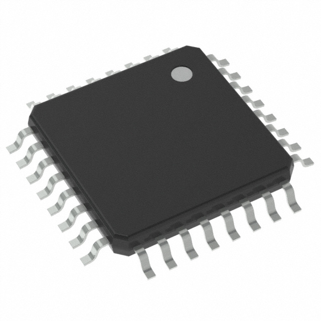


 工商网监
湘ICP备2023018690号
工商网监
湘ICP备2023018690号

