1N5518B thru 1N5546B-1
Available on
commercial
versions
Qualified Levels:
JAN, JANTX and
JANTXV
Low Voltage Avalanche
500 mW Zener Diodes DO-35
Qualified per MIL-PRF-19500/437
DESCRIPTION
The 1N5518 thru 1N5546 series of 0.5 watt axial-leaded glass Zener Voltage Regulators
provides a selection from 3.3 to 33 volts with tolerances ranging from plus/minus 1% to 20%.
The standard tolerance is plus/minus 5% with the B suffix unless ordered otherwise. These
axial-leaded glass DO-35 Zeners are also available with an internal metallurgical bond option.
This type of bonded Zener package construction is also available in JAN, JANTX, and
JANTXV military qualifications. Microsemi also offers numerous other Zener products to meet
higher and lower power applications.
Important: For the latest information, visit our website http://www.microsemi.com.
FEATURES
•
•
•
•
•
JEDEC registered 1N5518 thru 1N5546.
Voltage tolerances of plus/minus 20%, 10%, 5%, 2%, and 1% available. See Note 1 on page 3.
Internal metallurgical bond option available with “-1” suffix.
JAN, JANTX, and JANTXV qualification per MIL-PRF-19500/437 available (requires metallurgical
bond option as well as plus/minus 5% voltage tolerance or tighter with B-1, C-1 or D-1 suffix).
RoHS compliant versions available (commercial grade only).
DO-35 (DO-204AH)
Package
Also available in:
DO-213AA MELF
(surface mount)
1N5518BUR-1 thru
1N5546BUR-1
APPLICATIONS / BENEFITS
•
•
•
•
•
•
•
Regulates voltage over a broad operating current and temperature range.
Guaranteed voltage regulation (∆V Z ) from I ZL to I ZT .
Voltage selection from 3.3 to 33 V.
Flexible axial-lead mounting terminals.
Nonsensitive to ESD per MIL-STD-750 Method 1020.
Minimal capacitance (see Figure 3).
Inherently radiation hard as described in Microsemi “MicroNote 050” which is available at
Microsemi.com.
MAXIMUM RATINGS
Parameters/Test Conditions
Junction and Storage Temperature
(Note 1)
Steady-State Power
Symbol
Value
T J and T STG
PD
-65 to +175
0.5
R ӨJL
R ӨJA
VF
T SP
250
300
1.1
260
Unit
o
C
W
(Also see derating in Figure 2)
(Note 2)
Thermal Resistance Junction-to-Lead
(Note 3)
Thermal Resistance Junction-to-Ambient
Forward Voltage @ 200 mA
Solder Pad Temperature @ 10 s
o
o
C/W
C/W
V
o
C
Notes: 1. At T L < 50 oC 3/8 inch (10 mm) from body or 0.48 W at T A < 25 ºC when mounted on FR4 PC board as
described for thermal resistance above.
2. At 3/8 (10 mm) lead length from body.
3. When mounted on FR4 PC board (1 oz Cu) with 4 mm2 copper pads and track width 1 mm, length 25 mm.
T4-LDS-0037-1, Rev 1 (111456)
©2011 Microsemi Corporation
MSC – Lawrence
6 Lake Street,
Lawrence, MA 01841
1-800-446-1158
(978) 620-2600
Fax: (978) 689-0803
MSC – Ireland
Gort Road Business Park,
Ennis, Co. Clare, Ireland
Tel: +353 (0) 65 6840044
Fax: +353 (0) 65 6822298
Website:
www.microsemi.com
Page 1 of 5
�1N5518B thru 1N5546B-1
MECHANICAL and PACKAGING
•
•
•
•
•
•
•
CASE: Hermetically sealed axial-lead glass DO-35 (DO-204AH) package.
TERMINALS: Leads, tin-lead plated solderable per MIL-STD-750, method 2026. RoHS compliant matte-Tin available for
commercial only.
POLARITY: Cathode indicated by band where diode is to be operated with the banded end positive with respect to the opposite
end for Zener regulation.
MARKING: Part number.
TAPE & REEL option: Standard per EIA-296 (add “TR” suffix to part number). Consult factory for quantities.
WEIGHT: 0.2 grams.
See Package Dimensions on last page.
PART NOMENCLATURE
JAN
1N5518 B -1
(e3)
Reliability Level
JAN = JAN Level
JANTX = JANTX Level
JANTXV = JANTXV Level
Blank = Commercial
RoHS Compliance
e3 = RoHS compliant (available
on commercial grade only)
Blank = non-RoHS compliant
Metallurgical Bond
-1 = Metallurgical bond
blank = Standard bond
JEDEC type number
(see Electrical Characteristic
table)
Zener Voltage Tolerance
A = 10%
B = 5%
C = 2%
D = 1%
Blank = 20%
SYMBOLS & DEFINITIONS
Symbol
IR
I Z , I ZT , I ZK
I ZL
I ZM
VZ
∆V Z
Z ZT or Z ZK
Definition
Reverse Current: The maximum reverse (leakage) current that will flow at the specified voltage and temperature.
Regulator Current: The dc regulator current (I Z ), at a specified test point (I ZT ), near breakdown knee (I ZK ).
Low Regulator (Zener) Current: The lowest rated dc current for the specified power rating.
Maximum Regulator (Zener) Current: The maximum rated dc current for the specified power rating.
Zener Voltage: The zener voltage the device will exhibit at a specified current (I Z ) in its breakdown region.
Voltage Regulation: The change in zener voltage between two specified currents or percentage of I ZM .
Dynamic Impedance: The small signal impedance of the diode when biased to operate in its breakdown region at a
specified rms current modulation (typically 10% of I ZT or I ZK ) and superimposed on I ZT or I ZK respectively.
T4-LDS-0037-1, Rev 1 (111456)
©2011 Microsemi Corporation
Page 2 of 5
�1N5518B thru 1N5546B-1
ELECTRICAL CHARACTERISTICS
(T A = 25oC unless otherwise noted. Based on DC measurements at thermal equilibrium; V F = 1.1 Max @ IF = 200 mA for all types.)
JEDEC
TYPE
NUMBER
(Note 1)
NOMINAL
ZENER
VOLTAGE
TEST
CURRENT
I ZT
MAX. ZENER
IMPEDANCE
B-C-D SUFFIX
V Z @ I ZT
Z ZT @ I ZT
(Note 2)
(Note 3)
MAX. REVERSE LEAKAGE
CURRENT (Note 4)
IR
V R – Volts
B-C-D
SUFFIX
MAXIMUM
DC ZENER
CURRENT
B-C-D SUFFIX
MAX. NOISE
DENSITY
AT I Z = 250µA
REGULATION
FACTOR
LOW V Z
CURRENT
∆V Z
I ZL
(Note 6)
(Note 6)
ND
I ZM
Volts
1N5518
1N5519
1N5520
1N5521
1N5522
1N5523
1N5524
1N5525
1N5526
1N5527
1N5528
1N5529
1N5530
1N5531
1N5532
1N5533
1N5534
1N5535
1N5536
1N5537
1N5538
1N5539
1N5540
1N5541
1N5542
1N5543
1N5544
1N5545
1N5546
3.3
3.6
3.9
4.3
4.7
5.1
5.6
6.2
6.8
7.5
8.2
9.1
10.0
11.0
12.0
13.0
14.0
15.0
16.0
17.0
18.0
19.0
20.0
22.0
24.0
25.0
28.0
30.0
33.0
mA
20
20
20
20
10
5.0
3.0
1.0
1.0
1.0
1.0
1.0
1.0
1.0
1.0
1.0
1.0
1.0
1.0
1.0
1.0
1.0
1.0
1.0
1.0
1.0
1.0
1.0
1.0
Ohms
µA
NON & ASUFFIX
B-C-D
SUFFIX
(Note 5)
mAdc
µV/ √Hz
Volts
mA
26
24
22
18
22
26
30
30
30
35
40
45
60
80
90
90
100
100
100
100
100
100
100
100
100
100
100
100
100
5.0
3.0
1.0
3.0
2.0
2.0
2.0
1.0
1.0
0.5
0.5
0.1
0.05
0.05
0.05
0.01
0.01
0.01
0.01
0.01
0.01
0.01
0.01
0.01
0.01
0.01
0.01
0.01
0.01
0.90
0.90
0.90
1.0
1.5
2.0
3.0
4.5
5.5
6.0
6.5
7.0
8.0
9.0
9.5
10.5
11.5
12.5
13.0
14.0
15.0
16.0
17.0
18.0
20.0
21.0
23.0
24.0
28.0
1.0
1.0
1.0
1.5
2.0
2.5
3.5
5.0
6.2
6.8
7.5
8.2
9.1
9.9
10.8
11.7
12.6
13.5
14.4
15.3
16.2
17.1
18.0
19.8
21.6
22.4
25.2
27.0
29.7
115
105
98
88
81
75
68
61
56
51
46
42
38
35
32
29
27
25
24
22
21
20
19
17
16
15
14
13
12
0.5
0.5
0.5
0.5
0.5
0.5
1.0
1.0
1.0
2.0
4.0
4.0
4.0
5.0
10
15
20
20
20
20
20
20
20
25
30
35
40
45
50
0.90
0.90
0.85
0.75
0.60
0.65
0.30
0.20
0.10
0.05
0.05
0.05
0.10
0.20
0.20
0.20
0.20
0.20
0.20
0.20
0.20
0.20
0.20
0.25
0.30
0.35
0.40
0.45
0.50
2.0
2.0
2.0
2.0
1.0
0.25
0.25
0.01
0.01
0.01
0.01
0.01
0.01
0.01
0.01
0.01
0.01
0.01
0.01
0.01
0.01
0.01
0.01
0.01
0.01
0.01
0.01
0.01
0.01
NOTES:
1. TOLERANCE AND VOLTAGE DESIGNATION –
The JEDEC type numbers shown are +/-20% with guaranteed limits for only V Z , I R , and V F . Units with A suffix are +/-10% with
guaranteed limits for V Z , I R , and V F . Units with guaranteed limits for all six parameters are indicated by a B suffix for +/-5.0% units,
C suffix for +/-2.0% and D suffix for +/-1.0%.
2. ZENER VOLTAGE (V Z ) MEASUREMENT –
Nominal zener voltage is measured with the device junction in thermal equilibrium with ambient temperature of 25 oC.
3. ZENER IMPEDANCE (Z Z ) MEASUREMENT –
The zener impedance is derived from the 60 Hz ac voltage, which results when an ac current having an rms value equal to 10%
of the dc zener current (I ZT ) is superimposed on I ZT .
4. REVERSE LEAKAGE CURRENT (I R ) –
Reverse leakage currents are guaranteed and are measured at V R as shown on the table.
5. MAXIMUM REGULATOR CURRENT (I ZM ) –
The maximum current shown is as shown in MIL-PRF-19500/437.
6. MAXIMUM REGULATION FACTOR (∆V Z ) –
∆V Z is the maximum difference between V Z at I ZT and V Z at I ZL measured with the device junction in thermal equilibrium.
T4-LDS-0037-1, Rev 1 (111456)
©2011 Microsemi Corporation
Page 3 of 5
�1N5518B thru 1N5546B-1
GRAPHS
Rated Maximum DC Operation (mW)
Noise density, (ND) is specified in microvolts rms per
square-root-hertz (µV/ √Hz). Actual measurement is
performed using a 1 kHz to 3 kHz frequency bandpass
filter with a constant Zener test current (IZT) at 25 oC
ambient temperature.
FIGURE 1
Noise Density Measurement Circuit
o
T L – Lead Temperature ( C) 3/8” from body
TYPICAL CAPACITANCE IN PICOFARADS
FIGURE 2 – Temperature-Power Derating Curve
At zero volts
At –2 volts (VR)
ZENER VOLTAGE V Z
FIGURE 3
Capacitance vs. Zener Voltage
(TYPICAL)
T4-LDS-0037-1, Rev 1 (111456)
FIGURE 4
Zener Diode Characteristics and Symbol Identification
©2011 Microsemi Corporation
Page 4 of 5
�1N5518B thru 1N5546B-1
PACKAGE DIMENSIONS
Ltr
BD
BL
LD
LL
LL 1
Inch
Min
.055
.120
.018
1.000
Dimensions
Millimeters
Max
Min
Max
.090
1.40
2.29
.200
3.05
5.08
.022
0.46
0.56
1.500
25.40
38.10
.050
1.27
Notes
3
3
4
NOTES:
1. Dimensions are in inch.
2. Millimeters are given for general information only.
3. Package contour optional within BD and length BL. Heat slugs, if any, shall be included within this cylinder
but shall not be subject to minimum limit of BD. The BL dimension shall include the entire body including
slugs.
4. Within this zone lead, diameter may vary to allow for lead finishes and irregularities other than heat slugs.
5. In accordance with ASME Y14.5M, diameters are equivalent to Φx symbology.
T4-LDS-0037-1, Rev 1 (111456)
©2011 Microsemi Corporation
Page 5 of 5
�
很抱歉,暂时无法提供与“JAN1N5541B-1/TR”相匹配的价格&库存,您可以联系我们找货
免费人工找货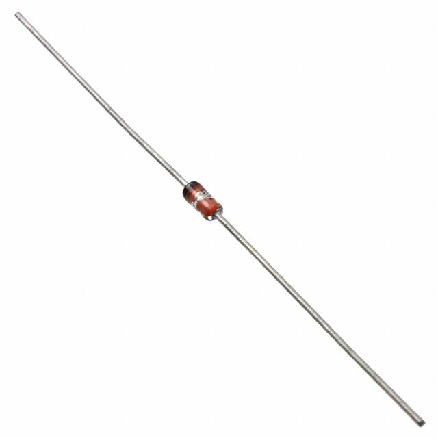


 工商网监
湘ICP备2023018690号
工商网监
湘ICP备2023018690号
