LAN8820/LAN8820i
RGMII 10/100/1000 Ethernet Transceiver
with HP Auto-MDIX Support
Highlights
Key Benefits
• Single-Chip Ethernet Physical Layer Transceiver
(PHY)
• Compliant with IEEE 802.3ab (1000BASE-T),
IEEE 802.3u (Fast Ethernet), and ISO 802-3/IEEE
802.3 (10BASE-T)
• HP Auto-MDIX support in accordance with IEEE
802.3ab specification at 10/100/1000 Mbps operation
• Miniature 56-pin QFN lead-free RoHS compliant
package with RGMII (8 x 8 x 0.85 mm height)
• Implements Reduced Power Operating Modes
• High-Performance 10/100/1000 Ethernet Transceiver
- Compliant with IEEE 802.3ab (1000BASE-T)
- Compliant with IEEE 802.3/802.3u (Fast
Ethernet)
- Compliant with ISO 802-3/IEEE 802.3
(10BASE-T)
- 10BASE-T, 100BASE-TX and 1000BASE-T
support
- Loop-back modes
- Auto-negotiation (NEXT page support)
- Automatic polarity detection and correction
- Link status change wake-up detection
- Vendor specific register functions
- Supports reduced pin count RGMII interface
Target Applications
•
•
•
•
•
•
•
•
•
•
•
•
•
•
•
Set-Top Boxes
Networked Printers and Servers
Test Instrumentation
LAN on Motherboard
Embedded Telecom Applications
Video Record/Playback Systems
Cable Modems/Routers
DSL Modems/Routers
Digital Video Recorders
IP and Video Phones
Wireless Access Points
Digital Televisions
Digital Media Adapters/Servers
Gaming Consoles
POE Applications
- Controlled impedance outputs
- Supports RGMII ID mode
- Three status LED outputs
- Compliant with IEEE 802.3-2005 standards
- RGMII pins tolerant to 3.6V
•
•
•
•
2009-2018 Microchip Technology Inc.
- Integrated DSP implements adaptive equalizer, echo cancelers, and crosstalk cancelers
- Efficient digital baseline wander correction
Power and I/Os
- Various low power modes
- 2.5V I/O supply
Miscellaneous Features
- IEEE 1149.1 (JTAG) boundary scan
- Multiple clock options - 25MHz crystal or
25MHz single-ended clock
Packaging
- 56-pin QFN (8x8 mm) RoHS compliant package with RGMII
Environmental
- Commercial temperature range
(0°C to +70°C)
- Industrial temperature range (-40°C to
+85°C)
DS00001871D-page 1
�LAN8820/LAN8820i
TO OUR VALUED CUSTOMERS
It is our intention to provide our valued customers with the best documentation possible to ensure successful use of your Microchip
products. To this end, we will continue to improve our publications to better suit your needs. Our publications will be refined and
enhanced as new volumes and updates are introduced.
If you have any questions or comments regarding this publication, please contact the Marketing Communications Department via
E-mail at docerrors@microchip.com. We welcome your feedback.
Most Current Data Sheet
To obtain the most up-to-date version of this data sheet, please register at our Worldwide Web site at:
http://www.microchip.com
You can determine the version of a data sheet by examining its literature number found on the bottom outside corner of any page.
The last character of the literature number is the version number, (e.g., DS30000000A is version A of document DS30000000).
Errata
An errata sheet, describing minor operational differences from the data sheet and recommended workarounds, may exist for current devices. As device/documentation issues become known to us, we will publish an errata sheet. The errata will specify the
revision of silicon and revision of document to which it applies.
To determine if an errata sheet exists for a particular device, please check with one of the following:
• Microchip’s Worldwide Web site; http://www.microchip.com
• Your local Microchip sales office (see last page)
When contacting a sales office, please specify which device, revision of silicon and data sheet (include -literature number) you are
using.
Customer Notification System
Register on our web site at www.microchip.com to receive the most current information on all of our products.
DS00001871D-page 2
2009-2018 Microchip Technology Inc.
�LAN8820/LAN8820i
Table of Contents
1.0 Introduction ..................................................................................................................................................................................... 4
2.0 Pin Description and Configuration .................................................................................................................................................. 5
3.0 Functional Description .................................................................................................................................................................. 13
4.0 Register Descriptions .................................................................................................................................................................... 34
5.0 Operational Characteristics ........................................................................................................................................................... 60
6.0 Package Outline ............................................................................................................................................................................ 76
Appendix A: Data Sheet Revision History ........................................................................................................................................... 78
The Microchip Web Site ...................................................................................................................................................................... 81
Customer Change Notification Service ............................................................................................................................................... 81
Customer Support ............................................................................................................................................................................... 81
Product Identification System ............................................................................................................................................................. 82
2009-2018 Microchip Technology Inc.
DS00001871D-page 3
�LAN8820/LAN8820i
1.0
INTRODUCTION
The LAN8820/LAN8820i is a low-power 10BASE-T/100BASE-TX/1000BASE-T Gigabit Ethernet physical layer (PHY)
transceiver that is fully compliant with the IEEE 802.3 and 802.3ab standards.
The LAN8820/LAN8820i can be configured to communicate with an Ethernet MAC via the standard RGMII interface. It
contains a full-duplex transceiver for 1000 Mbps operation on four pairs of category 5 or better balanced twisted pair
cable. Per IEEE 802.3-2005 standards, all digital interface pins are tolerant to 3.6V.
The LAN8820/LAN8820i is configurable via hardware and software, supporting both IEEE 802.3-2005 compliant and
vendor-specific register functions via SMI. The LAN8820/LAN8820i implements Auto-Negotiation to automatically
determine the best possible speed and duplex mode of operation. HP Auto-MDIX support allows the use of direct connect or crossover cables.
An internal block diagram of the LAN8820/LAN8820i is shown in Figure 1-1. A typical system-level diagram is shown in
Figure 1-2.
FIGURE 1-1:
INTERNAL BLOCK DIAGRAM
3
3
PLL
LEDs
2
Digital TX
2
Scrambler
Trellis
4DPAM-5 Encoders
1
0
0
Spectral
Shaper
LEDs
3
3
2
2
1
3
2
1
1
0
1
0
Analog
TX
0
3
2
RGMII
JTAG
Physical
Coding
Sublayer
TAP
Controller
1
10/100/1000
Ethernet
0
Active
Hybrid
3
Digital RX
2
Descrambler
Viterbi Decoder
4DPAM-5 Decoders
1
3
3
2
2
1
0
0
DSP
3
3
2
1
0
2
1
1
0
0
Analog
RX
LAN8820/LAN8820i
FIGURE 1-2:
SYSTEM LEVEL BLOCK DIAGRAM
Crystal
10/100/1000
Ethernet MAC
RGMII
LAN8820/
LAN8820i
JTAG
DS00001871D-page 4
MDI
Ethernet
Magnetics
Ethernet
LED
Status
2009-2018 Microchip Technology Inc.
�LAN8820/LAN8820i
2.0
PIN DESCRIPTION AND CONFIGURATION
FIGURE 2-1:
56-QFN PIN ASSIGNMENTS (TOP VIEW)
TR0N
43
28
TXCTRL
TR0P
44
27
TXD0
VDD12A
45
26
TXD1
TR1N
46
LAN8820/LAN8820i
56 PIN QFN
25
TXD2
TR1P
47
(TOP VIEW)
24
VDD25IO
VDD12A
48
23
VDD12CORE
VDD12BIAS
49
22
TXD3
VDD12PLL
50
21
NC
TR2N
51
20
VDD12CORE
TR2P
52
19
VDD25IO
VDD12A
53
18
RXC
TR3N
54
17
IRQ
TR3P
55
16
nRESET
VDD12A
56
15
HPD
VSS
NOTE: Exposed pad (VSS) on bottom of package must be connected to ground
2009-2018 Microchip Technology Inc.
DS00001871D-page 5
�LAN8820/LAN8820i
TABLE 2-1:
Num
Pins
1
1
1
1
RGMII INTERFACE PINS
Buffer
Type
Name
Symbols
Transmit Data 0
TXD0
IS
(PD)
The MAC transmits data to the PHY using this
signal.
Transmit Data 1
TXD1
IS
(PD)
The MAC transmits data to the PHY using this
signal.
Transmit Data 2
TXD2
IS
(PD)
The MAC transmits data to the PHY using this
signal.
Transmit Data 3
TXD3
IS
(PD)
The MAC transmits data to the PHY using this
signal.
Transmit
Control
TXCTRL
IS
(PD)
Indicates both the transmit data enable (TXEN) and
transmit error (TXER) functions per the RGMII
specification.
Transmit Clock
TXC
IS
(PD)
Used to latch data from the MAC into the PHY.
1
1
Description
1000BASE-T: 125MHz
100BASE-TX: 25MHz
10BASE-T: 2.5MHz
1
Receive Data 0
RXD0
O6
The PHY transfers data to the MAC using this
signal.
1
Receive Data 1
RXD1
O6
The PHY transfers data to the MAC using this
signal.
1
Receive Data 2
RXD2
O6
The PHY transfers data to the MAC using this
signal.
1
Receive Data 3
RXD3
O6
The PHY transfers data to the MAC using this
signal.
Receive Control
RXCTRL
O6
Indicates both the receive data valid (RXDV) and
receive error (RXER) functions per the RGMII
specification.
Receive Clock
RXC
O6
Used to transfer data to the MAC.
1
1
Note 2-1
1000BASE-T: 125 MHz
100BASE-TX: 25 MHz
10BASE-T: 2.5 MHz
Configuration strap values are latched on hardware reset. Configuration straps are identified by an
underlined symbol name. Signals that function as configuration straps must be augmented with an
external resistor when connected to a load. Refer to Section 3.8, "Configuration," on page 23 for
additional information.
DS00001871D-page 6
2009-2018 Microchip Technology Inc.
�LAN8820/LAN8820i
TABLE 2-2:
Num
Pins
1
1
SERIAL MANAGEMENT INTERFACE (SMI) PINS
Buffer
Type
Name
Symbols
SMI Clock
MDC
IS
(PD)
Serial Management Interface clock.
SMI Data Input/
Output
MDIO
IS/O8
(PU)
Serial Management Interface data input/output.
TABLE 2-3:
Description
LED & CONFIGURATION PINS
Num
Pins
Name
Symbols
Buffer
Type
1
10BASE-T Link
LED Indicator
10_LED
O8
10BASE-T LED link indication. Refer to Section
3.9.1, "LEDs," on page 27 for additional
information.
100BASE-TX
Link LED
Indicator
100_LED
O8
100BASE-TX LED link indication. Refer to Section
3.9.1, "LEDs," on page 27 for additional
information.
Hardware
Power Down
(HPD) Mode
Configuration
Strap
HPD_MODE
IS
(PD)
This configuration strap is used to select the
Hardware Power Down (HPD) mode. When pulledup, the PLL is not disabled when HPD is asserted.
When pulled-down, the PLL is disabled when HPD
is asserted.
1
Description
Refer to Section 3.7.3, "Hardware Power-Down,"
on page 23 for additional information.
See Note 2-2 for more information on configuration
straps.
1
1000BASE-T
Link LED
Indicator
1000_LED
O8
1000BASE-T LED link indication. Refer to Section
3.9.1, "LEDs," on page 27 for additional
information.
RGMII ID Mode
Enable
Configuration
Strap
RGMII_ID_MODE
IS
(PD)
This configuration strap is used to configure the
RGMII PHY TXC/RXC delay enable bit defaults.
When pulled-up, the RGMII PHY TXC/RXC delays
are enabled by default. When pulled-down, the
RGMII PHY TXC/RXC delays are disabled be
default.
Refer to Section 3.3, "RGMII Interface," on page 18
for more information. See Note 2-2 for more
information on configuration straps.
Configuration
Input 0
CONFIG0
IS
(PD)
This pin sets the PHYADD[1:0] bits of the 10/100
Special Modes Register on reset or power-up. It
must be connected to VSS, 100_LED, 1000_LED,
or VDD25IO. Refer to Section 3.8.1.2,
"CONFIG[3:0] Configuration Pins," on page 24 for
additional information.
Configuration
Input 1
CONFIG1
IS
(PD)
This pin sets the PAUSE bit of the Auto Negotiation
Advertisement Register and PHYADD [2] bit of the
10/100 Special Modes Register on reset or powerup. It must be connected to VSS, 100_LED,
1000_LED, or VDD25IO. Refer to Section 3.8.1.2,
"CONFIG[3:0] Configuration Pins," on page 24 for
additional information.
1
1
2009-2018 Microchip Technology Inc.
DS00001871D-page 7
�LAN8820/LAN8820i
TABLE 2-3:
Num
Pins
LED & CONFIGURATION PINS (CONTINUED)
Buffer
Type
Name
Symbols
Configuration
Input 2
CONFIG2
IS
(PD)
This pin sets the MOD[1:0] bits of the Extended
Mode Control/Status Register on reset or powerup. It must be connected to VSS, 100_LED,
1000_LED, or VDD25IO. Refer to Section 3.8.1.2,
"CONFIG[3:0] Configuration Pins," on page 24 for
additional information.
Configuration
Input 3
CONFIG3
IS
(PD)
This pin sets the MOD[3] bit of the Extended Mode
Control/Status Register on reset or power-up. It
must be connected to 1000_LED. Refer to Section
3.8.1.2, "CONFIG[3:0] Configuration Pins," on
page 24 for additional information.
1
1
Note 2-2
TABLE 2-4:
Description
Configuration strap values are latched on hardware reset. Configuration straps are identified by an
underlined symbol name. Signals that function as configuration straps must be augmented with an
external resistor when connected to a load. Refer to Section 3.8, "Configuration," on page 23 for
additional information.
ETHERNET PINS
Num Pins
Name
Symbol
Buffer
Type
1
Ethernet TX/
RX Positive
Channel 0
TR0P
AIO
Transmit/Receive Positive Channel 0.
1
Ethernet TX/
RX Negative
Channel 0
TR0N
AIO
Transmit/Receive Negative Channel 0.
1
Ethernet TX/
RX Positive
Channel 1
TR1P
AIO
Transmit/Receive Positive Channel 1.
1
Ethernet TX/
RX Negative
Channel 1
TR1N
AIO
Transmit/Receive Negative Channel 1.
1
Ethernet TX/
RX Positive
Channel 2
TR2P
AIO
Transmit/Receive Positive Channel 2.
1
Ethernet TX/
RX Negative
Channel 2
TR2N
AIO
Transmit/Receive Negative Channel 2.
1
Ethernet TX/
RX Positive
Channel 3
TR3P
AIO
Transmit/Receive Positive Channel 3.
1
Ethernet TX/
RX Negative
Channel 3
TR3N
AIO
Transmit/Receive Negative Channel 3.
1
External PHY
Bias Resistor
ETHRBIAS
AI
DS00001871D-page 8
Description
Used for the internal bias circuits. Connect to an
external 8.06K 1.0% resistor to ground.
2009-2018 Microchip Technology Inc.
�LAN8820/LAN8820i
TABLE 2-5:
JTAG PINS
Num Pins
Name
Symbol
Buffer
Type
1
JTAG Test
Data Out
TDO
O8
1
JTAG Test
Data Input
TDI
IS
(PU)
JTAG (IEEE 1149.1) data input.
1
JTAG Test
Clock
TCK
IS
(PD)
JTAG (IEEE 1149.1) test clock.
1
JTAG Test
Mode Select
TMS
IS
(PU)
JTAG (IEEE 1149.1) test mode select.
TABLE 2-6:
Num Pins
Description
JTAG (IEEE 1149.1) data output.
Note:
Note:
Note:
When not used, tie this pin to VDD25IO.
When not used, tie this pin to VSS.
When not used, tie this pin to VDD25IO.
MISCELLANEOUS PINS
Name
Symbol
Buffer
Type
Crystal Input
XI
ICLK
Description
External 25 MHz crystal input.
Note:
1
This pin can also be driven by a 25 MHz
single-ended clock oscillator. When this
method is used, XO should be left
unconnected. Refer to Section 5.6,
"Clock Circuit," on page 75 for additional
information.
Crystal
Output
XO
OCLK
System Reset
nRESET
IS
(PU)
Interrupt
Request
IRQ
O6
Hardware
Power Down
HPD
1
IS
(PD)
When asserted, this pin places the device into
Hardware Power Down (HPD) mode. Refer to
Section 3.7.3, "Hardware Power-Down," on
page 23 for additional information.
1
No Connect
NC
-
This pin must be left floating for normal device
operation.
1
1
1
2009-2018 Microchip Technology Inc.
External 25 MHz crystal output.
This active-low pin allows external hardware to
reset the device.
Programmable interrupt request.
Note:
When used, this pin requires an
external 4.7K pull-up resistor.
DS00001871D-page 9
�LAN8820/LAN8820i
TABLE 2-7:
POWER PINS
Num Pins
Name
Symbol
Buffer
Type
+2.5V
I/O Power
Supply Input
VDD25IO
P
4
+2.5V I/O power.
Refer to Section 3.10, "Application Diagrams," on
page 31 and the LAN8820/LAN8820i reference
schematics for connection information.
6
Digital Core
+1.2V Power
Supply Input
VDD12CORE
P
Refer to Section 3.10, "Application Diagrams," on
page 31 and the LAN8820/LAN8820i reference
schematics for connection information.
VDD12A
P
4
Ethernet
+1.2V Port
Power Supply
Input For
Channels 0-3
Refer to Section 3.10, "Application Diagrams," on
page 31 and the LAN8820/LAN8820i reference
schematics for connection information.
Ethernet
+1.2V Bias
Power Supply
Input
VDD12BIAS
P
Refer to Section 3.10, "Application Diagrams," on
page 31 and the LAN8820/LAN8820i reference
schematics for connection information.
1
Ethernet PLL
+1.2V Power
Supply Input
VDD12PLL
P
Refer to Section 3.10, "Application Diagrams," on
page 31 and the LAN8820/LAN8820i reference
schematics for connection information.
Note 2-3
Ground
VSS
P
Common Ground
1
Note 2-3
Description
Exposed pad on package bottom (Figure 2-1).
DS00001871D-page 10
2009-2018 Microchip Technology Inc.
�LAN8820/LAN8820i
TABLE 2-8:
56-QFN PIN ASSIGNMENTS
Pin
Num
Pin Name
Pin
Num
Pin Name
Pin
Num
Pin Name
Pin
Num
Pin Name
1
TDI
15
HPD
29
TXC
43
TR0N
2
TCK
16
nRESET
30
VDD12CORE
44
TR0P
3
TMS
17
IRQ
31
1000_LED/
45
VDD12A
4
TDO
18
RXC
32
100_LED/
HPD_MODE
46
TR1N
5
XI
19
VDD25IO
33
10_LED
47
TR1P
6
XO
20
VDD12CORE
34
CONFIG3
48
VDD12A
7
VDD25IO
21
NC
35
CONFIG2
49
VDD12BIAS
8
VDD12CORE
22
TXD3
36
VDD12CORE
50
VDD12PLL
9
RXD0
23
VDD12CORE
37
VDD25IO
51
TR2N
10
RXD1
24
VDD25IO
38
CONFIG1
52
TR2P
11
RXD2
25
TXD2
39
CONFIG0
53
VDD12A
12
RXD3
26
TXD1
40
MDC
54
TR3N
13
VDD12CORE
27
TXD0
41
MDIO
55
TR3P
14
RXCTRL
28
TXCTRL
42
ETHRBIAS
56
VDD12A
RGMII_ID_MODE
EXPOSED PAD
MUST BE CONNECTED TO VSS
2009-2018 Microchip Technology Inc.
DS00001871D-page 11
�LAN8820/LAN8820i
2.1
Buffer Types
TABLE 2-9:
BUFFER TYPES
Buffer Type
Description
IS
Schmitt-triggered input.
O6
Output with 6 mA sink and 6 mA source.
O8
Output with 8 mA sink and 8 mA source.
PU
50uA (typical) internal pull-up. Unless otherwise noted in the pin description, internal pullups are always enabled.
Note:
PD
50uA (typical) internal pull-down. Unless otherwise noted in the pin description, internal
pull-downs are always enabled.
Note:
AI
Internal pull-up resistors prevent unconnected inputs from floating. Do not rely on
internal resistors to drive signals external to the device. When connected to a load
that must be pulled high, an external resistor must be added.
Internal pull-down resistors prevent unconnected inputs from floating. Do not rely
on internal resistors to drive signals external to the device. When connected to a
load that must be pulled low, an external resistor must be added.
Analog input.
AIO
Analog bi-directional.
ICLK
Crystal oscillator input pin.
OCLK
Crystal oscillator output pin.
P
Power pin.
Note 1: The digital signals are not 5V tolerant. Refer to Section 5.1, "Absolute Maximum Ratings*," on page 60 for
additional buffer information.
DS00001871D-page 12
2009-2018 Microchip Technology Inc.
�LAN8820/LAN8820i
3.0
FUNCTIONAL DESCRIPTION
This chapter provides functional descriptions of the various device features. These features have been categorized into
the following sections:
•
•
•
•
•
•
•
•
•
•
Auto-negotiation
HP Auto-MDIX
RGMII Interface
Serial Management Interface (SMI)
Interrupt Management
Resets
Power-Down modes
Configuration
Miscellaneous Functions
Application Diagrams
3.1
Auto-negotiation
The purpose of the auto-negotiation function is to automatically configure the PHY to the optimum link parameters based
on the capabilities of its link partner. Auto-negotiation is a mechanism for exchanging configuration information between
two link-partners and automatically selecting the highest performance mode of operation supported by both sides. Autonegotiation is fully defined in clause 28 and clause 40 of the IEEE 802.3 specification.
Once auto-negotiation has completed, information about the resolved link can be passed back to the controller via the
integrated Serial Management Interface (SMI). The results of the negotiation process are reflected in the Speed Indication field of the PHY Special Control / Status Register as well as the Auto Negotiation Link Partner Ability Register.
The advertised capabilities of the PHY are stored in Auto Negotiation Advertisement Register. The defaults advertised
by the device are determined as described in Section 3.8.1.2.2, "Configuring the Mode of Operation (CONFIG[3:2])," on
page 26.
The auto-negotiation protocol is a purely physical layer activity and proceeds independently of the MAC controller. When
enabled, auto-negotiation is started by the occurrence of one of the following events:
•
•
•
•
•
Hardware reset
Software reset
Power-down reset
Link status down
Setting the Restart Auto-Negotiate bit of the Basic Control Register
On detection of one of these events, the device begins auto-negotiation by transmitting bursts of Fast Link Pulses (FLP).
The data transmitted by an FLP burst is known as a “Link Code Word.” This exchange of information allows link partners
to determine the Highest Common Ability (HCD).
Once a capability match has been determined, the link code words are repeated with the acknowledge bit set. Any difference in the main content of the link code words at this time will cause auto-negotiation to re-start. Auto-negotiation
will also re-start if all of the required FLP bursts are not received.
Writing the 100BASE-TX Full Duplex, 100BASE-TX, 10BASE-T Full Duplex, and 10BASE-T bits of the Auto Negotiation
Advertisement Register allows software control of the advertised capabilities. However, writing the Auto Negotiation
Advertisement Register does not automatically re-start auto-negotiation. The Restart Auto-Negotiate bit of the Basic
Control Register must be set before the new abilities will be advertised. Auto-negotiation can also be disabled via software by clearing the Auto-Negotiation Enable bit of the Basic Control Register.
Auto-Negotiation also resolves the Master/Slave clocking relationship between two PHYs for a 1000BASE-T link. Refer
to Section 3.1.4, "Master/Slave," on page 14 for additional information.
3.1.1
RESTARTING AUTO-NEGOTIATION
Auto-negotiation can be restarted at any time by using the Restart Auto-Negotiate bit of the Basic Control Register.
Auto-negotiation will also re-start if the link is broken at any time. A broken link is caused by signal loss. This may occur
because of a cable break, or because of an interruption in the signal transmitted by the Link Partner. Auto-negotiation
resumes in an attempt to determine the new link configuration.
2009-2018 Microchip Technology Inc.
DS00001871D-page 13
�LAN8820/LAN8820i
If the management entity restarts Auto-negotiation by writing to the Restart Auto-Negotiate bit, the device will respond
by stopping all transmission/receiving operations. Auto-negotiation will restart after approximately 1200 mS. The Link
Partner will have also dropped the link and will resume auto-negotiation.
3.1.2
DISABLING AUTO-NEGOTIATION
Auto-negotiation can be disabled via software by clearing the Auto-Negotiation Enable bit of the Basic Control Register.
The device will then force its speed of operation to reflect the information in the Speed Select[1], Speed Select[0], and
Duplex Mode bits of the Basic Control Register. These bits are ignored when auto-negotiation is enabled.
3.1.3
PARALLEL DETECTION
If the LAN8820/LAN8820i is connected to a device lacking the ability to auto-negotiate (for example, no FLPs are
detected), it is able to determine the speed of the link based on either 100M MLT-3 symbols or 10M Normal Link Pulses.
In this case, the link is presumed to be half-duplex per the IEEE standard. This ability is known as “Parallel Detection”.
This feature ensures inter operability with legacy link partners.
The Ethernet MAC has access to information regarding parallel detect via the Auto Negotiation Expansion Register. If
a link is formed via parallel detection, the Link Partner Auto-Negotiation Able bit of the Auto Negotiation Expansion Register is cleared to indicate that the Link Partner is not capable of auto-negotiation. If a fault occurs during parallel detection, the Parallel Detection Fault bit of this register is set.
The Auto Negotiation Link Partner Ability Register is updated with information from the link partner which is coded in the
received FLPs. If the Link Partner is not auto-negotiation capable, then the Auto Negotiation Link Partner Ability Register
is updated after completion of parallel detection to reflect the speed capability of the Link Partner.
Parallel detect cannot be used to establish Gigabit Ethernet links because echo cancellation and signal recovery on a
Gigabit Ethernet link requires resolution of the Master/Slave clock relationship, which requires the exchange of FLPs.
3.1.4
MASTER/SLAVE
In 1000BASE-T, one of the two link partner devices must be configured as Master and the other as Slave. The Master
device transmits data using the local clock, while the Slave device uses the clock recovered from incoming data.
The Master and Slave assignments are set using the configuration pins as described in Section 3.8.1.2.2, "Configuring
the Mode of Operation (CONFIG[3:2])," on page 26 or by using the Master/Slave Manual Config Enable and Master/
Slave Manual Config Value bits of the Master/Slave Control Register. If both the link partner and the local device are
manually given the same Master/Slave assignment, an error will be indicated in the Master/Slave Configuration Fault
bit of the Master/Slave Status Register.
Depending on the link partner configuration, the manual Master/Slave mode can be resolved to sixteen possible outcomes, as shown in Table 3-1.
TABLE 3-1:
MASTER/SLAVE RESOLUTION FOR 1000BASE-T
LAN8820/LAN8820i
Advertisement
Link Partner
Advertisement
LAN8820/LAN8820i Result
Link Partner Result
Single-Port
Single-Port
M/S resolved by random seed
M/S resolved by random seed
Single-Port
Multi-Port
Slave
Master
Single-Port
Manual Master
Slave
Master
Single-Port
Manual Slave
Master
Slave
Multi-Port
Single-Port
Master
Slave
Multi-Port
Multi-Port
M/S resolved by random seed
M/S resolved by random seed
Multi-Port
Manual Master
Slave
Master
Multi-Port
Manual Slave
Master
Slave
Manual Master
Single-Port
Master
Slave
DS00001871D-page 14
2009-2018 Microchip Technology Inc.
�LAN8820/LAN8820i
TABLE 3-1:
MASTER/SLAVE RESOLUTION FOR 1000BASE-T (CONTINUED)
LAN8820/LAN8820i
Advertisement
Link Partner
Advertisement
LAN8820/LAN8820i Result
Link Partner Result
Manual Master
Multi-Port
Master
Slave
Manual Master
Manual Master
No Link
No Link
Manual Master
Manual Slave
Master
Slave
Manual Slave
Single-Port
Slave
Master
Manual Slave
Multi-Port
Slave
Master
Manual Slave
Manual Master
Slave
Master
Manual Slave
Manual Slave
No Link
No Link
3.1.5
MANUAL OPERATION
The device supports a manual (forced) operation for test purposes. In manual operation, the user sets the link speed
(10Mbps or 100Mbps) and the duplex state (full or half).
Auto-negotiation must be disabled in order to manually configure the speed and the duplex. This may be accomplished
using the configuration pins, as described in Section 3.8.1.2.2, "Configuring the Mode of Operation (CONFIG[3:2])," on
page 26, or by using the Basic Control Register as described in Section 3.1.2, "Disabling Auto-negotiation," on page 14.
For 10BASE-T and 100BASE-TX, the link state of the device is determined by the Speed Select[1], Speed Select[0],
and Duplex Mode bits of the Basic Control Register. Manual operation at a link speed of 1000Mbps is not supported.
3.1.6
HALF VS. FULL-DUPLEX
Half-duplex operation relies on the CSMA/CD (Carrier Sense Multiple Access / Collision Detect) protocol to handle network traffic and collisions. In this mode, the internal carrier sense signal, CRS, responds to both transmit and receive
activity. If data is received while the PHY is transmitting, a collision results.
In full-duplex mode, the PHY is able to transmit and receive data simultaneously and collision detection is disabled. In
this mode, the internal CRS responds only to receive activity. In 10BASE-T and 100BASE-T mode, CRS is redefined to
respond only to received activity. In 1000BASE-T, CRS is disabled.
Table 3-2 describes the behavior of the internal CRS bit under all receive/transmit conditions.
TABLE 3-2:
CRS BEHAVIOR
Mode
Speed
Duplex
Activity
CRS Behavior
(Note 3-1)
Manual
10 Mbps
Half-Duplex
Transmitting
Active
Manual
10 Mbps
Half-Duplex
Receiving
Active
Manual
10 Mbps
Full-Duplex
Transmitting
Low
Manual
10 Mbps
Full-Duplex
Receiving
Active
Manual
100 Mbps
Half-Duplex
Transmitting
Active
Manual
100 Mbps
Half-Duplex
Receiving
Active
Manual
100 Mbps
Full-Duplex
Transmitting
Low
Manual
100 Mbps
Full-Duplex
Receiving
Active
Auto-Negotiation
10 Mbps
Half-Duplex
Transmitting
Active
2009-2018 Microchip Technology Inc.
DS00001871D-page 15
�LAN8820/LAN8820i
TABLE 3-2:
CRS BEHAVIOR (CONTINUED)
Mode
Speed
Duplex
Activity
CRS Behavior
(Note 3-1)
Auto-Negotiation
10 Mbps
Half-Duplex
Receiving
Active
Auto-Negotiation
10 Mbps
Full-Duplex
Transmitting
Low
Auto-Negotiation
10 Mbps
Full-Duplex
Receiving
Active
Auto-Negotiation
100 Mbps
Half-Duplex
Transmitting
Active
Auto-Negotiation
100 Mbps
Half-Duplex
Receiving
Active
Auto-Negotiation
100 Mbps
Full-Duplex
Transmitting
Low
Auto-Negotiation
100 Mbps
Full-Duplex
Receiving
Active
Note 3-1
3.2
The internal CRS signal operates in two modes: Active and Low. When in Active mode, the internal
CRS will transition high and low upon line activity, where a high value indicates a carrier has been
detected. In Low mode, the internal CRS stays low and does not indicate carrier detection.
HP Auto-MDIX
HP Auto-MDIX facilitates the use of CAT-5 (100BASE-T) media UTP interconnect cable without consideration of interface wiring scheme. If a user plugs in either a direct connect LAN cable, or a crossover patch cable, as shown in
Figure 3-1, the Auto-MDIX PHY is capable of configuring the twisted pair pins for correct transceiver operation.
The internal logic of the device detects the TX and RX pins of the connecting device. It can automatically re-assign channel 0 and 1 if required to establish a link. In 1000BASE-T mode, it can re-assign channel 2 and 3. Crossover resolution
precedes the actual auto-negotiation process that involves exchange of FLPs to advertise capabilities. Automatic MDI/
MDIX is described in IEEE 802.3ab Clause 40, section 40.8.2. Since the RX and TX line pairs are interchangeable, special PCB design considerations are needed to accommodate the symmetrical magnetics and termination of an AutoMDIX design.
Auto-MDIX is enabled by default, and can be disabled by the Auto MDIX Disable bit in the 10/100 Mode Control/Status
Register. When Auto-MDIX is disabled, the TX and RX pins can be configured manually by the MDI/MDI-X 0:1 and MDI/
MDI-X 2:3 bits in the Extended Mode Control/Status Register.
The device includes an advanced crossover resolution capability called Semi Crossover. This is an extension to HP
Auto-MDIX that corrects for a cable with only two pairs crossed. If Semi Crossover is enabled, after the device has
attempted to establish a link with all four signal pairs normal or crossed, it will attempt to establish a link with pairs 2/3
switched and 0/1 straight, and then with pairs 0/1 switched and pairs 2/3 straight. The Semi Crossover is enabled by
default, and can be disabled by the Semi Crossover Enable bit in the 10/100 Mode Control/Status Register.
After resolution of crossed pairs is complete, using either HP Auto-MDIX or the Semi Crossover function, the MDI/MDIX status is reported through the XOVER Resolution 0:1 and XOVER Resolution 2:3 bits of the User Status 2 Register.
DS00001871D-page 16
2009-2018 Microchip Technology Inc.
�LAN8820/LAN8820i
FIGURE 3-1:
CABLE CONNECTION TYPES: STRAIGHT-THROUGH, CROSSOVER, SEMI
CROSSOVER
RJ-45 8-pin Straight-Through
RJ-45 8-pin Crossover
TR0P
1
1
TR0P
TR0P
1
1
TR0P
TR0N
2
2
TR0N
TR0N
2
2
TR0N
TR1P
3
3
TR1P
TR1P
3
3
TR1P
TR2P
4
4
TR2P
TR2P
4
4
TR2P
TR2N
5
5
TR2N
TR2N
5
5
TR2N
TR1N
6
6
TR1N
TR1N
6
6
TR1N
TR3P
7
7
TR3P
TR3P
7
7
TR3P
TR3N
8
8
TR3N
TR3N
8
8
TR3N
Direct Connect Cable
Crossover Cable
RJ-45 8-pin Semi Crossover
RJ-45 8-pin Semi Crossover
TR0P
1
1
TR0P
TR0P
1
1
TR0P
TR0N
2
2
TR0N
TR0N
2
2
TR0N
TR1P
3
3
TR1P
TR1P
3
3
TR1P
TR2P
4
4
TR2P
TR2P
4
4
TR2P
TR2N
5
5
TR2N
TR2N
5
5
TR2N
TR1N
6
6
TR1N
TR1N
6
6
TR1N
TR3P
7
7
TR3P
TR3P
7
7
TR3P
TR3N
8
8
TR3N
TR3N
8
8
TR3N
0/1 Straight, 2/3 Crossed
3.2.1
0/1 Crossed, 2/3 Straight
REQUIRED ETHERNET MAGNETICS
The magnetics selected for use with the device should be an Auto-MDIX style magnetic available from several vendors.
Refer to Application Note 8.13 “Suggested Magnetics” for the latest qualified and suggested magnetics. Vendors and
part numbers are provided in this application note.
2009-2018 Microchip Technology Inc.
DS00001871D-page 17
�LAN8820/LAN8820i
3.3
RGMII Interface
The device communicates with an external MAC using the Reduced Gigabit Media Independent Interface (RGMII). The
RGMII is compliant with the RGMII standard, and provides support for 1000BASE-T, 100BASE-TX, or 10BASE-T operation.
The RGMII consists of the RXC, RXD[3:0], RXCTRL, TXC, TXD[3:0] and TXCTRL signals. All transmission related signals, TXC, TXD[3:0] and TXCTRL, are generated by the MAC. The TXC transmit clock is used to synchronize the
TXD[3:0] data and TXCTRL control signals. All reception related signals, RXC, RXD[3:0] and RXCTRL, are generated
by the device. The RXC receive clock is used to synchronic the RXD[3:0] data and RXCTRL control signals.
The RGMII interface supports both Version 1.3 and Version 2.0 of the RGMII specification. Version 1.3 of the RGMII
Specification requires a 1.5 to 2ns clock delay via a PCB trace delay. Version 2.0 of the RGMII Specification introduces
the option of an on-chip Internal Delay (ID). These distinct RGMII modes of operation are referred to as “Non-ID Mode”
and “ID Mode”, respectively, throughout the document. Refer to the RGMII specification for additional details.
In addition to the standard Non-ID and ID modes of operation, the device supports a hybrid mode of operation, for a
total of 3 RGMII modes. These modes are summarized below:
Non-ID Mode - Per the RGMII specification, no internal delay is generated at the MAC or the device(PHY). External
PCB trace delays are required to meet RGMII timing requirements.
ID Mode - Per the RGMII specification, an internal delay is generated on TXC at the MAC, and an ID is generated on
RXC at the device(PHY). No PCB trace delay is required.
Hybrid Mode - In this mode, the device(PHY) will generate an ID on both TXC and RXC. This mode may be used to
eliminate the PCB trace delay requirement when utilizing a non-ID MAC.
The RGMII mode is configured via the RGMII PHY TXC Delay Enable and RGMII PHY RXC Delay Enable bits of the
Control / Status Indications Register (29.[9:8]). The default values of these bits are configured via the RGMII_ID_MODE
configuration strap. Figure 3-2 details the RGMII mode configuration logic. For additional information on the RGMII_ID_MODE configuration strap, refer to Section 3.8.1.1, "Configuration Straps," on page 24.
FIGURE 3-2:
RGMII MODE CONFIGURATION LOGIC
LAN8820/LAN8820i
RGMII_ID_MODE
RGMII PHY TXC
Delay Enable Bit
TXC
(From MAC)
Delay
PHY TX Logic
TXD[3:0]
(From MAC)
RGMII PHY RXC
Delay Enable Bit
RXC
(To MAC)
Delay
PHY RX Logic
RXD[3:0]
(To MAC)
DS00001871D-page 18
2009-2018 Microchip Technology Inc.
�LAN8820/LAN8820i
The various RGMII modes and their corresponding configuration settings are summarized in Figure 3-3.
FIGURE 3-3:
RGMII MODES OF OPERATION
Non-ID Mode (RGMII Specification)
(27.[9:8] = 00b, RGMII_ID_MODE = 0)
TXC
MAC
PCB Trace Delay
TXC
TXD[3:0]
TXD[3:0]
RXD[3:0]
RXD[3:0]
RXC
PCB Trace Delay
LAN8820/
LAN8820i
RXC
RGMII PHY TXC Delay: Disabled
RGMII PHY RXC Delay: Disabled
ID Mode (RGMII Specification)
(27.[9:8] = 01b)
ID
MAC
TXC
TXC
TXD[3:0]
TXD[3:0]
RXD[3:0]
RXD[3:0]
RXC
RXC
LAN8820/
LAN8820i
ID
RGMII PHY TXC Delay: Disabled
RGMII PHY RXC Delay: Enabled
Hybrid Mode
(27.[9:8] = 11b, RGMII_ID_MODE = 1)
TXC
MAC
TXC
TXD[3:0]
TXD[3:0]
RXD[3:0]
RXD[3:0]
RXC
RXC
ID
LAN8820/
LAN8820i
ID
RGMII PHY TXC Delay: Enabled
RGMII PHY RXC Delay: Enabled
Note:
Strapping RGMII_ID_MODE high sets the device into Hybrid Mode. In order to set the device into ID Mode,
the RGMII PHY TXC Delay Enable and RGMII PHY RXC Delay Enable bits of the Control / Status Indications Register (27.[9:8]) must be configured via software to 01b.
Timing information for the RGMII interface is provided in Section 5.5, "AC Specifications," on page 65. For additional
information on the RGMII interface, refer to the RGMII specification.
2009-2018 Microchip Technology Inc.
DS00001871D-page 19
�LAN8820/LAN8820i
3.3.1
MII ISOLATE MODE
The device may be configured to electrically isolate the RGMII pins by setting the Isolate bit of the Basic Control Register. In this mode, all MAC data interface output pins are HIGH and all MAC data interface input pins are ignored. In
this mode, the SMI interface is kept active, allowing the MAC to access the SMI registers and generate interrupts. All
MDI operations are halted while in isolate mode.
3.4
Serial Management Interface (SMI)
The Serial Management Interface is used to control the device and obtain its status. This interface supports the standard
PHY registers required by Clause 22 of the 802.3 standard, as well as “vendor-specific” registers allowed by the specification. Non-supported registers (such as 11 to 14) will be read as hexadecimal “FFFF”. Device registers are detailed
in Section 4.0, "Register Descriptions," on page 34.
At the system level, SMI provides 2 signals: MDIO and MDC. The MDC signal is an aperiodic clock provided by the
station management controller (SMC). MDIO is a bi-directional data SMI input/output signal that receives serial data
(commands) from the controller SMC and sends serial data (status) to the SMC. The minimum time between edges of
the MDC is 160 ns. There is no maximum time between edges. The minimum cycle time (time between two consecutive
rising or two consecutive falling edges) is 400 ns. These modest timing requirements allow this interface to be easily
driven by the I/O port of a microcontroller.
The data on the MDIO line is latched on the rising edge of the MDC. The frame structure and timing of the data is shown
in Figure 1-1 and Figure 1-2. The timing relationships of the MDIO signals are further described in Section 5.5.6, "SMI
Timing," on page 73.
FIGURE 3-4:
MDIO TIMING AND FRAME STRUCTURE - READ CYCLE
Read Cycle
MDC
MDIO
32 1's
0
1
1
Start of
Frame
Preamble
0
A4
OP
Code
A3
A2
A1
A0
PHY Address
R4 R3 R2 R1 R0
Register Address
D15
D14
Turn
Around
D1
D0
Data
Data From Phy
Data To Phy
FIGURE 3-5:
...
...
MDIO TIMING AND FRAME STRUCTURE - WRITE CYCLE
Write Cycle
MDC
MDIO
32 1's
Preamble
0
1
Start of
Frame
0
1
OP
Code
A4
A3
A2
A1
PHY Address
A0
R4 R3 R2 R1 R0
Register Address
D15
Turn
Around
D14
...
...
D1
D0
Data
Data To Phy
DS00001871D-page 20
2009-2018 Microchip Technology Inc.
�LAN8820/LAN8820i
3.5
Interrupt Management
The device supports multiple interrupt capabilities which are not a part of the IEEE 802.3 specification. An active low
asynchronous interrupt signal may be generated on the IRQ pin when selected events are detected, as configured by
the Interrupt Mask Register.
To set an interrupt, the corresponding mask bit in the Interrupt Mask Register must be set (see Table 3-3). When the
associated event occurs, the IRQ pin will be asserted. When the corresponding event to deassert IRQ is true, the IRQ
pin will be deasserted. All interrupts are masked following a reset.
Note:
Table 3-3 utilizes register index and bit number referencing in lieu of individual names. For example,
“30.10” is used to reference bit 10 (transmitter elastic buffer overflow interrupt enable) of the Interrupt Mask
Register (register index 30).
TABLE 3-3:
Mask
INTERRUPT MANAGEMENT TABLE
Interrupt Source Flag
30.15:11
29.15:11
30.10
Interrupt Source
Event to Assert
IRQ
Event to Deassert
IRQ
RESERVED
-NA-
-NA-
-NA-
-NA-
29.10
Transmitter Elastic
Buffer Overflow
-NA-
-NA(Note 3-3)
Transmitter Elastic
Buffer Overflow
Overflow condition
resolved
30.9
29.9
Transmitter Elastic
Buffer Underflow
-NA-
-NA(Note 3-3)
Transmitter Elastic
Buffer Underflow
Underflow condition
resolved
30.8
29.8
Idle Error Count
Overflow
Idle Error Count
Idle Error Count
Overflow
Reading register 10
30.7
29.7
ENERGYON
17.1
ENERGYON
Rising 17.1
(Note 3-2)
Falling 17.1 or
Reading register 29
30.6
29.6
Auto-Negotiation
complete
1.5
Auto-Negotiate
Complete
Rising 1.5
Falling 1.5 or
Reading register 29
30.5
29.5
Remote Fault
Detected
1.4
Remote Fault
Rising 1.4
Falling 1.4, or
Reading register 1 or
Reading register 29
30.4
29.4
Link Down
1.2
Link Status
Falling 1.2
Reading register 1 or
Reading register 29
30.3
29.3
RESERVED
-NA-
-NA-
-NA-
30.2
29.2
Parallel Detection
Fault
6.4
Parallel
Detection Fault
Rising 6.4
Falling 6.4 or
Reading register 6, or
Reading register 29 or
Re-AutoNegotiate or
Link down
30.1
29.1
Auto-Negotiation
Page Received
6.1
Page Received
Rising 6.1
Falling of 6.1 or
Reading register 6, or
Reading register 29
Re-auto-negotiate, or
Link Down.
Note 3-2
10.7:0
-NA-
The ENERGYON bit of the 10/100 Mode Control/Status Register (17.1) defaults to “1” after a
hardware reset. If no energy is detected before 256mS, the ENERGYON bit will be cleared. When
ENERGYON is “0” and energy is detected, due to the establishment of a valid link or the PHY autonegotiation moving past the ability detect state, the ENERGYON bit will be set and the INT7 bit of
the Interrupt Source Flags Register will assert. If ENERGYON is set and the energy is removed, the
INT7 bit will assert. The ENERGYON bit will clear 256mS after the interrupt. If the PHY is in manual
mode, INT7 will be asserted 256mS after the link is broken. If the PHY is auto-negotiating, INT7 will
be asserted 256mS after the PHY returns to the ability detect state (maximum of 1.5S after the link
2009-2018 Microchip Technology Inc.
DS00001871D-page 21
�LAN8820/LAN8820i
is broken). To prevent an unexpected assertion of IRQ, the ENERGYON interrupt mask (INT7_EN)
should always be cleared as part of the ENERGYON interrupt service routine.
Note 3-3
3.6
The transmitter FIFO depth can be adjusted via the Transmitter FIFO Depth field of the Extended
Mode Control/Status Register (19.10:9).
Resets
The device provides the following chip-level reset sources:
• Hardware Reset (nRESET)
• Software Reset
• Power-Down Reset
3.6.1
Note:
HARDWARE RESET (NRESET)
System implementers should connect the nRESET input pin to an output pin from the respective MAC or
microcontroller, so that the required power-up sequence can be performed without causing a full system
reset event.
A hardware reset will occur when the system reset nRESET input pin is driven low. Anytime nRESET is asserted, it must
be held low for the minimum time specified in Section 5.5.4, "Reset Timing," on page 68 to ensure proper reset to the
PHY. Following a hardware reset, the device resets the device registers and relatches the configuration straps and CONFIG[3:0] pins.
On first power-up of the device, the sequence below must be also be followed to ensure the device exits reset in the
correct operational state:
1.
2.
3.
4.
5.
6.
7.
Perform a hardware reset on power-up as per Section 5.5.3, "Power-On Hardware Reset Timing," on page 67.
Wait a minimum of 250mS
Write SMI Register 0 (Basic Control Register) = 0x4040
Wait a minimum of 1 second
Assert the nRESET input pin (nRESET = 0)
Wait a minimum of 50mS
Deassert the nRESET input pin (nRESET = 1)
After completing this sequence, the LAN8820/LAN8820i will be in the default states and ready for any initialization or
configuration and allow operation.
Note:
3.6.2
A hardware reset (nRESET assertion) is required following power-up. Refer to Section 5.5.3, "Power-On
Hardware Reset Timing," on page 67 for additional information.
SOFTWARE RESET
A software reset is initiated by writing a ‘1’ to the PHY Soft Reset (RESET) bit of the Basic Control Register. This selfclearing bit will return to ‘0’ after approximately 256s, at which time the PHY reset is complete. This reset initializes the
logic within the PHY, with the exception of register bits marked as “NASR” (Not Affected by Software Reset).
Following a software reset, the device configuration is reloaded from the register bit values, and not from the configuration straps and CONFIG[3:0] pins. The device does not relatch the hardware configuration settings. For example, if the
device is powered up and a configuration strap is changed from its initial power up state, a software reset will not load
the new strap setting.
DS00001871D-page 22
2009-2018 Microchip Technology Inc.
�LAN8820/LAN8820i
3.6.3
POWER-DOWN RESET
A power-down reset is automatically activated when the device comes out of the power-down mode. During powerdown, the registers are not reset. Configuration straps and CONFIG[3:0] pins are not latched as a result of a powerdown reset. The power-down reset is internally extended by 256 s after exiting the power-down mode to allow the PLLs
to stabilize before the logic is released from reset. Refer to Section 3.7, "Power-Down modes," on page 23 for details
on the various power-down modes.
3.7
Power-Down modes
The device supports 3 power-down modes:
• General Power-Down
• Energy Detect Power-Down
• Hardware Power-Down
3.7.1
GENERAL POWER-DOWN
This power-down mode is controlled by the Power Down bit of the Basic Control Register. In this mode, the entire device
is powered-down except for the serial management interface. The device remains in the general power-down mode
while Power Down is set. When Power Down is cleared, the device powers up and is automatically reset (via a PowerDown Reset). For maximum power savings, auto-negotiation should be disabled before enabling the general powerdown mode.
3.7.2
ENERGY DETECT POWER-DOWN
This power-down mode is controlled by the EDPWRDOWN bit of the 10/100 Mode Control/Status Register. In this mode,
when no energy is present on the line, nothing is transmitted and the device is powered-down except for the management interface, the SQUELCH circuit and the ENERGYON logic.
The ENERGYON bit in the 10/100 Mode Control/Status Register is asserted when there is valid energy from the line
(100BASE-TX, 10BASE-T, or Auto-Negotiation signals) and the PHY powers-up. It automatically resets itself into the
previous state prior to power-down, and stays in active mode as long as energy exists on the line. If the ENGERGYON
interrupt is enabled (INT7_EN of the Interrupt Mask Register), IRQ is asserted.
Note:
3.7.3
The first and possibly second packet to activate ENERGYON may be lost.
HARDWARE POWER-DOWN
This power-down mode is controlled by the HPD pin. In this mode, the entire device is powered-down except for the
serial management interface. The HPD_MODE configuration strap selects whether the PLL will be shut down when in
hardware power-down mode. To exit the hardware power-down mode, the HPD pin must be deasserted, followed by
the deassertion of the Power Down bit in the Basic Control Register. If the hardware power-down mode is set to shut
down the PLL, a software reset must also be issued.
Note 1: The device will wake-up in the hardware power-down mode if the HPD pin is asserted during hardware
reset.
2: For additional information on the HPD_MODE configuration strap, refer to Section 3.8.1.1, "Configuration
Straps," on page 24.
3.8
Configuration
The device mode of operation may be controlled by hardware and software (register-selectable) configuration options.
The initial configuration may be selected in hardware as described in Section 3.8.1. In addition, register-selectable software configuration options may be used to further define the functionality of the transceiver as described in
Section 3.8.2. The device supports both IEEE 802.3-2005 compliant and vendor-specific register functions.
3.8.1
HARDWARE CONFIGURATION
Hardware configuration is controlled via multiple configuration straps and the CONFIG[3:0] configuration pins. These
items are detailed in the following sub-sections.
2009-2018 Microchip Technology Inc.
DS00001871D-page 23
�LAN8820/LAN8820i
3.8.1.1
Configuration Straps
Configuration straps are multi-function pins that are driven as outputs during normal operation. During a Hardware
Reset (nRESET), these outputs are tri-stated. The high or low state of the signal is latched following de-assertion of the
reset and is used to determine the default configuration of a particular feature. Table 3-4 details the configuration straps.
Configuration straps are also listed as part of Section 2.0, "Pin Description and Configuration," on page 5 with underlined
names.
Configuration straps include internal resistors in order to prevent the signal from floating when unconnected. If a particular configuration strap is connected to a load, an external pull-up or pull-down should be used to augment the internal
resistor to ensure that it reaches the required voltage level prior to latching. The internal resistor can also be overridden
by the addition of an external resistor.
Note 1: The system designer must guarantee that configuration straps meet the timing requirements specified in
Section 5.5.3, "Power-On Hardware Reset Timing," on page 67. If configuration straps are not at the correct
voltage level prior to being latched, the device may capture incorrect strap values.
2: Configuration straps must never be driven as inputs. If required, configuration straps can be augmented, or
overridden with external resistors.
TABLE 3-4:
CONFIGURATION STRAPS
Configuration
Strap
Description
Logic 0
(PD)
Logic 1
(PU)
HPD_MODE
Selects the hardware power-down (HPD) mode
HPD with PLL
disabled (Default)
HPD with PLL
enabled
RGMII_ID_MODE
Configures the RGMII PHY TXC/RXC delay
enable bits of the Control / Status Indications
Register (27.[9:8]).
27.[9:8] = 00b
(Default)
27.[9:8] = 11b
Refer to Section 3.3, "RGMII Interface," on
page 18 for additional information.
3.8.1.2
CONFIG[3:0] Configuration Pins
The device provides 4 dedicated configuration pins, CONFIG[3:0], which are used to select the default SMI address and
mode of operation. The CONFIG[3:0] configuration pins differ from configuration straps in that they are single-purpose
pins and have different latch timing requirements. The high or low states of the CONFIG[3:0] pins are latched following
deassertion of a Hardware Reset (nRESET). Refer to Section 5.5.3, "Power-On Hardware Reset Timing," on page 67
for additional CONFIG[3:0] timing information.
Each CONFIG[3:0] configuration pin can be connected in one of four ways. The Configuration Pin Value (CPV) represented by each connection option is shown in Table 3-5.
TABLE 3-5:
HARDWARE CONNECTION DETERMINES
CONFIGURATION PIN VALUE (CPV)
CONFIG[X]
Connects to:
Value
GND
CPV(0)
100_LED
CPV(1)
1000_LED
CPV(2)
VDD
CPV(3)
Using the CPV nomenclature for each CONFIG[3:0] pin, Section 3.8.1.2.1 describes how to configure the SMI address
and Section 3.8.1.2.2 describes how to configure the initial mode of operation.
DS00001871D-page 24
2009-2018 Microchip Technology Inc.
�LAN8820/LAN8820i
Note:
The HPD pin is also a dedicated configuration pin. HPD forces the entire device to power down except for
the management interface. The Hardware Power-Down mode is described in Section 3.7.3, "Hardware
Power-Down," on page 23.
3.8.1.2.1
Configuring the SMI Address (CONFIG[1:0])
The SMI address may be configured via hardware to any value between 0 and 7. If an address greater than 7 is required,
the user can configure the PHY address using Software Configuration via the PHYADD[4:0] field of the 10/100 Special
Modes Register (after SMI communication at an address is established).
The CONFIG1 pin is used to configure both the SMI address and the value of the Pause Operation (PAUSE) bit in the
Auto Negotiation Advertisement Register. The user must first determine the desired PAUSE value. The configuration
pin values for CONFIG1 and CONFIG0 should then be selected using Table 3-6 (PAUSE=0) or Table 3-7 (PAUSE=1),
respectively.
TABLE 3-6:
TABLE 3-7:
SMI ADDRESS CONFIGURATION WITH PAUSE=0
PHYADD[2:0]
CONFIG1
CONFIG0
000
CPV(0)
CPV(0)
001
CPV(0)
CPV(1)
010
CPV(0)
CPV(2)
011
CPV(0)
CPV(3)
100
CPV(1)
CPV(0)
101
CPV(1)
CPV(1)
110
CPV(1)
CPV(2)
111
CPV(1)
CPV(3)
SMI ADDRESS CONFIGURATION WITH PAUSE=1
PHYADD[2:0]
CONFIG1
CONFIG0
000
CPV(2)
CPV(0)
001
CPV(2)
CPV(1)
010
CPV(2)
CPV(2)
011
CPV(2)
CPV(3)
100
CPV(3)
CPV(0)
101
CPV(3)
CPV(1)
110
CPV(3)
CPV(2)
111
CPV(3)
CPV(3)
2009-2018 Microchip Technology Inc.
DS00001871D-page 25
�LAN8820/LAN8820i
3.8.1.2.2
Configuring the Mode of Operation (CONFIG[3:2])
This section describes the initial modes of operation that are available using the CONFIG[3:2] configuration pins. The
user may configure additional modes using Software Configuration when the CONFIG[3:2] options do not include the
desired mode.
The CONFIG3 pin is used to configure the values of the MOD field (19.15:11) The configuration pin values for CONFIG3
and CONFIG2 should be selected using Table 3-8. These tables also detail how the MOD field of the Extended Mode
Control/Status Register will be configured.
Section 3.8.1.2.3 describes how the MOD field controls other configuration bits in the device. When a soft reset is issued
via the PHY Soft Reset (RESET) bit of the Basic Control Register, configuration is controlled by the register bit values
and the CONFIG[3:0] pins have no affect. Likewise, changing the MOD field of the Extended Mode Control/Status Register bits does not change the configuration of the device in this case.
Note:
Table 3-8 utilizes register index and bit number referencing in lieu of individual names.
TABLE 3-8:
CONFIGURING THE MODE OF OPERATION
CONFIG3
CONFIG2
Reg 19
[15:11]
All mode capable (10/100/1000). Auto-negotiation enabled.
Auto master/slave resolution single port.
CPV(2)
CPV(0)
10111
All mode capable (10/100/1000). Auto-negotiation enabled.
Auto master/slave resolution multi-port.
CPV(2)
CPV(1)
11000
All mode capable (10/100/1000). Auto-negotiation enabled.
Manual master/slave resolution slave port.
CPV(2)
CPV(2)
11001
All mode capable (10/100/1000). Auto-negotiation enabled.
Manual master/slave resolution master port.
CPV(2)
CPV(3)
11010
Mode Definitions
3.8.1.2.3
Configuration Bits Impacted by the Mode of Operation
Immediately after a reset, the MOD field of the Extended Mode Control/Status Register will be set dependent on the
configuration pin values of the CONFIG3 and CONFIG2 pins, as described in Section 3.8.1.2.2. Table 3-9 details how
the MOD field effects other device configuration register bits.
Note:
Table 3-9 utilizes register index and bit number referencing in lieu of individual names
DS00001871D-page 26
2009-2018 Microchip Technology Inc.
�LAN8820/LAN8820i
TABLE 3-9:
REGISTER BITS IMPACTED BY THE MODE OF OPERATION (MOD)
Reg 19
[15:11]
Reg 0
[13,12,8,6]
Mode Definitions
Reg 4
[8,7,6,5]
Reg 9
[12,11,10,9,8]
00000 10110
RESERVED
-
-
-
10111
All capable. Auto-negotiation enabled.
Auto master/slave resolution single port.
01X1
1111
00011
11000
All capable. Auto-negotiation enabled.
Auto master/slave resolution multi-port.
01X1
1111
01111
11001
All capable. Auto-negotiation enabled.
Manual master/slave resolution slave port.
01X1
1111
10011
11010
All capable. Auto-negotiation enabled.
Manual master/slave resolution master port.
01X1
1111
11111
11011 11111
RESERVED
-
-
-
3.8.2
SOFTWARE CONFIGURATION
The Serial Management Interface (SMI) allows for the configuration and control of multiple transceivers. Several 16-bit
status and control registers are accessible through the management interface pins MDC and MDIO for 10/100/
1000 Mbps operation. The device implements all the required MII registers and optional registers as described in Section 4.0, "Register Descriptions". Configuring the SMI address is described in Section 3.8.1.2.1. Refer to Section 3.4,
"Serial Management Interface (SMI)," on page 20 for additional information on the SMI.
3.9
Miscellaneous Functions
3.9.1
LEDS
The device provides the following LED signals to enable visual indication of status:
• 1000_LED
• 100_LED
• 10_LED
The Speed LEDs (1000_LED, 100_LED, 10_LED) are driven after a link is established. The functional operation of each
LED is detailed in TABLE 3-10:.
TABLE 3-10:
LED
1000_LED
100_LED
10_LED
LED OPERATION
STATUS
DESCRIPTION
On
1000BASE-T link
Blinking
Transmit/receive activity
On
100BASE-T link
Blinking
Transmit/receive activity
On
10BASE-T link
Blinking
Transmit/receive activity
2009-2018 Microchip Technology Inc.
DS00001871D-page 27
�LAN8820/LAN8820i
3.9.2
ISOLATE MODE
The device data paths may be electrically isolated from the RGMII interface by setting the Isolate bit of the Basic Control
Register to “1”. In isolation mode, the transceiver does not respond to the TXD and TXCTRL inputs, but does respond
to management transactions.
Isolation provides a means for multiple transceivers to be connected to the same RGMII interface without contention.
By default, the transceiver is not isolated (on power-up, Isolate=0).
3.9.3
CARRIER SENSE
The carrier sense signal is output on RXCTRL. Carrier sense operation is defined in the IEEE 802.3u standard. The
PHY asserts carrier sense based only on receive activity whenever the PHY is either in repeater mode or full-duplex
mode. Otherwise, the PHY asserts carrier sense based on either transmit or receive activity.
The carrier sense logic uses the encoded, unscrambled data to determine carrier activity status. It activates carrier
sense with the detection of 2 non-contiguous zeros within any 10 bit span. Carrier sense terminates if a span of 10 consecutive ones is detected before a /J/K/ Start-of Stream Delimiter pair. If an SSD pair is detected, carrier sense is
asserted until either /T/R/ End–of-Stream Delimiter pair or a pair of IDLE symbols is detected. Carrier is negated after
the /T/ symbol or the first IDLE. If /T/ is not followed by /R/, then carrier is maintained. Carrier is treated similarly for IDLE
followed by some non-IDLE symbol.
3.9.4
LINK INTEGRITY
This section details the establishment, maintenance and removal of links between the device and a link partner in
1000BASE-T, 100BASE-TX and 10BASE-T modes. Link status is reported in the Link Status bit of the Basic Status Register. The link status is also used to drive the device LEDs as described in Section 3.9.1, "LEDs," on page 27.
3.9.4.1
Establishing and Maintaining a Link
Once a link state is determined via auto-negotiation, parallel detection, or forced operation, the device and the link partner establish a link.
The completion of the auto-negotiation process is reported via the Auto-Negotiate Complete bit of the Basic Status Register and issues an interrupt as described in Section 3.5, "Interrupt Management," on page 21. The speed of the link is
reported in the Speed Indication field of the PHY Special Control / Status Register. The speed is also reported on the
LED pins for any link.
Failure to complete the auto-negotiation process is reported through the following status bits:
• Parallel Detection Fault reported in the Auto Negotiation Expansion Register while operating in 10BASE-T or
100BASE-TX modes.
• Master/Slave Configuration Fault reported in the Master/Slave Status Register while operating in 1000BASE-T
mode.
A fault occurs if the Master/Slave configuration conditions do not allow master/slave resolution, as defined in the Master/
Slave Manual Config Enable and Master/Slave Manual Config Value bits in the Master/Slave Control Register of the
local and remote link partners.
3.9.4.2
1000BASE-T
For 1000BASE-T links, the device and its link partner enter a training phase after completion of the auto-negotiation
process. The links exchange idle symbols and use the information obtained from receiving this signal to set their adaptive filter coefficients.
These coefficients are used in the receiver to equalize the incoming signal, as well as eliminate signal impairments such
as echo and cross-talk. Each side indicates completion of the training phase to its link partner by changing the encoding
of the idle-symbols it transmits.
The link is established after both sides indicate completion of the training phase. Each side continues to send idle symbols whenever it has no data to transmit. The link is maintained as long as valid idle, data, or carrier extension symbols
are received.
Status of both local and remote receivers is reported in the Local Receiver Status and Remote Receiver Status bits of
the Master/Slave Status Register.
DS00001871D-page 28
2009-2018 Microchip Technology Inc.
�LAN8820/LAN8820i
The device also provides an advanced Auto Link Breaker feature (only for 1000BASE-T links). Using this feature, the
link can be taken down if the bit error rate (BER) exceeds the threshold defined in Link Break Threshold field of the Link
Control Register. The error counting occurs during the idle time for a period commensurate with the specified BER. The
Auto Link Breaker feature is enabled via the Link Break Enable bit of the Link Control Register.
3.9.4.3
100BASE-TX
For 100BASE-TX links, the device and its link partner begin transmitting idle symbols after completion of the auto-negotiation process. Each side continues sending idle symbols whenever it has no data to transmit. The link is maintained
as long as valid idle symbols or data are received.
3.9.4.4
10BASE-T
For 10BASE-T links, the device and its link partner begin exchanging normal link pulses (NLPs) after completion of the
auto-negotiation process. The device transmits an NLP every 16ms and expects to receive an NLP every 8 to 24ms. A
link is maintained as long as NLPs are received.
3.9.4.5
Taking Down a Link
The device takes down an established link when the required conditions are no longer met. When a link is down, data
transmission stops. For 10BASE-T links, the link is taken down after NLPs are no longer received. For 100BASE-TX
and 1000BASE-T links, the link is taken down after valid idle codes are no longer received.
After a link is down, the device does the following:
• If auto-negotiation is enabled, the device re-enters the auto-negotiation phase and begins transmitting FLPs
• If auto-negotiation is not enabled, the device transmits NLPs in 10BASE-T mode, and MLT-3s in 100BASE-TX
mode.
3.9.5
SPEED OPTIMIZER
The Speed Optimize function is designed to resolve the issue of using auto-negotiation to establish a link on impaired
cable plants.
Examples of impaired cable plants for 1000BASE-T (Gigabit) connections include:
•
•
•
•
Channel 2 twisted pair cable plant is broken
Channel 3 twisted pair cable plant is broken
Channel 2 and 3 twisted pair cable plants are broken
Cable plant is too long
Examples of impaired cable plants for 100BASE-TX connections include:
• Cable plant is too long
• Using wrong cable plant (such as CAT-3)
The Speed Optimize function requires the MAC to support 1000/100/10 Mbps speeds, 1000/100 Mbps speeds, 1000/
10 Mbps or 100/10 Mbps speeds.
If a link fails to establish after the link partners go through auto-negotiation several times at the HCD (Highest Common
Denominator), the device advertises the next highest-allowable speed (as set in the Auto Negotiation Advertisement
Register) and restarts auto-negotiation with the new speed.
When 1000BASE-T is advertised, the Speed Optimize function can change its advertised speed from 1000BASE-T to
100BASE-TX and from 100BASE-TX to 10BASE-T. When 100BASE-TX is advertised, the Speed Optimize function can
change its advertised speed from 100BASE-TX to 10BASE-T. If a previous link has used the Speed Optimize function
to establish a link, when the link goes down, the device begins advertising with all capable speeds.
The Speed Optimize function resets itself to advertise HCD/all speed capabilities after any of the following occurrences:
• Hardware reset
• Software reset
• While link partners exchange link pulses through the Speed Optimize process, the device does not receive link
pulses for a period of few seconds
• After an established link goes down
The Speed Optimize function is enabled via Speed Optimize Enable bit in the 10/100 Mode Control/Status Register.
When a link (with a speed slower than HCD) is being established through the Speed Optimize process, it is reported via
the Speed Optimize Status bit in the User Status 2 Register.
2009-2018 Microchip Technology Inc.
DS00001871D-page 29
�LAN8820/LAN8820i
3.9.6
LOOPBACK OPERATION
The local loopback mode is enabled by setting the Loopback bit of the Basic Control Register. In this mode, the scrambled transmit data (output of the scrambler) is looped into the receive logic (input of the descrambler). This mode is useful as a board diagnostic and serves as a quick functional verification of the device.
Note:
3.9.7
During transmission in local loopback mode, nothing is transmitted to the line and the transmitters are powered down.
IEEE 1149.1 (JTAG) BOUNDARY SCAN
The device includes an integrated JTAG boundary-scan test port for board-level testing. The interface consists of four
pins (TDO, TDI, TCK and TMS) and includes a state machine, data register array, and an instruction register. The JTAG
pins are described in Table 2-5, "JTAG Pins". The JTAG interface conforms to the IEEE Standard 1149.1 - 1990 Standard Test Access Port (TAP) and Boundary-Scan Architecture.
All input and output data is synchronous to the TCK test clock input. TAP input signals TMS and TDI are clocked into
the test logic on the rising edge of TCK, while the output signal TDO is clocked on the falling edge.
The JTAG logic is reset via a hardware reset or when the TMS and TDI pins are high for five TCK periods.
The implemented IEEE 1149.1 instructions and their op codes are shown in Table 3-11.
TABLE 3-11:
IEEE 1149.1 OP CODES
INSTRUCTION
OP CODE
COMMENT
Bypass
111
Mandatory Instruction
Sample/Preload
010
Mandatory Instruction
EXTEST
000
Mandatory Instruction
Clamp
011
Optional Instruction
HIGHZ
100
Optional Instruction
IDCODE
001
Optional Instruction
Note:
3.9.8
All digital I/O pins support IEEE 1149.1 operation. Analog pins and the XO pin do not support IEEE 1149.1
operation.
ADVANCED FEATURES
The device implements several advanced features to enhance manageability of the Ethernet link. These features are
detailed in the following sub-sections.
3.9.8.1
Crossover Indicators
The device reports crossed channels in the XOVER Resolution 0:1 and XOVER Resolution 2:3 fields of the User Status
2 Register. This feature is useful for trouble-shooting problems during network installation.
3.9.8.2
Polarity Inversion Indicators
The device automatically detects and corrects inverted signal polarity. This is reported in the polarity inversion bits
(POLARITY_INV_3, POLARITY_INV_2, POLARITY_INV_1 and POLARITY_INV_0) of the User Status 1 Register.
The polarity inversion bit for Channel 1 (POLARITY_INV_1) is valid after auto-negotiation is complete as indicated by
the Auto-Negotiate Complete bit of the Basic Status Register. The polarity inversion bits for Channels 0, 2 and 3
(POLARITY_INV_0, POLARITY_INV_2, POLARITY_INV_3) are valid only after the link is up as indicated by the Link
Status bit of the Basic Status Register.
DS00001871D-page 30
2009-2018 Microchip Technology Inc.
�LAN8820/LAN8820i
3.9.8.3
Receive Error-Free Packets Counter
The quality of a link can be monitored by using the Receive Error-Free Packets Counter. The device counts the number
of good packets received and reports a 48-bit value across 3 advanced registers: Receive Error-Free Packets Counter
Low Register, Receive Error-Free Packets Counter Mid Register, and Receive Error-Free Packets Counter High Register. The Receive Error-Free Packets Counter Low Register latches the two other related counter registers and must
always be read first. The Receive Error-Free Packets Counter High Register register must be read last, and will automatically clear the counter.
3.9.8.4
CRC Error Counter
This 48-bit counter counts the number of CRC errors detected. It’s value can be read across 3 advanced registers: CRC
Error Counter Low Register, CRC Error Counter Mid Register, and CRC Error Counter High Register. The CRC Error
Counter Low Register latches the two other related counter registers and must always be read first. The CRC Error
Counter High Register must be read last, and will automatically clear the counter.
3.9.8.5
Receive Error During Data Counter
This 16-bit counter counts the number of errors that occurred while data was being received. The value is read from the
Receive Error During Data Counter Register.
3.9.8.6
Receive Error During Idle Counter
This 16-bit counter counts the number of errors that occurred during idle. The value is read from the Receive Error
During Idle Counter Register register.
3.9.8.7
Transmitted Packets Counter
This 48-bit counter counts the number of packets that were transmitted. It’s value can be read across 3 advanced registers: Transmit Packet Counter Low Register, Transmit Packet Counter Mid Register, and Transmit Packet Counter
High Register. The Transmit Packet Counter Low Register latches the two other related counter registers and must
always be read first. The Transmit Packet Counter High Register must be read last, and it will automatically clear the
counter.
3.10
Application Diagrams
This section provides typical application diagrams for the following:
• Simplified Application Diagram
• Power Supply & Twisted Pair Interface Diagram
2009-2018 Microchip Technology Inc.
DS00001871D-page 31
�LAN8820/LAN8820i
3.10.1
SIMPLIFIED APPLICATION DIAGRAM
FIGURE 3-6:
SIMPLIFIED APPLICATION DIAGRAM
RGMII
MDIO
MDC
IRQ
LAN8820/
LAN8820i
HPD
TXD[3:0]
4
Magnetics
RJ45
TR0P
TR0N
TXC
TXCTRL
TR1P
TR1N
RXD[3:0]
4
RXC
RXCTRL
TR2P
TR2N
TR3P
TR3N
XI
Interface
CONFIG[3:0]
25MHz
4
10_LED
100_LED
1000_LED
XO
JTAG
(optional)
nRESET
DS00001871D-page 32
TCK
TDO
TDI
TMS
2009-2018 Microchip Technology Inc.
�LAN8820/LAN8820i
3.10.2
POWER SUPPLY & TWISTED PAIR INTERFACE DIAGRAM
FIGURE 3-7:
POWER SUPPLY & TWISTED PAIR INTERFACE DIAGRAM
LAN8820/LAN8820i
Circuitry within the dotted line is for Channel 0.
Duplicate this circuit for Channels 1, 2 and 3.
(x4) VDD12A
VDD12PLL
CBYPASS
CBYPASS
Magnetics
RJ45
VDD12BIAS
TR0P
Power
Supply
1.2V
1
2
3
4
5
6
7
8
75
CBYPASS
VDD12CORE (x6)
TR0N
CBYPASS
x6
1000 pF
2 kV
0.022uF
Power
Supply
2.5V
49.9
VDD25IO (x4)
CBYPASS
x4
49.9
Note: 0.022uF capacitor is optional. In
an EMI constrained environment,
populate this capacitor. The component
must be placed close to the transformer.
ETHRBIAS
8.06K Ohm
1%
2009-2018 Microchip Technology Inc.
VSS
DS00001871D-page 33
�LAN8820/LAN8820i
4.0
REGISTER DESCRIPTIONS
This chapter describes the various control and status registers (CSRs). All registers follow the IEEE 802.3 (clause
22.2.4) management register set. All functionality and bit definitions comply with these standards. The IEEE 802.3 specified register index (in decimal) is included with each register definition, allowing for addressing of these registers via
the Serial Management Interface (SMI) protocol.
The device registers are categorized into following groups:
• Primary PHY Registers
• Advanced PHY Registers
4.1
Register Nomenclature
Table 4-1 describes the register bit attributes used throughout this document.
TABLE 4-1:
REGISTER BIT TYPES
Register Bit Type
Notation
Register Bit Description
R
Read: A register or bit with this attribute can be read.
W
Write: A register or bit with this attribute can be written.
RO
Read only: Read only. Writes have no effect.
WO
Write only: If a register or bit is write-only, reads will return unspecified data.
WC
Write One to Clear: writing a one clears the value. Writing a zero has no effect.
WAC
Write Anything to Clear: writing anything clears the value.
RC
Read to Clear: Contents is cleared after the read. Writes have no effect.
LL
Latch Low: Clear on read of register.
LH
Latch High: Clear on read of register.
SC
Self-Clearing: Contents is self-cleared after the being set. Writes of zero have no effect.
Contents can be read.
RO/LH
Read Only, Latch High: This mode is used by the Ethernet PHY registers. Bits with this
attribute will stay high until the bit is read. After it a read, the bit will remain high, but will
change to low if the condition that caused the bit to go high is removed. If the bit has not
been read the bit will remain high regardless of if its cause has been removed.
NASR
Not Affected by Software Reset: The state of NASR bits does not change on assertion
of a software reset.
X
RESERVED
Either a 1 or 0.
Reserved Field: Reserved fields must be written with zeros, unless otherwise indicated,
to ensure future compatibility. The value of reserved bits is not guaranteed on a read.
Many of these register bit notations can be combined. Some examples of this are shown below:
• R/W: Can be written. Will return current setting on a read.
• R/WAC: Will return current setting on a read. Writing anything clears the bit.
DS00001871D-page 34
2009-2018 Microchip Technology Inc.
�LAN8820/LAN8820i
4.2
Primary PHY Registers
The primary PHY registers are accessed via the SMI bus. An index is used to access individual primary registers. Primary PHY register indexes are shown in Table 4-2, "PHY Control and Status Registers". Additional read-only advanced
registers are indirectly accessible via the Advanced Register Address Port and Advanced Register Read Data Port. Section 4.3, "Advanced PHY Registers," on page 53 provides detailed information regarding the advanced registers.
Note 1: All unlisted register index values are not supported and should not be addressed.
2: The NASR (Not Affected by Software Reset) designation is only applicable when the PHY Soft Reset
(RESET) bit of the Basic Control Register is set.
TABLE 4-2:
PHY CONTROL AND STATUS REGISTERS
Index
(In Decimal)
Register Name
0
Basic Control Register
1
Basic Status Register
2
PHY Identifier 1 Register
3
PHY Identifier 2 Register
4
Auto Negotiation Advertisement Register
5
Auto Negotiation Link Partner Ability Register
6
Auto Negotiation Expansion Register
7
Auto Negotiation Next Page TX Register
8
Auto Negotiation Next Page RX Register
9
Master/Slave Control Register
10
Master/Slave Status Register
15
Extended Status Register
16
Link Control Register
17
10/100 Mode Control/Status Register
18
10/100 Special Modes Register
19
Extended Mode Control/Status Register
20
Advanced Register Address Port
21
Advanced Register Read Data Port
27
Control / Status Indications Register
29
Interrupt Source Flags Register
30
Interrupt Mask Register
31
PHY Special Control / Status Register
2009-2018 Microchip Technology Inc.
DS00001871D-page 35
�LAN8820/LAN8820i
4.2.1
BASIC CONTROL REGISTER
Index (In Decimal):
0
Size:
16 bits
Bits
Description
Type
Default
15
PHY Soft Reset (RESET)
1 = PHY software reset. This bit is self-clearing. When setting this bit, do not
set other bits in this register. The configuration is set from the register bit
values as described in Section 3.6.2, "Software Reset," on page 22.
R/W
SC
0b
Note:
The PHY will be in the normal mode after a PHY software reset.
14
Loopback
0 = normal operation
1 = loopback mode
R/W
0b
13
Speed Select[0]
Together with Speed Select[1], sets speed per the following table:
R/W
Note 4-1
[Speed Select1][Speed Select 0]
00 = 10Mbps
01 = 100Mbps
10 = 1000Mbps
11 = Reserved
Note:
Ignored if the Auto-Negotiation Enable bit of this register is 1.
12
Auto-Negotiation Enable
0 = disable auto-negotiate process
1 = enable auto-negotiate process (overrides the Speed Select[0], Speed
Select[1], and Duplex Mode bits of this register)
R/W
Note 4-1
11
Power Down
0 = normal operation
1 = General power down mode
R/W
0b
Note:
Auto-Negotiation Enable must be cleared before setting this bit.
10
Isolate
0 = normal operation
1 = electrical isolation of PHY from RGMII
R/W
0b
9
Restart Auto-Negotiate
0 = normal operation
1 = restart auto-negotiate process
R/W
SC
0b
R/W
Note 4-1
Note:
8
Bit is self-clearing.
Duplex Mode
0 = half duplex
1 = full duplex
Note:
Ignored if the Auto-Negotiation Enable bit of this register is 1.
7
RESERVED
RO
-
6
Speed Select[1]
See description for Speed Select[0] for details.
RO
Note 4-1
RESERVED
RO
-
5:0
Note 4-1
The default is determined by the CONFIG[3:2] pins as described in Section 3.8.1.2.3, "Configuration
Bits Impacted by the Mode of Operation," on page 26“
DS00001871D-page 36
2009-2018 Microchip Technology Inc.
�LAN8820/LAN8820i
4.2.2
BASIC STATUS REGISTER
Index (In Decimal):
Bits
1
Size:
Description
16 bits
Type
Default
15
100BASE-T4
0 = no T4 ability
1 = T4 able
RO
0b
14
100BASE-TX Full Duplex
0 = no TX full duplex ability
1 = TX with full duplex
RO
1b
13
100BASE-TX Half Duplex
0 = no TX half duplex ability
1 = TX with half duplex
RO
1b
12
10BASE-T Full Duplex
0 = no 10Mbps with full duplex ability
1 = 10Mbps with full duplex
RO
1b
11
10BASE-T Half Duplex
0 = no 10Mbps with half duplex ability
1 = 10Mbps with half duplex
RO
1b
10
100BASE-T2 Full Duplex
0 = PHY not able to perform full duplex 100BASE-T2
1 = PHY able to perform full duplex 100BASE-T2
RO
0b
9
100BASE-T2 Half Duplex
0 = PHY not able to perform half duplex 100BASE-T2
1 = PHY able to perform half duplex 100BASE-T2
RO
0b
8
Extended Status
0 = no extended status information in register 15
1 = extended status information in register 15
RO
1b
RESERVED
RO
-
5
Auto-Negotiate Complete
0 = auto-negotiate process not completed
1 = auto-negotiate process completed
RO
0b
4
Remote Fault
0 = no remote fault
1 = remote fault condition detected
RO/LH
0b
3
Auto-Negotiate Ability
0 = unable to perform auto-negotiation function
1 = able to perform auto-negotiation function
RO
1b
2
Link Status
0 = link is down
1 = link is up
RO/LL
0b
1
Jabber Detect
0 = no jabber condition detected
1 = jabber condition detected
RO/LH
0b
0
Extended Capabilities
0 = does not support extended capabilities registers
1 = supports extended capabilities registers
RO
1b
7:6
2009-2018 Microchip Technology Inc.
DS00001871D-page 37
�LAN8820/LAN8820i
4.2.3
PHY IDENTIFIER 1 REGISTER
Index (In Decimal):
Bits
2
Size:
16 bits
Type
Default
R/W
0007h
Type
Default
PHY ID Number
Assigned to the 19th through 24th bits of the OUI.
R/W
C0h
9:4
Model Number
Six-bit manufacturer’s model number.
R/W
0Eh
3:0
Revision Number
Four-bit manufacturer’s revision number.
R/W
Note 4-2
15:0
4.2.4
Description
PHY ID Number
Assigned to the 3rd through 18th bits of the Organizationally Unique
Identifier (OUI), respectively. OUI=00800Fh
PHY IDENTIFIER 2 REGISTER
Index (In Decimal):
Bits
15:10
Note 4-2
4.2.5
Size:
16 bits
Description
The default value of this field will vary dependent on the silicon revision number.
AUTO NEGOTIATION ADVERTISEMENT REGISTER
Index (In Decimal):
Bits
15
3
4
Size:
Description
Next Page
0 = no next page ability
1 = next page capable
Note:
16 bits
Type
Default
R/W
0b
This device does not support next page ability.
14
RESERVED
RO
-
13
Remote Fault
0 = no remote fault
1 = remote fault detected
R/W
0b
12
RESERVED
RO
-
DS00001871D-page 38
2009-2018 Microchip Technology Inc.
�LAN8820/LAN8820i
Bits
Description
Type
Default
11
Asymmetric Pause
0 = Asymmetrical pause direction is not supported by MAC
1 = Asymmetrical pause direction is supported by MAC
R/W
0b
10
Pause Operation (PAUSE)
0 = Pause operation is not supported by MAC
1 = Pause operation is supported by MAC
R/W
Note 4-3
9
RESERVED
RO
-
8
100BASE-TX Full Duplex
0 = no TX full duplex ability
1 = TX with full duplex
R/W
Note 4-4
7
100BASE-TX
0 = no TX ability
1 = TX able
R/W
Note 4-4
6
10BASE-T Full Duplex
0 = no 10Mbps with full duplex ability
1 = 10Mbps with full duplex
R/W
Note 4-4
5
10BASE-T
0 = no 10Mbps ability
1 = 10Mbps able
R/W
Note 4-4
4:0
Selector Field
00001 = IEEE 802.3
R/W
00001b
Note 4-3
The default is determined by the CONFIG1 pin as described in Section 3.8.1.2.1, "Configuring the
SMI Address (CONFIG[1:0])," on page 25
Note 4-4
The default is determined by the CONFIG[3:2] pins as described in Section 3.8.1.2.3, "Configuration
Bits Impacted by the Mode of Operation," on page 26.
4.2.6
AUTO NEGOTIATION LINK PARTNER ABILITY REGISTER
Index (In Decimal):
Bits
5
Size:
Description
16 bits
Type
Default
15
Next Page
0 = no next page ability
1 = next page capable
RO
0b
14
Acknowledge
0 = link code word not yet received
1 = link code word received from partner
RO
0b
13
Remote Fault
0 = no remote fault
1 = remote fault detected
RO
0b
RESERVED
RO
-
Pause Operation (PAUSE)
0 = Pause Operation is not supported by remote MAC
1 = Pause Operation is supported by remote MAC
RO
0b
12:11
10
2009-2018 Microchip Technology Inc.
DS00001871D-page 39
�LAN8820/LAN8820i
Bits
9
Description
100BASE-T4
0 = no T4 ability
1 = T4 able
Note:
Type
Default
RO
0b
This PHY does not support T4 ability.
8
100BASE-TX Full Duplex
0 = no TX full duplex ability
1 = TX with full duplex
RO
0b
7
100BASE-TX
0 = no TX ability
1 = TX able
RO
0b
6
10BASE-T Full Duplex
0 = no 10Mbps with full duplex ability
1 = 10Mbps with full duplex
RO
0b
5
10BASE-T
0 = no 10Mbps ability
1 = 10Mbps able
RO
0b
4:0
Selector Field
00001 = IEEE 802.3
RO
00001b
Type
Default
RO
-
4.2.7
AUTO NEGOTIATION EXPANSION REGISTER
Index (In Decimal):
6
Bits
15:5
Size:
Description
RESERVED
16 bits
4
Parallel Detection Fault
0 = no fault detected by parallel detection logic
1 = fault detected by parallel detection logic
RO/LH
0b
3
Link Partner Next Page Able
0 = link partner does not have next page ability
1 = link partner has next page ability
RO
0b
2
Next Page Able
0 = local device does not have next page ability
1 = local device has next page ability
RO
0b
1
Page Received
0 = new page not yet received
1 = new page received
RO/LH
0b
0
Link Partner Auto-Negotiation Able
0 = link partner does not have auto-negotiation ability
1 = link partner has auto-negotiation ability
RO
0b
DS00001871D-page 40
2009-2018 Microchip Technology Inc.
�LAN8820/LAN8820i
4.2.8
AUTO NEGOTIATION NEXT PAGE TX REGISTER
Index (In Decimal):
Bits
7
Size:
16 bits
Description
Type
Default
15
Next Page
0 = no next page ability
1 = next page capable
R/W
0b
14
RESERVED
RO
-
13
Message Page
0 = unformatted page
1 = message page
R/W
1b
12
Acknowledge 2
0 = device cannot comply with message
1 = device will comply with message
R/W
0b
11
Toggle
0 = previous value was HIGH
1 = previous value was LOW
RO
0b
Message Code
Message/Unformatted Code Field
RW
00
0000
0001b
Type
Default
10:0
4.2.9
AUTO NEGOTIATION NEXT PAGE RX REGISTER
Index (In Decimal):
Bits
8
Description
Size:
16 bits
15
Next Page
0 = no next page ability
1 = next page capable
RO
0b
14
Acknowledge
0 = Link code word not yet received from partner
1 = Link code word received from partner
RO
0b
13
Message Page
0 = unformatted page
1 = message page
RO
1b
12
Acknowledge 2
0 = device cannot comply with message
1 = device will comply with message
RO
0b
11
Toggle
0 = previous value was HIGH
1 = previous value was LOW
RO
0b
Message Code
Message/Unformatted Code Field
RO
000
0000
0000b
10:0
2009-2018 Microchip Technology Inc.
DS00001871D-page 41
�LAN8820/LAN8820i
4.2.10
MASTER/SLAVE CONTROL REGISTER
Index (In Decimal):
Bits
15:13
9
Size:
16 bits
Description
Test Mode
000 = Normal mode
001 = Test Mode 1 - Transmit waveform test
010 = Test Mode 2 - Transmit jitter test in Master mode
011 = Test Mode 3 - Transmit jitter test in Slave mode
100 = Test Mode 4 - Transmitter distortion test
101 = Reserved
110 = Reserved
111 = Reserved
Note:
Type
Default
R/W
000b
Setting these bits may prevent correct link partner connection if
both the device PHY and link partner PHY are set as masters.
12
Master/Slave Manual Config Enable
0 = disable MASTER-SLAVE manual configuration value
1 = enable MASTER-SLAVE manual configuration value
R/W
Note 4-5
11
Master/Slave Manual Config Value
Active only when the Master/Slave Manual Config Enable bit of this register
is 1.
R/W
Note 4-5
R/W
Note 4-5
0 = Slave
1 = Master
10
Port Type
Active only when the Master/Slave Manual Config Enable bit of this register
is 0.
0 = Single port device
1 = Multiport device
9
1000BASE-T Full Duplex
0 = advertise PHY is not 1000BASE-T full duplex capable
1 = advertise PHY is 1000BASE-T full duplex capable
R/W
Note 4-5
8
1000BASE-T Half Duplex
0 = advertise PHY is not 1000BASE-T half duplex capable
1 = advertise PHY is 1000BASE-T half duplex capable
R/W
Note 4-5
RESERVED
RO
-
7:0
Note 4-5
The default is determined by the CONFIG[3:2] pins as described in Section 3.8.1.2.3, "Configuration
Bits Impacted by the Mode of Operation," on page 26.
DS00001871D-page 42
2009-2018 Microchip Technology Inc.
�LAN8820/LAN8820i
4.2.11
MASTER/SLAVE STATUS REGISTER
Index (In Decimal):
Bits
10
Size:
16 bits
Description
Type
Default
RO/LH
0b
15
Master/Slave Configuration Fault
0 = No MASTER-SLAVE configuration fault detected
1 = MASTER-SLAVE configuration fault detected
14
Master/Slave Configuration Resolution
0 = Local PHY configuration resolved to SLAVE
1 = Local PHY configuration resolved to MASTER
RO
0b
13
Local Receiver Status
0 = Local Receiver not OK
1 = Local Receiver OK
RO
0b
12
Remote Receiver Status
0 = Remote Receiver not OK
1 = Remote Receiver OK
RO
0b
11
LP 1000T FD
This bit is valid only when the Page Received bit of the Auto Negotiation
Expansion Register is 1.
RO
0b
RO
0b
0 = Link Partner is not capable of 1000BASE-T full duplex
1 = Link Partner is capable of 1000BASE-T full duplex
10
LP 1000T HD
This bit is valid only when the Page Received bit of the Auto Negotiation
Expansion Register is 1.
0 = Link Partner is not capable of 1000BASE-T half duplex
1 = Link Partner is capable of 1000BASE-T half duplex
9:8
RESERVED
RO
-
7:0
Idle Error Count
Cumulative count of the errors detected when the receiver is receiving idles.
These bits are reset to all zeros when the error count is read by the
management function or upon execution of a hardware reset, software reset,
or logical reset. This field is held at all ones in case of over-flow.
RO
00h
This field can be used to trigger an interrupt upon overflow. Refer to Section
3.5, "Interrupt Management," on page 21 for additional information.
2009-2018 Microchip Technology Inc.
DS00001871D-page 43
�LAN8820/LAN8820i
4.2.12
EXTENDED STATUS REGISTER
Index (In Decimal):
15
Bits
Size:
16 bits
Description
Type
Default
15
1000BASE-X Full Duplex
0 = PHY not able to perform full duplex 1000BASE-X
1 = PHY able to perform full duplex 1000BASE-X
RO
0b
14
1000BASE-X Half Duplex
0 = PHY not able to perform half duplex 1000BASE-X
1 = PHY able to perform half duplex 1000BASE-X
RO
0b
13
1000BASE-T Full Duplex
0 = PHY not able to perform full duplex 1000BASE-T
1 = PHY able to perform full duplex 1000BASE-T
RO
1b
12
1000BASE-T Half Duplex
0 = PHY not able to perform half duplex 1000BASE-T
1 = PHY able to perform half duplex 1000BASE-T
RO
1b
RESERVED
RO
-
Type
Default
RESERVED
RO
-
Speed Optimize Control
This register sets the number of Auto Negotiation attempts before the Speed
Optimize mechanism reduces the advertised speed.
00 = 7 attempts
01 = 5 attempts
10 = 4 attempts
11 = 3 attempts
R/W
00b
11:0
4.2.13
LINK CONTROL REGISTER
Index (In Decimal):
Bits
15:10
9:8
16
Size:
16 bits
Description
Note:
Refer to Section 3.9.5, "Speed Optimizer," on page 29 for additional
information.
7:6
RESERVED
RO
-
5:4
Link Break Threshold
Idle error threshold for failing the link, if Link break in enabled.
00 = link break threshold is 10E-8.
01 = link break threshold is 10E-9.
10 = link break threshold is 10E-10.
11 = link break threshold is 10E-11
R/W
10b
Link Break Enable
0 = link break is disabled
1 = link break is enabled
R/W
0b
3
DS00001871D-page 44
2009-2018 Microchip Technology Inc.
�LAN8820/LAN8820i
Bits
Description
Type
Default
2
Power Optimization Disable
0 = Automatic power optimization is enabled
1 = Automatic power optimization is disabled (power consumption is
maximum)
R/W
0b
1
RESERVED
RO
-
0
LRST
Logic reset. This bit generates a reset that put all the logic into a known
state, but DOES NOT affect the register sets and 10/100 circuits. This bit is
NOT a self-clearing bit. Writing “1” to this bit generates synchronous reset.
RO
-
Type
Default
4.2.14
10/100 MODE CONTROL/STATUS REGISTER
Index (In Decimal):
Bits
17
Size:
16 bits
Description
15
EDSHORT
Energy Detect Short detection mode
0 = Normal detect mode
1 = Short detect mode
R/W
0b
14
FASTRIP
10BASE-T fast mode
0 = normal operation
1 = activates PHYT_10 test mode
R/W
0b
13
EDPWRDOWN
Enable the Energy Detect Power-Down mode
0 = Energy Detect Power-Down is disabled
1 = Energy Detect Power-Down is enabled
R/W
0b
12
ED Power Down Mode
Select energy detect power down mode
0 = ED power down mode without NLP transmission
1 = ED power down mode with NLP transmission
R/W
0b
RESERVED
RO
-
Speed Optimize Enable
0 = Disable Speed Optimize
1 = Enable Speed Optimize
R/W
0b
11:8
7
Note:
Refer to Section 3.9.5, "Speed Optimizer," on page 29 for additional
information.
6
AutoNeg NP Enable
0 = Next page is disabled in the auto-negotiation process
1 = Next page is enabled in the auto-negotiation process
R/W
1b
5
Auto MDIX Disable
0 = Auto Xover is enabled
1 = Auto Xover is disabled selection is done manually
R/W
0b
2009-2018 Microchip Technology Inc.
DS00001871D-page 45
�LAN8820/LAN8820i
Bits
Description
Type
Default
4
Auto Next Page Disable
Setting this bit disables automatic next page exchange in 1000BASE-T.
Advertising of next pages then depends on the value of the Next Page bit of
the Auto Negotiation Advertisement Register. In this case, if Next Page is
cleared, only the base page is sent.
R/W
0b
RESERVED
RO
-
ENERGYON
This bit indicates whether energy is detected on the line. It is reset to “1” by
a hardware reset. When a software reset is asserted, this bit is cleared. If
this bit was set prior to a software reset, it will cause the INT7 bit of the
Interrupt Source Flags Register to be set. Therefore, after a software or
hardware reset, the INT7 bit should be cleared by writing a “1” to it.
RO
1b
R/W
0b
Type
Default
R/W
0b
R/W
NASR
0b
RESERVED
RO
-
CRC Error Counter Data Source
Setting this bit changes the data source of the 1000BASE-T CRC error
counter.
0 = Data source in 1000BASE-T received data
1 = Data source in 1000BASE-T transmitted data
R/W
0b
0 = Normal operation
1 = Automatic next page is disabled
3:2
1
Refer to Section 3.5, "Interrupt Management," on page 21 for additional
ENERGYON information.
0
Semi Crossover Enable
Setting this register enables semi cross over.
0 = Disable Semi cross over
1 = Enable Semi cross over
Note:
4.2.15
Refer to Section 3.2, "HP Auto-MDIX," on page 16 for additional
information.
10/100 SPECIAL MODES REGISTER
Index (In Decimal):
Bits
18
Size:
16 bits
Description
15
Enable RXDV Early Assertion
Setting this bit enables early assertion of RXDV in 10BASE-T. RXDV is
asserted before the SFD.
0 = Disable
1 = Enable
14
10BT HD Loopback Disable
Setting this bit disables MII loopback in 10BASE-T half duplex mode.
0 = Enable operational loopback
1 = Disable operational loopback*
*Modern implementations of the MAC require this bit be set to 1b for
10BASE-T half duplex communication. Legacy implementation of the MAC
may require this bit be set to 0b for 10BASE-T half duplex communication.
This bit affects only 10BASE-T half duplex PHY mode. This bit may be set
to either 0b or 1b with no affect on 10BASE-T full duplex, 100BASE-TX, or
1000BASE-T PHY operation.
13:8
7
DS00001871D-page 46
2009-2018 Microchip Technology Inc.
�LAN8820/LAN8820i
Bits
Description
Type
Default
6
MCLK25EN
Enable an 25Mhz MAC clock output.
0 = 125MHz
1 = 25MHz
RO
0b
5
RESERVED
RO
-
R/W
NASR
Note 4-6
4:0
Note 4-6
4.2.16
PHYADD[4:0]
The PHY Address is used for the SMI address and for the initialization of the
Cipher (Scrambler) key.
The default is determined by the CONFIG[1:0] pins as described in Section 3.8.1.2.1, "Configuring
the SMI Address (CONFIG[1:0])," on page 25.
EXTENDED MODE CONTROL/STATUS REGISTER
Index (In Decimal):
19
Size:
16 bits
Bits
Description
Type
Default
15:11
MOD
Configures mode of operation. Refer to Section 3.8.1.2.2, "Configuring the
Mode of Operation (CONFIG[3:2])," on page 26 for details.
Note:
The MOD bits should not be modified and must be preserved
when writing to this register.
R/W
NASR
Note 4-7
10:9
Transmitter FIFO Depth
00 = 4 bytes
01 = 5 bytes
10 = 6 bytes
11 = 7 bytes
R/W
00b
8:3
RESERVED
These bits must be written as 011111b.
2
MDI/MDI-X 0:1
Selects between MDI and MDI-X for channel 0 and channel 1 only if the Auto
MDIX Disable bit of the 10/100 Mode Control/Status Register is 1.
0 = MDI
1 = MDI-X
RW
0b
1
MDI/MDI-X 2:3
Selects between MDI and MDI-X for channel 2 and channel 3 only if the Auto
MDIX Disable bit of the 10/100 Mode Control/Status Register is 1.
0 = MDI
1 = MDI-X
RW
0b
0
CONDITIONAL PARALLEL DETECT
0 = Parallel detect. (Auto Negotiation Advertisement Register is ignored.)
1 = Conditional Parallel Detect only at the speed advertised in the Auto
Negotiation Advertisement Register.
10BASE-T half duplex (10BASE-T bit =1)
100BASE-TX half duplex (100BASE-TX bit =1)
RW
0b
Note 4-7
The default mode is determined by the CONFIG[3:2] pins as described in Section 3.8.1.2.2,
"Configuring the Mode of Operation (CONFIG[3:2])," on page 26
2009-2018 Microchip Technology Inc.
DS00001871D-page 47
�LAN8820/LAN8820i
4.2.17
ADVANCED REGISTER ADDRESS PORT
Index (In Decimal):
20
Size:
16 bits
Bits
Description
Type
Default
15
Read
When this bit is set to 1, the contents of the advanced register selected by
the Register Address field are latched to the Advanced Register Read Data
Port. This bit is self-cleared.
SC
0b
14:7
RESERVED
Must be written with 00000011b for proper operation.
The values of RESERVED bits are not guaranteed on a read.
R/W
-
6:0
Register Address
The address of the Advanced Register being accessed (0-12).
RO
0000000b
Note:
4.2.18
Refer to Section 4.3, "Advanced PHY Registers," on page 53 for additional information on the advanced
register set.
ADVANCED REGISTER READ DATA PORT
Index (In Decimal):
21
Size:
16 bits
Bits
Description
Type
Default
15:0
Read
Data read from the Advanced Register selected via the Advanced Register
Address Port.
RO
0000h
Note:
Refer to Section 4.3, "Advanced PHY Registers," on page 53 for additional information on the advanced
register set.
DS00001871D-page 48
2009-2018 Microchip Technology Inc.
�LAN8820/LAN8820i
4.2.19
CONTROL / STATUS INDICATIONS REGISTER
Index (In Decimal):
27
Bits
15:10
Size:
16 bits
Description
RESERVED
Type
Default
RO
-
9
RGMII PHY TXC Delay Enable
Configures the RGMII PHY TXC delay mode:
0 = RGMII PHY TXC delay mode disabled
1 = RGMII PHY TXC delay mode enabled
R/W
NASR
Note 4-8
8
RGMII PHY RXC Delay Enable
Configures the RGMII PHY RXC delay mode:
0 = RGMII PHY RXC delay mode disabled
1 = RGMII PHY RXC delay mode enabled
R/W
NASR
Note 4-8
RESERVED
RO
-
XPOL
Polarity state of the 10BASE-T:
0 = Normal polarity
1 = Reversed polarity
RO
0b
RESERVED
RO
-
7:5
4
3:0
Note 4-8
4.2.20
The default is determined by the RGMII_ID_MODE configuration strap. When RGMII_ID_MODE is
latched high, bits 8 and 9 are “1”. When RGMII_ID_MODE is latched low, bits 8 and 9 are “0”. Refer
to Section 3.3, "RGMII Interface," on page 18 and Section 3.8.1.1, "Configuration Straps," on page 24
for additional information.
INTERRUPT SOURCE FLAGS REGISTER
Index (In Decimal):
Bits
15:11
29
Description
RESERVED
Size:
16 bits
Type
Default
RO
-
10
INT10
0 = Not source of interrupt
1 = Transmitter Elastic Buffer Overflow
LH/WC
0b
9
INT9
0 = Not source of interrupt
1 = Transmitter Elastic Buffer Underflow
LH/WC
0b
8
INT8
0 = Not source of interrupt
1 = Idle Error Count Overflow
LH/WC
0b
2009-2018 Microchip Technology Inc.
DS00001871D-page 49
�LAN8820/LAN8820i
Bits
7
Description
INT7
0 = Not source of interrupt
1 = ENERGYON generated
Type
Default
LH/WC
0b
This bit is set when there is a “0” to “1” transition of the ENERGYON bit in
the 10/100 Mode Control/Status Register. This occurs when transitioning
from no energy detected to energy detected, or vice versa.
6
INT6
0 = Not source of interrupt
1 = Auto-Negotiation complete
LH/WC
0b
5
INT5
0 = Not source of interrupt
1 = Remote Fault Detected
LH/WC
0b
4
INT4
0 = Not source of interrupt
1 = Link Down (link status negated)
LH/WC
0b
3
INT3
0 = Not source of interrupt
1 = Auto-Negotiation LP Acknowledged
LH/WC
0b
2
INT2
0 = Not source of interrupt
1 = Parallel Detection Fault or Master/Slave Configuration Fault
LH/WC
0b
1
INT1
0 = Not source of interrupt
1 = Auto-Negotiation Page Received
LH/WC
0b
0
RESERVED
RO
-
Note: Refer to Section 3.5, "Interrupt Management," on page 21 for additional information.
4.2.21
INTERRUPT MASK REGISTER
Index (In Decimal):
Bits
30
Size:
Type
Default
RESERVED
RO
-
10
INT10_EN
Transmitter Elastic Buffer Overflow interrupt enable.
0 = interrupt source is masked
1 = interrupt source is enabled
R/W
0b
9
INT9_EN
Transmitter Elastic Buffer Underflow interrupt enable.
0 = interrupt source is masked
1 = interrupt source is enabled
R/W
0b
8
INT8_EN
Idle Error Count Overflow interrupt enable.
0 = interrupt source is masked
1 = interrupt source is enabled
R/W
0b
15:11
Description
16 bits
DS00001871D-page 50
2009-2018 Microchip Technology Inc.
�LAN8820/LAN8820i
Bits
Description
Type
Default
7
INT7_EN
ENERGYON interrupt enable
0 = interrupt source is masked
1 = interrupt source is enabled
R/W
0b
6
INT6_EN
Auto-Negotiation interrupt enable
0 = interrupt source is masked.
1 = interrupt source is enabled.
R/W
0b
5
INT5_EN
Remote Fault Detected interrupt enable.
0 = interrupt source is masked.
1 = interrupt source is enabled.
R/W
0b
4
INT4_EN
Link Down (Link status negated) interrupt enable.
0 = interrupt source is masked.
1 = interrupt source is enabled.
R/W
0b
3
INT3_EN
Auto-Negotiation LP Acknowledge interrupt enable.
0 = interrupt source is masked.
1 = interrupt source is enabled.
R/W
0b
2
INT2_EN
Parallel Detection Fault or Master/Slave Configuration Fault interrupt enable.
0 = interrupt source is masked.
1 = interrupt source is enabled.
R/W
0b
1
INT1_EN
Auto-Negotiation Page Received interrupt enable.
0 = interrupt source is masked.
1 = interrupt source is enabled.
R/W
0b
0
RESERVED
RO
-
Note:
Refer to Section 3.5, "Interrupt Management," on page 21 for additional information.
2009-2018 Microchip Technology Inc.
DS00001871D-page 51
�LAN8820/LAN8820i
4.2.22
PHY SPECIAL CONTROL / STATUS REGISTER
Index (In Decimal):
31
Bits
15:13
12
Size:
16 bits
Description
Type
Default
RESERVED
RO
-
Auto-negotiation done indication
0 = Auto-negotiation is not done or disabled (or not active)
1 = Auto-negotiation is done
RO
0b
Note:
This is a duplicate of register 1.5, however reads to register 31 do
not clear status bits.
11:5
RESERVED
RO
-
4:2
Speed Indication
HCDSPEED value:
[001]=10Mbps Half-duplex
[101]=10Mbps Full-duplex
[010]=100BASE-TX Half-duplex
[110]=100BASE-TX Full-duplex
RO
Note 4-9
1:0
RESERVED
RO
-
Note 4-9
Set according to the results of Auto-Negotiation.
DS00001871D-page 52
2009-2018 Microchip Technology Inc.
�LAN8820/LAN8820i
4.3
Advanced PHY Registers
The advanced PHY registers are accessed using the following procedure:
1.
2.
Write to the Advanced Register Address Port with the Read bit set high, and the address of the desired advanced
register in the Register Address field.
Read the contents of the selected register from Advanced Register Read Data Port.
Note:
4.3.1
The advanced registers cannot be written. All advanced registers are comprised of read-only (RO), or readto-clear (RC) bits.
ADVANCED REGISTER MAPPING
TABLE 4-3:
REGISTER
NUMBER
ADVANCED REGISTER MAPPING
REGISTER NAME
U0
User Status 1 Register
U1
User Status 2 Register
U2
Receive Error-Free Packets Counter High Register
U3
Receive Error-Free Packets Counter Mid Register
U4
Receive Error-Free Packets Counter Low Register
U5
CRC Error Counter High Register
U6
CRC Error Counter Mid Register
U7
U8
Receive Error During Data Counter Register
U9
Receive Error During Idle Counter Register
U10
Transmit Packet Counter High Register
U11
Transmit Packet Counter Mid Register
U12
Transmit Packet Counter Low Register
2009-2018 Microchip Technology Inc.
DS00001871D-page 53
�LAN8820/LAN8820i
4.3.2
USER STATUS 1 REGISTER
Index:
Bits
U0
Size:
Description
16 bits
Type
Default
15
PLLREADY
0 = PLL is not locked
1 = PLL is locked
RO
0b
14
POLARITY_INV_3
This bit indicates reverse polarity on channel 3 when operating in
1000BASE-T mode.
RO
0b
RO
0b
RO
0b
RO
0b
RO
-
0 = Channel 3 polarity is correct
1 = Channel 3 polarity is reversed
13
POLARITY_INV_2
This bit indicates reverse polarity on channel 2 when operating in
1000BASE-T mode.
0 = Channel 2 polarity is correct
1 = Channel 2 polarity is reversed
12
POLARITY_INV_1
This bit indicates reverse polarity on channel 1 when operating in
1000BASE-T mode.
0 = Channel 1 polarity is correct
1 = Channel 1 polarity is reversed
11
POLARITY_INV_0
This bit indicates reverse polarity on channel 0 when operating in
1000BASE-T mode.
0 = Channel 0 polarity is correct
1 = Channel 0 polarity is reversed
10:0
RESERVED
DS00001871D-page 54
2009-2018 Microchip Technology Inc.
�LAN8820/LAN8820i
4.3.3
USER STATUS 2 REGISTER
Index:
Bits
U1
Size:
16 bits
Description
Type
Default
15
XOVER Resolution 0:1
0 = Channel 0 and Channel 1 resolved as MDI.
1 = Channel 0 and Channel 1 resolved as MDI-X.
RO
0b
14
XOVER Resolution 2:3
0 = Channel 2 and Channel 3 resolved as MDI.
1 = Channel 2 and Channel 3 resolved as MDI-X.
RO
0b
13
Speed Optimize Status
When set, indicates the link was established using the Speed Optimize
mechanism.
RO
0b
RO
-
Type
Default
RO/
RC
0000h
Note:
12:0
4.3.4
Refer to Section 3.9.5, "Speed Optimizer," on page 29 for additional
information.
RESERVED
RECEIVE ERROR-FREE PACKETS COUNTER HIGH REGISTER
Index:
Bits
15:0
Note:
U2
Size:
16 bits
Description
RCVGPKT[47:32]
Counts the received error-free packets.
Contains the 16 upper bits of the 48-bit counter.
Reading this register resets all bits in the Receive Error-Free Packets
Counter.
The 48-bit receive error-free packets counter is split across 3 registers. In order to read the counter correctly, the registers must be read in the following order: Receive Error-Free Packets Counter Low Register,
Receive Error-Free Packets Counter Mid Register, Receive Error-Free Packets Counter High Register.
After reading the high register, the counter will be automatically cleared.
2009-2018 Microchip Technology Inc.
DS00001871D-page 55
�LAN8820/LAN8820i
4.3.5
RECEIVE ERROR-FREE PACKETS COUNTER MID REGISTER
Index:
Bits
15:0
Note:
4.3.6
16 bits
RCVGPKT[31:16]
Counts the received error-free packets.
Contains the 16 middle bits of the 48-bit counter.
Type
Default
RO
0000h
The 48-bit receive error-free packets counter is split across 3 registers. In order to read the counter correctly, the registers must be read in the following order: Receive Error-Free Packets Counter Low Register,
Receive Error-Free Packets Counter Mid Register, Receive Error-Free Packets Counter High Register.
After reading the high register, the counter will be automatically cleared.
RECEIVE ERROR-FREE PACKETS COUNTER LOW REGISTER
Bits
Note:
Size:
Description
Index:
15:0
U3
U4
Size:
Description
RCVGPKT[15:0]
Counts the received error-free packets.
Contains the 16 low-order bits of the 48-bit counter.
16 bits
Type
Default
RO
0000h
The 48-bit receive error-free packets counter is split across 3 registers. In order to read the counter correctly, the registers must be read in the following order: Receive Error-Free Packets Counter Low Register,
Receive Error-Free Packets Counter Mid Register, Receive Error-Free Packets Counter High Register.
After reading the high register, the counter will be automatically cleared.
DS00001871D-page 56
2009-2018 Microchip Technology Inc.
�LAN8820/LAN8820i
4.3.7
CRC ERROR COUNTER HIGH REGISTER
Index:
Bits
15:0
Note:
4.3.8
4.3.9
Default
RO/
RC
0000h
CRC ERROR COUNTER MID REGISTER
U6
Size:
16 bits
Description
CRCERR[31:16]
Counts the CRC errors, which are generated by the CRC checker circuit.
Contains the 16 middle bits of the 48-bit counter.
Type
Default
RO
0000h
The 48-bit CRC error counter is split across 3 registers. In order to read the counter correctly, the registers
must be read in the following order: CRC Error Counter Mid Register, CRC Error Counter High Register.
After reading the high register, the counter will be automatically cleared.
CRC ERROR COUNTER LOW REGISTER
Bits
Note:
Type
The 48-bit CRC error counter is split across 3 registers. In order to read the counter correctly, the registers
must be read in the following order: CRC Error Counter Mid Register, CRC Error Counter High Register.
After reading the high register, the counter will be automatically cleared.
Index:
15:0
16 bits
CRCERR[47:32]
Counts the CRC errors, which are generated by the CRC checker circuit.
Contains the 16 upper bits of the 48-bit counter.
Reading this register resets all bits in the CRC Error Counter.
Bits
Note:
Size:
Description
Index:
15:0
U5
U7
Size:
16 bits
Description
CRCERR[15:0]
Counts the CRC errors, which are generated by the CRC checker circuit.
Contains the 16 low-order bits of the 48-bit counter.
Type
Default
RO
0000h
The 48-bit CRC error counter is split across 3 registers. In order to read the counter correctly, the registers
must be read in the following order: CRC Error Counter Mid Register, CRC Error Counter High Register.
After reading the high register, the counter will be automatically cleared.
2009-2018 Microchip Technology Inc.
DS00001871D-page 57
�LAN8820/LAN8820i
4.3.10
RECEIVE ERROR DURING DATA COUNTER REGISTER
Index:
U8
Size:
16 bits
Bits
Description
Type
Default
15:0
RXERIND_DATA[15:0]
Counts the assertions of RXER (going from low to high) when RXDV is high.
RO/
RC
0000h
Note:
4.3.11
The RXER and RXDV signals are extrapolated from the RXCTRL
pin.
RECEIVE ERROR DURING IDLE COUNTER REGISTER
Index:
U9
Size:
16 bits
Bits
Description
Type
Default
15:0
RXERIND_IDLE[15:0]
Counts the assertions of RXER (going from low to high) when RXDV is low.
RO/
RC
0000h
Type
Default
RO/
RC
0000h
Note:
4.3.12
The RXER and RXDV signals are extrapolated from the RXCTRL
pin.
TRANSMIT PACKET COUNTER HIGH REGISTER
Index:
Bits
15:0
Note:
U10
Size:
16 bits
Description
TXPKT[47:32]
Counts the number of transmitted packets.
Contains the 16 upper bits of the 48-bit counter.
Reading this register resets all bits in the Transmit Packet Counter.
The 48-bit transmit packet counter is split across 3 registers. In order to read the counter correctly, the registers must be read in the following order: Transmit Packet Counter Low Register, Transmit Packet Counter
Mid Register, Transmit Packet Counter High Register. After reading the high register, the counter will be
automatically cleared.
DS00001871D-page 58
2009-2018 Microchip Technology Inc.
�LAN8820/LAN8820i
4.3.13
TRANSMIT PACKET COUNTER MID REGISTER
Index:
Bits
15:0
Note:
4.3.14
16 bits
TXPKT[31:16]
Counts the number of transmitted packets.
Contains the 16 middle bits of the 48-bit counter.
Type
Default
RO
0000h
The 48-bit transmit packet counter is split across 3 registers. In order to read the counter correctly, the registers must be read in the following order: Transmit Packet Counter Low Register, Transmit Packet Counter
Mid Register, Transmit Packet Counter High Register. After reading the high register, the counter will be
automatically cleared.
TRANSMIT PACKET COUNTER LOW REGISTER
Bits
Note:
Size:
Description
Index:
15:0
U11
U12
Size:
Description
TXPKT[15:0]
Counts the number of transmitted packets.
Contains the 16 low-order bits of the 48-bit counter.
16 bits
Type
Default
RO
0000h
The 48-bit transmit packet counter is split across 3 registers. In order to read the counter correctly, the registers must be read in the following order: Transmit Packet Counter Low Register, Transmit Packet Counter
Mid Register, Transmit Packet Counter High Register. After reading the high register, the counter will be
automatically cleared.
2009-2018 Microchip Technology Inc.
DS00001871D-page 59
�LAN8820/LAN8820i
5.0
OPERATIONAL CHARACTERISTICS
5.1
Absolute Maximum Ratings*
Supply Voltage (VDD25IO) (Note 5-1) . . . . . . . . . . . . . . . . . . . . . . . . . . . . . . . . . . . . . . . . . . . . . . . . . . . -0.5V to +2.75V
Analog Supply Voltage (VDD12A) (Note 5-1). . . . . . . . . . . . . . . . . . . . . . . . . . . . . . . . . . . . . . . . . . . . . . . 0.5V to +1.5V
Digital Core Supply Voltage (VDD12CORE) (Note 5-1) . . . . . . . . . . . . . . . . . . . . . . . . . . . . . . . . . . . . . . . -0.5V to +1.5V
Ethernet Magnetics Supply Voltage . . . . . . . . . . . . . . . . . . . . . . . . . . . . . . . . . . . . . . . . . . . . . . . . . . . . . . -0.5V to +3.6V
Positive voltage on signal pins, with respect to ground (Note 5-2). . . . . . . . . . . . . . . . . . . . . . . . . . . . . . . . . . . . . .+6.0V
Negative voltage on signal pins, with respect to ground (Note 5-3) . . . . . . . . . . . . . . . . . . . . . . . . . . . . . . . . . . . . . -0.5V
Positive voltage on XI, with respect to ground . . . . . . . . . . . . . . . . . . . . . . . . . . . . . . . . . . . . . . . . . . . . . . . . . . . . .+3.6V
Positive voltage on XO, with respect to ground . . . . . . . . . . . . . . . . . . . . . . . . . . . . . . . . . . . . . . . . . . . . . . . . . . . .+2.5V
Ambient Operating Temperature in Still Air (TA) . . . . . . . . . . . . . . . . . . . . . . . . . . . . . . . . . . . . . . . . . . . . . . . . . Note 5-4
Junction to Ambient (JA) . . . . . . . . . . . . . . . . . . . . . . . . . . . . . . . . . . . . . . . . . . . . . . . . . . . . . . . . . . . . . . . . . .24.4oC/W
Junction to Top of Package (ΨJT). . . . . . . . . . . . . . . . . . . . . . . . . . . . . . . . . . . . . . . . . . . . . . . . . . . . . . . . . . . . .0.1oC/W
Storage Temperature . . . . . . . . . . . . . . . . . . . . . . . . . . . . . . . . . . . . . . . . . . . . . . . . . . . . . . . . . . . . . . .-55oC to +150oC
Lead Temperature Range. . . . . . . . . . . . . . . . . . . . . . . . . . . . . . . . . . . . . . . . . . . . . . Refer to JEDEC Spec. J-STD-020
Latch-up Performance per EIA/JESD 78 . . . . . . . . . . . . . . . . . . . . . . . . . . . . . . . . . . . . . . . . . . . . . . . . . . . . . .+/-150mA
Note 5-1
When powering this device from laboratory or system power supplies, it is important that the absolute
maximum ratings not be exceeded or device failure can result. Some power supplies exhibit voltage
spikes on their outputs when AC power is switched on or off. In addition, voltage transients on the
AC power line may appear on the DC output. If this possibility exists, it is suggested that a clamp
circuit be used.
Note 5-2
This rating does not apply to the following pins: XI, XO, ETHRBIAS.
Note 5-3
This rating does not apply to the following pins: ETHRBIAS.
Note 5-4
0oC to +70oC for commercial version, -40oC to +85oC for industrial version.
*Stresses exceeding those listed in this section could cause permanent damage to the device. This is a stress rating
only. Exposure to absolute maximum rating conditions for extended periods may affect device reliability. Functional
operation of the device at any condition exceeding those indicated in Section 5.2, "Operating Conditions**", Section 5.4,
"DC Specifications", or any other applicable section of this specification is not implied. Note, device signals are NOT 5
volt tolerant unless specified otherwise.
5.2
Operating Conditions**
Supply Voltage (VDD25IO). . . . . . . . . . . . . . . . . . . . . . . . . . . . . . . . . . . . . . . . . . . . . . . . . . . . . . . . . . +2.25V to +2.75V
Supply Voltage (VDD12A) . . . . . . . . . . . . . . . . . . . . . . . . . . . . . . . . . . . . . . . . . . . . . . . . . . . . . . . . . . +1.14V to +1.26V
Digital Core Supply Voltage (VDD12CORE) . . . . . . . . . . . . . . . . . . . . . . . . . . . . . . . . . . . . . . . . . . . . +1.14V to +1.26V
Ethernet Magnetics Supply Voltage . . . . . . . . . . . . . . . . . . . . . . . . . . . . . . . . . . . . . . . . . . . . . . . . . . . . +2.25V to +3.6V
Ambient Operating Temperature in Still Air (TA) . . . . . . . . . . . . . . . . . . . . . . . . . . . . . . . . . . . . . . . . . . . . . . . . . Note 5-4
**Proper operation of the device is guaranteed only within the ranges specified in this section. After the device has completed power-up, VDD25IO and the magnetics power supply must maintain their voltage level within +/-10%. Varying
the voltage greater than +/-10% after the device has completed power-up can cause errors in device operation.
DS00001871D-page 60
2009-2018 Microchip Technology Inc.
�LAN8820/LAN8820i
5.3
Power Consumption
This section details the power consumption of the device as measured during various modes of operation. Power consumption values are provided for both the device-only, and for the device plus Ethernet components. Power dissipation
is impacted by temperature, supply voltage, and external source/sink requirements. All measurements were taken at
+25C.
TABLE 5-1:
POWER CONSUMPTION - 1000BASE-T LINKED
Parameter
Typical
Unit
Supply Current (VDD25IO) (@ +2.5V)
15
mA
Supply Current (VDD12CORE, VDD12BIAS, VDD12PLL, VDD12A) (@ +1.2V)
460
mA
External Magnetics Current (@ +2.5V)
197
mA
Total Power Dissipation (Device Only)
589
mW
Total Power Dissipation (Device and Ethernet components)
1081
mW
Typical
Unit
Supply Current (VDD25IO) (@ +2.5V)
5
mA
Supply Current (VDD12CORE, VDD12BIAS, VDD12PLL, VDD12A) (@ +1.2V)
85
mA
External Magnetics Current (@ +2.5V)
57
mA
Total Power Dissipation (Device Only)
115
mW
Total Power Dissipation (Device and Ethernet components)
258
mW
Typical
Unit
Supply Current (VDD25IO) (@ +2.5V)
4
mA
Supply Current (VDD12CORE, VDD12BIAS, VDD12PLL, VDD12A) (@ +1.2V)
33
mA
External Magnetics Current (@ +2.5V)
118
mA
Total Power Dissipation (Device Only)
49
mW
Total Power Dissipation (Device and Ethernet components)
344
mW
TABLE 5-2:
POWER CONSUMPTION - 100BASE-TX LINKED
Parameter
TABLE 5-3:
POWER CONSUMPTION - 10BASE-T LINKED
Parameter
2009-2018 Microchip Technology Inc.
DS00001871D-page 61
�LAN8820/LAN8820i
TABLE 5-4:
POWER CONSUMPTION - ENERGY DETECT
Parameter
Typical
Unit
Supply Current (VDD25IO) (@ +2.5V)
11
mA
Supply Current (VDD12CORE, VDD12BIAS, VDD12PLL, VDD12A) (@ +1.2V)
28
mA
External Magnetics Current (@ +2.5V)
15
mA
Total Power Dissipation (Device Only)
61
mW
Total Power Dissipation (Device and Ethernet components)
98
mW
TABLE 5-5:
POWER CONSUMPTION - HARDWARE POWER DOWN (PLL ENABLED)
Parameter
Typical
Unit
Supply Current (VDD25IO) (@ +2.5V)
0.12
mA
Supply Current (VDD12CORE, VDD12BIAS, VDD12PLL, VDD12A) (@ +1.2V)
17.29
mA
External Magnetics Current (@ +2.5V)
7.00
mA
Total Power Dissipation (Device Only)
21.16
mW
Total Power Dissipation (Device and Ethernet components)
44.26
mW
TABLE 5-6:
POWER CONSUMPTION - HARDWARE POWER DOWN (PLL DISABLED)
Parameter
Typical
Unit
Supply Current (VDD25IO) (@ +2.5V)
0.12
mA
Supply Current (VDD12CORE, VDD12BIAS, VDD12PLL, VDD12A) (@ +1.2V)
4.39
mA
External Magnetics Current (@ +2.5V)
0.02
mA
Total Power Dissipation (Device Only)
5.68
mW
Total Power Dissipation (Device and Ethernet components)
5.73
mW
DS00001871D-page 62
2009-2018 Microchip Technology Inc.
�LAN8820/LAN8820i
5.4
DC Specifications
TABLE 5-7:
I/O BUFFER CHARACTERISTICS
Parameter
Symbol
Min
Typical
Low Input Level
VILI
-0.3
High Input Level
VIHI
Negative-Going Threshold
VILT
0.64
Positive-Going Threshold
VIHT
SchmittTrigger Hysteresis
(VIHT - VILT)
Max
Units
Notes
IS Type Input Buffer
V
3.6
V
1.15
1.76
V
Schmitt trigger
0.81
1.29
1.90
V
Schmitt trigger
VHYS
102
136
288
mV
Input Leakage
(VIN = VSS or VDD25IO)
IIH
-10
10
uA
Input Capacitance
CIN
3
pF
Low Output Level
VOL
0.4
V
IOL = 6mA
High Output Level
VOH
V
IOH = -6mA
V
IOL = 8mA
V
IOH = -8mA
Note 5-5
O6 Type Buffers
VDD25IO 0.4
O8 Type Buffers
Low Output Level
VOL
High Output Level
VOH
0.4
VDD25IO 0.4
ICLK Type Buffer
(XI Input)
Note 5-6
Low Input Level
VILI
-0.3
0.5
V
High Input Level
VIHI
0.9
3.6
V
Note 5-5
This specification applies to all inputs and tri-stated bi-directional pins. Internal pull-down and pull-up
resistors add +/- 50uA per-pin (typical).
Note 5-6
XI can optionally be driven from a 25MHz single-ended clock oscillator.
TABLE 5-8:
1000BASE-T TRANSCEIVER CHARACTERISTICS
Parameter
Symbol
Min
Peak Differential Output Voltage
VOP
670
Signal Amplitude Symmetry
Max
Units
Notes
820
mV
Note 5-7
VSS
1
%
Note 5-7
Signal Scaling
VSC
2
%
Note 5-8
Output Droop
VOD
%
Note 5-7
mV
Note 5-9
Transmission Distortion
Note 5-7
IEEE 802.ab Test Mode 1
Note 5-8
From 1/2 of average VOP, Test Mode 1
2009-2018 Microchip Technology Inc.
Typ
73.1
10
DS00001871D-page 63
�LAN8820/LAN8820i
Note 5-9
TABLE 5-9:
IEEE 802.ab distortion processing
100BASE-TX TRANSCEIVER CHARACTERISTICS
Parameter
Symbol
Min
Typ
max
units
notes
Peak Differential Output Voltage High
VPPH
950
-
1050
mVpk
Note 5-10
Peak Differential Output Voltage Low
VPPL
-950
-
-1050
mVpk
Note 5-10
Signal Amplitude Symmetry
VSS
98
-
102
%
Note 5-10
Signal Rise and Fall Time
TRF
3.0
-
5.0
nS
Note 5-10
Rise and Fall Symmetry
TRFS
-
-
0.5
nS
Note 5-10
Duty Cycle Distortion
DCD
35
50
65
%
Note 5-11
Overshoot and Undershoot
VOS
-
-
5
%
1.4
nS
Note 5-12
Jitter
Note 5-10
Measured at line side of transformer, line replaced by 100 (+/- 1%) resistor.
Note 5-11
Offset from 16nS pulse width at 50% of pulse peak.
Note 5-12
Measured differentially.
TABLE 5-10:
10BASE-T TRANSCEIVER CHARACTERISTICS
Parameter
Symbol
Min
Typ
Max
Units
Notes
Transmitter Peak Differential Output Voltage
VOUT
2.2
2.5
2.8
V
Note 5-13
Receiver Differential Squelch Threshold
VDS
300
420
585
mV
Note 5-13
Min/max voltages guaranteed as measured with 100 resistive load.
DS00001871D-page 64
2009-2018 Microchip Technology Inc.
�LAN8820/LAN8820i
5.5
AC Specifications
This section details the various AC timing specifications of the device.
Note:
The RGMII timing adheres to the HP RGMII Specification Version 2.0. Refer to this specification for additional RGMII timing information
Note:
The Ethernet TX/RX pin timing adheres to the IEEE 802.3 specification. Refer to the IEEE 802.3 specification for detailed Ethernet timing information.
5.5.1
EQUIVALENT TEST LOAD
Output timing specifications assume a 25pF equivalent test load, unless otherwise noted, as illustrated in Figure 5-1.
FIGURE 5-1:
OUTPUT EQUIVALENT TEST LOAD
OUTPUT
25 pF
2009-2018 Microchip Technology Inc.
DS00001871D-page 65
�LAN8820/LAN8820i
5.5.2
POWER SEQUENCE TIMING
Power supplies must adhere to the following rules:
• All power supplies of the same voltage must be powered up/down together.
• There is no power-up sequencing requirement, however all power supplies must reach operational levels within
the time periods specified in Table 5-11.
• There is no power-down sequencing or timing requirement, however the device must not be powered for an
extended period of time without all supplies at operational levels.
• Following initial power-on, or if a power supply brownout occurs (for example, one or more supplies drops below
operational limits), a power-on reset must be executed once all power supplies reach operational levels. Refer to
Section 5.5.3, "Power-On Hardware Reset Timing," on page 67 for power-on reset requirements.
• Do not drive input signals without power supplied to the device.
Note:
Violation of these specifications may damage the device.
FIGURE 5-2:
POWER SEQUENCE TIMING
tpon
All 3.3V Power
Supply Pins
All 1.2V Power
Supply Pins
TABLE 5-11:
POWER SEQUENCE TIMING VALUES
Symbol
tpon
Description
Power supply turn on time
DS00001871D-page 66
Min
0
Typ
Max
Units
25
mS
2009-2018 Microchip Technology Inc.
�LAN8820/LAN8820i
5.5.3
POWER-ON HARDWARE RESET TIMING
Figure 5-3 illustrates the nRESET, configuration strap/pin, and CONFIG[3:0] timing requirements in relation to poweron. A hardware reset (nRESET assertion) is required following power-up. For proper operation, nRESET must be
asserted for no less than trstia. The nRESET pin can be asserted at any time, but must not be deasserted before tpurstd
after all external power supplies have reached operational levels. In order for valid configuration strap values to be read
at power-up, the tcss and tcsh timing constraints must be followed. In order for CONFIG[3:0] values to be read at powerup, the tcs and tch timing constraints must be followed. Refer to Section 3.6.1, "Hardware Reset (nRESET)," on page 22
for additional information.
FIGURE 5-3:
HARDWARE RESET TIMING
All External
Power Supplies
Vopp
tpurstv
tpurstd
trstid
trstia
nRESET
tcss
tcsh
Configuration
Straps
totaa
todad
Configuration Strap
Pins Output Drive
tcs
tch
CONFIG[3:0]
.
TABLE 5-12:
HARDWARE RESET TIMING VALUES
Symbol
Description
Min
Typ
Max
Units
tpurstd
External power supplies at operational level to nRESET
deassertion
25
mS
tpurstv
External power supplies at operational level to nRESET
valid
0
nS
trstid
nRESET input deassertion time
10
S
trstia
nRESET input assertion time
100
S
tcss
Configuration strap pins setup to nRESET deassertion
200
nS
tcsh
Configuration strap pins hold after nRESET deassertion
10
nS
totaa
Output tri-state after nRESET assertion
todad
Output drive after deassertion
40
tcs
CONFIG[3:0] setup to nRESET deassertion
0
nS
tch
CONFIG[3:0] hold after nRESET deassertion
1
uS
50
nS
800
nS
Note 1: Device configuration straps are latched as a result of nRESET assertion. Refer to Section 3.8.1.1, "Configuration Straps," on page 24 details. Configuration straps must only be pulled high or low and must not be
driven as inputs.
2: nRESET deassertion must be monotonic.
2009-2018 Microchip Technology Inc.
DS00001871D-page 67
�LAN8820/LAN8820i
5.5.4
RESET TIMING
Figure 5-4 illustrates the nRESET pin timing requirements. For proper operation, nRESET must be asserted for no less
than trstia. In order for valid configuration strap values to be read upon a nRESET assertion, the tcss and tcsh timing constraints must be followed. In order for CONFIG[3:0] values to be read at power-up, the tcs and tch timing constraints must
be followed. Refer to Section 3.6.1, "Hardware Reset (nRESET)," on page 22 for additional information.
Note:
A hardware reset (nRESET assertion) is required following power-up. Refer to Section 5.5.3, "Power-On
Hardware Reset Timing," on page 67 for additional information.
FIGURE 5-4:
RESET TIMING
trstia
nRESET
tcss
tcsh
Configuration
Straps
totaa
todad
Configuration Strap
Pins Output Drive
tcs
tch
CONFIG[3:0]
TABLE 5-13:
RESET TIMING VALUES
Symbol
Description
Min
Typ
Max
Units
1
S
Configuration strap pins setup to nRESET deassertion
200
nS
tcsh
Configuration strap pins hold after nRESET deassertion
10
nS
totaa
Output tri-state after nRESET assertion
todad
Output drive after deassertion
40
tcs
CONFIG[3:0] setup to nRESET deassertion
0
nS
tch
CONFIG[3:0] hold after nRESET deassertion
1
uS
trstia
nRESET input assertion time
tcss
Note:
50
nS
800
nS
Device configuration straps are latched as a result of nRESET assertion. Refer to Section 3.8.1.1, "Configuration Straps," on page 24 details. Configuration straps must only be pulled high or low and must not
be driven as inputs.
DS00001871D-page 68
2009-2018 Microchip Technology Inc.
�LAN8820/LAN8820i
5.5.5
RGMII TIMING
This section specifies the RGMII interface transmit and receive timing. The RGMII interface supports the independent
enabling/disabling of the PHY TXC and RXC delays, each with unique timing properties. These timing are reflected in
the following sub-sections. Please refer to Section 3.3, "RGMII Interface," on page 18 for additional details.
Note:
All RGMII timing specifications assume a point-to-point test circuit as defined in Figure 3 of the RGMII specification 1.3.
5.5.5.1
PHY TXC Delay Enabled Timing
FIGURE 5-5:
RGMII PHY TXC DELAY ENABLED TIMING
ttxc
tclkh
tclkl
TXC
thold
tsetup
TXD[3:0]
TXD
[3:0]
TXCTRL
TABLE 5-14:
TXD
[7:4]
thold
tsetup
TXEN
thold
tsetup
thold
tsetup
TXER
RGMII PHY TXC DELAY ENABLED TIMING VALUES
Symbol
Description
Min
Typ
Max
Units
ttxc
TXC period
Note 5-1
Note 5-2
Note 5-3
ns
tclkh
TXC high time
Note 5-4
50
Note 5-5
%
tclkl
TXC low time
Note 5-4
50
Note 5-5
%
tsetup
TXD[3:0], TXCTRL setup time to edge of TXC
-0.9
ns
thold
TXD[3:0], TXCTRL hold time after edge of TXC
2.7
ns
Note 5-1
7.2ns for 1000BASE-T operation, 36ns for 100BASE-TX operation, 360ns for 10BASE-T operation.
Minimum limits are non-sustainable long term.
Note 5-2
8ns for 1000BASE-T operation, 40ns for 100BASE-TX operation, 400ns for 10BASE-T operation.
Note 5-3
8.8ns for 1000BASE-T operation, 44ns for 100BASE-TX operation, 440ns for 10BASE-T operation.
Maximum limits are non-sustainable long term.
Note 5-4
45% for 1000BASE-T operation, 40% for 100BASE-TX or 10BASE-T operation.
Note 5-5
55% for 1000BASE-T operation, 60% for 100BASE-TX or 10BASE-T operation.
2009-2018 Microchip Technology Inc.
DS00001871D-page 69
�LAN8820/LAN8820i
5.5.5.2
PHY TXC Delay Disabled Timing
FIGURE 5-6:
RGMII PHY TXC DELAY DISABLED TIMING
ttxc
t clkh
t clkl
TXC
t setup
TXD[3:0]
thold
TXD
[3:0]
t setup
TXCTRL
TABLE 5-15:
tsetup
thold
tsetup
thold
TXD
[7:4]
thold
TXEN
TXER
RGMII PHY TXC DELAY DISABLED TIMING VALUES
Symbol
Description
Min
Typ
Max
Units
ttxc
TXC period
Note 5-6
Note 5-7
Note 5-8
ns
tclkh
TXC high time
Note 5-9
50
Note 5-10
%
tclkl
TXC low time
Note 5-9
50
Note 5-10
%
tsetup
TXD[3:0], TXCTRL setup time to edge of TXC
1.0
ns
thold
TXD[3:0], TXCTRL hold time after edge of TXC
0.8
ns
Note 5-6
7.2ns for 1000BASE-T operation, 36ns for 100BASE-TX operation, 360ns for 10BASE-T operation.
Minimum limits are non-sustainable long term.
Note 5-7
8ns for 1000BASE-T operation, 40ns for 100BASE-TX operation, 400ns for 10BASE-T operation.
Note 5-8
8.8ns for 1000BASE-T operation, 44ns for 100BASE-TX operation, 440ns for 10BASE-T operation.
Maximum limits are non-sustainable long term.
Note 5-9
45% for 1000BASE-T operation, 40% for 100BASE-TX or 10BASE-T operation.
Note 5-10
55% for 1000BASE-T operation, 60% for 100BASE-TX or 10BASE-T operation.
DS00001871D-page 70
2009-2018 Microchip Technology Inc.
�LAN8820/LAN8820i
5.5.5.3
PHY RXC Delay Enabled Timing
FIGURE 5-7:
RGMII PHY RXC DELAY ENABLED TIMING
trxc
tclkh
tclkl
RXC
tsetup
RXD[3:0]
RXD
[3:0]
tsetup
RXCTRL
TABLE 5-16:
thold
thold
RXDV
tsetup
thold
RXD
[7:4]
tsetup
thold
RXER
RGMII PHY RXC DELAY ENABLED TIMING VALUES
Symbol
Description
Min
Typ
Max
Units
trxc
RXC period
Note 5-11
Note 5-12
Note 5-13
ns
tclkh
RXC high time
Note 5-14
50
Note 5-15
%
tclkl
RXC low time
Note 5-14
50
Note 5-15
%
tsetup
RXD[3:0], RXCTRL output setup from edge of
RXC
1.2
ns
thold
RXD[3:0], RXCTRL output hold from edge of
RXC
1.2
ns
Note 5-11
7.2ns for 1000BASE-T operation, 36ns for 100BASE-TX operation, 360ns for 10BASE-T operation.
Minimum limits are non-sustainable long term.
Note 5-12
8ns for 1000BASE-T operation, 40ns for 100BASE-TX operation, 400ns for 10BASE-T operation.
Note 5-13
8.8ns for 1000BASE-T operation, 44ns for 100BASE-TX operation, 440ns for 10BASE-T operation.
Maximum limits are non-sustainable long term.
Note 5-14
45% for 1000BASE-T operation, 40% for 100BASE-TX or 10BASE-T operation.
Note 5-15
55% for 1000BASE-T operation, 60% for 100BASE-TX or 10BASE-T operation.
2009-2018 Microchip Technology Inc.
DS00001871D-page 71
�LAN8820/LAN8820i
5.5.5.4
PHY RXC Delay Disabled Timing
FIGURE 5-8:
RGMII PHY RXC DELAY DISABLED TIMING
trxc
tclkh
tclkl
RXC
tskew
RXD
[3:0]
RXD[3:0]
tskew
RXD
[7:4]
tskew
RXCTRL
TABLE 5-17:
RXDV
tskew
RXER
RGMII PHY RXC DELAY DISABLED TIMING VALUES
Symbol
Description
Min
Typ
Max
Units
trxc
RXC period
Note 5-16
Note 5-17
Note 5-18
ns
tclkh
RXC high time
Note 5-19
50
Note 5-20
%
tclkl
RXC low time
Note 5-19
50
Note 5-20
%
500
ps
tskew
Data to clock output skew
-500
Note 5-16
7.2ns for 1000BASE-T operation, 36ns for 100BASE-TX operation, 360ns for 10BASE-T operation.
Minimum limits are non-sustainable long term.
Note 5-17
8ns for 1000BASE-T operation, 40ns for 100BASE-TX operation, 400ns for 10BASE-T operation.
Note 5-18
8.8ns for 1000BASE-T operation, 44ns for 100BASE-TX operation, 440ns for 10BASE-T operation.
Maximum limits are non-sustainable long term.
Note 5-19
45% for 1000BASE-T operation, 40% for 100BASE-TX or 10BASE-T operation.
Note 5-20
55% for 1000BASE-T operation, 60% for 100BASE-TX or 10BASE-T operation.
DS00001871D-page 72
2009-2018 Microchip Technology Inc.
�LAN8820/LAN8820i
5.5.6
SMI TIMING
This section specifies the SMI timing of the device. Please refer to Section 3.4, "Serial Management Interface (SMI),"
on page 20 for additional details.
FIGURE 5-9:
SMI TIMING
tclkp
tclkh
MDC
tval
tclkl
tohold
tohold
MDIO
(Data-Out)
tsu tihold
MDIO
(Data-In)
TABLE 5-18:
SMI TIMING VALUES
Symbol
Description
tclkp
MDC period
tclkh
Min
Max
Units
400
ns
MDC high time
160 (80%)
ns
tclkl
MDC low time
160 (80%)
ns
tval
MDIO (read from PHY) output valid from rising
edge of MDC
tohold
MDIO (read from PHY) output hold from rising
edge of MDC
0
ns
tsu
MDIO (write to PHY) setup time to rising edge
of MDC
10
ns
tihold
MDIO (write to PHY) input hold time after rising
edge of MDC
10
ns
2009-2018 Microchip Technology Inc.
300
Notes
ns
DS00001871D-page 73
�LAN8820/LAN8820i
5.5.7
JTAG TIMING
This section specifies the JTAG timing of the device. Please refer to Section 3.9.7, "IEEE 1149.1 (JTAG) Boundary
Scan," on page 30 for additional details.
FIGURE 5-10:
JTAG TIMING
ttckp
ttckhl
ttckhl
TCK (Input)
tsu
th
TDI, TMS (Inputs)
tdov
tdohinvld
TDO (Output)
TABLE 5-19:
JTAG TIMING VALUES
Symbol
Description
ttckp
TCK clock period
ttckhl
TCK clock high/low time
Min
Max
66.67
ttckp*0.4
Units
ns
ttckp*0.6
ns
tsu
TDI, TMS setup to TCK rising edge
10
ns
th
TDI, TMS hold from TCK rising edge
10
ns
tdov
tdohinvld
TDO output valid from TCK falling edge
TDO output invalid from TCK falling edge
DS00001871D-page 74
16
0
Notes
ns
ns
2009-2018 Microchip Technology Inc.
�LAN8820/LAN8820i
5.6
Clock Circuit
The device can accept either a 25MHz crystal (preferred) or a 25 MHz single-ended clock oscillator (+/- 50ppm) input.
If the single-ended clock oscillator method is implemented, XO should be left unconnected and XI should be driven with
a nominal 0V-VDD25IO clock signal. The input clock duty cycle is 40% minimum, 50% typical and 60% maximum.
It is recommended that a crystal utilizing matching parallel load capacitors be used for the crystal input/output signals
(XI/XO). See Table 5-20 for the recommended crystal specifications.
TABLE 5-20:
CRYSTAL SPECIFICATIONS
Parameter
Symbol
Min
Nom
Crystal Cut
Max
Units
Notes
AT, typ
Crystal Oscillation Mode
Fundamental Mode
Crystal Calibration Mode
Parallel Resonant Mode
Frequency
Ffund
-
25.000
-
MHz
Frequency Tolerance @ 25oC
Ftol
-
-
+/-50
PPM
Note 5-21
Frequency Stability Over Temp
Ftemp
-
-
+/-50
PPM
Note 5-21
Frequency Deviation Over Time
Fage
-
+/-3 to 5
-
PPM
Note 5-22
-
-
+/-50
PPM
Note 5-23
Total Allowable PPM Budget
Shunt Capacitance
CO
-
7
pF
Load Capacitance
CL
-
18
pF
Drive Level
PW
300
-
-
uW
Equivalent Series Resistance
R1
-
-
50
Ohm
Note 5-24
-
Note 5-25
oC
XI Pin Capacitance
-
3 typ
-
pF
Note 5-26
XO Pin Capacitance
-
3 typ
-
pF
Note 5-26
Operating Temperature Range
Note 5-21
The maximum allowable values for Frequency Tolerance and Frequency Stability are application
dependent. Since any particular application must meet the IEEE +/-50 PPM Total PPM Budget, the
combination of these two values must be approximately +/-45 PPM (allowing for aging).
Note 5-22
Frequency Deviation Over Time is also referred to as Aging.
Note 5-23
The total deviation for the Transmitter Clock Frequency is specified by IEEE 802.3u as
+/- 50 PPM.
Note 5-24
0oC for commercial version, -40oC for industrial version.
Note 5-25
+70oC for commercial version, +85oC for industrial version.
Note 5-26
This number includes the pad, the bond wire and the lead frame. PCB capacitance is not included
in this value. The XO/XI pin and PCB capacitance values are required to accurately calculate the
value of the two external load capacitors. These two external load capacitors determine the accuracy
of the 25.000 MHz frequency.
2009-2018 Microchip Technology Inc.
DS00001871D-page 75
�LAN8820/LAN8820i
6.0
PACKAGE OUTLINE
6.1
56-QFN Package
Note:
For the most current package drawings, see the Microchip Packaging Specification at:
http://www.microchip.com/packaging.
FIGURE 6-1:
TABLE 6-1:
56-QFN PACKAGE
56-QFN DIMENSIONS
Min
Nominal
Max
A
0.70
0.85
1.00
A1
0.00
0.02
0.05
A2
0.90
D/E
7.85
8.00
8.15
D1/E1
7.55
7.75
7.95
D2/E2
5.80
5.90
6.00
L
0.30
0.40
0.50
b
0.18
0.25
0.30
K
0.55
e
0.50 BSC
Note 1: All dimensions are in millimeters unless otherwise noted.
DS00001871D-page 76
Remarks
Overall Package Height
Standoff
Mold Cap Thickness
X/Y Body Size
X/Y Mold Cap Size
X/Y Exposed Pad Size
Terminal Length
Terminal Width
Center Pad to Pin Clearance
Terminal Pitch
2009-2018 Microchip Technology Inc.
�LAN8820/LAN8820i
2: Dimension “b” applies to plated terminals and is measured between 0.15 and 0.30 mm from the terminal tip.
3: The pin 1 identifier may vary, but is always located within the zone indicated.
FIGURE 6-2:
56-QFN RECOMMENDED PCB LAND PATTERN
2009-2018 Microchip Technology Inc.
DS00001871D-page 77
�LAN8820/LAN8820i
APPENDIX A:
TABLE A-1:
DATA SHEET REVISION HISTORY
REVISION HISTORY
Revision Level & Date
DS00001871D
(04-17-18)
Section/Figure/Entry
Section 4.2.15, 10/100
Special Modes Register
Correction
Updated bit 14 description of 10/100 Special Modes
Register and clarified default value:
0 = Enable operational loopback
1 = Disable operational loopback*
*Modern implementations of the MAC require this
bit be set to 1b for 10BASE-T half duplex communication. Legacy implementation of the MAC may
require this bit be set to 0b for 10BASE-T half duplex
communication. This bit affects only 10BASE-T half
duplex PHY mode. This bit may be set to either 0b
or 1b with no affect on 10BASE-T full duplex,
100BASE-TX, or 1000BASE-T PHY operation.
DS00001871C
(09-01-16)
DS00001871B
(10-27-15)
DS00001871D-page 78
All
• Corrected grammar, spelling, and formatting
inconsistencies throughout the document.
• Trademark and Sales office listings updated.
Section , RGMII 10/100/
1000 Ethernet Transceiver
with HP Auto-MDIX Support
Updated Highlights and Key Benefits sections.
Figure 3-6
Updated image.
Section 5.1, "Absolute
Maximum Ratings*," on
page 60
Reduced XI Absolute Maximum input voltage level
to +3.6V.
Table 5-7
Reduced XI Minimum Input High level to 0.9V.
Table 5-20
Updated links to go to the correct referenced note
numbers.
All
Trademark and Sales office listings updated.
Table 3-8
In row 6, removed “CRS is active during Transmit
& Receive”.
All: (Cover, Figure 2-1,
Table 2-3, Table 2-6,
Table 2-8, Table 3-4,
Section 4.3.2, Section 5.6)
Removed references to 125MHz single-ended
clock support and the REF_SEL configuration
strap.
Table 2-3
Updated CONFIG3 pin description to correct list of
connection pins.
Section 4.2.10
Updated bit 11 description (active only when
Manual Config. Enable is 1).
Section 4.2.16
• Added note to MOD bits: “The MOD bits
should not be modified and must be preserved
when writing to this register.”
• Updated bits 8:3 description to indicate they
must be written with specific values.
2009-2018 Microchip Technology Inc.
�LAN8820/LAN8820i
TABLE A-1:
REVISION HISTORY (CONTINUED)
Revision Level & Date
DS00001871A (12-09-14)
Rev. 1.1 (06-03-13)
Section/Figure/Entry
Correction
Section 5.6
Updated second sentence to “If the single-ended
clock oscillator method is implemented, XO should
be left unconnected and XI should be driven with a
nominal 0V-VDD25IO clock signal.”
Section 3.6.1, "Hardware
Reset (nRESET)," on
page 22
Updated section with additional details on powerup sequencing requirements.
Section 5.5.3, "Power-On
Hardware Reset Timing," on
page 67
Updated section with additional details on powerup sequencing requirements. Section title and
included figures/tables updated.
Section 4.2.4, "PHY
Identifier 2 Register," on
page 38
Corrected bits 9:4 default values from 0Ch to 0Eh
Table 2-3, “LED &
Configuration Pins,” on
page 7, Table 3-4,
“Configuration Straps,” on
page 24, Note 4-8 on
page 49, FIGURE 3-3:
RGMII Modes of Operation
on page 19
Updated RGMII_ID_MODE description to correct
polarity: 1=delay enabled, 0=delay disabled.
Section 5.3, "Power
Consumption," on page 61
Updated power consumption numbers
Table 2-3, “LED &
Configuration Pins,” on
page 7, Table 2-6,
“Miscellaneous Pins,” on
page 9, Table 3-4,
“Configuration Straps,” on
page 24, Section 5.6, "Clock
Circuit," on page 75
Updated XI and REFCLK_SEL definitions/info for
clarity.
FIGURE 2-1: 56-QFN Pin
Assignments (TOP VIEW)
on page 5, Table 2-1,
“RGMII Interface Pins,” on
page 6. Table 2-6,
“Miscellaneous Pins,” on
page 9, Table 2-8, “56-QFN
Pin Assignments,” on
page 11
Updated pin 21 definition to no connect (NC).
Section 3.7.1, "General
Power-Down," on page 23,
Section 3.7.2, "Energy
Detect Power-Down," on
page 23, Table 3-4,
“Configuration Straps,” on
page 24, Section 3.8.1.2.2,
"Configuring the Mode of
Operation (CONFIG[3:2]),"
on page 26, Table 3-8,
“Configuring the Mode of
Operation,” on page 26,
FIGURE 3-6: Simplified
Application Diagram on
page 32, Section 4.2.16,
"Extended Mode Control/
Status Register," on page 47
Removed references to MACCLK and updated
definition of bit 3 of the Extended Mode Control/
Status Register.
2009-2018 Microchip Technology Inc.
DS00001871D-page 79
�LAN8820/LAN8820i
TABLE A-1:
REVISION HISTORY (CONTINUED)
Revision Level & Date
Section/Figure/Entry
Correction
Rev. 1.0 (08-02-12)
All
Commercial temperature range set to the standard
0 to 70C (was previously listed as “extended
commercial” temp. of 0 to 85C)
Rev. 1.0 (06-29-11)
All
Initial release
DS00001871D-page 80
2009-2018 Microchip Technology Inc.
�LAN8820/LAN8820i
THE MICROCHIP WEB SITE
Microchip provides online support via our WWW site at www.microchip.com. This web site is used as a means to make
files and information easily available to customers. Accessible by using your favorite Internet browser, the web site contains the following information:
• Product Support – Data sheets and errata, application notes and sample programs, design resources, user’s
guides and hardware support documents, latest software releases and archived software
• General Technical Support – Frequently Asked Questions (FAQ), technical support requests, online discussion
groups, Microchip consultant program member listing
• Business of Microchip – Product selector and ordering guides, latest Microchip press releases, listing of seminars and events, listings of Microchip sales offices, distributors and factory representatives
CUSTOMER CHANGE NOTIFICATION SERVICE
Microchip’s customer notification service helps keep customers current on Microchip products. Subscribers will receive
e-mail notification whenever there are changes, updates, revisions or errata related to a specified product family or
development tool of interest.
To register, access the Microchip web site at www.microchip.com. Under “Support”, click on “Customer Change Notification” and follow the registration instructions.
CUSTOMER SUPPORT
Users of Microchip products can receive assistance through several channels:
•
•
•
•
Distributor or Representative
Local Sales Office
Field Application Engineer (FAE)
Technical Support
Customers should contact their distributor, representative or field application engineer (FAE) for support. Local sales
offices are also available to help customers. A listing of sales offices and locations is included in the back of this document.
Technical support is available through the web site at: http://microchip.com/support
2009-2018 Microchip Technology Inc.
DS00001871D-page 81
�LAN8820/LAN8820i
PRODUCT IDENTIFICATION SYSTEM
To order or obtain information, e.g., on pricing or delivery, refer to the factory or the listed sales office.
PART NO.
Device
[X]
Temperature
Range
Device:
LAN8820
Temperature
Range:
Blank
i
Package:
ABZJ =
Tape and Reel
Option:
Blank
TR
XXXX
-
-
Package
[X](1)
Tape and Reel
Option
Examples:
a)
b)
=
0C to
= -40C to
+70C
+85C
(Extended Commercial)
(Industrial)
LAN8820i-ABZJ-TR
Industrial temperature,
56-pin QFN
Tape & Reel
LAN8820-ABZJ
Extended commercial temperature,
56-pin QFN
Tray
56-pin QFN
= Standard packaging (tray)
= Tape and Reel(1)
Note 1:
DS00001871D-page 82
Tape and Reel identifier only appears in the
catalog part number description. This
identifier is used for ordering purposes and is
not printed on the device package. Check
with your Microchip Sales Office for package
availability with the Tape and Reel option.
Reel size is 4,000.
2009-2018 Microchip Technology Inc.
�LAN8820/LAN8820i
NOTES:
2009-2018 Microchip Technology Inc.
DS00001871D-page 83
�LAN8820/LAN8820i
Note the following details of the code protection feature on Microchip devices:
•
Microchip products meet the specification contained in their particular Microchip Data Sheet.
•
Microchip believes that its family of products is one of the most secure families of its kind on the market today, when used in the
intended manner and under normal conditions.
•
There are dishonest and possibly illegal methods used to breach the code protection feature. All of these methods, to our
knowledge, require using the Microchip products in a manner outside the operating specifications contained in Microchip’s Data
Sheets. Most likely, the person doing so is engaged in theft of intellectual property.
•
Microchip is willing to work with the customer who is concerned about the integrity of their code.
•
Neither Microchip nor any other semiconductor manufacturer can guarantee the security of their code. Code protection does not
mean that we are guaranteeing the product as “unbreakable.”
Code protection is constantly evolving. We at Microchip are committed to continuously improving the code protection features of our
products. Attempts to break Microchip’s code protection feature may be a violation of the Digital Millennium Copyright Act. If such acts
allow unauthorized access to your software or other copyrighted work, you may have a right to sue for relief under that Act.
Information contained in this publication regarding device applications and the like is provided only for your convenience and may be
superseded by updates. It is your responsibility to ensure that your application meets with your specifications. MICROCHIP MAKES NO
REPRESENTATIONS OR WARRANTIES OF ANY KIND WHETHER EXPRESS OR IMPLIED, WRITTEN OR ORAL, STATUTORY OR
OTHERWISE, RELATED TO THE INFORMATION, INCLUDING BUT NOT LIMITED TO ITS CONDITION, QUALITY, PERFORMANCE,
MERCHANTABILITY OR FITNESS FOR PURPOSE. Microchip disclaims all liability arising from this information and its use. Use of Microchip devices in life support and/or safety applications is entirely at the buyer’s risk, and the buyer agrees to defend, indemnify and hold
harmless Microchip from any and all damages, claims, suits, or expenses resulting from such use. No licenses are conveyed, implicitly or
otherwise, under any Microchip intellectual property rights unless otherwise stated.
Trademarks
The Microchip name and logo, the Microchip logo, AnyRate, AVR, AVR logo, AVR Freaks, BeaconThings, BitCloud, CryptoMemory, CryptoRF,
dsPIC, FlashFlex, flexPWR, Heldo, JukeBlox, KEELOQ, KEELOQ logo, Kleer, LANCheck, LINK MD, maXStylus, maXTouch, MediaLB, megaAVR,
MOST, MOST logo, MPLAB, OptoLyzer, PIC, picoPower, PICSTART, PIC32 logo, Prochip Designer, QTouch, RightTouch, SAM-BA, SpyNIC,
SST, SST Logo, SuperFlash, tinyAVR, UNI/O, and XMEGA are registered trademarks of Microchip Technology Incorporated in the U.S.A. and
other countries.
ClockWorks, The Embedded Control Solutions Company, EtherSynch, Hyper Speed Control, HyperLight Load, IntelliMOS, mTouch, Precision
Edge, and Quiet-Wire are registered trademarks of Microchip Technology Incorporated in the U.S.A.
Adjacent Key Suppression, AKS, Analog-for-the-Digital Age, Any Capacitor, AnyIn, AnyOut, BodyCom, chipKIT, chipKIT logo, CodeGuard,
CryptoAuthentication, CryptoCompanion, CryptoController, dsPICDEM, dsPICDEM.net, Dynamic Average Matching, DAM, ECAN,
EtherGREEN, In-Circuit Serial Programming, ICSP, Inter-Chip Connectivity, JitterBlocker, KleerNet, KleerNet logo, Mindi, MiWi, motorBench,
MPASM, MPF, MPLAB Certified logo, MPLIB, MPLINK, MultiTRAK, NetDetach, Omniscient Code Generation, PICDEM, PICDEM.net, PICkit,
PICtail, PureSilicon, QMatrix, RightTouch logo, REAL ICE, Ripple Blocker, SAM-ICE, Serial Quad I/O, SMART-I.S., SQI, SuperSwitcher,
SuperSwitcher II, Total Endurance, TSHARC, USBCheck, VariSense, ViewSpan, WiperLock, Wireless DNA, and ZENA are trademarks of
Microchip Technology Incorporated in the U.S.A. and other countries.
SQTP is a service mark of Microchip Technology Incorporated in the U.S.A.
Silicon Storage Technology is a registered trademark of Microchip Technology Inc. in other countries.
GestIC is a registered trademark of Microchip Technology Germany II GmbH & Co. KG, a subsidiary of Microchip Technology Inc., in other
countries.
All other trademarks mentioned herein are property of their respective companies.
© 2009-2018, Microchip Technology Incorporated, Printed in the U.S.A., All Rights Reserved.
ISBN: 9781522429289
QUALITY MANAGEMENT SYSTEM
CERTIFIED BY DNV
== ISO/TS 16949 ==
DS00001871D-page 84
Microchip received ISO/TS-16949:2009 certification for its worldwide
headquarters, design and wafer fabrication facilities in Chandler and
Tempe, Arizona; Gresham, Oregon and design centers in California
and India. The Company’s quality system processes and procedures
are for its PIC® MCUs and dsPIC® DSCs, KEELOQ® code hopping
devices, Serial EEPROMs, microperipherals, nonvolatile memory and
analog products. In addition, Microchip’s quality system for the design
and manufacture of development systems is ISO 9001:2000 certified.
2009-2018 Microchip Technology Inc.
�Worldwide Sales and Service
AMERICAS
ASIA/PACIFIC
ASIA/PACIFIC
EUROPE
Corporate Office
2355 West Chandler Blvd.
Chandler, AZ 85224-6199
Tel: 480-792-7200
Fax: 480-792-7277
Technical Support:
http://www.microchip.com/
support
Web Address:
www.microchip.com
Australia - Sydney
Tel: 61-2-9868-6733
India - Bangalore
Tel: 91-80-3090-4444
China - Beijing
Tel: 86-10-8569-7000
India - New Delhi
Tel: 91-11-4160-8631
Austria - Wels
Tel: 43-7242-2244-39
Fax: 43-7242-2244-393
China - Chengdu
Tel: 86-28-8665-5511
India - Pune
Tel: 91-20-4121-0141
Denmark - Copenhagen
Tel: 45-4450-2828
Fax: 45-4485-2829
China - Chongqing
Tel: 86-23-8980-9588
Japan - Osaka
Tel: 81-6-6152-7160
Finland - Espoo
Tel: 358-9-4520-820
China - Dongguan
Tel: 86-769-8702-9880
Japan - Tokyo
Tel: 81-3-6880- 3770
China - Guangzhou
Tel: 86-20-8755-8029
Korea - Daegu
Tel: 82-53-744-4301
France - Paris
Tel: 33-1-69-53-63-20
Fax: 33-1-69-30-90-79
China - Hangzhou
Tel: 86-571-8792-8115
Korea - Seoul
Tel: 82-2-554-7200
China - Hong Kong SAR
Tel: 852-2943-5100
Malaysia - Kuala Lumpur
Tel: 60-3-7651-7906
China - Nanjing
Tel: 86-25-8473-2460
Malaysia - Penang
Tel: 60-4-227-8870
China - Qingdao
Tel: 86-532-8502-7355
Philippines - Manila
Tel: 63-2-634-9065
China - Shanghai
Tel: 86-21-3326-8000
Singapore
Tel: 65-6334-8870
China - Shenyang
Tel: 86-24-2334-2829
Taiwan - Hsin Chu
Tel: 886-3-577-8366
China - Shenzhen
Tel: 86-755-8864-2200
Taiwan - Kaohsiung
Tel: 886-7-213-7830
Israel - Ra’anana
Tel: 972-9-744-7705
China - Suzhou
Tel: 86-186-6233-1526
Taiwan - Taipei
Tel: 886-2-2508-8600
China - Wuhan
Tel: 86-27-5980-5300
Thailand - Bangkok
Tel: 66-2-694-1351
Italy - Milan
Tel: 39-0331-742611
Fax: 39-0331-466781
China - Xian
Tel: 86-29-8833-7252
Vietnam - Ho Chi Minh
Tel: 84-28-5448-2100
Atlanta
Duluth, GA
Tel: 678-957-9614
Fax: 678-957-1455
Austin, TX
Tel: 512-257-3370
Boston
Westborough, MA
Tel: 774-760-0087
Fax: 774-760-0088
Chicago
Itasca, IL
Tel: 630-285-0071
Fax: 630-285-0075
Dallas
Addison, TX
Tel: 972-818-7423
Fax: 972-818-2924
Detroit
Novi, MI
Tel: 248-848-4000
Houston, TX
Tel: 281-894-5983
Indianapolis
Noblesville, IN
Tel: 317-773-8323
Fax: 317-773-5453
Tel: 317-536-2380
China - Xiamen
Tel: 86-592-2388138
China - Zhuhai
Tel: 86-756-3210040
Los Angeles
Mission Viejo, CA
Tel: 949-462-9523
Fax: 949-462-9608
Tel: 951-273-7800
Raleigh, NC
Tel: 919-844-7510
New York, NY
Tel: 631-435-6000
San Jose, CA
Tel: 408-735-9110
Tel: 408-436-4270
Canada - Toronto
Tel: 905-695-1980
Fax: 905-695-2078
2009-2018 Microchip Technology Inc.
Germany - Garching
Tel: 49-8931-9700
Germany - Haan
Tel: 49-2129-3766400
Germany - Heilbronn
Tel: 49-7131-67-3636
Germany - Karlsruhe
Tel: 49-721-625370
Germany - Munich
Tel: 49-89-627-144-0
Fax: 49-89-627-144-44
Germany - Rosenheim
Tel: 49-8031-354-560
Italy - Padova
Tel: 39-049-7625286
Netherlands - Drunen
Tel: 31-416-690399
Fax: 31-416-690340
Norway - Trondheim
Tel: 47-7289-7561
Poland - Warsaw
Tel: 48-22-3325737
Romania - Bucharest
Tel: 40-21-407-87-50
Spain - Madrid
Tel: 34-91-708-08-90
Fax: 34-91-708-08-91
Sweden - Gothenberg
Tel: 46-31-704-60-40
Sweden - Stockholm
Tel: 46-8-5090-4654
UK - Wokingham
Tel: 44-118-921-5800
Fax: 44-118-921-5820
10/25/17
DS00001871D-page 85
�
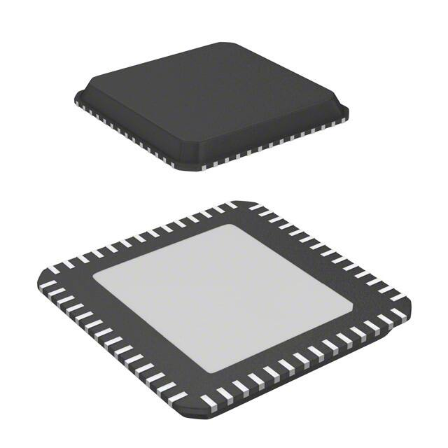


 工商网监
湘ICP备2023018690号
工商网监
湘ICP备2023018690号
