LAN8830
Gigabit Ethernet Transceiver with RGMII
Features
• Single-Chip 10/100/1000 Mbps Ethernet Transceiver Suitable for IEEE 802.3 Applications
• RGMII with 3.3V/2.5V/1.8V Tolerant I/Os
- RGMII Timing Supports On-Chip Delay According
to RGMII Version 2.0, with Programming Options
for External Delay and Making Adjustments and
Corrections to TX and RX Timing Paths
• Auto-Negotiation to Automatically Select the
Highest Link-Up Speed (10/100/1000 Mbps) and
Duplex (Half/Full)
• On-Chip Termination Resistors for the Differential
Pairs
• On-Chip LDO Controller to Support Single 3.3V
Supply Operation – Requires Only One External
FET to Generate the Core Voltage
• Jumbo Frame Support Up to 16 KB
• 125 MHz Reference Clock Output
• Energy-Detect Power-Down Mode for Reduced
Power Consumption When Cable is Not Attached
• Energy Efficient Ethernet (EEE) Support with
Low-Power Idle (LPI) Mode and Clock Stoppage
for 100BASE-TX/1000BASE-T and Transmit
Amplitude Reduction with 10BASE-Te Option
• Wake-On-LAN (WOL) Support with Robust
Custom-Packet Detection
• Programmable LED Outputs for Link, Activity, and
Speed
• LinkMD® TDR-based Cable Diagnostic to Identify
Faulty Copper Cabling
• Signal Quality Indication
• Parametric NAND Tree Support to Detect Faults
Between Chip I/Os and Board
• Loopback Modes for Diagnostics
• Automatic MDI/MDI-X Crossover to Detect and
Correct Pair Swap at All Speeds of Operation
• Automatic Detection and Correction of Pair
Swaps, Pair Skew, and Pair Polarity
• MDC/MDIO Management Interface for PHY
Register Configuration
• Interrupt Pin Option
• Power-Down and Power-Saving Modes
• Operating Voltages
extended industrial (-40°C to +105°C)
temperature ranges
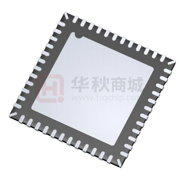
• 48-pin VQFN (7 mm × 7 mm) Package
Target Applications
•
•
•
•
•
•
•
•
•
•
•
Industrial Control
Laser/Network Printer
Network Attached Storage (NAS)
Network Server
Gigabit LAN on Motherboard (GLOM)
Broadband Gateway
Gigabit SOHO/SMB Router
IPTV
IP Set-Top Box
Game Console
Triple-Play (Data, Voice, Video) Media Center
- Core (VDD, VDDAL, VDDAL_PLL)
- VDD I/O (VDDIO): 3.3V, 2.5V, or 1.8V
- Transceiver (VDDAH): 3.3V or 2.5V
• Available in commercial (0°C to +70°C) and
2022 Microchip Technology Inc. and its subsidiaries
DS00004724A-page 1
�LAN8830
TO OUR VALUED CUSTOMERS
It is our intention to provide our valued customers with the best documentation possible to ensure successful use of your Microchip
products. To this end, we will continue to improve our publications to better suit your needs. Our publications will be refined and
enhanced as new volumes and updates are introduced.
If you have any questions or comments regarding this publication, please contact the Marketing Communications Department via
E-mail at docerrors@microchip.com. We welcome your feedback.
Most Current Data Sheet
To obtain the most up-to-date version of this data sheet, please register at our Worldwide Web site at:
http://www.microchip.com
You can determine the version of a data sheet by examining its literature number found on the bottom outside corner of any page.
The last character of the literature number is the version number, (e.g., DS30000000A is version A of document DS30000000).
Errata
An errata sheet, describing minor operational differences from the data sheet and recommended workarounds, may exist for current devices. As device/documentation issues become known to us, we will publish an errata sheet. The errata will specify the
revision of silicon and revision of document to which it applies.
To determine if an errata sheet exists for a particular device, please check with one of the following:
• Microchip’s Worldwide Web site; http://www.microchip.com
• Your local Microchip sales office (see last page)
When contacting a sales office, please specify which device, revision of silicon and data sheet (include -literature number) you are
using.
Customer Notification System
Register on our web site at www.microchip.com to receive the most current information on all of our products.
DS00004724A-page 2
2022 Microchip Technology Inc. and its subsidiaries
�LAN8830
Table of Contents
1.0 Preface ............................................................................................................................................................................................ 4
2.0 Introduction ..................................................................................................................................................................................... 7
3.0 Pin Descriptions and Configuration ................................................................................................................................................. 8
4.0 Device Connections ...................................................................................................................................................................... 21
5.0 Functional Description .................................................................................................................................................................. 24
6.0 Operational Characteristics ........................................................................................................................................................... 67
7.0 Package Outline ............................................................................................................................................................................ 90
Appendix A: Document Revision History ............................................................................................................................................ 94
The Microchip Web Site ...................................................................................................................................................................... 95
Customer Change Notification Service ............................................................................................................................................... 95
Customer Support ............................................................................................................................................................................... 95
Product Identification System ............................................................................................................................................................. 96
2022 Microchip Technology Inc. and its subsidiaries
DS00004724A-page 3
�LAN8830
1.0
PREFACE
1.1
General Terms
TABLE 1-1:
GENERAL TERMS
Term
Description
1000BASE-T
1 Gbps Ethernet over twisted pair, IEEE 802.3 compliant
100BASE-TX
100 Mbps Ethernet over twisted pair, IEEE 802.3 compliant
10BASE-T
10 Mbps Ethernet over twisted pair, IEEE 802.3 compliant
ADC
Analog-to-Digital Converter
AFE
Analog Front End
AN, ANEG
Auto-Negotiation
BYTE
8-bits
DA
Destination Address
DCQ
Dynamic Channel Quality
EEE
Energy Efficient Ethernet
FCS
Frame Check Sequence
FSM
Finite State Machine
GPIO
General Purpose I/O
HOST
External system (Includes processor, application software, etc.)
LDO
Linear Drop-Out Regulator
LFSR
Linear Feedback Shift Register
MAC
Media Access Controller
MAGJACK
Configuration strap for power modes.
MDI
Medium Dependent Interface
MDIX
Media Independent Interface with Crossover
MII
Media Independent Interface
MLT-3
Multi-Level Transmission Encoding (3-Levels). A tri-level encoding method where a
change in the logic level represents a code bit “1” and the logic output remaining at
the same level represents a code bit “0”.
N/A
Not Applicable
OTP
One Time Programmable
PCS
Physical Coding Sublayer
PLL
Phase Locked Loop
POR
Power on Reset.
RESERVED
Refers to a reserved bit field or address. Unless otherwise noted, reserved bits must
always be zero for write operations. Unless otherwise noted, values are not guaranteed when reading reserved bits. Unless otherwise noted, do not read or write to
reserved addresses.
RGMII
Reduced Gigabit Media Independent Interface
DS00004724A-page 4
2022 Microchip Technology Inc. and its subsidiaries
�LAN8830
TABLE 1-1:
GENERAL TERMS (CONTINUED)
Term
Description
SA
Source Address
SFD
Start of Frame Delimiter - The 8-bit value indicating the end of the preamble of an
Ethernet frame
SQI
Signal Quality Indicator
UDP
User Datagram Protocol - A connectionless protocol run on top of IP networks
1.2
Buffer Types
TABLE 1-2:
BUFFER TYPE DESCRIPTIONS
BUFFER
DESCRIPTION
AI
Analog input
AO
Analog output
AIO
Analog bidirectional
ICLK
Crystal oscillator input pin
OCLK
Crystal oscillator output pin
RGMII_O
RGMII compliant output
VIS
Variable voltage Schmitt-triggered input
VO5
Variable voltage output with 5 mA sink and 5 mA source
VO8
Variable voltage output with 8 mA sink and 8 mA source
VOD8
Variable voltage open-drain output with 8 mA sink
VOS8
Variable voltage open-source output with 8 mA source
VO24
Variable voltage output with 24 mA sink and 24 mA source
PU
70 KΩ (typical) internal pull-up. Unless otherwise noted in the pin description, internal pull-ups
are always enabled.
Note:
PD
70 KΩ (typical) internal pull-down. Unless otherwise noted in the pin description, internal pulldowns are always enabled.
Note:
P
Note:
Internal pull-up resistors prevent unconnected inputs from floating. Do not rely on
internal resistors to drive signals external to the device. When connected to a load
that must be pulled high, an external resistor must be added.
Internal pull-down resistors prevent unconnected inputs from floating. Do not rely on
internal resistors to drive signals external to the device. When connected to a load
that must be pulled low, an external resistor must be added.
Power pin
Digital signals are not 5V tolerant unless specified.
2022 Microchip Technology Inc. and its subsidiaries
DS00004724A-page 5
�LAN8830
1.3
1.
2.
3.
4.
Reference Documents
IEEE 802.3TM-2015 IEEE Standard for Ethernet,
http://standards.ieee.org/about/get/802/802.3.html
IEEE 802.3bwTM-2015 IEEE Standard for Ethernet Amendment 1,
https://standards.ieee.org/findstds/standard/802.3bw-2015.html
Reduced Gigabit Media Independent Interface (RGMII) Specification Version 2.0,
https://web.archive.org/web/20160303171328/http://www.hp.com/rnd/pdfs/RGMIIv2_0_final_hp.pdf
OPEN Alliance TC1 - Advanced diagnostics features for 100BASE-T1 automotive Ethernet PHYs Version 1.0
http://www.opensig.org/download/document/218/Advanced_PHY_features_for_automotive_Ethernet_V1.0.pdf
DS00004724A-page 6
2022 Microchip Technology Inc. and its subsidiaries
�LAN8830
2.0
INTRODUCTION
2.1
General Description
The LAN8830 is a completely integrated triple-speed (10BASE-T/100BASE-TX/1000BASE-T) Ethernet physical-layer
transceiver for transmission and reception of data on standard CAT-5 as well as CAT-5e and CAT-6 unshielded twisted
pair (UTP) cables.
The LAN8830 provides the Reduced Gigabit Media Independent Interface (RGMII) for direct connection to RGMII MACs
in Gigabit Ethernet processors and switches for data transfer at 10/100/1000 Mbps.
The LAN8830 reduces board cost and simplifies board layout by using on-chip termination resistors for the four differential pairs and by integrating an LDO controller to drive a low-cost MOSFET to supply the core voltage.
The LAN8830 offers diagnostic features to facilitate system bring-up and debugging in production testing and in product
deployment. Parametric NAND tree support enables fault detection between LAN8830 I/Os and the board. The
LinkMD® TDR-based cable diagnostic identifies faulty copper cabling. Remote, external, and local loopback functions
verify analog and digital data paths.
The LAN8830 is available in a 48-pin, RoHS Compliant VQFN package.
FIGURE 2-1:
SYSTEM BLOCK DIAGRAM
10/100/1000Mbps
RGMII
Ethernet MAC
LAN8830
MDC/MDIO
MANAGEMENT
INT_N /
PME_N /
LEDs /
GPIOs
SYSTEM POWER CIRCUIT /
INTERUPT CONTROLLER /
LEDs / GPIOs
MAGNETICS
RGMII
ON-CHIP TERMINATION
RESISTORS
CRYSTAL
RJ-45
CONNECTOR
MEDIA TYPES
10BASE-T
100BASE-TX
1000BASE-T
LDO
CONTROLLER
VIN 3.3V,
2.5V
2022 Microchip Technology Inc. and its subsidiaries
VOUT
DS00004724A-page 7
�LAN8830
3.0
PIN DESCRIPTIONS AND CONFIGURATION
3.1
Pin Assignments
ISET
VDDAL_PLL
XI
XO
LDO_O
RESET_N
CLK125_NDO/GPIO6/LED_MODE
VDDIO
VDD
INT_N/GPIO5
MDIO
MDC
47
46
45
44
43
42
41
40
39
38
37
PIN ASSIGNMENTS (TOP VIEW)
48
FIGURE 3-1:
VDDAH
1
36
RXC/MODE4
TXRXP_A
2
35
VDDIO
TXRXM_A
3
34
RX_CTL/CLK125_EN
VDDAL
4
33
RXD0/MODE0
TXRXP_B
5
32
RXD1/MODE1
TXRXM_B
6
31
VDD
30
RXD2/MODE2
LAN8830
48 -VQFN
TXRXP_C
7
TXRXM_C
8
29
RXD3/MODE3
VDDAL
9
28
VDDIO
TXRXP_D
10
27
VDD
TXRXM_D
11
26
TX_CTL
VDDAH
12
25
TXC
( To p V i ew )
P_VSS
13
14
15
16
17
18
19
20
21
22
23
24
LED5/GPIO4/ALLPHYAD/LEDPOL5
LED4/GPIO3/MAGJACK/LEDPOL4
LED3/GPIO2/PHYAD2/LEDPOL3
LED2/GPIO1/PHYAD1/LEDPOL2
VDDIO
LED1/GPIO0/PHYAD0/LEDPOL1
TXD0
TXD1
TXD2
TXD3
VDD
VDDIO
Connect exposed pad to ground with a via field
Note: Exposed pad (P_VSS) on bottom of package must be connected to ground with a via field
Note: Configuration strap inputs are indicated with an underline
Note: This pinout is preliminary and not intended for schematic use
Note: PME_N is not shown since it can map to various GPIO pins
DS00004724A-page 8
2022 Microchip Technology Inc. and its subsidiaries
�LAN8830
TABLE 3-1:
Pin
Num
LAN8830 PIN ASSIGNMENTS
Pin Name
Pin
Num
1
VDDAH
25
TXC
2
TXRXP_A
26
TX_CTL
3
TXRXM_A
27
VDD
Pin Name
4
VDDAL
28
VDDIO
5
TXRXP_B
29
RXD3/MODE3
6
TXRXM_B
30
RXD2/MODE2
7
TXRXP_C
31
VDD
8
TXRXM_C
32
RXD1/MODE1
9
VDDAL
33
RXD0/MODE0
10
TXRXP_D
34
RX_CTL/CLK125_EN
11
TXRXM_D
35
VDDIO
12
VDDAH
36
RXC/MODE4
13
LED5/GPIO4/ALLPHYAD/LEDPOL5
37
MDC
14
LED4/GPIO3/MAGJACK/LEDPOL4
38
MDIO
15
LED3/GPIO2/PHYAD2/LEDPOL3
39
INT_N/GPIO5
16
LED2/GPIO1/PHYAD1/LEDPOL2
40
VDD
17
VDDIO
41
VDDIO
18
LED1/GPIO0/PHYAD0/LEDPOL1
42
CLK125_NDO/GPIO6/LED_MODE
19
TXD0
43
RESET_N
20
TXD1
44
LDO_O
21
TXD2
45
XO
22
TXD3
46
XI
23
VDD
47
VDDAL_PLL
24
VDDIO
48
ISET
Exposed Pad (P_VSS) must be connected to ground.
2022 Microchip Technology Inc. and its subsidiaries
DS00004724A-page 9
�LAN8830
3.2
Pin Descriptions
This section contains descriptions of the various LAN8830 pins. The “_N” symbol in the signal name indicates that the
active, or asserted, state occurs when the signal is at a low voltage level. For example, RESET_N indicates that the
reset signal is active low. When “_N” is not present after the signal name, the signal is asserted when at the high voltage
level.
The pin function descriptions have been broken into functional groups as follows:
•
•
•
•
•
•
•
Analog Front End
RGMII Interface
Crystal
Miscellaneous
Alternate Functions
Strap Inputs
I/O Power, Core Power and Ground
TABLE 3-2:
ANALOG FRONT END
Name
Symbol
Buffer
Type
Ethernet TX/RX
Positive Channel
A
TXRXP_A
AIO
Description
Media Dependent Interface[0], positive signal of differential
pair
1000BT mode: TXRXP_A corresponds to BI_DA+.
Ethernet TX/RX
Negative Channel
A
TXRXM_A
AIO
10BT/100BTX mode: TXRXP_A is the positive transmit signal
(TX+) for MDI configuration and the positive receive signal
(RX+) for MDI-X configuration, respectively.
Media Dependent Interface[0], negative signal of differential
pair
1000BT mode: TXRXM_A corresponds to BI_DA-.
Ethernet TX/RX
Positive Channel
B
TXRXP_B
AIO
10BT/100BTX mode: TXRXM_A is the negative transmit signal (TX-) for MDI configuration and the negative receive signal
(RX-) for MDI-X configuration, respectively.
Media Dependent Interface[1], positive signal of differential
pair
1000BT mode: TXRXP_B corresponds to BI_DB+.
Ethernet TX/RX
Negative Channel
B
TXRXM_B
AIO
10BT/100BTX mode: TXRXP_B is the positive receive signal
(RX+) for MDI configuration and the positive transmit signal
(TX+) for MDI-X configuration, respectively.
Media Dependent Interface[1], negative signal of differential
pair
1000BT mode: TXRXM_B corresponds to BI_DB-.
10BT/100BTX mode: TXRXP_B is the negative receive signal
(RX-) for MDI configuration and the negative transmit signal
(TX-) for MDI-X configuration, respectively.
DS00004724A-page 10
2022 Microchip Technology Inc. and its subsidiaries
�LAN8830
TABLE 3-2:
ANALOG FRONT END (CONTINUED)
Name
Symbol
Buffer
Type
Ethernet TX/RX
Positive Channel
C
TXRXP_C
AIO
Description
Media Dependent Interface[2], positive signal of differential
pair
1000BT mode: TXRXP_C corresponds to BI_DC+.
Ethernet TX/RX
Negative Channel
C
TXRXM_C
AIO
10BT/100BTX mode: TXRXP_C is not used.
Media Dependent Interface[2], negative signal of differential
pair
1000BT mode: TXRXM_C corresponds to BI_DC-
Ethernet TX/RX
Positive Channel
D
TXRXP_D
AIO
10BT/100BTX mode: TXRXM_C is not used.
Media Dependent Interface[3], positive signal of differential
pair
1000BT mode: TXRXP_D corresponds to BI_DD+.
Ethernet TX/RX
Negative Channel
D
TXRXM_D
AIO
10BT/100BTX mode: TXRXP_D is not used.
Media Dependent Interface[3], negative signal of differential
pair
1000BT mode: TXRXM_D corresponds to BI_DD-.
10BT/100BTX mode: TXRXM_D is not used.
2022 Microchip Technology Inc. and its subsidiaries
DS00004724A-page 11
�LAN8830
TABLE 3-3:
RGMII INTERFACE
Buffer
Type
Name
Symbol
Transmit Data
TXD3
TXD2
TXD1
TXD0
TX_CTL
VIS
The MAC transmits data to the PHY using these signals.
VIS
TXC
VIS
Indicates both the transmit data enable (TXEN) and transmit
error (TXER) functions per the RGMII specification.
Used to latch data from the MAC into the PHY in RGMII mode.
Transmit Control
RGMII Transmit
Clock
Receive Data
RXD3
RXD2
RXD1
RXD0
Receive Control
RX_CTL
RGMII Receive
Clock
RXC
Description
1000BASE-T: 125MHz
100BASE-TX: 25MHz
10BASE-T: 2.5MHz
RGMII_O The PHY transfers data to the MAC using these signals.
The PHY’s link status (speed, duplex and link) are indicated on
these signals whenever Normal Data, Data Error, Carrier
Extend, Carrier Sense, False Carrier or Lower Power Idle are
not present.
RGMII_O Indicates both the receive data valid (RXDV) and receive error
(RXER) functions per the RGMII specification.
RGMII_O Used to transfer data from the PHY to the MAC in RGMII
mode.
1000BASE-T: 125MHz
100BASE-TX: 25MHz
10BASE-T: 2.5MHz
TABLE 3-4:
CRYSTAL
Name
Symbol
BUFFER
TYPE
Crystal Input
XI
ICLK
DESCRIPTION
When using a 25MHz crystal, this input is connected to one
lead of the crystal.
When using an clock source, this is the input from the oscillator.
Note:
Crystal Output
XO
OCLK
The crystal or oscillator should have a tolerance of
±50ppm.
When using a 25MHz crystal, this output is connected to one
lead of the crystal.
When using an external oscillator, this pin is not connected.
DS00004724A-page 12
2022 Microchip Technology Inc. and its subsidiaries
�LAN8830
TABLE 3-5:
MISCELLANEOUS
Name
Symbol
Indicator LEDs
LED5
LED4
LED3
LED2
LED1
General Purpose
I/O
Management
Interface Data
Management
Interface Clock
PHY Interrupt
GPIO6
GPIO5
GPIO4
GPIO3
GPIO2
GPIO1
GPIO0
MDIO
MDC
INT_N
Buffer
Type
VO10/
VOD10/
VOS10
VIS/
VO10/
VOD10
(PU)
Description
Programmable LED outputs.
The polarity of the pin depends upon the corresponding LED
Polarity bit in the Output Control Register.
The buffer type (push-pull or open-drain/open-source)
depends on the setting of the corresponding LED Buffer Type
bit in the Output Control Register. This polarity then determines open-drain (active low) and open-source (active high).
General purpose I/O
The buffer type (push-pull or open-drain/open-source), direction, and pull-up depend on the settings in the GPIO registers.
GPIOs are shared with various pins.
VIS/
VO10
VOD10
(PU)
VIS
(PU)
VO10/
VOD10
This is the management data from/to the MAC.
Note:
An external pull-up resistor to VDDIO in the range of
1.0 kΩ to 4.7 kΩ is required. (1.0 kΩ for high-speed
MDIO operation).
The buffer type (push-pull or open-drain/open-source)
depends on the setting of the MDIO Buffer Type bit in the Output Control Register.
This is the management clock input from the MAC.
Programmable interrupt output.
The buffer type (push-pull or open-drain) depends on the setting of the INT Buffer Type bit in the Output Control Register
and defaults to open-drain.
The polarity depends on the setting of the Intr Polarity Invert bit
in the Control Register and defaults to active low.
Note:
CLK125 MHz
CLK125_NDO
If the buffer type is set to open-drain, the polarity is
forced to be active low.
VIS/VO10 125 MHz clock output.
This pin provides a 125 MHz reference clock output option for
use by the MAC.
This pin may also provide a 125 MHz clock output synchronous to the receive data for use in Synchronous Ethernet
(SyncE) applications.
System Reset
RESET_N
VIS
(PU)
Chip reset (active low).
Hardware pin configurations are strapped-in at the de-assertion (rising edge) of RESET_N.
2022 Microchip Technology Inc. and its subsidiaries
DS00004724A-page 13
�LAN8830
TABLE 3-5:
MISCELLANEOUS (CONTINUED)
Name
Symbol
Buffer
Type
LDO Controller
Output
LDO_O
AO
Description
On-chip core voltage LDO controller output.
This pin drives the input gate of a P-channel MOSFET to generate the chip’s core voltages.
Note:
PHY Bias Resistor
TABLE 3-6:
ISET
AI
If the system provides the core voltage, this pin is not
used and can be left unconnected.
This pin should be connected to ground through a 6.04KΩ 1%
resistor.
ALTERNATE FUNCTIONS
Name
Symbol
Power Management Event
PME_N
Buffer
Type
VO10/
VOD10/
Description
Programmable PME_N output.
When asserted, this pin signals that a WOL event has
occurred.
PME_N can be mapped to various GPIO pins.
The buffer type (push-pull or open-drain) depends on the setting of the corresponding GPIO Buffer Type (GPIO_BUF) bit in
the General Purpose IO Buffer Type Register (GPIO_BUF).
The polarity is set by the PME Polarity bit in the Output Control
Register.
TABLE 3-7:
STRAP INPUTS
Name
Symbol
Buffer
Type
MagJack
MAGJACK
VIS
PHY Address
PHYAD2
PHYAD1
PHYAD0
VIS
DS00004724A-page 14
Description
The MAGJACK strap-in pin is sampled and latched at powerup/reset and is used to set various registers for MagJack operation as follows:
0 = normal register settings
1 = MagJack register settings
See Section 3.3, "Configuration Straps" for more information.
The PHY address, PHYAD[2:0], is sampled and latched at
power-up/reset and is configurable to any value from 0 to 7h.
Each PHY address bit is configured as follows:
Pulled-up = 1
Pulled-down = 0
See Section 3.3, "Configuration Straps" for more information.
2022 Microchip Technology Inc. and its subsidiaries
�LAN8830
TABLE 3-7:
STRAP INPUTS (CONTINUED)
Buffer
Type
Name
Symbol
LED Polarity
LEDPOL5
LEDPOL4
LEDPOL3
LEDPOL2
LEDPOL1
VIS
ALLPHYAD
VIS
All PHY Address
Enable
Description
Since the LED pins are shared with configuration straps, the
default polarity of the LED pins is determined during strap
loading.
If the strap value on a pin is a 0, the LED is set as active high
(LEDPOL=1), since it is assumed that a LED to ground is used
as the pull-down.
If the strap value on a pin is 1, the LED is set as active low
(LEDPOL=0),
since it is assumed that a LED to VDDIO is used as the pullup.
See Section 3.3, "Configuration Straps" for more information.
The ALLPHYAD strap-in pin is sampled and latched at powerup/reset and are defined as follows:
0 = PHY will respond to PHY address 0 as well as it’s assigned
PHY address
1 = PHY will respond to only it’s assigned PHY address
Note:
Device Mode
125MHz Output
Clock Enable
LED Mode
This strap input is inverted compared to the All
PHYAD Enable register bit.
See Section 3.3, "Configuration Straps" for more information.
The MODE[4:0] strap-in pins are sampled and latched at
power-up/reset and are defined in Section 3.3.1, "Device Mode
Select (MODE[4:0])".
See Section 3.3, "Configuration Straps" for more information.
MODE4
MODE3
MODE2
MODE1
MODE0
CLK125_EN
VIS
VIS
CLK125_EN is sampled and latched at power-up/reset and is
defined as follows:
0 = Disable 125 MHz clock output
1 = Enable 125 MHz clock output
CLK125_NDO provides the 125 MHz reference clock output
option for use by the MAC.
See Section 3.3, "Configuration Straps" for more information.
LED_MODE
VIS
LED_MODE is sampled and latched at power-up/reset and is
defined as follows:
0 = Tri-color-LED mode
1 = Individual-LED mode
See Section 3.3, "Configuration Straps" for more information.
2022 Microchip Technology Inc. and its subsidiaries
DS00004724A-page 15
�LAN8830
TABLE 3-8:
I/O POWER, CORE POWER AND GROUND
Name
Symbol
Buffer
Type
+2.5/3.3V
Analog Power
Supply
VDDAH
P
+2.5/3.3V analog power supply VDD
+1.1V Analog
Power Supply
VDDAL
P
+1.1V analog power supply VDD
+1.1V Analog
PLL Power
Supply
VDDAL_PLL
P
+1.1V analog PLL power supply VDD
+3.3/2.5/1.8V
Variable I/O
Power Supply
Input
VDDIO
P
+3.3/2.5/1.8V variable I/O digital power supply VDD_IO
+1.1V Digital
Core Power
Supply Input
VDD
P
+1.1V digital core power supply input
Paddle Ground
P_VSS
GND
DS00004724A-page 16
Description
Common ground. This exposed paddle must be connected to
the ground plane with a via array.
2022 Microchip Technology Inc. and its subsidiaries
�LAN8830
3.3
Configuration Straps
Configuration straps allow various features of the device to be automatically configured to user defined values. Configuration straps are latched upon the release of pin reset (RESET_N). Configuration straps do not include internal resistors and require the use of external resistors.
Note:
The system designer must ensure that configuration strap pins meet timing requirements. The system
designer must guarantee that configuration strap pins meet the timing requirements specified in Section
6.6.3, "Reset Pin Configuration Strap Timing". If configuration strap pins are not at the correct voltage level
prior to being latched, the device may capture incorrect strap values.
Note:
When externally pulling configuration straps high, the strap should be tied to VDDIO.
APPLICATION NOTE: All straps should be pulled-up or pulled-down externally on the PCB to enable the desired
operational state.
3.3.1
DEVICE MODE SELECT (MODE[4:0])
The MODE[4:0] configuration straps select the device mode as follows:
Note:
MODE[4:0] definitions are preliminary and subject to change.
Note:
1000BT Half Duplex is not advertised in any of the below device modes.
TABLE 3-9:
DEVICE MODE SELECTIONS
Test Modes
MODE
Mode
[4:0]
00010
00011
00100
00101
00110
00111
RESERVED
RESERVED
NAND tree mode
RESERVED
RESERVED
Device power down mode
Functional Modes
Power Down
01000 Software Power Down PLL Enabled
01001 Software Power Down PLL Disabled
Auto-Negotiation Disabled, Auto MDIX Disabled, EEE Disabled
01010
01011
01100
01101
1000FD Host
100FD
100HD
1000FD Client
*Legend:
1000FD = 1000BASE-T Full Duplex
100FD = 100BASE-TX Full Duplex
100HD = 100BASE-TX Half Duplex
10FD = 10BASE-T Full Duplex
10HD = 10BASE-T Half Duplex
2022 Microchip Technology Inc. and its subsidiaries
DS00004724A-page 17
�LAN8830
TABLE 3-9:
DEVICE MODE SELECTIONS (CONTINUED)
Auto-Negotiation Enabled, Auto MDIX Enabled, EEE Disabled, Asym & Sym Pause Advertised
Auto-Negotiation Advertisement
1000BT
FD
10000 1000FD Single Port
100FD/HD
10FD/HD
10001 1000FD Multi Port
100FD/HD
10FD/HD
10010 1000FD Single Port
10011 1000FD Multi Port
10100 100FD/HD
10101 100FD
10110 100HD
10111 100FD/HD
10FD/HD
100BTX
Single
EEE
/ Multi
FD
HD
10BT
EEE
FD
HD
Asym 10BT AMDIX
/ Sym cat3/5
Pause
X
S
X
X
X
X
X
cat3
X
X
M
X
X
X
X
X
cat3
X
X
X
S
M
X
X
X
X
X
X
X
na
na
na
na
na
cat3
X
X
X
X
X
X
X
X
X
X
X
X
X
Auto-Negotiation Enabled, Auto MDIX Enabled, EEE Enabled, Asym & Sym Pause Advertised
Auto-Negotiation Advertisement
1000BT
FD
11000 1000FD Single Port
100FD/HD
10FD/HD
11001 1000FD Multi Port
100FD/HD
10FD/HD
11010 1000FD Single Port
11011 1000FD Multi Port
11100 100FD/HD
11101 100FD
11111 100FD/HD
10FD/HD
100BTX
Single
EEE
/ Multi
10BT
FD
HD
EEE
FD
HD
Asym 10BT AMDIX
/ Sym cat3/5
Pause
X
S
X
X
X
X
X
X
X
cat5
X
X
M
X
X
X
X
X
X
X
cat5
X
X
X
S
M
X
X
X
X
X
X
X
X
na
na
na
na
cat5
X
X
X
X
X
X
X
X
X
X
X
X
X
X
RESERVED
00000
00001
01101
01110
01111
11110
RESERVED
RESERVED
RESERVED
RESERVED
RESERVED
RESERVED
*Legend:
1000FD = 1000BASE-T Full Duplex
100FD = 100BASE-TX Full Duplex
100HD = 100BASE-TX Half Duplex
10FD = 10BASE-T Full Duplex
10HD = 10BASE-T Half Duplex
DS00004724A-page 18
2022 Microchip Technology Inc. and its subsidiaries
�LAN8830
3.3.2
MAGJACK (MAGJACK)
The MAGJACK configuration straps sets the value of MMD28 registers 13h through 1Eh for compatibility with MagJack
RJ-45s with common center-taps.
3.3.3
PHY ADDRESS (PHYAD[2:0])
The PHYAD[2:0] configuration straps set the value of the PHY’s management address.
3.3.4
ALL PHYs ADDRESS (ALLPHYAD)
The ALLPHYAD configuration strap sets the default of the All-PHYAD Enable bit in the Common Control Register which
enables (pulled-down) or disables (pulled-up) the PHY’s ability to respond to PHY address 0 as well as its assigned PHY
address.
Note:
3.3.5
This strap input is inverted compared to the register bit.
125MHZ OUTPUT CLOCK ENABLE (CLK125_EN)
The CLK125_EN configuration strap enables the 125 MHz clock output onto the CLK125_NDO pin (pulled-up).
The output clock defaults to a locally generated 125MHz clock.
3.3.6
LED MODE SELECT (LED_MODE)
The LED_MODE configuration strap selects between Individual-LED (pulled-up) or Tri-color-LED (pulled-down) modes.
3.3.7
LED POLARITY (LEDPOL[5:1])
The LEDPOL[5:1] configuration straps set the default polarity of the LED pins.
When a LED pin is used as a function mode strap (for example a PHY address bit), it is difficult to strap in a low value
when a (active low) LED is connected via a resistor to VDDIO. A secondary pull-down resistor is needed to provide a
low level during strap load time. When the LED is lit (pin driven low), the pull-down resistor is inconsequential. However,
when the LED is not lit (pin driven high), the device drives wasted current, on the order of 3ma, through this resistor.
This is especially important during power saving modes with multiple LEDs. This situation is shown in Figure 3-2.
FIGURE 3-2:
LOW STRAP ON LED PIN
LED output On
Functional Strap = 0
LED Output Active Low
VDDIO
VDDIO
220
strap resistor
sized to 1K
ensure a low
level during
strap load
LED output Off
220
LED / strap pin
(driving 0)
2022 Microchip Technology Inc. and its subsidiaries
strap resistor
sized to 1K
ensure a low
level during
strap load
LED / strap pin
(driving 1)
DS00004724A-page 19
�LAN8830
To avoid this, the default LED pin polarity, shown in the Strap Status Register, is automatically selected based on the
inverse of the strap value. A LED, via a resistor, is then used as a pull-up, or as a pull-down.This is shown in Figure 3-3.
FIGURE 3-3:
STRAP ON LED WITH POLARITY
Functional Strap = 1
LED output = Active Low (LEDPOL strap = 1)
Functional Strap = 0
LED output = Active High (LEDPOL strap = 1)
VDDIO
LED / strap pin
supplemental
resistor to
ensure a valid
low level
during strap
load
220
220
LED / strap pin
3.4
Pin Alternate Functions
Various pins may be configured to carry alternate functions if the primary function is not required by the application:
• LEDs 1-5 may be individually configured as GPIO0-4 by setting the corresponding GPIO Enable (GPIO_EN) bits
in the General Purpose IO Enable Register (GPIO_EN).
• INT_N may be configured as GPIO5 by setting the corresponding GPIO Enable (GPIO_EN) bit in the General
Purpose IO Enable Register (GPIO_EN).
• CLK125_NDO may be configured as GPIO6 by setting the corresponding GPIO Enable (GPIO_EN) bit in the
General Purpose IO Enable Register (GPIO_EN).
• PME_N may be mapped to any enabled GPIO by setting the corresponding bits in the General Purpose IO Data
Select 1 Register (GPIO_DATA_SEL1) or the General Purpose IO Data Select 2 Register (GPIO_DATA_SEL2).
DS00004724A-page 20
2022 Microchip Technology Inc. and its subsidiaries
�LAN8830
4.0
DEVICE CONNECTIONS
4.1
Voltage Regulator
In order to facilitate ease of integration, this device includes an LDO controller for use with an external MOSFET to generate the core voltage supply.
4.1.1
MOSFET SELECTION
The selected MOSFET should exceed the following minimum requirements:
•
•
•
•
•
P-channel
500 mA (continuous current)
3.3V or 2.5V (source – input voltage)
1.1V (drain – output voltage)
VGS in the range of:
- (–1.2V to –1.5V) @ 500 mA or 3.3V source voltage
- (–1.0V to –1.1V) @ 500 mA for 2.5V source voltage
The VGS for the MOSFET needs to be operating in the constant current saturated region, and not towards the VGS(th),
the threshold voltage for the cut-off region of the MOSFET.
Refer to Table 6-10 for the LDO controller output driving range to the gate input of the MOSFET.
A 47µF electrolytic capacitor between 3.3V/2.5V source and ground is required. A 47µF electrolytic capacitor between
core voltage and ground is required for proper LDO operation.
4.1.2
LDO DISABLE
The LDO controller can be disabled by setting the LDO Enable bit in Analog Control Register 11. An external source of
1.1V is necessary for operation in this case.
4.2
Power Connectivity
This section details the power connectivity of the device in the following modes of operation:
• Power Connectivity with Internal LDO Controller
• Power Connectivity with External 1.1V Power Supply
2022 Microchip Technology Inc. and its subsidiaries
DS00004724A-page 21
�LAN8830
4.2.1
POWER CONNECTIVITY WITH INTERNAL LDO CONTROLLER
FIGURE 4-1:
POWER CONNECTIVITY WITH INTERNAL LDO CONTROLLER
+2.5V,
+3.3V
+
+
100K
LDO_O
LDO
+1.8V,
+2.5V,
+3.3V
VDDIO
(5 pins)
IO Pads
VDD
(3 pins)
Digital
PLL
Analog
VDDAL_PLL
(1 pin)
VDDAL
(4 pins)
+3.3V,
+2.5V
Bandgap and Osc
P_VSS
(exposed paddle)
VDDAH
(3 pins)
Notes: Bypass and bulk caps as needed for PCB.
Electrolytic capacitor required on MOSFET output.
Ferrites on VDDAL and VDDAL_PLL may be combined.
DS00004724A-page 22
2022 Microchip Technology Inc. and its subsidiaries
�LAN8830
4.2.2
POWER CONNECTIVITY WITH EXTERNAL 1.1V POWER SUPPLY
FIGURE 4-2:
POWER CONNECTIVITY WITH EXTERNAL 1.1V POWER SUPPLY
+1.1V
NC
LDO_O
LDO
+1.8V,
+2.5V,
+3.3V
VDDIO
(5 pins)
IO Pads
VDD
(3 pins)
Digital
PLL
Analog
VDDAL_PLL
(1 pin)
VDDAL
(2 pins)
+3.3V,
+2.5V
Bandgap and Osc
P_VSS
(exposed paddle)
VDDAH
(2 pins)
Notes: Bypass and bulk caps as needed for PCB.
Ferrites on VDDAL and VDDAL_PLL may be combined.
2022 Microchip Technology Inc. and its subsidiaries
DS00004724A-page 23
�LAN8830
5.0
FUNCTIONAL DESCRIPTION
The LAN8830 is a completely integrated triple-speed (10BASE-T/100BASE-TX/1000BASE-T) Ethernet physical layer
transceiver solution for transmission and reception of data over a standard CAT-5, as well as CAT-5e and CAT-6,
unshielded twisted pair (UTP) cables.
The device reduces board cost and simplifies board layout by using on-chip termination resistors for the four differential
pairs and by integrating an LDO controller to drive a low-cost MOSFET to supply the core voltage.
On the copper media interface, the device can automatically detect and correct for differential pair misplacements and
polarity reversals, and correct propagation delays and re-sync timing between the four differential pairs, as specified in
the IEEE 802.3 standard for 1000BASE-T operation.
The LAN8830 provides the RGMII interface for connection to RGMII MACs in Gigabit Ethernet processors and switches
for data transfer at 10/100/1000 Mbps.
Figure 5-1 shows a high-level block diagram of the LAN8830.
FIGURE 5-1:
LAN8830 BLOCK DIAGRAM
PMA
TX10/100/1000
CLOCK
RESET
CONFIGURATIONS
PMA
RX1000
PCS 1000
MEDIA
INTERFACE
PMA
RX100
PCS 100
PMA
RX10
PCS 10
AUTONEGOTIATION
5.1
5.1.1
RGMII
INTERFACE
LED
DRIVERS
10BASE-T/100BASE-TX Transceiver
100BASE-TX TRANSMIT
The 100BASE-TX transmit function performs parallel-to-serial conversion, 4B/5B coding, scrambling, NRZ-to-NRZI conversion, and MLT-3 encoding and transmission.
The circuitry starts with a parallel-to-serial conversion, which converts the MII data from the MAC into a 125 MHz serial
bit stream. The data and control stream is then converted into 4B/5B coding, followed by a scrambler. The serialized
data is further converted from NRZ-to-NRZI format, and then transmitted in MLT-3 current output. The output current is
set by an external 6.04 kΩ 1% resistor for the 1:1 transformer ratio.
The output signal has a typical rise/fall time of 4 ns and complies with the ANSI TP-PMD standard regarding amplitude
balance, and overshoot. The wave-shaped 10BASE-T output is also incorporated into the 100BASE-TX transmitter.
5.1.2
100BASE-TX RECEIVE
The 100BASE-TX receiver function performs adaptive equalization, DC restoration, MLT-3-to-NRZI conversion, data
and clock recovery, NRZI-to-NRZ conversion, de-scrambling, 4B/5B decoding, and serial-to-parallel conversion.
DS00004724A-page 24
2022 Microchip Technology Inc. and its subsidiaries
�LAN8830
The receiving side starts with the equalization filter to compensate for inter-symbol interference (ISI) over the twisted
pair cable. Because the amplitude loss and phase distortion are a function of the cable length, the equalizer must adjust
its characteristics to optimize performance. In this design, the variable equalizer makes an initial estimation based on
comparisons of incoming signal strength against some known cable characteristics, then tunes itself for optimization.
This is an ongoing process and self-adjusts against environmental changes such as temperature variations.
Next, the equalized signal goes through a DC-restoration and data-conversion block. The DC-restoration circuit compensates for the effect of baseline wander and improves the dynamic range. The differential data conversion circuit converts the MLT-3 format back to NRZI. The slicing threshold is also adaptive.
The clock-recovery circuit extracts the 125 MHz clock from the edges of the NRZI signal. This recovered clock is then
used to convert the NRZI signal into the NRZ format. This signal is sent through the de-scrambler followed by the 4B/
5B decoder. Finally, the NRZ serial data is converted to the RGMII format and provided as the input data to the MAC.
5.1.3
SCRAMBLER/DE-SCRAMBLER (100BASE-TX ONLY)
The purpose of the scrambler is to spread the power spectrum of the signal to reduce electromagnetic interference (EMI)
and baseline wander. Transmitted data is scrambled using an 11-bit wide linear feedback shift register (LFSR). The
scrambler generates a 2047-bit non-repetitive sequence, then the receiver de-scrambles the incoming data stream
using the same sequence as at the transmitter.
5.1.4
10BASE-T TRANSMIT
The 10BASE-T output drivers are incorporated into the 100BASE-TX drivers to allow for transmission with the same
magnetic. The drivers perform internal wave-shaping and pre-emphasis, and output signals with typical amplitude of
2.5V peak for standard 10BASE-T mode and 1.75V peak for energy-efficient 10BASE-Te mode. The 10BASE-T/
10BASE-Te signals have harmonic contents that are at least 31 dB below the fundamental frequency when driven by
an all-ones Manchester-encoded signal.
5.1.5
10BASE-T RECEIVE
On the receive side, input buffer and level-detecting squelch circuits are used. A differential input receiver circuit and a
phase-locked loop (PLL) perform the decoding function. The Manchester-encoded data stream is separated into clock
signal and NRZ data. A squelch circuit rejects signals with levels less than 300 mV or with short pulse widths to prevent
noises at the receive inputs from falsely triggering the decoder. When the input exceeds the squelch limit, the PLL locks
onto the incoming signal and the device decodes a data frame. The receiver clock is maintained active during idle periods between receiving data frames.
The device removes all 7 bytes of the preamble and presents the received frame starting with the SFD (start of frame
delimiter) to the MAC.
Auto-polarity correction is provided for the receiving differential pair to automatically swap and fix the incorrect +/– polarity wiring in the cabling.
2022 Microchip Technology Inc. and its subsidiaries
DS00004724A-page 25
�LAN8830
5.2
1000BASE-T Transceiver
The 1000BASE-T transceiver is based-on a mixed-signal/digital-signal processing (DSP) architecture, which includes
the analog front-end, digital channel equalizers, trellis encoders/decoders, echo cancelers, cross-talk cancelers, precision clock recovery scheme, and power-efficient line drivers.
Figure 5-2 shows a high-level block diagram of a single channel of the 1000BASE-T transceiver for one of the four differential pairs.
FIGURE 5-2:
1000BASE-T BLOCK DIAGRAM - SINGLE CHANNEL
XTAL
OTHER
CHANNELS
CLOCK
GENERATION
TX
SIGNAL
SIDE -STREAM
SCRAMBLER
&
SYMBOL ENCODER
TRANSMIT
BLOCK
PCS STATE
MACHINES
LED DRIVER
NEXT
CANCELLER
NEXT
Canceller
NEXT Canceller
ECHO
CANCELLER
ANALOG
HYBRID
PAIR SWAP
&
ALIGN UNIT
BASELINE
WANDER
COMPENSATION
AGC
RXADC
FFE
+
DESCRAMBLER
+
DECODER
SLICER
RX
SIGNAL
CLOCK & PHASE
RECOVERY
AUTO NEGOTIATION
DFE
MII
REGISTERS
MII
MANAGEMENT
CONTROL
PMA STATE
MACHINES
5.2.1
ANALOG ECHO-CANCELLATION CIRCUIT
In 1000BASE-T mode, the analog echo-cancellation circuit helps to reduce the near-end echo. This analog hybrid circuit
relieves the burden of the ADC and the adaptive equalizer.
This circuit is disabled in 10BASE-T/100BASE-TX mode.
5.2.2
AUTOMATIC GAIN CONTROL (AGC)
In 1000BASE-T mode, the automatic gain control (AGC) circuit provides initial gain adjustment to boost up the signal
level. This pre-conditioning circuit is used to improve the signal-to-noise ratio of the receive signal.
5.2.3
ANALOG-TO-DIGITAL CONVERTER (ADC)
In 1000BASE-T mode, the analog-to-digital converter (ADC) digitizes the incoming signal. ADC performance is essential to the overall performance of the transceiver.
This circuit is disabled in 10BASE-T/100BASE-TX mode.
5.2.4
TIMING RECOVERY CIRCUIT
In 1000BASE-T mode, the mixed-signal clock recovery circuit together with the digital phase-locked loop is used to
recover and track the incoming timing information from the received data. The digital phase-locked loop has very low
long-term jitter to maximize the signal-to-noise ratio of the receive signal.
DS00004724A-page 26
2022 Microchip Technology Inc. and its subsidiaries
�LAN8830
The 1000BASE-T slave PHY must transmit the exact receive clock frequency recovered from the received data back to
the 1000BASE-T master PHY. Otherwise, the master and slave will not be synchronized after long transmission. This
also helps to facilitate echo cancellation and NEXT removal.
5.2.5
ADAPTIVE EQUALIZER
In 1000BASE-T mode, the adaptive equalizer provides the following functions:
• Detection for partial response signaling
• Removal of NEXT and ECHO noise
• Channel equalization
Signal quality is degraded by residual echo that is not removed by the analog hybrid because of impedance mismatch.
The device uses a digital echo canceler to further reduce echo components on the receive signal.
In 1000BASE-T mode, data transmission and reception occurs simultaneously on all four pairs of wires (four channels).
This results in high-frequency cross-talk coming from adjacent wires. The device uses three NEXT cancelers on each
receive channel to minimize the cross-talk induced by the other three channels.
In 10BASE-T/100BASE-TX mode, the adaptive equalizer needs only to remove the inter-symbol interference and
recover the channel loss from the incoming data.
5.2.6
TRELLIS ENCODER AND DECODER
In 1000BASE-T mode, the transmitted 8-bit data is scrambled into 9-bit symbols and further encoded into 4D-PAM5
symbols. The initial scrambler seed is determined by the specific PHY address to reduce EMI when more than one
device is used on the same board. On the receiving side, the idle stream is examined first. The scrambler seed, pair
skew, pair order, and polarity must be resolved through the logic. The incoming 4D-PAM5 data is then converted into 9bit symbols and de-scrambled into 8-bit data.
5.3
Auto MDI/MDI-X
The Automatic MDI/MDI-X feature eliminates the need to determine whether to use a straight cable or a crossover cable
between the device and its link partner. This auto-sense function detects the MDI/MDI-X pair mapping from the link partner, and assigns the MDI/MDI-X pair mapping of the device accordingly.
Table 5-1 shows the device’s 10/100/1000 pin configuration assignments for MDI/MDI-X pin mapping.
TABLE 5-1:
Pin
(RJ-45 Pair)
MDI/MDI-X PIN MAPPING
MDI
MDI-X
1000BASE-T
100BASE-T
10BASE-T
1000BASE-T
100BASE-T
10BASE-T
TXRXP/M_A
(1, 2)
A+/–
TX+/–
TX+/–
B+/–
RX+/–
RX+/–
TXRXP/M_B
(3, 6)
B+/–
RX+/–
RX+/–
A+/–
TX+/–
TX+/–
TXRXP/M_C
(4, 5)
C+/–
Not Used
Not Used
D+/–
Not Used
Not Used
TXRXP/M_D
(7, 8)
D+/–
Not Used
Not Used
C+/–
Not Used
Not Used
Auto-MDIX detection is enabled in the device by default.
Auto-MDIX can be disable by setting the swapoff bit in the Digital Debug Control 1 Register. The MDI / MDI-X mode may
then be manually selected by the mdi_set bit in the Digital Debug Control 1 Register.
The Auto-MDIX status bits are located in the Digital AX/AN Status Register.
An isolation transformer with symmetrical transmit and receive data paths is recommended to support Auto MDI/MDI-X.
2022 Microchip Technology Inc. and its subsidiaries
DS00004724A-page 27
�LAN8830
5.4
Alignment and Polarity Detection/Correction
In 1000BASE-T mode, the device supports 50 ns ±10 ns difference in propagation delay between pairs of channels in
accordance with the IEEE 802.3 standard, and automatically corrects the data skew so the corrected four pairs of data
symbols are synchronized.
Additionally, the device detects and corrects polarity errors on all MDI pairs, a useful capability that exceeds the requirements of the standard. Polarity detection and correction applies to 10BASE-T and 1000BASE-T and is not required for
100BASE-TX.
5.5
Wave Shaping, Slew-Rate Control, and Partial Response
In communication systems, signal transmission encoding methods are used to provide the noise-shaping feature and
to minimize distortion and error in the transmission channel.
• For 1000BASE-T, a special partial-response signaling method is used to provide the band-limiting feature for the
transmission path.
• For 100BASE-TX, a simple slew-rate control method is used to minimize EMI.
• For 10BASE-T, pre-emphasis is used to extend the signal quality through the cable.
5.6
MagJack RJ-45 with Common Center-taps Operation
Normally the center-taps of the device side of the magnetics need to be capacitively coupled to signal ground. To operate with MagJack RJ-45s with common center-taps, the MAGJACK strap may be used. This strap sets the default of
the MagJack_mode bit in the Operation Mode Strap Override Low Register, which in turn sets the values of the Power
Management Mode Registers.
5.7
PLL Clock Synthesizer
The device generates 125 MHz, 25 MHz, and 10 MHz clocks for system timing. Internal clocks are generated from the
external 25 MHz crystal or reference clock.
5.8
Auto-Negotiation
The device conforms to the auto-negotiation protocol, defined in Clause 28 of the IEEE 802.3 Specification.
Auto-negotiation allows UTP (unshielded twisted pair) link partners to select the highest common mode of operation.
During auto-negotiation, link partners advertise capabilities across the UTP link to each other, and then compare their
own capabilities with those they received from their link partners. The highest speed and duplex setting that is common
to the two link partners is selected as the operating mode.
The following list shows the speed and duplex operation mode from highest-to-lowest:
• Priority 1: 1000BASE-T, full-duplex
• Priority 2: 1000BASE-T, half-duplex
Note:
•
•
•
•
The device does not support 1000BASE-T, half-duplex and should not be enabled to advertise such.
Priority 3: 100BASE-TX, full-duplex
Priority 4: 100BASE-TX, half-duplex
Priority 5: 10BASE-T, full-duplex
Priority 6: 10BASE-T, half-duplex
If auto-negotiation is not supported or the device’s link partner is forced to bypass auto-negotiation for 10BASE-T and
100BASE-TX modes, the device sets its operating mode by observing the input signal at its receiver. This is known as
parallel detection, and allows the device to establish a link by listening for a fixed signal protocol in the absence of the
auto-negotiation advertisement protocol.
DS00004724A-page 28
2022 Microchip Technology Inc. and its subsidiaries
�LAN8830
The auto-negotiation link-up process is shown in Figure 5-3.
FIGURE 5-3:
AUTO-NEGOTIATION FLOW CHART
START
AUTO-NEGOTIATION
START
AUTO-NEGOTIATION
FORCE LINK SETTING
NO
PARALLEL
OPERATION
YES
BYPASS AUTO-NEGOTIATION
AND SET LINK MODE
ATTEMPT AUTONEGOTIATION
LISTEN FOR 100BASE-TX
IDLES
LISTEN FOR 10BASE-T
LINK PULSES
JOIN FLOW
LINK MODE SET?
YES
LINK MODE SET
For 1000BASE-T mode, auto-negotiation is required and always used to establish a link. During 1000BASE-T autonegotiation, the master and slave configuration is first resolved between link partners. Then the link is established with
the highest common capabilities between link partners.
Auto-negotiation is enabled by default after power-up or hardware reset. After that, auto-negotiation can be enabled or
disabled through the Basic Control Register, Bit [12]. If auto-negotiation is disabled, the speed is set by the Basic Control
Register, Bits [6, 13] and the duplex is set by the Basic Control Register, Bit [8].
If the speed is changed on the fly, the link goes down and either auto-negotiation and parallel detection initiate until a
common speed between the device and its link partner is re-established for a link.
If the link is already established and there is no change of speed on the fly, the changes (for example, duplex and pause
capabilities) will not take effect unless either auto-negotiation is restarted through the Basic Control Register, Bit [9], or
a link-down to link-up transition occurs (that is, disconnecting and reconnecting the cable).
After auto-negotiation is completed, the link status is updated in the Basic Status Register, Bit [2], and the link partner
capabilities are updated in Registers 5h, 6h, 8h, and Ah.
The auto-negotiation finite state machines use interval timers to manage the auto-negotiation process. The duration of
these timers under normal operating conditions is summarized in Table 5-2.
2022 Microchip Technology Inc. and its subsidiaries
DS00004724A-page 29
�LAN8830
TABLE 5-2:
AUTO-NEGOTIATION TIMERS
Auto-Negotiation Interval Timers
Transmit Burst Interval
Transmit Pulse Interval
Time Duration
16 ms
68 µs
FLP Detect Minimum Time
17.2 µs
FLP Detect Maximum Time
185 µs
Receive Minimum Burst Interval
6.8 ms
Receive Maximum Burst Interval
112 ms
Data Detect Minimum Interval
35.4 µs
Data Detect Maximum Interval
95 µs
NLP Test Minimum Interval
4.5 ms
NLP Test Maximum Interval
30 ms
Link Loss Time
52 ms
Break Link Time
1480 ms
Parallel Detection Wait Time
830 ms
Link Enable Wait Time
1000 ms
5.8.1
AUTO-NEGOTIATION NEXT PAGE USAGE
The device supports “Next Page” capability which is used to negotiate Gigabit Ethernet and Energy Efficient Ethernet
functionality as well as to support software controlled pages.
As described in IEEE 802.3 Annex 40C “Add-on interface for additional Next Pages”, the device will autonomously send
and receive the Gigabit Ethernet and Energy Efficient Ethernet next pages and then optionally send and receive software controlled next pages.
Gigabit Ethernet next pages consist of one message and two unformatted pages. The message page contains an 8 as
the message code. The first unformatted page contains the information from the Auto-Negotiation Master Slave Control
Register. The second unformatted page contains the Master-Slave Seed value used to resolve the Master-Slave selection. The result of the Gigabit Ethernet next pages exchange is stored in Auto-Negotiation Master Slave Status Register.
Gigabit Ethernet next pages are always transmitted, regardless of the advertised settings in the Auto-Negotiation Master
Slave Control Register.
Energy Efficient Ethernet (EEE) next pages consist of one message and one unformatted page. The message page
contains a 10 as the message code (this value can be overridden in the EEE Message Code Register). The unformatted
page contains the information from the EEE Advertisement Register. The result of the Gigabit Ethernet next pages
exchange is stored in EEE Link Partner Ability Register.
EEE next pages are transmitted only if the advertised setting in the EEE Advertisement Register is not zero.
APPLICATION NOTE: The Gigabit Ethernet and EEE next pages may be viewed in Auto-Negotiation Next Page
RX Register as they are exchanged.
Following the EEE next page exchange, software controlled next pages are exchanged when the Next Page bit in the
Auto-Negotiation Advertisement Register is set. Software controlled next page status is monitored via the Auto-Negotiation Expansion Register and Auto-Negotiation Next Page RX Register.
5.8.2
PARALLEL DETECT DUPLEX
Normally, and according to IEEE 802.3, when parallel detection is used to establish the link, the resulting operation is
set to half duplex. An option exists to force this result to full duplex. This is enabled by setting the LP Force 100 FD
Override and/or LP Force 10 FD Override bits in the Parallel Detect Full Duplex Override Register.
DS00004724A-page 30
2022 Microchip Technology Inc. and its subsidiaries
�LAN8830
5.9
Fast Link Failure
To aid Synchronous Ethernet and network fail-over applications, unstable link operation leading to link failure can be
detected in ~1 ms. By comparison, standard 1000BASE-T link failure detection requires a minimum of 750 ms, which
may be unacceptable for Synchronous Ethernet and other applications.
Enabled by setting the Fast Link Fail Enable bit in the Driving Strength, Fast Link Down, S2P RX PCS Select Setting
Register, the PHY detects Fast Link Failure (FLF) at 100 and 1000 Mbps and indicates the result via in the link status
bit in the RGMII in-band status.
FLF is supported at 100 and 1000 Mbps speeds as follows:
• At 1000 Mbps, FLF is asserted when remote receiver status goes low (part of the scrambled idles) or when the
local descrambler loses lock.
At 100 Mbps, FLF is asserted when the local descrambler loses lock.
5.10
10/100 Mbps Speeds Only
Some applications require link-up to be limited to 10/100 Mbps speeds only.
After power-up/reset, the device can be restricted to auto-negotiate and link-up to 10/100 Mbps speeds only by programming the following register settings:
1.
2.
3.
Configure the Speed Select[1] bit in the Basic Control Register to ‘0’ to disable the 1000 Mbps speed.
Configure the 1000BASE-T Full Duplex and 1000BASE-T Half Duplex bits in the Auto-Negotiation Master Slave
Control Register to ‘00’ to remove Auto-Negotiation advertisements for 1000 Mbps full/half duplex.
Write a ‘1’ to the Restart Auto-Negotiation (PHY_RST_AN) bit in the Basic Control Register, a self-clearing bit,
to force a restart of Auto-Negotiation.
Auto-Negotiation and 10BASE-T/100BASE-TX speeds use only differential pairs A and B. Differential pairs C and D can
be left as no connects.
5.11
Energy Efficient Ethernet
The device implements Energy Efficient Ethernet (EEE) as described in IEEE Standard 802.3az. The specification is
defined around an EEE-compliant MAC on the host side and an EEE-compliant link partner on the line side that support
the special signaling associated with EEE. EEE saves power by keeping the AC signal on the copper Ethernet cable at
approximately 0V peak-to-peak as often as possible during periods of no traffic activity, while maintaining the link-up
status. This is referred to as low-power idle (LPI) mode or state.
As set by the MODE[4:0] configuration straps, the device has the EEE function enabled or disabled as the power-up
default setting. The EEE function can be enabled or disabled by setting or clearing the following EEE advertisement bits
in the EEE Advertisement Register (MMD Address 7h, Register 3Ch), followed by restarting auto-negotiation (writing a
‘1’ to the Basic Control Register, Bit [9]):
• 1000BASE-T EEE (Bit [2]) = 0/1
• 100BASE-TX EEE (Bit [1]) = 0/1
// Disable/Enable 1000 Mbps EEE mode
// Disable/Enable 100 Mbps EEE mode
During LPI mode, the copper link responds automatically when it receives traffic and resumes normal PHY operation
immediately, without blockage of traffic or loss of packet. This involves exiting LPI mode and returning to normal 100/
1000 Mbps operating mode. Wake-up times are


 工商网监
湘ICP备2023018690号
工商网监
湘ICP备2023018690号
