MCP3221
Low-Power 12-Bit A/D Converter with I2C Interface
Features
General Description
•
•
•
•
•
Microchip’s MCP3221 is a successive approximation
A/D converter (ADC) with a 12-bit resolution. Available
in the SOT-23 package, this device provides one single-ended input with very low-power consumption.
Based on an advanced CMOS technology, the
MCP3221 provides a low maximum conversion current
and standby current of 250 µA and 1 µA, respectively.
Low-current consumption, combined with the small
SOT-23 package, make this device ideal for batterypowered and remote data acquisition applications.
•
•
•
•
•
•
•
•
12-bit Resolution
±1 LSB DNL, ±2 LSB INL maximum
250 µA Max Conversion Current
5 nA Typical Standby Current, 1 µA maximum
I2C Compatible Serial Interface
- 100 kHz I2C Standard mode
- 400 kHz I2C Fast mode
Up to 8 Devices on a Single 2-wire Bus
22.3 ksps in I2C Fast mode
Single-Ended Analog Input Channel
On-Chip Sample and Hold
On-Chip Conversion Clock
Single-Supply Specified Operation: 2.7V to 5.5V
Temperature Range:
- Extended: -40°C to +125°C
Small SOT-23-5 package
Applications
•
•
•
•
•
Data Logging
Multi-Zone Monitoring
Handheld Portable Applications
Battery-Powered Test Equipment
Remote or Isolated Data Acquisition
Communication to the MCP3221 is performed using a
2-wire, I2C compatible interface. Standard (100 kHz)
and Fast (400 kHz) I2C modes are available with the
device. An on-chip conversion clock enables
independent timing for the I2C and conversion clocks.
The device is also addressable, allowing up to eight
devices on a single 2-wire bus.
The MCP3221 runs on a single-supply voltage that
operates over a broad range of 2.7V to 5.5V. This
device also provides excellent linearity of ±1 LSB
differential nonlinearity (DNL) and ±2 LSB integral
nonlinearity (INL), maximum.
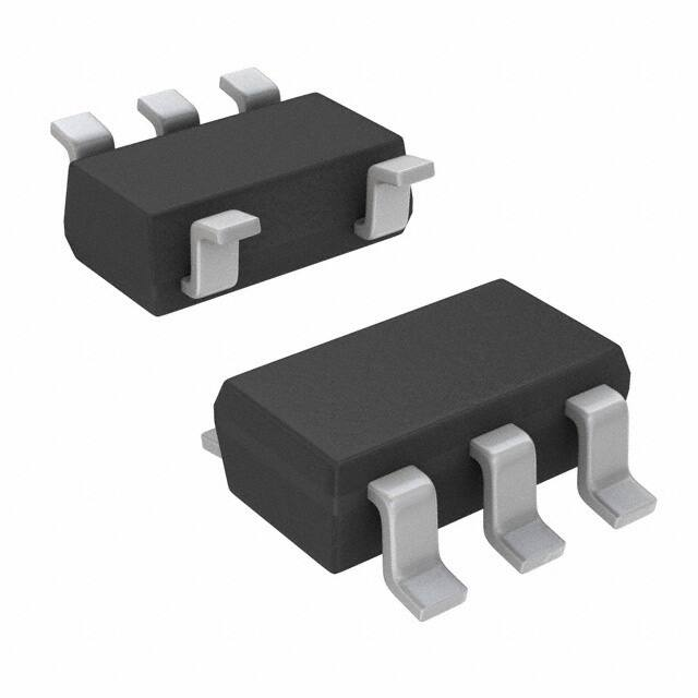
Package Type
5-Pin SOT-23
VSS 2
AIN 3
2002-2017 Microchip Technology Inc.
5
SCL
MCP3221
VDD 1
4 SDA
DS20001732E-page 1
�MCP3221
Functional Block Diagram
VDD
VSS
DAC
AIN
–
Sample
and
Hold
Comparator
+
12-bit SAR
Clock
Control Logic
I2C Interface
SCL
DS20001732E-page 2
SDA
2002-2017 Microchip Technology Inc.
�MCP3221
1.0
ELECTRICAL CHARACTERISTICS
Absolute Maximum Ratings †
VDD...........................................................................................................................................................................+7.0V
Analog input pin w.r.t. VSS ..................................................................................................................-0.6V to VDD +0.6V
SDA and SCL pins w.r.t. VSS ...............................................................................................................-0.6V to VDD +1.0V
Storage Temperature ............................................................................................................................. -65°C to +150°C
Ambient Temperature with power applied ............................................................................................... -65°C to +125°C
Maximum Junction Temperature ........................................................................................................................... +150°C
ESD protection on all pins (HBM) .......................................................................................................................... ≥ 4 kV
† Notice: Stresses above those listed under “Absolute Maximum Ratings” may cause permanent damage to the
device. This is a stress rating only and functional operation of the device at those or any other conditions above those
indicated in the operational listings of this specification is not intended. Exposure to maximum rating conditions for
extended periods may affect device reliability.
DC ELECTRICAL SPECIFICATIONS
Electrical Characteristics: Unless otherwise noted, all parameters apply at VDD = 5.0V, VSS = GND, RPU = 2 k
TA = -40°C to +85°C, I2C Fast Mode Timing: fSCL = 400 kHz (Note 3).
Parameter
Sym.
Min.
Typ.
Max.
Units
Conditions
DC Accuracy
Resolution
—
12
bits
Integral Nonlinearity
INL
—
±0.75
±2
LSB
Differential Nonlinearity
DNL
—
±0.5
±1
LSB
No missing codes
Offset Error
—
—
±0.75
±2
LSB
Gain Error
—
—
-1
±3
LSB
THD
—
-82
—
dB
VIN = 0.1V to 4.9V @ 1 kHz
Signal-to-Noise and Distortion
SINAD
—
72
—
dB
VIN = 0.1V to 4.9V @ 1 kHz
Spurious Free Dynamic Range
SFDR
—
86
—
dB
VIN = 0.1V to 4.9V @ 1 kHz
Input Voltage Range
—
VSS-0.3
—
VDD+0.3
V
2.7V VDD 5.5V
Leakage Current
—
-1
—
+1
µA
Dynamic Performance
Total Harmonic Distortion
Analog Input
SDA/SCL (open-drain output)
Data Coding Format
—
High-Level Input Voltage
VIH
0.7 VDD
—
—
Low-Level Input Voltage
VIL
—
—
0.3 VDD
V
Low-Level Output Voltage
VOL
—
—
0.4
V
Hysteresis of Schmitt Trigger Inputs
Straight Binary
—
V
IOL = 3 mA, RPU = 1.53 k
VHYST
—
0.05 VDD
—
V
fSCL = 400 kHz only
Input Leakage Current
ILI
-1
—
+1
µA
VIN = 0.1 VDD and 0.9 VDD
Output Leakage Current
ILO
-1
—
+1
µA
VOUT = 0.1 VSS and
0.9 VDD
Note 1:
2:
3:
4:
5:
Sample time is the time between conversions once the address byte has been sent to the converter. Refer
to Figure 5-6.
This parameter is periodically sampled and not 100% tested.
RPU = Pull-up resistor on SDA and SCL.
SDA and SCL = VSS to VDD at 400 kHz.
tACQ and tCONV are dependent on internal oscillator timing. See Figure 5-5 and Figure 5-6 in relation to
SCL.
2002-2017 Microchip Technology Inc.
DS20001732E-page 3
�MCP3221
DC ELECTRICAL SPECIFICATIONS (CONTINUED)
Electrical Characteristics: Unless otherwise noted, all parameters apply at VDD = 5.0V, VSS = GND, RPU = 2 k
TA = -40°C to +85°C, I2C Fast Mode Timing: fSCL = 400 kHz (Note 3).
Parameter
Sym.
Min.
Typ.
Max.
Units
CIN,
COUT
—
—
10
pF
TA = 25°C, f = 1 MHz;
(Note 2)
CB
—
—
400
pF
SDA drive low, 0.4V
Operating Voltage
VDD
2.7
—
5.5
V
Conversion Current
IDD
—
175
250
µA
Standby Current
IDDS
—
0.005
1
µA
SDA, SCL = VDD
Active Bus Current
IDDA
—
—
120
µA
Note 4
tCONV
—
8.96
—
µs
Note 5
Analog Input Acquisition Time
tACQ
—
1.12
—
µs
Note 5
Sample Rate
fSAMP
—
—
22.3
ksps
Pin Capacitance
(all inputs/outputs)
Bus Capacitance
Conditions
Power Requirements
Conversion Rate
Conversion Time
Note 1:
2:
3:
4:
5:
fSCL = 400 kHz (Note 1)
Sample time is the time between conversions once the address byte has been sent to the converter. Refer
to Figure 5-6.
This parameter is periodically sampled and not 100% tested.
RPU = Pull-up resistor on SDA and SCL.
SDA and SCL = VSS to VDD at 400 kHz.
tACQ and tCONV are dependent on internal oscillator timing. See Figure 5-5 and Figure 5-6 in relation to
SCL.
TEMPERATURE SPECIFICATIONS
Electrical Characteristics: Unless otherwise noted, all parameters apply at VDD = 5.0V, VSS = GND.
Parameter
Sym.
Min.
Typ.
Max.
Units
TA
-40
—
+125
°C
Extended Temperature Range
TA
-40
—
+125
°C
Storage Temperature Range
TA
-65
—
+150
°C
JA
—
256
—
°C/W
Conditions
Temperature Ranges
Operating Temperature Range
Thermal Package Resistances
Thermal Resistance, SOT-23
DS20001732E-page 4
2002-2017 Microchip Technology Inc.
�MCP3221
TIMING SPECIFICATIONS
Electrical Characteristics: All parameters apply at VDD = 2.7V - 5.5V, VSS = GND, TA = -40°C to +85°C.
Parameter
Sym.
Min.
Typ.
Max.
Units
Conditions
Clock Frequency
fSCL
0
—
100
kHz
Clock High Time
THIGH
4000
—
—
ns
Clock Low Time
TLOW
4700
—
—
ns
TR
—
—
1000
ns
From VIL to VIH (Note 1)
From VIL to VIH (Note 1)
I2C Standard Mode
SDA and SCL Rise Time
SDA and SCL Fall Time
TF
—
—
300
ns
Start Condition Hold Time
THD:STA
4000
—
—
ns
Start Condition Setup Time
TSU:STA
4700
—
—
ns
Data Input Setup Time
TSU:DAT
250
—
—
ns
Stop Condition Setup Time
TSU:STO
4000
—
—
ns
Stop Condition Hold time
THD:STD
4000
—
—
ns
Output Valid from Clock
TAA
—
—
3500
ns
Bus Free Time
TBUF
4700
—
—
ns
Note 2
Input Filter Spike Suppression
TSP
—
—
50
ns
SDA and SCL pins (Note 1)
Clock Frequency
FSCL
0
—
400
kHz
Clock High Time
THIGH
600
—
—
ns
Clock Low Time
2
I C Fast Mode
TLOW
1300
—
—
ns
SDA and SCL Rise Time
TR
20 + 0.1CB
—
300
ns
From VIL to VIH (Note 1)
SDA and SCL Fall Time
TF
20 + 0.1CB
—
300
ns
From VIL to VIH (Note 1)
Start Condition Hold Time
THD:STA
600
—
—
ns
Start Condition Setup Time
TSU:STA
600
—
—
ns
Data Input Hold Time
THD:DAT
0
—
0.9
ms
Data Input Setup Time
TSU:DAT
100
—
—
ns
Stop Condition Setup Time
TSU:STO
600
—
—
ns
Stop Condition Hold Time
THD:STD
600
—
—
ns
Output Valid from Clock
TAA
—
—
900
ns
Bus Free Time
TBUF
1300
—
—
ns
Note 2
Input Filter Spike Suppression
TSP
—
—
50
ns
SDA and SCL pins (Note 1)
Note 1:
2:
This parameter is periodically sampled and not 100% tested.
Time the bus must be free before a new transmission can start.
THIGH
TF
SCL
SDA
IN
TR
TSU:STA
TLOW
TSP
THD:DAT
TSU:DAT
TSU:STO
THD:STA
TAA
SDA
OUT
FIGURE 1-1:
VHYS
TBUF
Standard and Fast Mode Bus Timing Data.
2002-2017 Microchip Technology Inc.
DS20001732E-page 5
�MCP3221
2.0
TYPICAL PERFORMANCE CURVES
Note:
The graphs and tables provided following this note are a statistical summary based on a limited number of
samples and are provided for informational purposes only. The performance characteristics listed herein
are not tested or guaranteed. In some graphs or tables, the data presented may be outside the specified
operating range (e.g., outside specified power supply range) and therefore outside the warranted range.
1
0.8
0.6
0.4
0.2
0
-0.2
-0.4
-0.6
-0.8
-1
Negative INL
0
100
FIGURE 2-1:
INL (LSB)
INL (LSB)
Positive INL
200
300
I2C Bus Rate (kHz)
3.5
4
VDD (V)
4.5
5
200
300
400
INL vs. Clock Rate
1
0.8
0.6
0.4
0.2
0
-0.2
-0.4
-0.6
-0.8
-1
Positive INL
Negative INL
2.5
5.5
3
3.5
4
4.5
5
5.5
VDD (V)
FIGURE 2-2:
INL vs. VDD - I2C Standard
Mode (fSCL = 100 kHz).
FIGURE 2-5:
(fSCL = 400 kHz).
2
2
1.5
1.5
INL vs. VDD - I2C Fast Mode
1
INL (LSB)
1
INL (LSB)
100
FIGURE 2-4:
(VDD = 2.7V).
Negative INL
3
Negative INL
0
Positive INL
2.5
Positive INL
I2C Bus Rate (kHz)
INL vs. Clock Rate.
1
0.8
0.6
0.4
0.2
0
-0.2
-0.4
-0.6
-0.8
-1
1
0.8
0.6
0.4
0.2
0
-0.2
-0.4
-0.6
-0.8
-1
400
INL (LSB)
INL (LSB)
Note: Unless otherwise indicated, VDD = 5V, VSS = 0V, I2C Fast Mode Timing (SCL = 400 kHz), Continuous Conversion
Mode (fSAMP = 22.3 ksps), TA = +25°C.
0.5
0
-0.5
0.5
0
-0.5
-1
-1
-1.5
-1.5
-2
-2
0
1024
2048
Digital Code
FIGURE 2-3:
INL vs. Code
(Representative Part).
DS20001732E-page 6
3072
4096
0
1024
2048
3072
4096
Digital Code
FIGURE 2-6:
INL vs. Code
(Representative Part, VDD = 2.7V).
2002-2017 Microchip Technology Inc.
�MCP3221
1
0.8
0.6
0.4
0.2
0
-0.2
-0.4
-0.6
-0.8
-1
Positive INL
INL (LSB)
INL (LSB)
Note: Unless otherwise indicated, VDD = 5V, VSS = 0V, I2C Fast Mode Timing (SCL = 400 kHz), Continuous Conversion
Mode (fSAMP = 22.3 ksps), TA = +25°C.
Negative INL
-50
-25
0
25
50
75
100
1
0.8
0.6
0.4
0.2
0
-0.2
-0.4
-0.6
-0.8
-1
125
Positive INL
Negative INL
-50
-25
0
Temperature (°C)
INL vs. Temperature.
1
0.8
0.6
0.4
0.2
0
-0.2
-0.4
-0.6
-0.8
-1
FIGURE 2-10:
(VDD = 2.7V).
Positive DNL
DNL (LSB)
DNL (LSB)
FIGURE 2-7:
Negative DNL
0
100
200
300
1
0.8
0.6
0.4
0.2
0
-0.2
-0.4
-0.6
-0.8
-1
400
100
4
VDD (V)
DNL (LSB)
FIGURE 2-11:
(VDD = 2.7V).
DNL (LSB)
4.5
5
5.5
FIGURE 2-9:
DNL vs. VDD - I2C Standard
Mode (fSCL = 100 kHz).
2002-2017 Microchip Technology Inc.
200
300
400
I C Bus Rate (kHz)
Negative DNL
3.5
125
2
DNL vs. Clock Rate.
3
100
Negative DNL
0
Positive DNL
2.5
75
Positive DNL
2
1
0.8
0.6
0.4
0.2
0
-0.2
-0.4
-0.6
-0.8
-1
50
INL vs. Temperature
I C Bus Rate (kHz)
FIGURE 2-8:
25
Temperature (°C)
DNL vs. Clock Rate
1
0.8
0.6
0.4
0.2
0
-0.2
-0.4
-0.6
-0.8
-1
Positive DNL
Negative DNL
2.5
3
3.5
4
4.5
5
5.5
VDD (V)
FIGURE 2-12:
DNL vs. VDD - I2C Fast
Mode (fSCL = 400 kHz).
DS20001732E-page 7
�MCP3221
1
0.8
0.6
0.4
0.2
0
-0.2
-0.4
-0.6
-0.8
-1
DNL (LSB)
DNL (LSB)
Note: Unless otherwise indicated, VDD = 5V, VSS = 0V, I2C Fast Mode Timing (SCL = 400 kHz), Continuous Conversion
Mode (fSAMP = 22.3 ksps), TA = +25°C.
0
1024
2048
3072
1
0.8
0.6
0.4
0.2
0
-0.2
-0.4
-0.6
-0.8
-1
0
4096
1024
2048
FIGURE 2-16:
DNL vs. Code
(Representative Part, VDD = 2.7V).
Positive DNL
DNL (LSB)
DNL (LSB)
FIGURE 2-13:
DNL vs. Code
(Representative Part).
Negative DNL
-50
-25
0
25
50
75
100
125
1
0.8
0.6
0.4
0.2
0
-0.2
-0.4
-0.6
-0.8
-1
Positive DNL
Negative DNL
-50
-25
Temperature (°C)
0
-0.1
-0.2
-0.3
-0.4
-0.5
-0.6
-0.7
-0.8
-0.9
-1
DNL vs. Temperature.
Fast Mode
(fSCL= 100 kHz)
2.5
3
3.5
4.5
5
VDD (V)
FIGURE 2-15:
DS20001732E-page 8
FIGURE 2-17:
(VDD = 2.7V).
Standard Mode
(fSCL= 400 kHz)
4
0
25
50
75
100
125
Temperature (°C)
Offset Error (LSB)
Gain Error (LSB)
FIGURE 2-14:
4096
Digital Code
Digital Code
1
0.8
0.6
0.4
0.2
0
-0.2
-0.4
-0.6
-0.8
-1
3072
Gain Error vs. VDD.
5.5
DNL vs. Temperature
1
0.9
0.8
0.7
0.6
0.5
0.4
0.3
0.2
0.1
0
fSCL = 100 kHz & 400 kHz
2.5
3
FIGURE 2-18:
3.5
4
VDD (V)
4.5
5
5.5
Offset Error vs. VDD.
2002-2017 Microchip Technology Inc.
�MCP3221
Note: Unless otherwise indicated, VDD = 5V, VSS = 0V, I2C Fast Mode Timing (SCL = 400 kHz), Continuous Conversion
Mode (fSAMP = 22.3 ksps), TA = +25°C.
3
Offset Error (LSB)
Gain Error (LSB)
2
VDD = 2.7V
1
0
-1
-2
VDD = 5V
-3
-50
-25
0
25
50
75
100
2
1.8
1.6
1.4
1.2
1
0.8
0.6
0.4
0.2
0
VDD = 5V
VDD = 2.7V
-50
125
-25
0
Gain Error vs. Temperature.
100
90
80
70
60
50
40
30
20
10
0
FIGURE 2-22:
Temperature.
VDD = 5V
SINAD (dB)
SNR (dB)
FIGURE 2-19:
VDD = 2.7V
1
10
75
100
125
VDD = 5V
VDD = 2.7V
1
10
Input Frequency (kHz)
SNR vs. Input Frequency.
FIGURE 2-23:
SINAD vs. Input Frequency.
80
VDD = 5V
70
60
SINAD (dB)
THD (dB)
0
-10
-20
-30
-40
-50
-60
-70
-80
-90
-100
50
Offset Error vs.
100
90
80
70
60
50
40
30
20
10
0
Input Frequency (kHz)
FIGURE 2-20:
25
Temperature (°C)
Temperature (°C)
VDD = 5V
VDD = 2.7V
50
VDD = 2.7V
40
30
20
10
0
1
10
-40
Input Frequency (kHz)
FIGURE 2-21:
THD vs. Input Frequency.
2002-2017 Microchip Technology Inc.
-30
-20
-10
0
Input Signal Level (dB)
FIGURE 2-24:
Level.
SINAD vs. Input Signal
DS20001732E-page 9
�MCP3221
12
11.95
11.9
11.85
11.8
11.75
11.7
11.65
11.6
11.55
11.5
12
11.5
ENOB (rms)
VDD = 5V
10.5
10
9.5
9
2.5
3
3.5
FIGURE 2-25:
SFDR (dB)
VDD = 2.7V
11
100
90
80
70
60
50
40
30
20
10
0
4
VDD (V)
4.5
5
5.5
1
10
Input Frequency (kHz)
FIGURE 2-28:
ENOB vs. VDD.
fSAMP = 5.6 ksps
-10
VDD = 2.7V
-30
-50
-70
-90
-110
-130
1
0
10
500
FIGURE 2-26:
SFDR vs. Input Frequency.
250
-10
200
IDD (µA)
-30
-70
-90
1500
2000
2500
FIGURE 2-29:
Spectrum Using I2C
Standard Mode (Representative Part, 1 kHz
Input Frequency).
10
-50
1000
Frequency (Hz)
Input Frequency (kHz)
Amplitude (dB)
ENOB vs. Input Frequency.
10
VDD = 5V
Amplitude (dB)
ENOB (rms)
Note: Unless otherwise indicated, VDD = 5V, VSS = 0V, I2C Fast Mode Timing (SCL = 400 kHz), Continuous Conversion
Mode (fSAMP = 22.3 ksps), TA = +25°C.
150
100
50
-110
0
-130
0
2000
4000
6000
8000
10000
2.5
3
FIGURE 2-27:
Spectrum Using I2C Fast
Mode (Representative Part, 1 kHz Input
Frequency).
DS20001732E-page 10
3.5
4
4.5
5
5.5
VDD (V)
Frequency (Hz)
FIGURE 2-30:
IDD (Conversion) vs. VDD.
2002-2017 Microchip Technology Inc.
�MCP3221
200
180
160
140
120
100
80
60
40
20
0
100
90
80
70
60
50
40
30
20
10
0
IDDA (µA)
IDD (µA)
Note: Unless otherwise indicated, VDD = 5V, VSS = 0V, I2C Fast Mode Timing (SCL = 400 kHz), Continuous Conversion
Mode (fSAMP = 22.3 ksps), TA = +25°C.
VDD = 5V
VDD = 2.7V
0
100
200
300
2
I C Clock Rate (kHz)
FIGURE 2-31:
Rate.
0
IDDA (µA)
IDD (µA)
VDD = 5V
150
VDD = 2.7V
50
0
-50
-25
0
25
50
75
100
100
125
VDD = 5V
VDD = 2.7V
-50
-25
0
25
50
75
100
125
Temperature (°C)
IDD (Conversion) vs.
FIGURE 2-35:
Temperature.
100
90
80
70
60
50
40
30
20
10
0
IDDA (Active Bus) vs.
60
50
IDDS (pA)
IDDA (µA)
400
IDDA (Active Bus) vs. Clock
100
90
80
70
60
50
40
30
20
10
0
Temperature (°C)
FIGURE 2-32:
Temperature.
200
300
2
I C Clock Rate (kHz)
FIGURE 2-34:
Rate.
250
100
VDD = 2.7V
400
IDD (Conversion) vs. Clock
200
VDD = 5V
40
30
20
10
0
2.5
3
3.5
4
4.5
5
5.5
2.5
3
VDD (V)
FIGURE 2-33:
IDDA (Active Bus) vs. VDD.
2002-2017 Microchip Technology Inc.
3.5
4
4.5
5
5.5
VDD (V)
FIGURE 2-36:
IDDS (Standby) vs. VDD.
DS20001732E-page 11
�MCP3221
Note: Unless otherwise indicated, VDD = 5V, VSS = 0V, I2C Fast Mode Timing (SCL = 400 kHz), Continuous Conversion
Mode (fSAMP = 22.3 ksps), TA = +25°C.
2.1
Test Circuits
1000
100
VDD = 5V
IDDS (nA)
10
1
0.1
10 µF
0.01
2 k
0.001
0.0001
-50
-25
0
25
50
75
100
Analog Input Leakage (nA)
FIGURE 2-37:
Temperature.
AIN
125
Temperature (°C)
VIN
VDDSDA
MCP3221
VSS SCL
VCM = 2.5V
FIGURE 2-39:
-25
2 k
IDDS (Standby) vs.
2
1.8
1.6
1.4
1.2
1
0.8
0.6
0.4
0.2
0
-50
0.1 µF
0
25
50
75
100
Typical Test Configuration.
125
Temperature (°C)
FIGURE 2-38:
Temperature.
DS20001732E-page 12
Analog Input Leakage vs.
2002-2017 Microchip Technology Inc.
�MCP3221
3.0
PIN FUNCTIONS
Table 3-1 lists the function of the pins.
TABLE 3-1:
PIN FUNCTION TABLE
Name
3.1
Function
VDD
+2.7V to 5.5V Power Supply
VSS
Ground
AIN
Analog Input
SDA
Serial Data In/Out
SCL
Serial Clock In
VDD and VSS
The VDD pin, with respect to VSS, provides power to the
device as well as a voltage reference for the conversion
process. Refer to Section 6.4 “Device Power and
Layout Considerations” for tips on power and
grounding.
3.2
Analog Input (AIN)
AIN is the input pin to the sample and hold circuitry of
the Successive Approximation Register (SAR) converter. Care should be taken in driving this pin. Refer to
Section 6.1 “Driving the Analog Input” for more
information. For proper conversions, the voltage on this
pin can vary from VSS to VDD.
2002-2017 Microchip Technology Inc.
3.3
Serial Data (SDA)
SDA is a bidirectional pin used to transfer addresses
and data into and out of the device. It is an open-drain
terminal, therefore, the SDA bus requires a pull-up
resistor to VDD (typically 10 k for 100 kHz and 2 k
for 400 kHz SCL clock speeds). Refer to Section 6.2
“Connecting to the I2C Bus” for more information.
For normal data transfer, SDA is allowed to change only
during SCL low. Changes during SCL high are reserved
for indicating the Start and Stop conditions. Refer to
Section 5.1 “I2C Bus Characteristics” for more information.
3.4
Serial Clock (SCL)
SCL is an input pin used to synchronize the data transfer to and from the device on the SDA pin and is an
open-drain terminal. Therefore, the SCL bus requires a
pull-up resistor to VDD (typically 10 k for 100 kHz and
2 k for 400 kHz SCL clock speeds. Refer to
Section 6.2 “Connecting to the I2C Bus” for more
information.
For normal data transfer, SDA is allowed to change
only during SCL low. Changes during SCL high are
reserved for indicating the Start and Stop conditions.
Refer to Section 6.1 “Driving the Analog Input” for
more information.
DS20001732E-page 13
�MCP3221
4.0
DEVICE OPERATION
4.2
The MCP3221 employs a classic SAR architecture.
This architecture uses an internal sample and hold
capacitor to store the analog input while the conversion
is taking place. At the end of the acquisition time, the
input switch of the converter opens and the device uses
the collected charge on the internal sample and hold
capacitor to produce a serial 12-bit digital output code.
The acquisition time and conversion is self-timed using
an internal clock. After each conversion, the results are
stored in a 12-bit register that can be read at any time.
Communication with the device is accomplished with a
2-wire, I2C interface. Maximum sample rates of
22.3 ksps are possible with the MCP3221 in a continuous-conversion mode and an SCL clock rate of
400 kHz.
4.1
Digital Output Code
The digital output code produced by the MCP3221 is a
function of the input signal and power supply voltage,
VDD. As the VDD level is reduced, the LSB size is
reduced accordingly. The theoretical LSB size is shown
below.
EQUATION
V DD
LSB SIZE = -----------4096
VDD = Supply voltage
The output code of the MCP3221 is transmitted serially
with MSB first. The format of the code is straight binary.
Conversion Time (tCONV)
The conversion time is the time required to obtain the
digital result once the analog input is disconnected
from the holding capacitor. With the MCP3221, the
specified conversion time is typically 8.96 µs. This time
is dependent on the internal oscillator and is
independent of SCL.
4.3
Acquisition Time (tACQ)
The acquisition time is the amount of time the sample
cap array is acquiring charge.
The acquisition time is, typically, 1.12 µs. This time is
dependent on the internal oscillator and independent of
SCL.
4.4
Sample Rate
Sample rate is the inverse of the maximum amount of
time that is required from the point of acquisition of the
first conversion to the point of acquisition of the second
conversion.
The sample rate can be measured either by single or
continuous conversions. A single conversion includes
a Start bit, Address byte, two data bytes and a Stop bit.
This sample rate is measured from one Start bit to the
next Start bit.
For continuous conversions (requested by the Master
by issuing an Acknowledge after a conversion), the
maximum sample rate is measured from conversion to
conversion or a total of 18 clocks (two data bytes and
two Acknowledge bits). Refer to Section 5.2 “Device
Addressing” for more information.
Output Code
1111 1111 1111
1111 1111 1110
(4095)
(4094)
0000 0000 0011 (3)
0000 0000 0010 (2)
0000 0000 0001 (1)
0000 0000 0000 (0)
.5 LSB
1.5 LSB
2.5 LSB
FIGURE 4-1:
DS20001732E-page 14
AIN
VDD-1.5 LSB
VDD-2.5 LSB
Transfer Function.
2002-2017 Microchip Technology Inc.
�MCP3221
4.5
Differential Non-Linearity (DNL)
In the ideal A/D converter transfer function, each code
has a uniform width. That is, the difference in analog
input voltage is constant from one code transition point
to the next. Differential nonlinearity (DNL) specifies the
deviation of any code in the transfer function from an
ideal code width of 1 LSB. The DNL is determined by
subtracting the locations of successive code transition
points after compensating for any gain and offset
errors. A positive DNL implies that a code is longer than
the ideal code width, whereas a negative DNL implies
that a code is shorter than the ideal width.
4.6
Integral Non-Linearity (INL)
Integral nonlinearity (INL) is a result of cumulative DNL
errors and specifies how much the overall transfer
function deviates from a linear response. The method
of measurement used in the MCP3221 A/D converter
to determine INL is the end-point method.
4.7
Offset Error
Offset error is defined as a deviation of the code transition points that are present across all output codes.
This has the effect of shifting the entire A/D transfer
function. The offset error is measured by finding the difference between the actual location of the first code
transition and the desired location of the first transition.
The ideal location of the first code transition is located
at 1/2 LSB above VSS.
4.8
Gain Error
Gain error determines the amount of deviation from the
ideal slope of the A/D converter transfer function.
Before the gain error is determined, the offset error is
measured and subtracted from the conversion result.
The gain error can then be determined by finding the
location of the last code transition and comparing that
location to the ideal location. The ideal location of the
last code transition is 1.5 LSBs below full-scale or VDD.
4.9
Conversion Current (IDD)
Conversion current is the average amount of current
over the time required to perform a 12-bit conversion.
4.10
Active Bus Current (IDDA)
The average amount of current over the time required
to monitor the I2C bus. Any current that the device consumes while it is not being addressed is referred to as
Active Bus current.
4.11
Standby Current (IDDS)
The average amount of current required while no conversion is occurring and no data is being output (i.e.,
SCL and SDA lines are quiet).
4.12
I2C Standard Mode Timing
I2C specification where the frequency of SCL is
100 kHz.
4.13
I2C Fast Mode Timing
I2C specification where the frequency of SCL is
400 kHz.
2002-2017 Microchip Technology Inc.
DS20001732E-page 15
�MCP3221
5.0
SERIAL COMMUNICATIONS
5.1
I2C Bus Characteristics
The following bus protocol are defined:
• Data transfer may be initiated only when the bus
is not busy.
• During data transfer, the data line must remain
stable whenever the clock line is high. Changes in
the data line while the clock line is high will be
interpreted as a Start or Stop condition.
Accordingly, the following bus conditions are defined
(refer to Figure 5-1).
5.1.1
BUS NOT BUSY (A)
Both data and clock lines remain high.
5.1.2
START DATA TRANSFER (B)
A high-to-low transition of the SDA line while the clock
(SCL) is high determines a Start condition. All
commands must be preceded by a Start condition.
5.1.3
STOP DATA TRANSFER (C)
A low-to-high transition of the SDA line while the clock
(SCL) is high determines a Stop condition. All
operations must be ended with a Stop condition.
5.1.4
DATA VALID (D)
The state of the data line represents valid data when
after a START condition, the data line is stable for the
duration of the high period of the clock signal.
Each data transfer is initiated with a Start condition and
terminated with a Stop condition. The number of data
bytes being transferred between the Start and Stop
conditions is determined by the master device and is
unlimited.
5.1.5
ACKNOWLEDGE
Each receiving device, when addressed, is obliged to
generate an Acknowledge bit after the reception of
each byte. The master device must generate an extra
clock pulse that is associated with this Acknowledge
bit.
The device that acknowledges has to pull down the
SDA line during the acknowledge clock pulse in such a
way that the SDA line is stable low during the high
period of the acknowledge-related clock pulse. Setup
and hold times must be taken into account. During
reads, a master device must signal an end of data to
the slave by not generating an Acknowledge bit on the
last byte that is clocked out of the slave (NAK). In this
case, the slave (MCP3221) releases the bus to allow
the master device to generate the Stop condition.
The MCP3221 supports a bidirectional, 2-wire bus and
data transmission protocol. The device that sends data
onto the bus is the transmitter and the device receiving
data is the receiver. The bus has to be controlled by a
master device that generates the serial clock (SCL),
controls the bus access and generates the Start and
Stop conditions, whereas the MCP3221 works as a
slave device. Both master and slave devices can operate as either transmitter or receiver, but the master
device determines which mode is activated.
The data on the line must be changed during the low
period of the clock signal. There is one clock pulse per
bit of data.
SCL
(A)
(B)
(D)
(D)
(C)
(A)
SDA
START
CONDITION
FIGURE 5-1:
DS20001732E-page 16
DATA
ADDRESS OR
ACKNOWLEDGE ALLOWED
TO CHANGE
VALID
STOP
CONDITION
Data Transfer Sequence on the Serial Bus.
2002-2017 Microchip Technology Inc.
�MCP3221
Device Addressing
5.3
The address byte is the first byte received following the
Start condition from the master device. The first part of
the control byte consists of a 4-bit device code, which
is set to 1001 for the MCP3221. The device code is followed by three address bits: A2, A1 and A0. The default
address bits are 101. Contact the Microchip factory for
additional address bit options. The address bits allow
up to eight MCP3221 devices on the same bus and are
used to determine which device is accessed.
The eighth bit of the slave address determines if the
master device wants to read conversion data or write to
the MCP3221. When set to a 1, a read operation is
selected. When set to a 0, a write operation is selected.
There are no writable registers on the MCP3221, therefore, this bit must be set to a 1 to initiate a conversion.
The MCP3221 is a slave device that is compatible with
the 2-wire I2C serial interface protocol. A hardware
connection diagram is shown in Figure 6-2. Communication is initiated by the microcontroller (master
device), which sends a Start bit followed by the address
byte.
On completion of the conversion(s) performed by the
MCP3221, the microcontroller must send a Stop bit to
end the communication.
The last bit in the device address byte is the R/W bit.
When this bit is a logic 1, a conversion is executed. Setting this bit to logic 0 also results in an Acknowledge
(ACK) from the MCP3221, with the device then releasing the bus. This can be used for device polling. Refer
to Section 6.3 “Device Polling” for more information.
START
Executing a Conversion
This section describes the details of communicating
with the MCP3221 device. Initiating the sample and
hold acquisition, reading the conversion data, and
executing multiple conversions are discussed.
5.3.1
INITIATING THE SAMPLE AND
HOLD
The acquisition and conversion of the input signal
begins with the falling edge of the R/W bit of the
address byte. At this point, the internal clock initiates
the sample, hold and conversion cycle, all of which are
internal to the ADC.
tACQ + tCONV is
initiated here
Address Byte
SCL
1
2
3
4
SDA
1
0
0
1 A2 A1 A0 R/W
Start
bit
FIGURE 5-3:
Address Byte.
READ/WRITE
6
7
8
9
Address bits
Initiating the Conversion,
tACQ + tCONV is
initiated here
R/W A
SLAVE ADDRESS
Device bits
5
ACK
5.2
Lower Data Byte (n)
17 18 19 20 21 22 23 24 25 26
SCL
0
Device code
1
1
0
1
Address bits(1)
Note 1: Contact Microchip for additional address bits.
FIGURE 5-2:
Device Addressing.
2002-2017 Microchip Technology Inc.
SDA
D8
D7 D6 D5 D4 D3 D2 D2 D0
ACK
0
ACK
1
FIGURE 5-4:
Initiating the Conversion,
Continuous Conversions.
DS20001732E-page 17
�MCP3221
5.3.2
The input signal is initially sampled with the first falling
edge of the clock following the transmission of a
logic-high R/W bit. Additionally, with the rising edge of
the SCL, the ADC transmits an Acknowledge bit (ACK
= 0). The master must release the data bus during this
clock pulse to allow the MCP3221 to pull the line low
(refer to Figure 5-3).
READING THE CONVERSION DATA
After the MCP3221 acknowledges the address byte, the
device transmits four 0 bits followed by the upper four
data bits of the conversion. The master device acknowledges this byte with an ACK = Low. With the following
eight clock pulses, the MCP3221 transmits the lower
eight data bits from the conversion. The master sends
an ACK = high, indicating to the MCP3221 that no more
data is requested. The master can send a Stop bit to
end the transmission.
For consecutive samples, sampling begins on the falling edge of the LSB of the conversion result, which is
two bytes long. Refer to Figure 5-6 for the timing
diagram.
tACQ + tCONV is
initiated here
1
2
3
4
5
6
7
8
9
10 11 12 13 14 15 16 17 18 19 20 21 22 23 24 25 26 27
SCL
S
T
A
R
T
1
S
SDA
0
0
FIGURE 5-5:
A
2
1
Device bits
5.3.3
Upper Data Byte
Address Byte
A
1
A
C
K
R
/
W
A
0
0
0
0
0
D D D
11 10 9
S
T
O
P
Lower Data Byte
A
C D
K 7
D
8
D
6
D
5
D
4
D
3
D
2
D
1
N
A
K
D
0
P
Address bits
Executing a Conversion.
CONSECUTIVE CONVERSIONS
For consecutive samples, sampling begins on the falling edge of the LSB of the conversion result. See
Figure 5-6 for timing.
tACQ + tCONV is
initiated here
tACQ + tCONV is
initiated here
fSAMP = 22.3 ksps (fCLK = 400 kHz)
1
2
3
4
5
6
7
8
9
10 11 12 13 14 15 16 17 18 19 20 21 22 23 24 25 26 27 28
SCL
S
T
A
R
T
SDA
S
Upper Data Byte (n)
Address Byte
1
0
0
Device bits
FIGURE 5-6:
DS20001732E-page 18
1 A2 A1 A0
R
/
W
A
C
K
0
0
0
0
D D D
11 10 9
Lower Data Byte (n)
D
8
A
C
K
D
7
D
6
D
5
D
4
D
3
D
2
D
1
D
0
A
C
K
0
Address bits
Continuous Conversion.
2002-2017 Microchip Technology Inc.
�MCP3221
6.0
APPLICATIONS INFORMATION
6.1
Driving the Analog Input
The MCP3221 has a single-ended analog input (AIN).
For proper conversion results, the voltage at the AIN pin
must be kept between VSS and VDD. If the converter
has no offset error, gain error, INL or DNL errors, and
the voltage level of AIN is equal to or less than
VSS + 1/2 LSB, the resultant code is 000h. Additionally, if the voltage at AIN is equal to or greater than
VDD - 1.5 LSB, the output code is FFFh.
The analog input model is shown in Figure 6-1. In this
diagram, the source impedance (RSS) adds to the internal sampling switch (RS) impedance, directly affecting
the time required to charge the capacitor (CSAMPLE).
Consequently, a larger source impedance increases
the offset error, gain error and integral linearity errors of
the conversion. Ideally, the impedance of the signal
source should be near zero. This is achievable with an
operational amplifier such as the MCP6022, which has
a closed-loop output impedance of tens of ohms.
VDD
RSS
Sampling
Switch
VT = 0.6V
AIN
CPIN
7 pF
VA
VT = 0.6V
SS
RS = 1 k
CSAMPLE
= DAC capacitance
= 20 pF
ILEAKAGE
±1 nA
VSS
Legend
VA
RSS
AIN
CPIN
VT
ILEAKAGE
SS
RS
CSAMPLE
=
=
=
=
=
=
=
=
=
FIGURE 6-1:
6.2
signal source
source impedance
analog input pad
analog input pin capacitance
threshold voltage
leakage current at the pin
due to various junctions
sampling switch
sampling switch resistor
sample/hold capacitance
Analog Input Model, AIN.
Connecting to the I2C Bus
The I2C bus is an open collector bus, requiring pull-up
resistors connected to the SDA and SCL lines. This
configuration is shown in Figure 6-2.
The number of devices connected to the bus is only
limited by the maximum bus capacitance of 400 pF. A
possible configuration using multiple devices is shown
in Figure 6-3.
SDA SCL
VDD
PIC®
Microcontroller
PIC16F876
Microcontroller
RPU
RPU MCP3221
SDA
AIN
SCL
24LC01
EEPROM
Analog
Input
Signal
MCP3221
12-bit ADC
TC74
Temperature
Sensor
RPU is typically: 10 k for fSCL = 100 kHz
2 k for fSCL = 400 kHz
FIGURE 6-2:
Bus.
Pull-up Resistors on I2C
2002-2017 Microchip Technology Inc.
FIGURE 6-3:
Multiple Devices on I2C Bus.
DS20001732E-page 19
�MCP3221
6.3
Device Polling
6.4.2
In some instances, it may be necessary to test for
MCP3221 presence on the I2C bus without performing
a conversion as described in Figure 6-4 where the R/W
bit in the address byte is set to a zero. The MCP3221
acknowledges by pulling SDA low during the ACK clock
and then release the bus back to the I2C master. A Stop
or repeated Start bit can be issued from the master and
I2C communication can continue.
Address Byte
1 0 0
SDA
1
ACK
1 2 3 4 5 6 7 8 9
SCL
A2 A1A0 0
Start
R/W
bit Device bits Address bits
Start
bit
MCP3221 response
FIGURE 6-4:
6.4
6.4.1
Device Polling.
Device Power and Layout
Considerations
LAYOUT CONSIDERATIONS
When laying out a printed circuit board for use with
analog components, care should be taken to reduce
noise wherever possible. A bypass capacitor from VDD
to ground must be used always with this device and
placed as close as possible to the device pin. A bypass
capacitor value of 0.1 µF is recommended.
Digital and analog traces should be separated as much
as possible on the board, with no traces running
underneath the device or the bypass capacitor. Extra
precautions should be taken to keep traces with highfrequency signals (such as clock lines) as far as
possible from analog traces.
Use of an analog ground plane is recommended in
order to keep the ground potential the same for all
devices on the board. Providing VDD connections to
devices in a Star configuration can also reduce noise
by eliminating current return paths and associated
errors (Figure 6-6). For more information on layout tips
when using the MCP3221 or other ADC devices, refer
to the Microchip Technology Application Note, “AN688
Layout Tips for 12-Bit A/D Converter Application”
(DS00688).
VDD
Connection
POWERING THE MCP3221
VDD supplies the power to the device and the reference
voltage. A bypass capacitor value of 0.1 µF is recommended. Adding a 10 µF capacitor in parallel is recommended to attenuate higher frequency noise that is
present in some systems.
Device 4
Device 1
VDD
Device 3
VDD
10 µF
Device 2
0.1 µF
VDD
AIN
MCP3221
FIGURE 6-5:
Note:
SCL
SDA
RPU RPU
To
Microcontroller
FIGURE 6-6:
VDD traces arranged in a
Star configuration in order to reduce errors
caused by current return paths.
Powering the MCP3221.
When power-down of the MCP3221 is
needed during applications (after powerup), it is highly recommended to bring
down the VDD to VSS level. This can guarantee a Full Reset of the device for the
next power-up cycle.
DS20001732E-page 20
2002-2017 Microchip Technology Inc.
�MCP3221
6.4.3
USING A REFERENCE FOR
SUPPLY
The MCP3221 uses VDD as power and also as a reference. In some applications, it may be necessary to use
a stable reference to achieve the required accuracy.
Figure 6-7 shows an example using the MCP1541 as a
4.096V, 2% reference.
VDD
1 µF
MCP1541
CL
4.096V
Reference
AIN
VDD
SCL
MCP3221
SDA
RPU
To
Microcontroller
0.1 µF
VDD
FIGURE 6-7:
Stable Power and
Reference Configuration.
2002-2017 Microchip Technology Inc.
DS20001732E-page 21
�MCP3221
7.0
PACKAGING INFORMATION
7.1
Package Marking Information
5-Pin SOT-23
3
2
1
4
Part Number
2
1
3
4
5
Address Option
SOT-23
MCP3221A0T-E/OT
000
GE
MCP3221A1T-E/OT
001
GH
MCP3221A2T-E/OT
010
GB
MCP3221A3T-E/OT
011
GC
MCP3221A4T-E/OT
100
GD
GA *
MCP3221A5T-E/OT
101
MCP3221A6T-E/OT
110
GF
MCP3221A7T-E/OT
111
GG
* Default option. Contact Microchip Factory for other
address options.
Legend: XX...X
Y
YY
WW
NNN
e3
*
Note:
DS20001732E-page 22
Customer-specific information
Year code (last digit of calendar year)
Year code (last 2 digits of calendar year)
Week code (week of January 1 is week ‘01’)
Alphanumeric traceability code
Pb-free JEDEC designator for Matte Tin (Sn)
This package is Pb-free. The Pb-free JEDEC designator ( e3 )
can be found on the outer packaging for this package.
In the event the full Microchip part number cannot be marked on one line, it will
be carried over to the next line, thus limiting the number of available
characters for customer-specific information.
2002-2017 Microchip Technology Inc.
�MCP3221
5-Lead Plastic Small Outline Transistor (OT) (SOT-23)
Note:
For the most current package drawings, please see the Microchip Packaging Specification located
at http://www.microchip.com/packaging
E
E1
p
B
p1
n
D
1
c
A
L
A1
INCHES*
Units
Dimension Limits
A2
MIN
MILLIMETERS
NOM
MAX
MIN
NOM
MAX
Pitch
n
p
.038
0.95
Outside lead pitch (basic)
p1
.075
1.90
Number of Pins
Overall Height
5
5
A
.035
.046
.057
0.90
1.18
1.45
Molded Package Thickness
A2
.035
.043
.051
0.90
1.10
1.30
Standoff
A1
.000
.003
.006
0.00
0.08
0.15
Overall Width
E
.102
.110
.118
2.60
2.80
3.00
Molded Package Width
E1
.059
.064
.069
1.50
1.63
1.75
Overall Length
D
.110
.116
.122
2.80
2.95
3.10
Foot Length
.014
.018
.022
0.35
0.45
Foot Angle
L
f
Lead Thickness
c
.004
Lead Width
B
a
.014
Mold Draft Angle Top
Mold Draft Angle Bottom
b
0
5
.006
.017
10
0
0.55
5
.008
0.09
0.15
.020
0.35
0.43
10
0.20
0.50
0
5
10
0
5
10
0
5
10
0
5
10
* Controlling Parameter
Notes:
Dimensions D and E1 do not include mold flash or protrusions. Mold flash or protrusions shall not exceed .005" (0.127mm) per side.
EIAJ Equivalent: SC-74A
Revised 09-12-05
Drawing No. C04-091
2002-2017 Microchip Technology Inc.
DS20001732E-page 23
�MCP3221
NOTES:
DS20001732E-page 24
2002-2017 Microchip Technology Inc.
�MCP3221
APPENDIX A:
REVISION HISTORY
Revision E (January 2017)
• Added a note to Section 6.4.1 “Powering the
MCP3221”.
• Fixed Section 7.1 “Package Marking Information” format to reflect the correct package marking as “1 2 3 4” instead of “1 10 10 10”.
• Updated Temperature Specifiations table to
remove information on Industrial Temperature
Range
Revision D (January 2013)
• Added a note to each package outline drawing.
Revision C (July 2006)
• Updated Section 5.2 “Device Addressing”:
changed 4-bit device code to “1001”. Changed
three address bits to “101”.
Revision B (May 2003)
• Numerous changes throughout document.
Revision A (November 2002)
• Original Release of this Document.
2002-2017 Microchip Technology Inc.
DS20001732E-page 25
�MCP3221
NOTES:
DS20001732E-page 26
2002-2017 Microchip Technology Inc.
�MCP3221
PRODUCT IDENTIFICATION SYSTEM
To order or obtain information, e.g., on pricing or delivery, refer to the factory or the listed sales office.
PART NO.
XX
X
/XX
Device
Address
Options
Temperature
Range
Package
Device:
Examples:
a)
b)
MCP3221T: 12-Bit 2-Wire Serial A/D Converter
(Tape and Reel)
c)
d)
Temperature Range:
Address Options:
E = -40C to +125C
XX
e)
A2
A1
A0
A0
=
0
0
0
A1
=
0
0
1
A2
=
0
1
0
A3
=
0
1
1
0
A4
=
1
0
A5 *
=
1
0
1
A6
=
1
1
0
A7
=
1
1
1
f)
g)
h)
MCP3221A0T-E/OT: Extended, A0 Address,
Tape and Reel
MCP3221A1T-E/OT: Extended, A1 Address,
Tape and Reel
MCP3221A2T-E/OT: Extended, A2 Address,
Tape and Reel
MCP3221A3T-E/OT: Extended, A3 Address,
Tape and Reel
MCP3221A4T-E/OT: Extended, A4 Address,
Tape and Reel
MCP3221A5T-E/OT: Extended, A5 Address,
Tape and Reel
MCP3221A6T-E/OT: Extended, A6 Address,
Tape and Reel
MCP3221A7T-IE/OT: Extended, A7 Address,
Tape and Reel
* Default option. Contact Microchip factory for other
address options
Package:
OT = SOT-23, 5-lead (Tape and Reel)
2002-2017 Microchip Technology Inc.
DS20001732E-page 27
�MCP3221
NOTES:
DS20001732E-page 28
2002-2017 Microchip Technology Inc.
�Note the following details of the code protection feature on Microchip devices:
•
Microchip products meet the specification contained in their particular Microchip Data Sheet.
•
Microchip believes that its family of products is one of the most secure families of its kind on the market today, when used in the
intended manner and under normal conditions.
•
There are dishonest and possibly illegal methods used to breach the code protection feature. All of these methods, to our
knowledge, require using the Microchip products in a manner outside the operating specifications contained in Microchip’s Data
Sheets. Most likely, the person doing so is engaged in theft of intellectual property.
•
Microchip is willing to work with the customer who is concerned about the integrity of their code.
•
Neither Microchip nor any other semiconductor manufacturer can guarantee the security of their code. Code protection does not
mean that we are guaranteeing the product as “unbreakable.”
Code protection is constantly evolving. We at Microchip are committed to continuously improving the code protection features of our
products. Attempts to break Microchip’s code protection feature may be a violation of the Digital Millennium Copyright Act. If such acts
allow unauthorized access to your software or other copyrighted work, you may have a right to sue for relief under that Act.
Information contained in this publication regarding device
applications and the like is provided only for your convenience
and may be superseded by updates. It is your responsibility to
ensure that your application meets with your specifications.
MICROCHIP MAKES NO REPRESENTATIONS OR
WARRANTIES OF ANY KIND WHETHER EXPRESS OR
IMPLIED, WRITTEN OR ORAL, STATUTORY OR
OTHERWISE, RELATED TO THE INFORMATION,
INCLUDING BUT NOT LIMITED TO ITS CONDITION,
QUALITY, PERFORMANCE, MERCHANTABILITY OR
FITNESS FOR PURPOSE. Microchip disclaims all liability
arising from this information and its use. Use of Microchip
devices in life support and/or safety applications is entirely at
the buyer’s risk, and the buyer agrees to defend, indemnify and
hold harmless Microchip from any and all damages, claims,
suits, or expenses resulting from such use. No licenses are
conveyed, implicitly or otherwise, under any Microchip
intellectual property rights unless otherwise stated.
Microchip received ISO/TS-16949:2009 certification for its worldwide
headquarters, design and wafer fabrication facilities in Chandler and
Tempe, Arizona; Gresham, Oregon and design centers in California
and India. The Company’s quality system processes and procedures
are for its PIC® MCUs and dsPIC® DSCs, KEELOQ® code hopping
devices, Serial EEPROMs, microperipherals, nonvolatile memory and
analog products. In addition, Microchip’s quality system for the design
and manufacture of development systems is ISO 9001:2000 certified.
QUALITY MANAGEMENT SYSTEM
CERTIFIED BY DNV
== ISO/TS 16949 ==
2002-2017 Microchip Technology Inc.
Trademarks
The Microchip name and logo, the Microchip logo, AnyRate, AVR,
AVR logo, AVR Freaks, BeaconThings, BitCloud, CryptoMemory,
CryptoRF, dsPIC, FlashFlex, flexPWR, Heldo, JukeBlox, KEELOQ,
KEELOQ logo, Kleer, LANCheck, LINK MD, maXStylus,
maXTouch, MediaLB, megaAVR, MOST, MOST logo, MPLAB,
OptoLyzer, PIC, picoPower, PICSTART, PIC32 logo, Prochip
Designer, QTouch, RightTouch, SAM-BA, SpyNIC, SST, SST
Logo, SuperFlash, tinyAVR, UNI/O, and XMEGA are registered
trademarks of Microchip Technology Incorporated in the U.S.A.
and other countries.
ClockWorks, The Embedded Control Solutions Company,
EtherSynch, Hyper Speed Control, HyperLight Load, IntelliMOS,
mTouch, Precision Edge, and Quiet-Wire are registered
trademarks of Microchip Technology Incorporated in the U.S.A.
Adjacent Key Suppression, AKS, Analog-for-the-Digital Age, Any
Capacitor, AnyIn, AnyOut, BodyCom, chipKIT, chipKIT logo,
CodeGuard, CryptoAuthentication, CryptoCompanion,
CryptoController, dsPICDEM, dsPICDEM.net, Dynamic Average
Matching, DAM, ECAN, EtherGREEN, In-Circuit Serial
Programming, ICSP, Inter-Chip Connectivity, JitterBlocker,
KleerNet, KleerNet logo, Mindi, MiWi, motorBench, MPASM, MPF,
MPLAB Certified logo, MPLIB, MPLINK, MultiTRAK, NetDetach,
Omniscient Code Generation, PICDEM, PICDEM.net, PICkit,
PICtail, PureSilicon, QMatrix, RightTouch logo, REAL ICE, Ripple
Blocker, SAM-ICE, Serial Quad I/O, SMART-I.S., SQI,
SuperSwitcher, SuperSwitcher II, Total Endurance, TSHARC,
USBCheck, VariSense, ViewSpan, WiperLock, Wireless DNA, and
ZENA are trademarks of Microchip Technology Incorporated in the
U.S.A. and other countries.
SQTP is a service mark of Microchip Technology Incorporated in
the U.S.A.
Silicon Storage Technology is a registered trademark of Microchip
Technology Inc. in other countries.
GestIC is a registered trademark of Microchip Technology
Germany II GmbH & Co. KG, a subsidiary of Microchip Technology
Inc., in other countries.
All other trademarks mentioned herein are property of their
respective companies.
© 2002-2017, Microchip Technology Incorporated, All Rights
Reserved.
ISBN: 978-1-5224-1291-5
DS20001732E-page 11
�Worldwide Sales and Service
AMERICAS
ASIA/PACIFIC
ASIA/PACIFIC
EUROPE
Corporate Office
2355 West Chandler Blvd.
Chandler, AZ 85224-6199
Tel: 480-792-7200
Fax: 480-792-7277
Technical Support:
http://www.microchip.com/
support
Web Address:
www.microchip.com
Asia Pacific Office
Suites 3707-14, 37th Floor
Tower 6, The Gateway
Harbour City, Kowloon
China - Xiamen
Tel: 86-592-2388138
Fax: 86-592-2388130
Austria - Wels
Tel: 43-7242-2244-39
Fax: 43-7242-2244-393
China - Zhuhai
Tel: 86-756-3210040
Fax: 86-756-3210049
Denmark - Copenhagen
Tel: 45-4450-2828
Fax: 45-4485-2829
India - Bangalore
Tel: 91-80-3090-4444
Fax: 91-80-3090-4123
Finland - Espoo
Tel: 358-9-4520-820
Atlanta
Duluth, GA
Tel: 678-957-9614
Fax: 678-957-1455
Hong Kong
Tel: 852-2943-5100
Fax: 852-2401-3431
Australia - Sydney
Tel: 61-2-9868-6733
Fax: 61-2-9868-6755
China - Beijing
Tel: 86-10-8569-7000
Fax: 86-10-8528-2104
Austin, TX
Tel: 512-257-3370
China - Chengdu
Tel: 86-28-8665-5511
Fax: 86-28-8665-7889
Boston
Westborough, MA
Tel: 774-760-0087
Fax: 774-760-0088
China - Chongqing
Tel: 86-23-8980-9588
Fax: 86-23-8980-9500
Chicago
Itasca, IL
Tel: 630-285-0071
Fax: 630-285-0075
Dallas
Addison, TX
Tel: 972-818-7423
Fax: 972-818-2924
Detroit
Novi, MI
Tel: 248-848-4000
Houston, TX
Tel: 281-894-5983
Indianapolis
Noblesville, IN
Tel: 317-773-8323
Fax: 317-773-5453
Tel: 317-536-2380
Los Angeles
Mission Viejo, CA
Tel: 949-462-9523
Fax: 949-462-9608
Tel: 951-273-7800
Raleigh, NC
Tel: 919-844-7510
New York, NY
Tel: 631-435-6000
San Jose, CA
Tel: 408-735-9110
Tel: 408-436-4270
Canada - Toronto
Tel: 905-695-1980
Fax: 905-695-2078
DS20001732E-page 30
China - Dongguan
Tel: 86-769-8702-9880
China - Guangzhou
Tel: 86-20-8755-8029
China - Hangzhou
Tel: 86-571-8792-8115
Fax: 86-571-8792-8116
China - Hong Kong SAR
Tel: 852-2943-5100
Fax: 852-2401-3431
China - Nanjing
Tel: 86-25-8473-2460
Fax: 86-25-8473-2470
China - Qingdao
Tel: 86-532-8502-7355
Fax: 86-532-8502-7205
China - Shanghai
Tel: 86-21-3326-8000
Fax: 86-21-3326-8021
China - Shenyang
Tel: 86-24-2334-2829
Fax: 86-24-2334-2393
China - Shenzhen
Tel: 86-755-8864-2200
Fax: 86-755-8203-1760
France - Paris
Tel: 33-1-69-53-63-20
Fax: 33-1-69-30-90-79
India - New Delhi
Tel: 91-11-4160-8631
Fax: 91-11-4160-8632
France - Saint Cloud
Tel: 33-1-30-60-70-00
India - Pune
Tel: 91-20-3019-1500
Germany - Garching
Tel: 49-8931-9700
Germany - Haan
Tel: 49-2129-3766400
Japan - Osaka
Tel: 81-6-6152-7160
Fax: 81-6-6152-9310
Japan - Tokyo
Tel: 81-3-6880- 3770
Fax: 81-3-6880-3771
Germany - Heilbronn
Tel: 49-7131-67-3636
Germany - Karlsruhe
Tel: 49-721-625370
Korea - Daegu
Tel: 82-53-744-4301
Fax: 82-53-744-4302
Germany - Munich
Tel: 49-89-627-144-0
Fax: 49-89-627-144-44
Korea - Seoul
Tel: 82-2-554-7200
Fax: 82-2-558-5932 or
82-2-558-5934
Germany - Rosenheim
Tel: 49-8031-354-560
Malaysia - Kuala Lumpur
Tel: 60-3-6201-9857
Fax: 60-3-6201-9859
Malaysia - Penang
Tel: 60-4-227-8870
Fax: 60-4-227-4068
Philippines - Manila
Tel: 63-2-634-9065
Fax: 63-2-634-9069
Singapore
Tel: 65-6334-8870
Fax: 65-6334-8850
Taiwan - Hsin Chu
Tel: 886-3-5778-366
Fax: 886-3-5770-955
Taiwan - Kaohsiung
Tel: 886-7-213-7830
China - Wuhan
Tel: 86-27-5980-5300
Fax: 86-27-5980-5118
Taiwan - Taipei
Tel: 886-2-2508-8600
Fax: 886-2-2508-0102
China - Xian
Tel: 86-29-8833-7252
Fax: 86-29-8833-7256
Thailand - Bangkok
Tel: 66-2-694-1351
Fax: 66-2-694-1350
Israel - Ra’anana
Tel: 972-9-744-7705
Italy - Milan
Tel: 39-0331-742611
Fax: 39-0331-466781
Italy - Padova
Tel: 39-049-7625286
Netherlands - Drunen
Tel: 31-416-690399
Fax: 31-416-690340
Norway - Trondheim
Tel: 47-7289-7561
Poland - Warsaw
Tel: 48-22-3325737
Romania - Bucharest
Tel: 40-21-407-87-50
Spain - Madrid
Tel: 34-91-708-08-90
Fax: 34-91-708-08-91
Sweden - Gothenberg
Tel: 46-31-704-60-40
Sweden - Stockholm
Tel: 46-8-5090-4654
UK - Wokingham
Tel: 44-118-921-5800
Fax: 44-118-921-5820
2002-2017 Microchip Technology Inc.
11/07/16
�


 工商网监
湘ICP备2023018690号
工商网监
湘ICP备2023018690号
