MCP6541/1R/1U/2/3/4
Push-Pull Output Sub-Microamp Comparators
Features
Description
•
•
•
•
The Microchip Technology Inc. MCP6541/1R/1U/2/3/4
family of comparators is offered in single (MCP6541,
MCP6541R, MCP6541U), single with Chip Select (CS)
(MCP6543), dual (MCP6542) and quad (MCP6544)
configurations. The outputs are push-pull (CMOS/TTLcompatible) and are capable of driving heavy DC or
capacitive loads.
•
•
•
•
•
•
•
Low Quiescent Current: 600 nA/Comparator (typ.)
Rail-to-Rail Input: VSS - 0.3V to VDD + 0.3V
CMOS/TTL-Compatible Output
Propagation Delay: 4 µs
(typical, 100 mV Overdrive)
Wide Supply Voltage Range: 1.6V to 5.5V
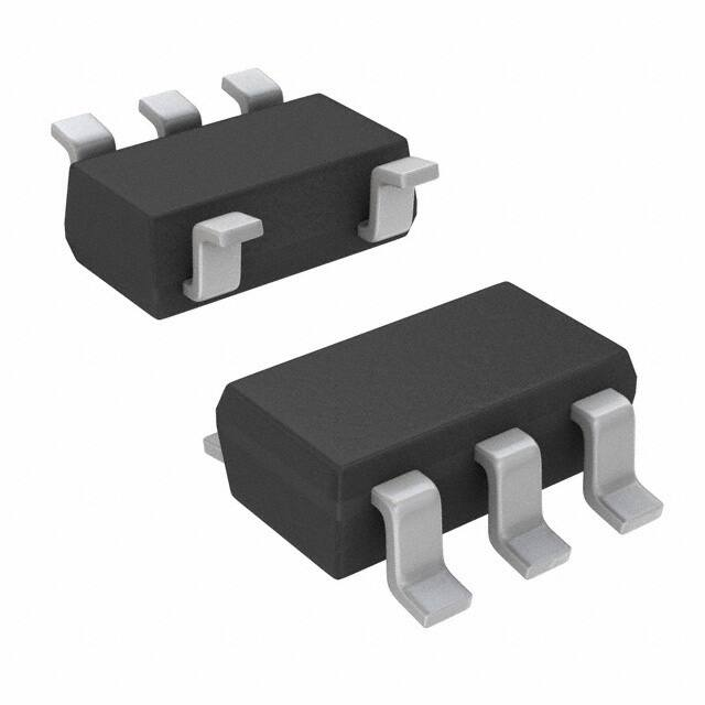
Available in Single, Dual and Quad
Single Available in SOT-23-5, SC-70-5 * Packages
Chip Select (CS) with MCP6543
Low Switching Current
Internal Hysteresis: 3.3 mV (typ.)
Temperature Ranges:
- Industrial: -40°C to +85°C
- Extended: -40°C to +125°C
Typical Applications
•
•
•
•
•
•
•
•
Laptop Computers
Mobile Phones
Metering Systems
Hand-held Electronics
RC Timers
Alarm and Monitoring Circuits
Windowed Comparators
Multivibrators
These comparators are optimized for low-power,
single-supply operation with greater than rail-to-rail
input operation. The push-pull output of the
MCP6541/1R/1U/2/3/4 family supports rail-to-rail output swing and interfaces with TTL/CMOS logic. The
internal input hysteresis eliminates output switching
due to internal input noise voltage, reducing current
draw. The output limits supply current surges and
dynamic power consumption while switching. This
product family operates with a single-supply voltage as
low as 1.6V and draws less than 1 µA/comparator of
quiescent current.
The related MCP6546/7/8/9 family of comparators from
Microchip has an open-drain output. Used with a pullup resistor, these devices can be used as level-shifters
for any desired voltage up to 10V and in wired-OR
logic.
* SC-70-5 E-Temp parts not available at this release of
the data sheet.
MCP6541U SOT-23-5 is E-Temp only.
Related Devices
• Open-Drain Output: MCP6546/7/8/9
Package Types
MCP6541
PDIP, SOIC, MSOP
7 VDD
OUT 1
VDD 2
6 OUT
VIN+ 3
MCP6541
SC-70-5, SOT-23-5
5 VDD
OUT 1
-
VIN+ 3
+
VSS 2
4 VIN–
4 VIN–
MCP6541U
SC-70-5, SOT-23-5
VIN+ 1
VSS 2
VIN– 3
2019-2020 Microchip Technology Inc.
MCP6542
PDIP, SOIC, MSOP
8 VDD
OUTA 1
VINA– 2
5 NC
+
VINA+ 3
VSS 4
+
5 VSS
+
VIN– 2
8 NC
-
NC 1
MCP6541R
SOT-23-5
-
+
-
6 VINB–
5 VINB+
MCP6543
PDIP, SOIC, MSOP
5 VDD
NC 1
VIN– 2
-
7 VDD
4 OUT
VIN+ 3
VSS 4
+
6 OUT
–
PDIP, SOIC, TSSOP
7 OUTB
+
VINA+ 3
VSS 4
MCP6544
8 CS
OUTA
VINA–
VINA+
VDD
1
2 3
4
VINB+ 5
VINB– 6
OUTB 7
14 OUTD
+
-+
+-
13 VIND–
12 VIND+
11 VSS
+-
10 VINC+
9 VINC8 OUTC
5 NC
DS20001696K-page 1
�MCP6541/1R/1U/2/3/4
NOTES:
DS20001696K-page 2
2019-2020 Microchip Technology Inc.
�MCP6541/1R/1U/2/3/4
1.0
ELECTRICAL
CHARACTERISTICS
† Notice: Stresses above those listed under “Absolute
Maximum Ratings” may cause permanent damage to the
device. This is a stress rating only and functional operation of
the device at those or any other conditions above those
indicated in the operational listings of this specification is not
implied. Exposure to maximum rating conditions for extended
periods may affect device reliability.
Absolute Maximum Ratings †
VDD - VSS .........................................................................7.0V
Current at Analog Input Pin (VIN+, VIN-.........................±2 mA
†† See Section 4.1.2 “Input Voltage and Current
Limits”.
Analog Input (VIN) †† ...................... VSS - 1.0V to VDD + 1.0V
All other Inputs and Outputs........... VSS - 0.3V to VDD + 0.3V
Difference Input Voltage ....................................... |VDD - VSS|
Output Short-Circuit Current ................................ Continuous
Current at Input Pins ....................................................±2 mA
Current at Output and Supply Pins ............................±30 mA
Storage Temperature ....................................-65°C to +150°C
Maximum Junction Temperature (TJ).......................... +150°C
ESD Protection on all Pins (HBM;MM) ..................4 kV; 400V
DC CHARACTERISTICS
Electrical Specifications: Unless otherwise indicated, VDD = +1.6V to +5.5V, VSS = GND, TA = +25°C,VIN+ = VDD/2,
VIN– = VSS, and RL = 100 k to VDD/2 (Refer to Figure 1-3).
Parameters
Sym
Min
Typ
Max
Units
VDD
1.6
—
5.5
V
IQ
0.3
0.6
1.0
µA
Conditions
Power Supply
Supply Voltage
Quiescent Current per comparator
IOUT = 0
Input
Input Voltage Range
VCMR
VSS0.3
—
VDD+0.3
V
Common-mode Rejection Ratio
CMRR
55
70
—
dB
VDD = 5V, VCM = -0.3V to 5.3V
Common-mode Rejection Ratio
CMRR
50
65
—
dB
VDD = 5V, VCM = 2.5V to 5.3V
Common-mode Rejection Ratio
CMRR
55
70
—
dB
VDD = 5V, VCM = -0.3V to 2.5V
Power Supply Rejection Ratio
PSRR
63
80
—
dB
VCM = VSS
VOS
-7.0
±1.5
+7.0
mV
VOS/TA
—
±3
—
µV/°C
Input Offset Voltage
Drift with Temperature
Input Hysteresis Voltage
VCM = VSS (Note 1)
TA = -40°C to +125°C, VCM = VSS
VHYST
1.5
3.3
6.5
mV
Linear Temp. Co. (Note 2)
TC1
—
6.7
—
µV/°C
Quadratic Temp. Co. (Note 2)
TC2
—
-0.035
—
µV/°C2 TA = -40°C to +125°C, VCM = VSS
IB
—
1
—
At Temperature (I-Temp parts)
IB
—
25
100
pA
TA = +85°C, VCM = VSS (Note 3)
At Temperature (E-Temp parts)
IB
—
1200
5000
pA
TA = +125°C, VCM = VSS (Note 3)
VCM = VSS
Input Bias Current
pA
Input Offset Current
IOS
—
±1
—
pA
Common-mode Input Impedance
ZCM
—
1013||4
—
||pF
Differential Input Impedance
ZDIFF
—
1013||2
—
||pF
Note 1:
2:
3:
4:
VCM = VSS (Note 1)
TA = -40°C to +125°C, VCM = VSS
VCM = VSS
The input offset voltage is the center (average) of the input-referred trip points. The input hysteresis is the difference
between the input-referred trip points.
VHYST at different temperatures is estimated using VHYST (TA) = VHYST + (TA - 25°C) TC1 + (TA - 25°C)2 TC2.
Input bias current at temperature is not tested for SC-70-5 package.
Limit the output current to Absolute Maximum Rating of 30 mA.
2019-2020 Microchip Technology Inc.
DS20001696K-page 3
�MCP6541/1R/1U/2/3/4
DC CHARACTERISTICS (CONTINUED)
Electrical Specifications: Unless otherwise indicated, VDD = +1.6V to +5.5V, VSS = GND, TA = +25°C,VIN+ = VDD/2,
VIN– = VSS, and RL = 100 k to VDD/2 (Refer to Figure 1-3).
Parameters
Sym
Min
Typ
Max
Units
Conditions
High-Level Output Voltage
VOH
VDD0.2
—
—
V
Low-Level Output Voltage
VOL
—
—
VSS+0.2
V
ISC
—
-2.5, +1.5
—
mA
VDD = 1.6V (Note 4)
ISC
—
±30
—
mA
VDD = 5.5V (Note 4)
Push-Pull Output
Short-Circuit Current
Note 1:
2:
3:
4:
IOUT = -2 mA, VDD = 5V
IOUT = 2 mA, VDD = 5V
The input offset voltage is the center (average) of the input-referred trip points. The input hysteresis is the difference
between the input-referred trip points.
VHYST at different temperatures is estimated using VHYST (TA) = VHYST + (TA - 25°C) TC1 + (TA - 25°C)2 TC2.
Input bias current at temperature is not tested for SC-70-5 package.
Limit the output current to Absolute Maximum Rating of 30 mA.
AC CHARACTERISTICS
Electrical Specifications: Unless otherwise indicated, VDD = +1.6V to +5.5V, VSS = GND, TA = +25°C,
VIN+ = VDD/2, Step = 200 mV, Overdrive = 100 mV, and CL = 36 pF (Refer to Figure 1-2 and Figure 1-3).
Parameters
Sym
Min
Typ
Max
Units
Rise Time
tR
—
0.85
—
µs
Fall Time
tF
—
0.85
—
µs
Propagation Delay (High-to-Low)
tPHL
—
4
8
µs
Propagation Delay (Low-to-High)
tPLH
—
4
8
µs
Propagation Delay Skew
tPDS
—
±0.2
—
µs
Maximum Toggle Frequency
fMAX
—
160
—
kHz
VDD = 1.6V
fMAX
—
120
—
kHz
VDD = 5.5V
Eni
—
200
—
Input Noise Voltage
Note 1:
Conditions
(Note 1)
µVP-P 10 Hz to 100 kHz
Propagation Delay Skew is defined as: tPDS = tPLH - tPHL.
DS20001696K-page 4
2019-2020 Microchip Technology Inc.
�MCP6541/1R/1U/2/3/4
MCP6543 CHIP SELECT (CS) CHARACTERISTICS
Electrical Specifications: Unless otherwise indicated, VDD = +1.6V to +5.5V, VSS = GND, TA = +25°C, VIN+ =
VDD/2, VIN– = VSS, and CL= 36 pF (Refer to Figures 1-1 and 1-3).
Parameters
Sym
Min
Typ
Max
Units
CS Logic Threshold, Low
VIL
VSS
—
0.2 VDD
V
CS Input Current, Low
ICSL
—
5.0
—
pA
VIH
0.8 VD
—
VDD
V
Conditions
CS Low Specifications
CS = VSS
CS High Specifications
CS Logic Threshold, High
D
CS Input Current, High
ICSH
—
1
—
pA
CS = VDD
CS Input High, VDD Current
IDD
—
18
—
pA
CS = VDD
CS Input High, GND Current
ISS
—
–20
—
pA
CS = VDD
Comparator Output Leakage
IO(LEAK)
—
1
—
pA
VOUT = VDD, CS = VDD
CS Low to Comparator Output
Low Turn-on Time
tON
—
2
50
ms
CS = 0.2 VDD to VOUT = VDD/2,
VIN– = VDD
CS High to Comparator Output
High Z Turn-off Time
tOFF
—
10
—
µs
CS = 0.8 VDD to VOUT = VDD/2,
VIN– = VDD
VCS_HYS
—
0.6
—
V
VDD = 5V
CS Dynamic Specifications
CS Hysteresis
T
CS
VIL
VIH
tON
VOUT
ISS
ICS
tOFF
100 mV
VIN+ = VDD/2
Hi-Z
Hi-Z
-20 pA (typ.)
VIN–
-0.6 µA (typ.)
1 pA (typ.)
FIGURE 1-1:
Timing Diagram for the CS
Pin on the MCP6543.
2019-2020 Microchip Technology Inc.
tPLH
-20 pA (typ.)
1 pA (typ.)
100 mV
VOUT
VOL
FIGURE 1-2:
Diagram.
tPHL
VOH
VOL
Propagation Delay Timing
DS20001696K-page 5
�MCP6541/1R/1U/2/3/4
TEMPERATURE CHARACTERISTICS
Electrical Specifications: Unless otherwise indicated, VDD = +1.6V to +5.5V and VSS = GND.
Parameters
Sym
Min
Typ
Max
Units
Specified Temperature Range
TA
-40
Operating Temperature Range
TA
-40
—
+85
°C
—
+125
°C
Storage Temperature Range
TA
-65
—
+150
°C
Conditions
Temperature Ranges
Note
Thermal Package Resistances
Thermal Resistance, 5L-SC-70
JA
—
331
—
°C/W
Thermal Resistance, 5L-SOT-23
JA
—
220.7
—
°C/W
Thermal Resistance, 8L-PDIP
JA
—
89.3
—
°C/W
Thermal Resistance, 8L-SOIC
JA
—
149.5
—
°C/W
Thermal Resistance, 8L-MSOP
JA
—
211
—
°C/W
Thermal Resistance, 14L-PDIP
JA
—
70
—
°C/W
Thermal Resistance, 14L-SOIC
JA
—
95.3
—
°C/W
Thermal Resistance, 14L-TSSOP
JA
—
100
—
°C/W
Note:
1.1
The MCP6541/1R/1U/2/3/4 I-Temp parts operate over this extended temperature range, but with reduced
performance. In any case, the Junction Temperature (TJ) must not exceed the Absolute Maximum
specification of +150°C.
Test Circuit Configuration
This test circuit configuration is used to determine the
AC and DC specifications.
VDD
200 k
MCP654X
200 k
200 k
VIN = VSS
200 k
VOUT
36 pF
VSS = 0V
FIGURE 1-3:
AC and DC Test Circuit for
the Push-Pull Output Comparators.
DS20001696K-page 6
2019-2020 Microchip Technology Inc.
�MCP6541/1R/1U/2/3/4
2.0
TYPICAL PERFORMANCE CURVES
Note:
The graphs and tables provided following this note are a statistical summary based on a limited number of
samples and are provided for informational purposes only. The performance characteristics listed herein
are not tested or guaranteed. In some graphs or tables, the data presented may be outside the specified
operating range (e.g., outside specified power supply range) and therefore outside the warranted range.
Note: Unless otherwise indicated, VDD = +1.6V to +5.5V, VSS = GND, TA = +25°C, VIN+ = VDD/2, VIN– = GND,
RL = 100 k to VDD/2, and CL = 36 pF.
18%
1200 Samples
VCM = VSS
12%
Percentage of Occurrences
10%
8%
6%
4%
2%
0%
16%
14%
1200 Samples
VCM = VSS
12%
10%
8%
6%
4%
2%
0%
4
5
6
7
1.6 2.0 2.4 2.8 3.2 3.6 4.0 4.4 4.8 5.2 5.6 6.0
Input Offset Voltage (mV)
FIGURE 2-4:
VCM = VSS.
5%
1
VIN–
0
-1
0
1
2
3
4
5
6
7
Time (1 ms/div)
8
9
10
FIGURE 2-3:
The MCP6541/1R/1U/2/3/4
Comparators Show No Phase Reversal.
2019-2020 Microchip Technology Inc.
9.4
9.0
8.6
VDD = 1.6V
-0.016
2
-0.020
3
VDD = 5.5V
-0.024
4
596 Samples
VCM = VSS
TA = -40°C to +125°C
-0.056
VOUT
5
20%
18%
16%
14%
12%
10%
8%
6%
4%
2%
0%
-0.060
VDD = 5.5V
6
FIGURE 2-5:
Input Hysteresis Voltage
Linear Temp. Co. (TC1) at VCM = VSS.
Percentage of Occurrences
Inverting Input, Output Voltage
(V)
7
8.2
4.6
14
12
8
10
6
4
2
0
-2
-4
-6
-8
-10
-12
Input Hysteresis Voltage –
Linear Temp. Co.; TC1 (µV/°C)
Input Offset Voltage Drift (µV/°C)
Input Offset Voltage Drift at
7.8
0%
0%
FIGURE 2-2:
VCM = VSS.
VDD = 1.6V
-0.028
2%
VDD = 5.5V
7.4
4%
10%
-0.032
6%
7.0
8%
15%
-0.036
10%
20%
5.4
12%
596 Samples
VCM = VSS
TA = -40°C to +125°C
-0.052
14%
25%
5.0
1200 Samples
VCM = VSS
TA= -40°C to +125°C
Input Hysteresis Voltage at
6.6
Input Offset Voltage at
Percentage of Occurrences
16%
-14
Percentage of Occurrences
FIGURE 2-1:
VCM = VSS.
Input Hysteresis Voltage (mV)
-0.040
3
6.2
2
-0.044
1
5.8
-7 -6 -5 -4 -3 -2 -1 0
-0.048
Percentage of Occurrences
14%
Input Hysteresis Voltage –
Quadratic Temp. Co.; TC2 (µV/°C2)
FIGURE 2-6:
Input Hysteresis Voltage
Quadratic Temp. Co. (TC2) at VCM = VSS.
DS20001696K-page 7
�MCP6541/1R/1U/2/3/4
VCM = VSS
VDD = 1.6V
VDD = 5.5V
125
3.5
3.0
2.5
TA = -40°C
2.0
Common Mode Input Voltage (V)
Common Mode Input Voltage (V)
FIGURE 2-9:
Input Offset Voltage vs.
Common-mode Input Voltage at VDD = 5.5V.
DS20001696K-page 8
4.0
2.0
1.8
1.6
3.5
3.0
2.5
2.0
6.0
5.5
5.0
1.5
4.5
6.0
5.5
5.0
4.5
4.0
3.5
3.0
2.5
2.0
1.5
1.0
0.5
0.0
-0.5
-2.0
4.5
4.0
-1.5
5.0
3.5
-1.0
TA = +125°C
TA = +85°C
TA = +25°C
TA = -40°C
3.0
TA = +85°C
TA = +125°C
VDD = 5.5V
2.5
-0.5
5.5
0.0
0.0
6.0
-0.5
TA = -40°C
TA = +25°C
0.5
FIGURE 2-11:
Input Hysteresis Voltage vs.
Common-mode Input Voltage at VDD = 1.6V.
Input Hysteresis Voltage (mV)
Input Offset Voltage (mV)
VDD = 5.5V
1.0
1.4
Common Mode Input Voltage (V)
FIGURE 2-8:
Input Offset Voltage vs.
Common-mode Input Voltage at VDD = 1.6V.
1.5
1.2
1.5
2.0
1.8
1.6
1.4
1.2
1.0
0.8
0.6
0.4
0.2
0.0
-0.2
-0.4
-2.0
2.0
125
4.0
1.0
-1.5
4.5
2.0
-1.0
100
TA = +125°C
TA = +85°C
TA = +25°C
1.5
-0.5
VDD = 1.6V
5.0
1.0
TA = +125°C
5.5
0.8
TA = +125°C
TA = +85°C
TA = +25°C
TA = -40°C
6.0
0.6
1.0
0.0
0
25
50
75
Ambient Temperature (°C)
0.4
VDD = 1.6V
0.5
-25
0.2
Input Hysteresis Voltage (mV)
Input Offset Voltage (mV)
1.5
-50
FIGURE 2-10:
Input Hysteresis Voltage vs.
Ambient Temperature at VCM = VSS.
FIGURE 2-7:
Input Offset Voltage vs.
Ambient Temperature at VCM = VSS.
2.0
VDD = 5.5V
0.0
0
25
50
75
100
Ambient Temperature (°C)
VDD = 1.6V
-0.2
-25
VCM = VSS
0.5
-50
6.5
6.0
5.5
5.0
4.5
4.0
3.5
3.0
2.5
2.0
1.5
-0.4
1.0
0.8
0.6
0.4
0.2
0.0
-0.2
-0.4
-0.6
-0.8
-1.0
Input Hysteresis Voltage (mV)
Input Offset Voltage (mV)
Note: Unless otherwise indicated, VDD = +1.6V to +5.5V, VSS = GND, TA = +25°C, VIN+ = VDD/2, VIN– = GND,
RL = 100 k to VDD/2, and CL = 36 pF.
Common Mode Input Voltage (V)
FIGURE 2-12:
Input Hysteresis Voltage vs.
Common-mode Input Voltage at VDD = 5.5V.
2019-2020 Microchip Technology Inc.
�MCP6541/1R/1U/2/3/4
Note: Unless otherwise indicated, VDD = +1.6V to +5.5V, VSS = GND, TA = +25°C, VIN+ = VDD/2, VIN– = GND,
RL = 100 k to VDD/2, and CL = 36 pF.
10n
10000
Input Bias, Offset Currents (A)
90
Input Referred
CMRR, PSRR (dB)
85
80
75
PSRR, VIN+ = VSS, VDD = 1.6V to 5.5V
70
65
CMRR, VIN+ = -0.3 to 5.3V, VDD = 5.0V
60
55
-50
-25
0
25
50
75
Ambient Temperature (°C)
1000
125
100p
100
CMRR, PSRR vs. Ambient
10p
10
IOS, TA = +125°C
1p
1
IB
| IOS |
1
100f
0.1
0.0 0.5 1.0 1.5 2.0 2.5 3.0 3.5 4.0 4.5 5.0 5.5
FIGURE 2-16:
Input Bias Current, Input
Offset Current vs. Common-mode Input Voltage.
0.1
0.6
0.5
0.4
0.2
0.1
65
75
85
95
105
115
125
0.0 0.5 1.0 1.5 2.0 2.5 3.0 3.5 4.0 4.5 5.0 5.5
Ambient Temperature (°C)
Power Supply Voltage (V)
FIGURE 2-14:
Input Bias Current, Input
Offset Current vs. Ambient Temperature.
0.7
Quiescent Current
per Comparator (µA)
Quiescent Current
per comparator (µA)
FIGURE 2-17:
Quiescent Current vs.
Power Supply Voltage.
VDD = 1.6V
0.5
0.4
0.3
0.2
TA = +125°C
TA = +85°C
TA = +25°C
TA = -40°C
0.3
0.0
55
0.6
IOS, TA = +85°C
0.7
10
0.7
IB, TA = +85°C
Common Mode Input Voltage (V)
VDD = 5.5V
VCM = VDD
100
VDD = 5.5V
1n
1000
Quiescent Current
per Comparator (µA)
Input Bias, Offset Currents
(pA)
FIGURE 2-13:
Temperature.
100
IB, TA = +125°C
Sweep VIN+, VIN– = VDD/2
0.1
Sweep VIN–, VIN+ = VDD/2
0.6
VDD = 5.5V
0.5
0.4
0.3
0.2
0.1
Sweep VIN+, VIN– = VDD/2
Sweep VIN–, VIN+ = VDD/2
0.0
0.0
0.0
0.2 0.4 0.6 0.8 1.0 1.2 1.4
Common Mode Input Voltage (V)
1.6
FIGURE 2-15:
Quiescent Current vs.
Common-mode Input Voltage at VDD = 1.6V.
2019-2020 Microchip Technology Inc.
0.0 0.5 1.0 1.5 2.0 2.5 3.0 3.5 4.0 4.5 5.0 5.5
Common Mode Input Voltage (V)
FIGURE 2-18:
Quiescent Current vs.
Common-mode Input Voltage at VDD = 5.5V.
DS20001696K-page 9
�MCP6541/1R/1U/2/3/4
Supply Current (µA)
10
Output Short Circuit Current
Magnitude (mA)
Note: Unless otherwise indicated, VDD = +1.6V to +5.5V, VSS = GND, TA = +25°C, VIN+ = VDD/2, VIN– = GND,
RL = 100 k to VDD/2, and CL = 36 pF.
100 mV Overdrive
VCM = VDD/2
RL = infinity
1
VDD = 5.5V
VDD = 1.6V
35
25
20
15
10
0.1
1
10
Toggle Frequency (kHz)
Supply Current vs. Toggle
0.8
0.7
0.6
0.5
0.4
VDD = 1.6V
VOL–VSS:
TA = +125°C
TA = +85°C
TA = +25°C
TA = -40°C
VDD–VOH:
TA = +125°C
TA = +85°C
TA = +25°C
TA = -40°C
0.3
0.2
0.1
0.0
0.0
0.5
1.0
1.5
2.0
Output Current (mA)
2.5
35%
30%
25%
20%
VDD = 1.6V
10%
VOL – VSS:
TA = +125°C
TA = +85°C
TA = +25°C
TA = -40°C
VDD = 5.5V
5%
0%
VDD – VOH:
TA = +125°C
TA = +85°C
TA = +25°C
TA = -40°C
VDD = 5.5V
5
10
15
Output Current (mA)
20
25
FIGURE 2-23:
Output Voltage Headroom
vs. Output Current at VDD = 5.5V.
45%
600 Samples
100 mV Overdrive
VCM = VDD/2
15%
1.0
0.9
0.8
0.7
0.6
0.5
0.4
0.3
0.2
0.1
0.0
0
Percentage of Occurrences
40%
FIGURE 2-22:
Output Short Circuit Current
Magnitude vs. Power Supply Voltage.
3.0
FIGURE 2-20:
Output Voltage Headroom
vs. Output Current at VDD = 1.6V.
45%
0.0 0.5 1.0 1.5 2.0 2.5 3.0 3.5 4.0 4.5 5.0 5.5
Power Supply Voltage (V)
100
Output Voltage Headroom (V)
FIGURE 2-19:
Frequency.
Output Voltage Headroom (V)
5
0
0.1
Percentage of Occurrences
TA = -40°C
TA = +25°C
TA = +85°C
TA = +125°C
30
600 Samples
100 mV Overdrive
VCM = VDD/2
40%
35%
30%
25%
20%
15%
VDD = 1.6V
10%
VDD = 5.5V
5%
0%
0
1
2
3
4
5
6
7
8
0
1
FIGURE 2-21:
Delay.
DS20001696K-page 10
High-to-Low Propagation
2
3
4
5
6
7
8
Low-to-High Propagation Delay (µs)
High-to-Low Propagation Delay (µs)
FIGURE 2-24:
Delay.
Low-to-High Propagation
2019-2020 Microchip Technology Inc.
�MCP6541/1R/1U/2/3/4
45%
8
600 Samples
100 mV Overdrive
VCM = VDD/2
40%
35%
30%
25%
20%
VDD = 1.6V
VDD = 5.5V
15%
10%
5%
Propagation Delay (µs)
Percentage of Occurrences
Note: Unless otherwise indicated, VDD = +1.6V to +5.5V, VSS = GND, TA = +25°C, VIN+ = VDD/2, VIN– = GND,
RL = 100 k to VDD/2, and CL = 36 pF.
0%
100 mV Overdrive
VCM = VDD/2
7
6
5
tPLH @ VDD = 5.5V
tPHL @ VDD = 5.5V
tPLH @ VDD = 1.6V
tPHL @ VDD = 1.6V
4
3
2
1
0
-2.0 -1.5 -1.0 -0.5
0.0
0.5
1.0
1.5
2.0
-50
-25
Propagation Delay Skew (µs)
14
13
12
11
10
9
8
7
6
5
4
3
2
1
0
Propagation Delay Skew.
100
VCM = VDD/2
tPLH @ 10 mV Overdrive
tPHL @ 10 mV Overdrive
tPLH @ 100 mV Overdrive
tPHL @ 100 mV Overdrive
2.0
2.5
3.0 3.5
4.0
4.5
Power Supply Voltage (V)
5.0
10
tPLH @ VDD = 5.5V
FIGURE 2-29:
Overdrive.
8
VDD = 1.6V
100 mV Overdrive
6
5
tPLH
4
3
tPHL
2
1
Propagation Delay (µs)
Propagation Delay (µs)
VCM = VDD/2
tPHL @ VDD = 5.5V
tPLH @ VDD = 1.6V
tPHL @ VDD = 1.6V
5.5
FIGURE 2-26:
Propagation Delay vs.
Power Supply Voltage.
7
125
1
1.5
8
100
FIGURE 2-28:
Propagation Delay vs.
Ambient Temperature.
Propagation Delay (µs)
Propagation Delay (µs)
FIGURE 2-25:
0
25
50
75
Ambient Temperature (°C)
1
0
7
10
100
Input Overdrive (mV)
1000
Propagation Delay vs. Input
VDD = 5.5V
100 mV Overdrive
6
5
4
3
tPHL
tPLH
2
1
0
0.0
0.2
0.4
0.6
0.8
1.0
1.2
1.4
Common Mode Input Voltage (V)
1.6
FIGURE 2-27:
Propagation Delay vs.
Common-mode Input Voltage at VDD = 1.6V.
2019-2020 Microchip Technology Inc.
0.0 0.5 1.0 1.5 2.0 2.5 3.0 3.5 4.0 4.5 5.0 5.5
Common Mode Input Voltage (V)
FIGURE 2-30:
Propagation Delay vs.
Common-mode Input Voltage at VDD = 5.5V.
DS20001696K-page 11
�MCP6541/1R/1U/2/3/4
Chip Select, Output Voltage (V)
100 mV Overdrive
VCM = VDD/2
tPHL @ VDD = 1.6V
tPLH @ VDD = 1.6V
tPHL @ VDD = 5.5V
tPLH @ VDD = 5.5V
0
10
20
30 40 50 60 70
Load Capacitance (nF)
FIGURE 2-31:
Capacitance.
1.E-03
1m
Supply Current
per Comparator (A)
1.E-04
100µ
80
90
Propagation Delay vs. Load
VDD = 5.5V
VOUT
CS
0
1
Comparator
Shuts Off
2
CS Hysteresis
100n
1.E-07
10n
1.E-08
CS
High-to-Low
1n
1.E-09
CS
Low-to-High
Comparator
Turns On
100µ
1.E-04
0.2
0.4
0.6
0.8
1.0
1.2
1.4
1.6
9
10
Comparator
Shuts Off
CS
Hysteresis
100n
1.E-07
10n
1.E-08
CS
Low-to-High
1n
1.E-09
VDD = 5.5V
10p
1.E-11
0.0 0.5 1.0 1.5 2.0 2.5 3.0 3.5 4.0 4.5 5.0 5.5
25
CS
Charging output
capacitance
0.0
-1.6
VDD = 1.6V
15
1.6
Start-up
IDD
0
-3.2
-4.9
-6.5
-8.1
0 1 2 3 4 5 6 7 8 9 10 11 12 13 14
Time (1 ms/div)
FIGURE 2-33:
Supply Current (charging
current) vs. Chip Select (CS) pulse at VDD = 1.6V
(MCP6543 only).
FIGURE 2-35:
Supply Current (shoot
through current) vs. Chip Select (CS) Voltage at
VDD = 5.5V (MCP6543 only).
Supply Current
per Comparator (µA)
VOUT
Output Voltage,
Chip Select Voltage (V),
30
DS20001696K-page 12
CS
High-to-Low
Chip Select (CS) Voltage (V)
FIGURE 2-32:
Supply Current (shoot
through current) vs. Chip Select (CS) Voltage at
VDD = 1.6V (MCP6543 only).
Supply Current (µA)
8
10µ
1.E-05
Chip Select (CS) Voltage (V)
5
7
100p
1.E-10
VDD = 1.6V
10p
1.E-11
0.0
10
4
5
6
Time (ms)
1µ
1.E-06
1µ
1.E-06
20
3
FIGURE 2-34:
Chip Select (CS) Step
Response (MCP6543 only).
1.E-03
1m
Comparator
Turns On
10µ
1.E-05
100p
1.E-10
6.0
5.5
5.0
4.5
4.0
3.5
3.0
2.5
2.0
1.5
1.0
0.5
0.0
-0.5
200
180
160
140
120
100
80
60
40
20
0
VOUT
6
3
0
-3
-6
-9
-12
-15
-18
-21
-24
CS
Start-up IDD
VDD = 5.5V
Charging output
capacitance
0.0
0.5
1.0 1.5 2.0 2.5 3.0
Time (0.5 ms/div)
Output Voltage,
Chip Select Voltage (V)
50
45
40
35
30
25
20
15
10
5
0
Supply Current
per Comparator (A)
Propagation Delay (µs)
Note: Unless otherwise indicated, VDD = +1.6V to +5.5V, VSS = GND, TA = +25°C, VIN+ = VDD/2, VIN– = GND,
RL = 100 k to VDD/2, and CL = 36 pF.
3.5
FIGURE 2-36:
Supply Current (charging
current) vs. Chip Select (CS) pulse at VDD = 5.5V
(MCP6543 only).
2019-2020 Microchip Technology Inc.
�MCP6541/1R/1U/2/3/4
Input Current Magnitude (A)
Note: Unless otherwise indicated, VDD = +1.6V to +5.5V, VSS = GND, TA = +25°C, VIN+ = VDD/2, VIN– = GND,
RL = 100 k to VDD/2, and CL = 36 pF.
1.E-02
10m
1.E-03
1m
1.E-04
100µ
1.E-05
10µ
1.E-06
1µ
100n
1.E-07
10n
1.E-08
1n
1.E-09
100p
1.E-10
10p
1.E-11
1p
1.E-12
+125°C
+85°C
+25°C
-40°C
-1.0 -0.9 -0.8 -0.7 -0.6 -0.5 -0.4 -0.3 -0.2 -0.1 0.0
Input Voltage (V)
FIGURE 2-37:
Voltage.
Input Bias Current vs. Input
2019-2020 Microchip Technology Inc.
DS20001696K-page 13
�MCP6541/1R/1U/2/3/4
NOTES:
DS20001696K-page 14
2019-2020 Microchip Technology Inc.
�MCP6541/1R/1U/2/3/4
3.0
PIN DESCRIPTIONS
Descriptions of the pins are listed in Table 3-1.
MCP6541U
SOT-23-5
SC-70-5
MCP6542
MCP6543
MCP6544
PIN FUNCTION TABLE
MCP6541R
TABLE 3-1:
1
4
1
6
1
OUT, OUTA Digital Output (comparator A)
4
3
2
2
2
VIN–, VINA– Inverting Input (comparator A)
3
3
1
3
3
3
VIN+, VINA+ Non-inverting Input (comparator A)
5
2
5
8
7
4
VDD
—
—
—
5
—
5
VINB+
MCP6541
PDIP,
SOIC,
MSOP
MCP6541
SOT-23-5,
SC-70-5
6
1
2
4
3
7
—
Symbol
Description
Positive Power Supply
Non-inverting Input (comparator B)
—
—
—
—
6
—
6
VINB–
Inverting Input (comparator B)
—
—
—
—
7
—
7
OUTB
Digital Output (comparator B)
—
—
—
—
—
—
8
OUTC
Digital Output (comparator C)
—
—
—
—
—
—
9
VINC–
Inverting Input (comparator C)
—
—
—
—
—
—
10
VINC+
Non-inverting Input (comparator C)
4
2
5
2
4
4
11
VSS
—
—
—
—
—
—
12
VIND+
Non-inverting Input (comparator D)
—
—
—
—
—
—
13
VIND–
Inverting Input (comparator D)
—
—
—
—
—
—
14
OUTD
Digital Output (comparator D)
Negative Power Supply
—
—
—
—
—
8
—
CS
Chip Select
1, 5, 8
—
—
—
—
1, 5
—
NC
No Internal Connection
3.1
Analog Inputs
The comparator non-inverting and inverting inputs are
high-impedance CMOS inputs with low bias currents.
3.2
CS Digital Input
This is a CMOS, Schmitt-triggered input that places the
part into a low-power mode of operation.
3.3
Digital Outputs
The comparator outputs are CMOS, push-pull digital
outputs. They are designed to be compatible with
CMOS and TTL logic and are capable of driving heavy
DC or capacitive loads.
2019-2020 Microchip Technology Inc.
3.4
Power Supply (VSS and VDD)
The positive power supply pin (VDD) is 1.6V to 5.5V
higher than the negative power supply pin (VSS). For
normal operation, the other pins are at voltages
between VSS and VDD.
Typically, these parts are used in a single (positive)
supply configuration. In this case, VSS is connected to
ground and VDD is connected to the supply. VDD will
need a local bypass capacitor (typically 0.01 µF to
0.1 µF) within 2 mm of the VDD pin. These can share a
bulk capacitor with nearby analog parts (within
100 mm), but it is not required.
DS20001696K-page 15
�MCP6541/1R/1U/2/3/4
NOTES:
DS20001696K-page 16
2019-2020 Microchip Technology Inc.
�MCP6541/1R/1U/2/3/4
4.0
APPLICATIONS INFORMATION
The MCP6541/1R/1U/2/3/4 family of push-pull output
comparators are fabricated on Microchip’s state-of-theart CMOS process. They are suitable for a wide range
of applications requiring very low-power consumption.
4.1
VDD
D1
V1
Comparator Inputs
4.1.1
INPUT VOLTAGE AND CURRENT
LIMITS
The ESD protection on the inputs can be depicted as
shown in Figure 4-1. This structure was chosen to
protect the input transistors, and to minimize input bias
current (IB). The input ESD diodes clamp the inputs
when they try to go more than one diode drop below
VSS. They also clamp any voltages that go too far
above VDD; their breakdown voltage is high enough to
allow normal operation, and low enough to bypass ESD
events within the specified limits.
VDD Bond
Pad
Input
Stage
Bond
Pad
VIN–
VSS Bond
Pad
FIGURE 4-1:
Structures.
Simplified Analog Input ESD
In order to prevent damage and/or improper operation
of these amplifiers, the circuits they are in must limit the
currents (and voltages) at the VIN+ and VIN– pins (see
Absolute Maximum Ratings † at the beginning of
Section 1.0 “Electrical Characteristics”). Figure 4-3
shows the recommended approach to protecting these
inputs. The internal ESD diodes prevent the input pins
(VIN+ and VIN–) from going too far below ground, and
the resistors R1 and R2, limit the possible current drawn
out of the input pin. Diodes D1 and D2 prevent the input
pin (VIN+ and VIN–) from going too far above VDD.
When implemented as shown, resistors R1 and R2 also
limit the current through D1 and D2.
2019-2020 Microchip Technology Inc.
–
VOUT
V2
R2
R3
R1
VSS – (minimum expected V1)
2 mA
R2
VSS – (minimum expected V2)
2 mA
FIGURE 4-2:
Inputs.
Protecting the Analog
It is also possible to connect the diodes to the left of the
resistors R1 and R2. In this case, the currents through
the diodes D1 and D2 need to be limited by some other
mechanism. The resistor then serves as in-rush current
limiter; the DC current into the input pins (VIN+ and
VIN–) should be very small.
A significant amount of current can flow out of the
inputs when the Common-mode voltage (VCM) is below
ground (VSS); see Figure 2-37. Applications that are
high-impedance may need to limit the usable voltage
range.
4.1.3
VIN+ Bond
Pad
MCP654X
D2
PHASE REVERSAL
The MCP6541/1R/1U/2/3/4 comparator family uses
CMOS transistors at the input. They are designed to
prevent phase inversion when the input pins exceed
the supply voltages. Figure 2-3 shows an input voltage
exceeding both supplies with no resulting phase
inversion.
4.1.2
+
R1
NORMAL OPERATION
The input stage of this family of devices uses two
differential input stages in parallel: one operates at low
input voltages and the other at high input voltages. With
this topology, the input voltage is 0.3V above VDD and
0.3V below VSS. Therefore, the input offset voltage is
measured at both VSS - 0.3V and VDD + 0.3V to ensure
proper operation.
The MCP6541/1R/1U/2/3/4 family has internally-set
hysteresis that is small enough to maintain input offset
accuracy ( VRB).
VRT
+
–
VIN
1/2
MCP6542
+
–
VRB
FIGURE 4-12:
4.10.3
1/2
MCP6542
Windowed Comparator.
ASTABLE MULTIVIBRATOR
A simple astable multivibrator design is shown in
Figure 4-13. VREF needs to be between the power
supplies (VSS = GND and VDD) to achieve oscillation.
The output duty cycle changes with VREF.
–
VREF
R1
R2
+
+
VDD
MCP6541
–
FIGURE 4-10:
Unused Comparators.
C1
FIGURE 4-13:
DS20001696K-page 20
VOUT
MCP654X
–
VREF
Unused Comparators
An unused amplifier in a quad package (MCP6544)
should be configured as shown in Figure 4-10. This
circuit prevents the output from toggling and causing
crosstalk. It uses the minimum number of components
and draws minimal current (see Figure 2-15 and
Figure 2-18).
VDD
+
VOUT
R3
Astable Multivibrator.
2019-2020 Microchip Technology Inc.
�MCP6541/1R/1U/2/3/4
5.0
PACKAGING INFORMATION
5.1
Package Marking Information
5-Lead SC-70 (MCP6541, MCP6541U)
Example:
I-Temp Code
E-Temp
Code
MCP6541T-I/LT
ABNN
Note 2
MCP6541UT-I/LT
BANN
Note 2
Device
XXNN Front)
YWW (Back)
Note 1:
2:
BA25 Front)
146 (Back)
I-Temp parts prior to March 2005 are
marked “BAN”
SC-70-5 E-Temp parts not available
at this release of this data sheet.
Example:
5-Lead SOT-23 (MCP6541, MCP6541R, MCP6541U)
Device
XXNN
I-Temp
Code
E-Temp
Code
MCP6541
ABNN
GTNN
MCP6541R
AGNN
GUNN
—
ATNN
MCP6541U
Note:
AB25
Applies to 5-Lead SOT-23
8-Lead PDIP (300 mil) (MCP6541, MCP6542, MCP6543, MCP6544)
XXXXXXXX
XXXXXNNN
YYWW
MCP6541
I/P256
1146
8-Lead SOIC (150 mil) (MCP6541, MCP6542, MCP6543, MCP6544)
XXXXXXXX
XXXXYYWW
NNN
MCP6542
I/SN1146
256
Legend: XX...X
Y
YY
WW
NNN
e3
*
Note:
Example:
OR
MCP6541
e3
E/P^^256
1146
Example:
OR
MCP6541E
SN^^1146
e3
256
Customer-specific information
Year code (last digit of calendar year)
Year code (last 2 digits of calendar year)
Week code (week of January 1 is week ‘01’)
Alphanumeric traceability code
Pb-free JEDEC designator for Matte Tin (Sn)
This package is Pb-free. The Pb-free JEDEC designator ( e3 )
can be found on the outer packaging for this package.
In the event the full Microchip part number cannot be marked on one line, it will
be carried over to the next line, thus limiting the number of available
characters for customer-specific information.
2019-2020 Microchip Technology Inc.
DS20001696K-page 21
�MCP6541/1R/1U/2/3/4
Package Marking Information (Continued)
8-Lead MSOP (MCP6541, MCP6542, MCP6543)
Example:
OR
6543I
6543E
146256
146256
14-Lead PDIP (300 mil) (MCP6544)
Example:
XXXXXXXXXXXXXX
XXXXXXXXXXXXXX
YYWWNNN
MCP6544-I/P
114656
OR
MCP6544E/P e3
1146256
MCP6544
I/P e3
1146256
OR
14-Lead SOIC (150 mil) (MCP6544)
Example:
XXXXXXXXXX
XXXXXXXXXX
YYWWNNN
MCP6544ISL
1146256
OR
OR
DS20001696K-page 22
MCP6544
e3
E/SL^^
1146256
MCP6544
e3
I/SL^^
1146256
2019-2020 Microchip Technology Inc.
�MCP6541/1R/1U/2/3/4
Package Marking Information (Continued)
14-Lead TSSOP (MCP6544)
XXXXXXXX
YYWW
NNN
2019-2020 Microchip Technology Inc.
Example:
MCP6544I
1146
256
OR
MCP6544E
1146
256
DS20001696K-page 23
�MCP6541/1R/1U/2/3/4
5-Lead Plastic Small Outline Transistor (LT) [SC70]
Note:
For the most current package drawings, please see the Microchip Packaging Specification located at
http://www.microchip.com/packaging
D
A
e
e
3
B
1
E1
E
2X
0.15 C
4
N
5X TIPS
0.30 C
NOTE 1
2X
0.15 C
5X b
0.10
C A B
TOP VIEW
C
c
A2
A
SEATING
PLANE
A1
L
SIDE VIEW
END VIEW
Microchip Technology Drawing C04-061-LT Rev E Sheet 1 of 2
DS20001696K-page 24
2019-2020 Microchip Technology Inc.
�MCP6541/1R/1U/2/3/4
5-Lead Plastic Small Outline Transistor (LT) [SC70]
Note:
For the most current package drawings, please see the Microchip Packaging Specification located at
http://www.microchip.com/packaging
Units
Dimension Limits
Number of Pins
N
e
Pitch
Overall Height
A
Standoff
A1
A2
Molded Package Thickness
Overall Length
D
Overall Width
E
Molded Package Width
E1
b
Terminal Width
Terminal Length
L
c
Lead Thickness
MIN
0.80
0.00
0.80
0.15
0.10
0.08
MILLIMETERS
NOM
5
0.65 BSC
2.00 BSC
2.10 BSC
1.25 BSC
0.20
-
MAX
1.10
0.10
1.00
0.40
0.46
0.26
Notes:
1. Pin 1 visual index feature may vary, but must be located within the hatched area.
2. Dimensions D and E1 do not include mold flash or protrusions. Mold flash or
protrusions shall not exceed 0.15mm per side.
3. Dimensioning and tolerancing per ASME Y14.5M
BSC: Basic Dimension. Theoretically exact value shown without tolerances.
REF: Reference Dimension, usually without tolerance, for information purposes only.
Microchip Technology Drawing C04-061-LT Rev E Sheet 2 of 2
2019-2020 Microchip Technology Inc.
DS20001696K-page 25
�MCP6541/1R/1U/2/3/4
5-Lead Plastic Small Outline Transistor (LT) [SC70]
Note:
For the most current package drawings, please see the Microchip Packaging Specification located at
http://www.microchip.com/packaging
E
Gx
SILK SCREEN
3
2
1
C
G
4
5
Y
X
RECOMMENDED LAND PATTERN
Units
Dimension Limits
E
Contact Pitch
Contact Pad Spacing
C
Contact Pad Width
X
Contact Pad Length
Y
Distance Between Pads
G
Distance Between Pads
Gx
MIN
MILLIMETERS
NOM
0.65 BSC
2.20
MAX
0.45
0.95
1.25
0.20
Notes:
1. Dimensioning and tolerancing per ASME Y14.5M
BSC: Basic Dimension. Theoretically exact value shown without tolerances.
Microchip Technology Drawing No. C04-2061-LT Rev E
DS20001696K-page 26
2019-2020 Microchip Technology Inc.
�MCP6541/1R/1U/2/3/4
5-Lead Plastic Small Outline Transistor (OT) [SOT23]
Note:
For the most current package drawings, please see the Microchip Packaging Specification located at
http://www.microchip.com/packaging
0.20 C 2X
D
e1
A
D
N
E/2
E1/2
E1
E
(DATUM D)
(DATUM A-B)
0.15 C D
2X
NOTE 1
1
2
e
B
NX b
0.20
C A-B D
TOP VIEW
A
A A2
0.20 C
SEATING PLANE
A
SEE SHEET 2
A1
C
SIDE VIEW
Microchip Technology Drawing C04-091-OT Rev E Sheet 1 of 2
2019-2020 Microchip Technology Inc.
DS20001696K-page 27
�MCP6541/1R/1U/2/3/4
5-Lead Plastic Small Outline Transistor (OT) [SOT23]
Note:
For the most current package drawings, please see the Microchip Packaging Specification located at
http://www.microchip.com/packaging
c
T
L
L1
VIEW A-A
SHEET 1
Units
Dimension Limits
Number of Pins
N
e
Pitch
e1
Outside lead pitch
Overall Height
A
Molded Package Thickness
A2
Standoff
A1
E
Overall Width
E1
Molded Package Width
D
Overall Length
L
Foot Length
Footprint
L1
I
Foot Angle
c
Lead Thickness
b
Lead Width
MIN
0.90
0.89
-
0.30
0°
0.08
0.20
MILLIMETERS
NOM
5
0.95 BSC
1.90 BSC
2.80 BSC
1.60 BSC
2.90 BSC
0.60 REF
-
MAX
1.45
1.30
0.15
0.60
10°
0.26
0.51
Notes:
1. Dimensions D and E1 do not include mold flash or protrusions. Mold flash or
protrusions shall not exceed 0.25mm per side.
2. Dimensioning and tolerancing per ASME Y14.5M
BSC: Basic Dimension. Theoretically exact value shown without tolerances.
REF: Reference Dimension, usually without tolerance, for information purposes only.
Microchip Technology Drawing C04-091-OT Rev E Sheet 2 of 2
DS20001696K-page 28
2019-2020 Microchip Technology Inc.
�MCP6541/1R/1U/2/3/4
5-Lead Plastic Small Outline Transistor (OT) [SOT23]
Note:
For the most current package drawings, please see the Microchip Packaging Specification located at
http://www.microchip.com/packaging
X
SILK SCREEN
5
Y
Z
C
G
1
2
E
GX
RECOMMENDED LAND PATTERN
Units
Dimension Limits
E
Contact Pitch
C
Contact Pad Spacing
X
Contact Pad Width (X5)
Contact Pad Length (X5)
Y
Distance Between Pads
G
Distance Between Pads
GX
Overall Width
Z
MIN
MILLIMETERS
NOM
0.95 BSC
2.80
MAX
0.60
1.10
1.70
0.35
3.90
Notes:
1. Dimensioning and tolerancing per ASME Y14.5M
BSC: Basic Dimension. Theoretically exact value shown without tolerances.
Microchip Technology Drawing No. C04-2091B [OT]
2019-2020 Microchip Technology Inc.
DS20001696K-page 29
�MCP6541/1R/1U/2/3/4
8-Lead Plastic Dual In-Line (P) - 300 mil Body [PDIP]
Note:
For the most current package drawings, please see the Microchip Packaging Specification located at
http://www.microchip.com/packaging
D
A
N
B
E1
NOTE 1
1
2
TOP VIEW
E
C
A2
A
PLANE
L
c
A1
e
eB
8X b1
8X b
.010
C
SIDE VIEW
END VIEW
Microchip Technology Drawing No. C04-018-P Rev E Sheet 1 of 2
DS20001696K-page 30
2019-2020 Microchip Technology Inc.
�MCP6541/1R/1U/2/3/4
8-Lead Plastic Dual In-Line (P) - 300 mil Body [PDIP]
Note:
For the most current package drawings, please see the Microchip Packaging Specification located at
http://www.microchip.com/packaging
ALTERNATE LEAD DESIGN
(NOTE 5)
DATUM A
DATUM A
b
b
e
2
e
2
e
e
Units
Dimension Limits
Number of Pins
N
e
Pitch
Top to Seating Plane
A
Molded Package Thickness
A2
Base to Seating Plane
A1
Shoulder to Shoulder Width
E
Molded Package Width
E1
Overall Length
D
Tip to Seating Plane
L
c
Lead Thickness
b1
Upper Lead Width
b
Lower Lead Width
eB
Overall Row Spacing
§
MIN
.115
.015
.290
.240
.348
.115
.008
.040
.014
-
INCHES
NOM
8
.100 BSC
.130
.310
.250
.365
.130
.010
.060
.018
-
MAX
.210
.195
.325
.280
.400
.150
.015
.070
.022
.430
Notes:
1. Pin 1 visual index feature may vary, but must be located within the hatched area.
2. § Significant Characteristic
3. Dimensions D and E1 do not include mold flash or protrusions. Mold flash or
protrusions shall not exceed .010" per side.
4. Dimensioning and tolerancing per ASME Y14.5M
BSC: Basic Dimension. Theoretically exact value shown without tolerances.
5. Lead design above seating plane may vary, based on assembly vendor.
Microchip Technology Drawing No. C04-018-P Rev E Sheet 2 of 2
2019-2020 Microchip Technology Inc.
DS20001696K-page 31
�MCP6541/1R/1U/2/3/4
8-Lead Plastic Small Outline (SN) - Narrow, 3.90 mm (.150 In.) Body [SOIC]
Note:
For the most current package drawings, please see the Microchip Packaging Specification located at
http://www.microchip.com/packaging
2X
0.10 C A–B
D
A
D
NOTE 5
N
E
2
E1
2
E1
E
NOTE 1
2
1
e
B
NX b
0.25
C A–B D
NOTE 5
TOP VIEW
0.10 C
C
A A2
SEATING
PLANE
8X
A1
SIDE VIEW
0.10 C
h
R0.13
h
R0.13
H
SEE VIEW C
VIEW A–A
0.23
L
(L1)
VIEW C
Microchip Technology Drawing No. C04-057-SN Rev E Sheet 1 of 2
DS20001696K-page 32
2019-2020 Microchip Technology Inc.
�MCP6541/1R/1U/2/3/4
8-Lead Plastic Small Outline (SN) - Narrow, 3.90 mm (.150 In.) Body [SOIC]
Note:
For the most current package drawings, please see the Microchip Packaging Specification located at
http://www.microchip.com/packaging
Units
Dimension Limits
Number of Pins
N
e
Pitch
Overall Height
A
Molded Package Thickness
A2
§
Standoff
A1
Overall Width
E
Molded Package Width
E1
Overall Length
D
Chamfer (Optional)
h
Foot Length
L
L1
Footprint
Foot Angle
c
Lead Thickness
b
Lead Width
Mold Draft Angle Top
Mold Draft Angle Bottom
MIN
1.25
0.10
0.25
0.40
0°
0.17
0.31
5°
5°
MILLIMETERS
NOM
8
1.27 BSC
6.00 BSC
3.90 BSC
4.90 BSC
1.04 REF
-
MAX
1.75
0.25
0.50
1.27
8°
0.25
0.51
15°
15°
Notes:
1. Pin 1 visual index feature may vary, but must be located within the hatched area.
2. § Significant Characteristic
3. Dimensions D and E1 do not include mold flash or protrusions. Mold flash or
protrusions shall not exceed 0.15mm per side.
4. Dimensioning and tolerancing per ASME Y14.5M
BSC: Basic Dimension. Theoretically exact value shown without tolerances.
REF: Reference Dimension, usually without tolerance, for information purposes only.
5. Datums A & B to be determined at Datum H.
Microchip Technology Drawing No. C04-057-SN Rev E Sheet 2 of 2
2019-2020 Microchip Technology Inc.
DS20001696K-page 33
�MCP6541/1R/1U/2/3/4
8-Lead Plastic Small Outline (SN) - Narrow, 3.90 mm Body [SOIC]
Note:
For the most current package drawings, please see the Microchip Packaging Specification located at
http://www.microchip.com/packaging
SILK SCREEN
C
Y1
X1
E
RECOMMENDED LAND PATTERN
Units
Dimension Limits
E
Contact Pitch
Contact Pad Spacing
C
Contact Pad Width (X8)
X1
Contact Pad Length (X8)
Y1
MIN
MILLIMETERS
NOM
1.27 BSC
5.40
MAX
0.60
1.55
Notes:
1. Dimensioning and tolerancing per ASME Y14.5M
BSC: Basic Dimension. Theoretically exact value shown without tolerances.
Microchip Technology Drawing C04-2057-SN Rev E
DS20001696K-page 34
2019-2020 Microchip Technology Inc.
�MCP6541/1R/1U/2/3/4
Note:
For the most current package drawings, please see the Microchip Packaging Specification located at
http://www.microchip.com/packaging
2019-2020 Microchip Technology Inc.
DS20001696K-page 35
�MCP6541/1R/1U/2/3/4
Note:
For the most current package drawings, please see the Microchip Packaging Specification located at
http://www.microchip.com/packaging
DS20001696K-page 36
2019-2020 Microchip Technology Inc.
�MCP6541/1R/1U/2/3/4
Note:
For the most current package drawings, please see the Microchip Packaging Specification located at
http://www.microchip.com/packaging
2019-2020 Microchip Technology Inc.
DS20001696K-page 37
�MCP6541/1R/1U/2/3/4
�������
���
�� ���� ������� �
� � ��� ��� ���� �
��
�
��
�
.��������� ���
������#��/����
������ ��#��� �� �������$�������#����/�������#������������������
����
���#,00������������#����0#��/�����
N
NOTE 1
E1
1
3
2
D
E
A2
A
L
A1
c
b1
b
e
eB
1���
!���� ����5����
3
�����������
23�4"�
$23
3
36$
$(7
�'
�����
�
-�#�����������������
(
8
8
���%
$��
�
����/����-���/��
(�
���*
�� %
��9*
+� ������������������
(�
�%�*
8
8
���
�
���������
�
���:�
��
"
��9%
� �%
� �*
$��
�
����/����:�
��
"�
��'%
��*%
��;%
6�������5�����
!
�< *
�


 工商网监
湘ICP备2023018690号
工商网监
湘ICP备2023018690号

