SMAJ5913Be3 – SMAJ5956Be3
Compliant
Silicon 3.0 Watt Zener Diode
DESCRIPTION
The SMAJ5913Be3 – SMAJ5956Be3 series of surface mount 3.0 watt Zeners provides voltage
regulation in a selection from 3.3 to 200 volts with different tolerances as identified by suffix letter
on the part number. It is equivalent to the JEDEC registered 1N5913B through 1N5956B series
with identical electrical characteristics except it is rated at 3.0 W instead of 1.5 W with the lower
thermal resistance features of this surface mount packaging. These plastic encapsulated Zeners
have a moisture classification of Level 1 with no dry pack required.
.
Important: For the latest information, visit our website http://www.microsemi.com.
DO-214AC or BA
(SMAJ) Package
FEATURES
•
•
•
•
Ideal for high-density and low-profile mounting.
Zener voltage available 3.3V to 200V.
Available voltage tolerances are 10%, 5%, 2%, and 1%.
RoHS compliant.
Also available in:
DO-41 package
( plastic axial leaded)
1N5913BP – 1N5956BP
DO-216 package
( tabbed surface moun t)
1PMT5913B – 1PMT5956B
APPLICATIONS / BENEFITS
•
•
•
•
Regulates voltage over a broad range of current and temperature.
Nonsensitive to ESD per MIL-STD-750 method 1020.
High specified maximum current (I ZM ) with adequately heat sinking.
Moisture classification is Level 1 with no dry pack required per IPC/JEDEC J-STD-020B.
MAXIMUM RATINGS
Parameters/Test Conditions
Junction and Storage Temperature
Thermal Resistance Junction-to-Lead
(1)
Thermal Resistance Junction-to-Ambient
Rated Average Power Dissipation @ +25 ºC
(also see derating in Figure 1)
Forward Voltage @ 200 mA
Solder Temperature @ 10 s
Symbol
TJ and TSTG
R ӨJL
R ӨJA
P M(AV)
Value
-65 to +150
15
80
3.0
VF
TSP
1.2
260
Notes: 1. When mounted on FR4 PC board (1oz Cu) with recommended footprint (see last page).
Unit
ºC
ºC/W
ºC/W
W
V
C
o
MSC – Lawrence
6 Lake Street,
Lawrence, MA 01841
Tel: 1-800-446-1158 or
(978) 620-2600
Fax: (978) 689-0803
MSC – Ireland
Gort Road Business Park,
Ennis, Co. Clare, Ireland
Tel: +353 (0) 65 6840044
Fax: +353 (0) 65 6822298
Website:
www.microsemi.com
RF01130, Rev. A (5/13/13)
©2013 Microsemi Corporation
Page 1 of 6
�SMAJ5913Be3 – SMAJ5956Be3
MECHANICAL and PACKAGING
•
•
•
•
•
•
•
CASE: Void-free transfer molded thermosetting epoxy body meeting UL94V-0.
TERMINALS: RoHS compliant annealed matte-tin plating. Solderable to MIL-STD-750, method 2026.
MARKING: Includes part number without prefix (e.g. 5913B, 5916Be3, 5926C, 5951De3, etc.).
POLARITY: Cathode indicated by band. Diode to be operated with the banded end positive with respect to the opposite end for
Zener regulation.
TAPE & REEL option: Standard per EIA-481-1-A with 12 mm tape (add “TR” suffix to part number). Consult factory for
quantities.
WEIGHT: Approximately 0.064 grams.
See Package Dimensions on last page.
PART NOMENCLATURE
SM
A
J
5913
B
Surface Mount Package
RoHS Compliant
3 Watt Power Level
Tolerance Level
A = 10% tolerance
B = 5% tolerance
C = 2% tolerance
D = 1% tolerance
J-Bend Lead Form
JEDEC type number
(see Electrical
Characteristics table)
SYMBOLS & DEFINITIONS
Definition
Symbol
IR
I Z, I ZT, I ZK
I ZM
VF
VR
VZ
Z ZT or Z ZK
e3
Reverse Current: The maximum reverse (leakage) current that will flow at the specified voltage V R and temperature.
Regulator Current: The dc regulator current (I Z), at a specified test point (I ZT), near breakdown knee (I ZK ).
Maximum Regulator (Zener) Current: The maximum rated dc current for the specified power rating.
Maximum Forward Voltage: The maximum forward voltage the device will exhibit at a specified current.
Reverse Voltage: The dc voltage applied in the reverse direction below the breakdown region.
Zener Voltage: The Zener voltage the device will exhibit at a specified current (I Z) in its breakdown region.
Dynamic Impedance: The small signal impedance of the diode when biased to operate in its breakdown region at a
specified rms current modulation (typically 10% of I ZT or I ZK ) and superimposed on I ZT or I ZK respectively.
RF01130, Rev. A (5/13/13)
©2013 Microsemi Corporation
Page 2 of 6
�SMAJ5913Be3 – SMAJ5956Be3
ELECTRICAL CHARACTERISTICS @ 25 ºC unless otherwise stated
JEDEC TYPE
NUMBER
ZENER
VOLTAGE
VZ
TEST
CURRENT
I ZT
DYNAMIC
IMPEDANCE
Z ZT
KNEE
CURRENT
I ZK
KNEE
IMPEDANCE
Z ZK
REVERSE
CURRENT
I R (MAX.)
REVERSE
VOLTAGE
VR
MAX. DC
CURRENT
I ZM
SMAJ5913B
SMAJ5914B
SMAJ5915B
SMAJ5916B
SMAJ5917B
SMAJ5918B
SMAJ5919B
SMAJ5920B
SMAJ5921B
SMAJ5922B
SMAJ5923B
SMAJ5924B
SMAJ5925B
SMAJ5926B
SMAJ5927B
SMAJ5928B
SMAJ5929B
SMAJ5930B
SMAJ5931B
SMAJ5932B
SMAJ5933B
SMAJ5934B
SMAJ5935B
SMAJ5936B
SMAJ5937B
SMAJ5938B
SMAJ5939B
SMAJ5940B
SMAJ5941B
SMAJ5942B
SMAJ5943B
SMAJ5944B
SMAJ5945B
SMAJ5946B
SMAJ5947B
SMAJ5948B
SMAJ5949B
SMAJ5950B
SMAJ5951B
SMAJ5952B
SMAJ5953B
SMAJ5954B
SMAJ5955B
SMAJ5956B
Volts
3.3
3.6
3.9
4.3
4.7
5.1
5.6
6.2
6.8
7.5
8.2
9.1
10
11
12
13
15
16
18
20
22
24
27
30
33
36
39
43
47
51
56
62
68
75
82
91
100
110
120
130
150
160
180
200
mA
113.6
104.2
96.1
87.2
79.8
73.5
66.9
60.5
55.1
50
45.7
41.2
37.5
34.1
31.2
28.8
25
23.4
20.8
18.7
17
15.6
13.9
12.5
11.4
10.4
9.6
8.7
8.0
7.3
6.7
6.0
5.5
5.0
4.6
4.1
3.7
3.4
3.1
2.9
2.5
2.3
2.1
1.9
Ohms
10
9.0
7.5
6.0
5.0
4.0
2.0
2.0
2.5
3.0
3.5
4.0
4.5
5.5
6.5
7.0
9.0
10
12
14
17.5
19
23
28
33
38
45
53
67
70
86
100
120
140
160
200
250
300
380
450
600
700
900
1200
mA
1.0
1.0
1.0
1.0
1.0
1.0
1.0
1.0
1.0
0.5
0.5
0.5
0.25
0.25
0.25
0.25
0.25
0.25
0.25
0.25
0.25
0.25
0.25
0.25
0.25
0.25
0.25
0.25
0.25
0.25
0.25
0.25
0.25
0.25
0.25
0.25
0.25
0.25
0.25
0.25
0.25
0.25
0.25
0.25
Ohms
500
500
500
500
500
350
250
200
200
400
400
500
500
550
550
550
600
600
650
650
650
700
700
750
800
850
900
950
1000
1100
1300
1500
1700
2000
2500
3000
3100
4000
4500
5000
6000
6500
7000
8000
µA
100
75
25
5.0
5.0
5.0
5.0
5.0
5.0
5.0
5.0
5.0
5.0
1.0
1.0
1.0
1.0
1.0
1.0
1.0
1.0
1.0
1.0
1.0
1.0
1.0
1.0
1.0
1.0
1.0
1.0
1.0
1.0
1.0
1.0
1.0
1.0
1.0
1.0
1.0
1.0
1.0
1.0
1.0
Volts
1.0
1.0
1.0
1.0
1.5
2.0
3.0
4.0
5.2
6.0
6.5
7.0
8.0
8.4
9.1
9.9
11.4
12.2
13.7
15.2
16.7
18.2
20.6
22.8
25.1
27.4
29.7
32.7
35.8
38.8
42.6
47.1
51.2
56
62.2
69.2
76
83.6
91.2
98.8
114
121.6
136.8
152
mA
908
832
768
696
638
588
534
482
440
400
364
328
300
272
250
230
200
186
166
150
136
124
110
100
90
82
76
68
62
58
52
48
44
40
36
32
30
26
24
22
20
18
16
14
NOTES:
1.
Suffix B (shown) denotes a +/-5% tolerance on nominal V Z , A denotes a +/-10% tolerance, C denotes a 2% tolerance, and D denotes a
+/-1% tolerance.
2.
Zener voltage (V Z ) is measured at T L = 30 oC and 90 seconds after application of dc current.
3.
The Zener impedance is derived from the 60 Hz ac voltage, which results when an ac current having an rms value equal to 10% of the
dc Zener current (I ZT or I ZK ) is superimposed on I ZT or I ZK .
4.
o
The maximum dc current (I ZM ) is based only on the maximum power of 3.0 watts at T L < 105 C. These values must be reduced by
48% (1.56 W) when mounted on PC boards as described in Maximum Ratings.
RF01130, Rev. A (5/13/13)
©2013 Microsemi Corporation
Page 3 of 6
�SMAJ5913Be3 – SMAJ5956Be3
Pd, Maximum Power
Dissipation (mW)
GRAPHS
Temperature ºC
Typical Maximum Power in Watts
FIGURE 1
POWER DERATING CURVE
Square Wave Pulse Width (Non-Repetitive) in Milliseconds
FIGURE 2
TRANSIENT SURGE CAPABILITY
RF01130, Rev. A (5/13/13)
©2013 Microsemi Corporation
Page 4 of 6
�SMAJ5913Be3 – SMAJ5956Be3
Typical Capacitance in Picofarads
GRAPHS
Zener Voltage V Z
FIGURE 3
CAPACITANCE vs. V Z CURVE
RF01130, Rev. A (5/13/13)
©2013 Microsemi Corporation
Page 5 of 6
�SMAJ5913Be3 – SMAJ5956Be3
PACKAGE DIMENSIONS
Ltr
A
B
C
D
E
G
H
J
Dimensions
Inch
Millimeters
Min
Max
Min
Max
0.075 0.089
1.90
2.25
0.050 0.064
1.27
1.63
0.004 0.008
0.10
0.20
0.006 0.012
0.15
0.31
0.031 0.059
0.80
1.50
0.189 0.205
4.80
5.20
0.157 0.181
4.00
4.60
0.095 0.104
2.40
2.65
NOTES: Dimension “A” is within DO-214BA but higher than DO-214AC standard JEDEC outlines.
Dimension “B” is wider than both JEDEC outlines for lower thermal resistance.
PAD LAYOUT
Ltr
A (MAX)
B (MIN)
C (MIN)
D (TYP)
RF01130, Rev. A (5/13/13)
©2013 Microsemi Corporation
Inch
0.074
0.060
0.066
0.208
Millimeters
2.413
1.52
1.68
5.28
Page 6 of 6
�
很抱歉,暂时无法提供与“SMAJ5931E3/TR13”相匹配的价格&库存,您可以联系我们找货
免费人工找货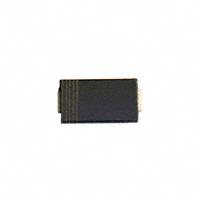


 工商网监
湘ICP备2023018690号
工商网监
湘ICP备2023018690号
