REVISIONS
LTR
DESCRIPTION
DATE (YR-MO-DA)
APPROVED
A
Changes in accordance with NOR 5962-R064-93. - drw
93-01-11
Michael A. Frye
B
Update drawing to current requirements. Editorial changes throughout. – drw
02-09-04
Raymond Monnin
C
Redrawn. Update paragraphs to MIL-PRF-38535 requirements. - drw
15-02-05
Charles F. Saffle
THE ORIGINAL FIRST SHEET OF THIS DRAWING HAS BEEN REPLACED.
REV
SHEET
REV
SHEET
REV STATUS
REV
C
C
C
C
C
C
C
C
C
C
C
C
OF SHEETS
SHEET
1
2
3
4
5
6
7
8
9
10
11
12
PMIC N/A
PREPARED BY
Gary Zahn
STANDARD
MICROCIRCUIT
DRAWING
DLA LAND AND MARITIME
COLUMBUS, OHIO 43218-3990
http://www.landandmaritime.dla.mil
CHECKED BY
Charles E. Besore
APPROVED BY
THIS DRAWING IS AVAILABLE
FOR USE BY ALL
DEPARTMENTS
AND AGENCIES OF THE
DEPARTMENT OF DEFENSE
AMSC N/A
William K. Heckman
DRAWING APPROVAL DATE
89-08-08
REVISION LEVEL
C
MICROCIRCUIT, LINEAR, CMOS,
MICROPROCESSOR COMPATIBLE, DUAL 12-BIT
DIGITAL-TO-ANALOG CONVERTERS,
MONOLITHIC SILICON
SIZE
CAGE CODE
A
67268
SHEET
DSCC FORM 2233
APR 97
5962-88765
1 OF 12
5962-E174-15
�1. SCOPE
1.1 Scope. This drawing describes device requirements for MIL-STD-883 compliant, non-JAN class level B microcircuits in
accordance with MIL-PRF-38535, appendix A.
1.2 Part or Identifying Number (PIN). The complete PIN is as shown in the following example:
5962-88765
01
R
A
Drawing number
Device type
(see 1.2.1)
Case outline
(see 1.2.2)
Lead finish
(see 1.2.3)
1.2.1 Device types. The device types identify the circuit function as follows:
Device type
Generic number
01
02
7549S
7549T
Circuit function
Relative accuracy
Dual, CMOS, 12-bit DAC
Dual, CMOS, 12-bit DAC
±1.0 LSB
±0.5 LSB
1.2.2 Case outline. The case outline is as designated in MIL-STD-1835 as follows:
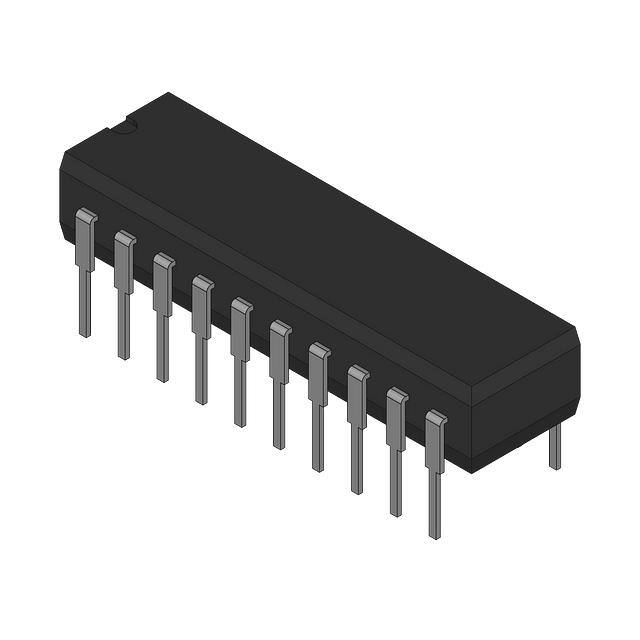
Outline letter
Descriptive designator
Terminals
Package style
R
GDIP1-T20 or CDIP2-T20
20
dual-in-line
1.2.3 Lead finish. The lead finish is as specified in MIL-PRF-38535, appendix A.
1.3 Absolute maximum ratings.
VDD to DGND ...................................................................................................
VREFA, VREFB to AGND ......................................................................................
VRFBA, VRFBB to AGND ......................................................................................
Digital input to DGND ......................................................................................
VPIN15, VPIN17 to DGND .....................................................................................
AGND to DGND ...............................................................................................
Storage temperature range..............................................................................
Lead temperature (soldering, 10 seconds) ......................................................
Power dissipation (PD) .....................................................................................
Thermal resistance, junction-to-case (θJC).......................................................
Thermal resistance, junction-to-ambient (θJA)..................................................
Junction temperature (TJ) ................................................................................
-0.3 V dc to +17 V dc
±25 V dc
±25 V dc
-0.3 V dc to VDD
-0.3 V dc to VDD
-0.3 V dc to VDD
-65°C to +150°C
+300°C
+450 mW 1/
See MIL-STD-1835
+120°C/W
+175°C
1.4 Recommended operating conditions.
Supply voltage (VDD) ........................................................................................
A-reference voltage (VREFA) .............................................................................
B-reference voltage (VREFB) .............................................................................
Ambient operating temperature range (TA) ......................................................
+14.25 V dc to +15.75 V dc
+10 V dc
+10 V dc
-55°C to +125°C
______
1/ Derate above TA = +75°C at +6.0 mW/°C.
STANDARD
MICROCIRCUIT DRAWING
DLA LAND AND MARITIME
COLUMBUS, OHIO 43218-3990
DSCC FORM 2234
APR 97
SIZE
5962-88765
A
REVISION LEVEL
C
SHEET
2
�2. APPLICABLE DOCUMENTS
2.1 Government specification, standards, and handbooks. The following specification, standards, and handbooks form a part
of this drawing to the extent specified herein. Unless otherwise specified, the issues of these documents are those cited in the
solicitation or contract.
DEPARTMENT OF DEFENSE SPECIFICATION
MIL-PRF-38535 - Integrated Circuits, Manufacturing, General Specification for.
DEPARTMENT OF DEFENSE STANDARDS
MIL-STD-883 MIL-STD-1835 -
Test Method Standard Microcircuits.
Interface Standard Electronic Component Case Outlines.
DEPARTMENT OF DEFENSE HANDBOOKS
MIL-HDBK-103 MIL-HDBK-780 -
List of Standard Microcircuit Drawings.
Standard Microcircuit Drawings.
(Copies of these documents are available online at http://quicksearch.dla.mil or from the Standardization Document Order
Desk, 700 Robbins Avenue, Building 4D, Philadelphia, PA 19111-5094.)
2.2 Order of precedence. In the event of a conflict between the text of this drawing and the references cited herein, the text
of this drawing takes precedence. Nothing in this document, however, supersedes applicable laws and regulations unless a
specific exemption has been obtained.
3. REQUIREMENTS
3.1 Item requirements. The individual item requirements shall be in accordance with MIL-PRF-38535, appendix A for nonJAN class level B devices and as specified herein. Product built to this drawing that is produced by a Qualified Manufacturer
Listing (QML) certified and qualified manufacturer or a manufacturer who has been granted transitional certification to
MIL-PRF-38535 may be processed as QML product in accordance with the manufacturers approved program plan and
qualifying activity approval in accordance with MIL-PRF-38535. This QML flow as documented in the Quality Management
(QM) plan may make modifications to the requirements herein. These modifications shall not affect form, fit, or function of the
device. These modifications shall not affect the PIN as described herein. A "Q" or "QML" certification mark in accordance with
MIL-PRF-38535 is required to identify when the QML flow option is used.
3.2 Design, construction, and physical dimensions. The design, construction, and physical dimensions shall be as specified
in MIL-PRF-38535, appendix A and herein.
3.2.1 Case outline. The case outline shall be in accordance with 1.2.2 herein.
3.2.2 Terminal connections. The terminal connections shall be as specified on figure 1.
3.2.3 Truth table. The truth table shall be as specified on figure 2.
3.3 Electrical performance characteristics. Unless otherwise specified herein, the electrical performance characteristics are
as specified in table I and shall apply over the full ambient operating temperature range.
3.4 Electrical test requirements. The electrical test requirements shall be the subgroups specified in table II. The electrical
tests for each subgroup are described in table I.
3.5 Marking. Marking shall be in accordance with MIL-PRF-38535, appendix A. The part shall be marked with the PIN
listed in 1.2 herein. In addition, the manufacturer's PIN may also be marked. For packages where marking of the entire SMD
PIN number is not feasible due to space limitations, the manufacturer has the option of not marking the "5962-" on the device.
3.5.1 Certification/compliance mark. A compliance indicator “C” shall be marked on all non-JAN devices built in compliance
to MIL-PRF-38535, appendix A. The compliance indicator “C” shall be replaced with a "Q" or "QML" certification mark in
accordance with MIL-PRF-38535 to identify when the QML flow option is used
STANDARD
MICROCIRCUIT DRAWING
DLA LAND AND MARITIME
COLUMBUS, OHIO 43218-3990
DSCC FORM 2234
APR 97
SIZE
5962-88765
A
REVISION LEVEL
C
SHEET
3
�TABLE I. Electrical performance characteristics.
Test
Symbol
Conditions 1/, 2/
-55°C ≤ TA ≤ +125°C
unless otherwise specified
Group A
subgroups
Device
type
Limits
Min
RES
Resolution
Relative accuracy
Guaranteed minimum
resolution
RA
DNL
Guaranteed monotonic to
12-bits
AE
Gain error 3/
All
12
1, 2, 3
01
±1.0
1
02
±1.0
Output leakage current
PSRR
full scale outputs
IOUTA
All
±1.0
LSB
1, 2, 3
01
±6.0
LSB
1
02
±6.0
±3.0
All
±0.01
2, 3
DAC A loaded with all 0’s
1
DAC B loaded with all 0’s
%/%
±0.02
All
20
2, 3
IOUTB
LSB
1, 2, 3
1
∆VDD = ±5.0%,
Bits
±0.5
2, 3, 12
Supply rejection
(∆Gain/∆VDD)
Max
1, 2, 3
2, 3, 12
Differential nonlinearity
Unit
nA
250
1
All
20
2, 3
nA
250
tSL
IOUT load = 100Ω,
CEXT = 13 pF, DAC output
measured from falling edge
of WR
4
All
1.5
µs
Feedthrough error, VREFA to
IOUTA or VREFB to IOUTB 4/, 5/
FT
VREFA = VREFB = ±20 Vpp,
10 kHz sine wave, DAC
register loaded with all 0’s
4
All
-65
dB
Reference input resistance
RIN
1, 2, 3
All
18
kΩ
RMIN
1, 2, 3
01
±3.0
%
1
02
±3.0
Output current settling time
to 0.01% of FSR 4/
Reference input resistance
match (VREFA/VREFB)
7.0
2, 3, 12
±2.0
See footnotes at end of table.
STANDARD
MICROCIRCUIT DRAWING
DLA LAND AND MARITIME
COLUMBUS, OHIO 43218-3990
DSCC FORM 2234
APR 97
SIZE
5962-88765
A
REVISION LEVEL
C
SHEET
4
�TABLE I. Electrical performance characteristics - continued.
Test
Symbol
Conditions 1/, 2/
-55°C ≤ TA ≤ +125°C
unless otherwise specified
Group A
subgroups
Device
type
Limits
Min
Unit
Max
Digital input high voltage
VIH
1, 2, 3
All
Digital input low voltage
VIL
1, 2, 3
All
0.8
V
Input leakage current
IIN
1
All
±1.0
µA
VIN = VDD
2.4
2, 3
Input capacitance 4/
Analog output capacitance
CIN
COUTA
4/
DAC A = all 0’s
±10
4
All
7.0
pF
4
All
80
pF
DAC A = all 1’s
Analog output capacitance
COUTB
DAC B = all 1’s
Functional test
See 4.3.1c
Address valid to write setup
time
tAWS
160
DAC B = all 0’s
4/
4
All
80
Data setup time
pF
160
See figure 3
7, 8
All
9
All
50
10, 11
Address valid to write hold
time
V
ns
110
tAWH
See figure 3
9, 10, 11
All
0
ns
tDS
See figure 3
9
All
180
ns
10, 11
240
Data hold time
tDH
See figure 3
9, 10, 11
All
5
ns
Chip select or update to
write setup time
Chip select or update to
write hold time
tCWS
See figure 3
9, 10, 11
All
20
ns
tCWH
See figure 3
9, 10, 11
All
0
ns
tWR
See figure 3
9
All
170
ns
Write pulse width
10, 11
250
See footnotes at end of table.
STANDARD
MICROCIRCUIT DRAWING
DLA LAND AND MARITIME
COLUMBUS, OHIO 43218-3990
DSCC FORM 2234
APR 97
SIZE
5962-88765
A
REVISION LEVEL
C
SHEET
5
�TABLE I. Electrical performance characteristics - continued.
Test
Symbol
Conditions 1/, 2/
-55°C ≤ TA ≤ +125°C
unless otherwise specified
Group A
subgroups
Device
type
Limits
Min
Clear pulse width
tCLR
See figure 3
9
All
IDD
1, 2, 3
Max
170
10, 11
Supply current
Unit
ns
250
All
5.0
mA
1/
VREFA = VREFB = +10 V, VPIN15 = VPIN16 = VPIN17 = 0 V unless otherwise specified. All tests are guaranteed over a supply
voltage range of VDD = 15 V ±5.0%, however, all measurements are made at VDD = +15 V unless otherwise specified.
2/
Subgroups 10 and 11, if not tested, shall be guaranteed to the limits specified in table I.
3/
Measured using internal feedback resistor and includes effects of leakage current and gain temperature coefficient.
4/
Subgroup 4 (tSL, FT, CIN, COUTA and COUTB measurements) shall be measured only for the initial test and after process or
design changes which may affect these tests.
5/
Feedthrough can be further reduced by connecting the metal lid to ground.
STANDARD
MICROCIRCUIT DRAWING
DLA LAND AND MARITIME
COLUMBUS, OHIO 43218-3990
DSCC FORM 2234
APR 97
SIZE
5962-88765
A
REVISION LEVEL
C
SHEET
6
�Device types
All
Case outline
R
Terminal
number
1
Terminal
symbol
DB3
2
DB2
3
DB1
4
DB0
5
UPD
6
A2
7
A1
8
A0
9
CS
10
11
WR
CLR
12
DGND
13
VREFB
14
RFBB
15
IOUTB
16
AGND
17
IOUTA
18
RFBA
19
VREFA
20
VDD
FIGURE 1. Terminal connections.
STANDARD
MICROCIRCUIT DRAWING
DLA LAND AND MARITIME
COLUMBUS, OHIO 43218-3990
DSCC FORM 2234
APR 97
SIZE
5962-88765
A
REVISION LEVEL
C
SHEET
7
�CLR
UPD
CS
WR
A2
A1
A0
Function
0
X
X
1
X
X
X
No data transfer
0
1
1
X
X
X
X
No data transfer
1
X
X
X
X
X
X
All register cleared
0
1
0
0
0
0
DAC A low nibble register loaded from data bus
0
1
0
0
0
1
DAC A mid nibble register loaded from data bus
0
1
0
0
1
0
DAC A high nibble register loaded from data bus
0
1
0
0
1
1
DAC A register loaded from input registers
0
1
0
1
0
0
DAC B low nibble register loaded from data bus
0
1
0
1
0
1
DAC B mid nibble register loaded from data bus
0
1
0
1
1
0
DAC B high nibble register loaded from data bus
0
1
0
1
1
1
DAC B register loaded from input registers
0
0
1
X
X
X
DAC A, DAC B registers updated simultaneously
from input registers
0 = Logic low level
1 = Logic high level
X = Don’t care
FIGURE 2. Truth table.
STANDARD
MICROCIRCUIT DRAWING
DLA LAND AND MARITIME
COLUMBUS, OHIO 43218-3990
DSCC FORM 2234
APR 97
SIZE
5962-88765
A
REVISION LEVEL
C
SHEET
8
�Notes:
1.
All input signal rise and fall times are measured from 10% to 90% of +5.0 V, tr = tf = 20 ns.
VIH + VIL
2.
Timing measurement reference level is
2
FIGURE 3. Timing diagram.
STANDARD
MICROCIRCUIT DRAWING
DLA LAND AND MARITIME
COLUMBUS, OHIO 43218-3990
DSCC FORM 2234
APR 97
SIZE
5962-88765
A
REVISION LEVEL
C
SHEET
9
�3.6 Certificate of compliance. A certificate of compliance shall be required from a manufacturer in order to be listed as an
approved source of supply in MIL-HDBK-103 (see 6.6 herein). The certificate of compliance submitted to DLA Land and
Maritime -VA prior to listing as an approved source of supply shall affirm that the manufacturer's product meets the
requirements of MIL-PRF-38535, appendix A and the requirements herein.
3.7 Certificate of conformance. A certificate of conformance as required in MIL-PRF-38535, appendix A shall be provided
with each lot of microcircuits delivered to this drawing.
3.8 Notification of change. Notification of change to DLA Land and Maritime -VA shall be required for any change that
affects this drawing.
3.9 Verification and review. DLA Land and Maritime, DLA Land and Maritime's agent, and the acquiring activity retain the
option to review the manufacturer's facility and applicable required documentation. Offshore documentation shall be made
available onshore at the option of the reviewer.
4. VERIFICATION
4.1 Sampling and inspection. Sampling and inspection procedures shall be in accordance with MIL-PRF-38535,
appendix A.
4.2 Screening. Screening shall be in accordance with method 5004 of MIL-STD-883, and shall be conducted on all devices
prior to quality conformance inspection. The following additional criteria shall apply:
a.
Burn-in test, method 1015 of MIL-STD-883.
(1) Test condition A, B, C, or D. The test circuit shall be maintained by the manufacturer under document revision level
control and shall be made available to the preparing or acquiring activity upon request. The test circuit shall specify
the inputs, outputs, biases, and power dissipation, as applicable, in accordance with the intent specified in method
1015 of MIL-STD-883.
(2) TA = +125°C, minimum.
b.
Interim and final electrical test parameters shall be as specified in table II herein, except interim electrical parameter
tests prior to burn-in are optional at the discretion of the manufacturer.
STANDARD
MICROCIRCUIT DRAWING
DLA LAND AND MARITIME
COLUMBUS, OHIO 43218-3990
DSCC FORM 2234
APR 97
SIZE
5962-88765
A
REVISION LEVEL
C
SHEET
10
�TABLE II. Electrical test requirements.
MIL-STD-883 test requirements
Interim electrical parameters
(method 5004)
Final electrical test parameters
(method 5004)
Group A test requirements
(method 5005)
Groups C and D end-point
electrical parameters
(method 5005)
Subgroups
(in accordance with
MIL-STD-883, method 5005,
table I)
--1*, 2, 3, 7, 12
1, 2, 3, 4**, 7, 8, 9, 10***,
11***, 12
1
*
PDA applies to subgroup 1.
** See 4.3.1e.
*** Subgroups 10 and 11, if not tested, shall be guaranteed to the
limits specified in table I.
4.3 Quality conformance inspection. Quality conformance inspection shall be in accordance with method 5005 of
MIL-STD-883 including groups A, B, C, and D inspections. The following additional criteria shall apply.
4.3.1 Group A inspection.
a.
Tests shall be as specified in table II herein.
b.
Subgroups 5 and 6 in table I, method 5005 of MIL-STD-883 shall be omitted.
c.
Subgroups 7 and 8 shall include verification of the truth table.
d.
Subgroup 12 test is used for grading and part selection at TA = +25°C and is not included in PDA calculations.
e.
Subgroup 4 (tSL, FT, CIN, COUTA and COUTB measurements) shall be measured only for the initial test and after process
or design changes which may affect these capacitance measurements.
4.3.2 Groups C and D inspections.
a.
End-point electrical parameters shall be as specified in table II herein.
b.
Steady-state life test conditions, method 1005 of MIL-STD-883.
(1)
Test condition A, B, C, or D. The test circuit shall be maintained by the manufacturer under document revision
level control and shall be made available to the preparing or acquiring activity upon request. The test circuit shall
specify the inputs, outputs, biases, and power dissipation, as applicable, in accordance with the intent specified in
method 1005 of MIL-STD-883.
(2)
TA = +125°C, minimum.
(3)
Test duration: 1,000 hours, except as permitted by method 1005 of MIL-STD-883.
STANDARD
MICROCIRCUIT DRAWING
DLA LAND AND MARITIME
COLUMBUS, OHIO 43218-3990
DSCC FORM 2234
APR 97
SIZE
5962-88765
A
REVISION LEVEL
C
SHEET
11
�5. PACKAGING
5.1 Packaging requirements. The requirements for packaging shall be in accordance with MIL-PRF-38535, appendix A.
6. NOTES
6.1 Intended use. Microcircuits conforming to this drawing are intended for use for Government microcircuit applications
(original equipment), design applications, and logistics purposes.
6.2 Replaceability. Microcircuits covered by this drawing will replace the same generic device covered by a contractorprepared specification or drawing.
6.3 Configuration control of SMD's. All proposed changes to existing SMD's will be coordinated with the users of record for
the individual documents. This coordination will be accomplished using DD Form 1692, Engineering Change Proposal.
6.4 Record of users. Military and industrial users shall inform DLA Land and Maritime when a system application requires
configuration control and the applicable SMD to that system. DLA Land and Maritime will maintain a record of users and this
list will be used for coordination and distribution of changes to the drawings. Users of drawings covering microelectronics
devices (FSC 5962) should contact DLA Land and Maritime-VA, telephone (614) 692-8108.
6.5 Comments. Comments on this drawing should be directed to DLA Land and Maritime-VA, Columbus, Ohio 43218-3990,
or telephone (614) 692-0540.
6.6 Approved sources of supply. Approved sources of supply are listed in MIL-HDBK-103 and QML-38535. The vendors
listed in MIL-HDBK-103 and QML-38535 have agreed to this drawing and a certificate of compliance (see 3.6 herein) has been
submitted to and accepted by DLA Land and Maritime-VA.
STANDARD
MICROCIRCUIT DRAWING
DLA LAND AND MARITIME
COLUMBUS, OHIO 43218-3990
DSCC FORM 2234
APR 97
SIZE
5962-88765
A
REVISION LEVEL
C
SHEET
12
�STANDARD MICROCIRCUIT DRAWING BULLETIN
DATE: 15-02-05
Approved sources of supply for SMD 5962-88765 are listed below for immediate acquisition information only and
shall be added to MIL-HDBK-103 and QML-38535 during the next revision. MIL-HDBK-103 and QML-38535 will be
revised to include the addition or deletion of sources. The vendors listed below have agreed to this drawing and a
certificate of compliance has been submitted to and accepted by DLA Land and Maritime-VA. This information
bulletin is superseded by the next dated revision of MIL-HDBK-103 and QML-38535. DLA Land and Maritime
maintains an online database of all current sources of supply at http://www.landandmaritime.dla.mil/Programs/Smcr/.
Standard
microcircuit drawing
PIN 1/
Vendor
CAGE
number
Vendor
similar
PIN 2/
5962-8876501RA
24355
AD7549SQ/883B
5962-8876502RA
24355
AD7549TQ/883B
1/ The lead finish shown for each PIN representing
a hermetic package is the most readily available
from the manufacturer listed for that part. If the
desired lead finish is not listed contact the vendor
to determine its availability.
2/ Caution. Do not use this number for item
acquisition. Items acquired to this number may not
satisfy the performance requirements of this drawing.
Vendor CAGE
number
24355
Vendor name
and address
Analog Devices
Rt 1 Industrial Park
PO Box 9106
Norwood, MA 02062
Point of contact:
Raheen Business Park
Limerick, Ireland
The information contained herein is disseminated for convenience only and the
Government assumes no liability whatsoever for any inaccuracies in the
information bulletin.
�


 工商网监
湘ICP备2023018690号
工商网监
湘ICP备2023018690号
