Isolated Linearized RTD Input
5B34
FEATURES
FUNCTIONAL BLOCK DIAGRAM
Amplifies, Protects, Filters, and Isolates Analog Input.
Linearize a wide variety of 2 & 3 wire RTDs. (True 4-wire RTD
measurements are provided by the 5B35).
Generates an output of 0 to +5V.
Module circuitry can withstand 240v rms at the input screwterminals.
All 5B34 series modules are mix-and-match and Hot
Swappable.
APPLICATIONS
Industrial signal conditioning
Industrial signal isolation
Industrial signal filtering
Signal Linearization
PRODUCT OVERVIEW
The 5B Series represents an innovative generation of low cost,
high performance plug-in signal conditioners. Designed for
industrial applications, these modules incorporate highly
reliable transformer-based isolation and automated surfacemount manufacturing technology. They are compact,
economical components whose performance exceeds that
available from more expensive devices. Combining 1500 V rms
continuous isolation, +0.05% calibrated accuracy, small size and
low cost, the 5B Series is an attractive alternative to expensive
signal conditioners and in-house designs
All modules are potted and identical in pin-out and size (2.27” x
2.32” x 0.595”). They can be mixed and matched, permitting
users to address their exact needs, and may be “hot swapped
without disturbing field wiring or power. The isolated input
modules provide 0 to +5V or +5V outputs and accept J, K, T, E,
R, S, N, or B type thermocouples.
These modules feature complete signal conditioning functions
including 240 V rms input protection, filtering, chopper
stabilized low drift +1 uV/oC amplification, 1500 V rms
isolation, and sensor excitation when required.
All modules feature excellent common mode rejection and
meet industrial transient surge withstand specifications.
Figure 1. 5B34 Functional Block Diagram
There are also a number of backplanes and mounting sockets
which provide a complete signal conditioning solution for end
users. Each backplane incorporates screw terminals for field
wiring inputs and outputs and cold junction sensors for
thermocouple applications.
These signal conditioners are designed to provide an easy and
convenient solution to signal conditioning problems of both
designers and end users in measurement and control
applications. Typical uses include microcomputer-based
measurement systems, standard data acquisition systems,
programmable controllers, analog recorders and dedicated
control systems. The 5 B series modules are ideally suited to
applications where monitoring and control of temperature,
pressure, flow, rotation and other analog signals are required.
The 5B Series modules and backplanes are approved by Factory
Mutual (FM) and the 5B Series modules are approved by the
Canadian Standards Association (CSA) for use in Class 1,
Division 2, Groups A, B, C, and D locations. These approvals
certify that the 5B Series is suitable for use in locations where a
hazardous concentration of flammable gas may exist only under
fault conditions of operation. Equipment of this category is
called “non-incendive” and they need no special enclosures or
other physical safeguards. The 5B series modules and
backplanes have been tested and passed the stringent heavy
industrial requirements of the EU’s electromagnetic
compatibility (ENC) directive – EN50082-1 and EN50081-2.
When used according to installation directions (refer to 5B
series User Manual), any errors caused by EMI/RFI interference
will be less than 0.1% of the full scale 5B measurement range for
field strengths up to 10 V/M and frequencies up to 1 GHz.
Rev. 0
Information furnished by Analog Devices is believed to be accurate and reliable.
However, no responsibility is assumed by Analog Devices for its use, nor for any
infringements of patents or other rights of third parties that may result from its use.
Specifications subject to change without notice. No license is granted by implication
or otherwise under any patent or patent rights of Analog Devices. Trademarks and
registered trademarks are the property of their respective companies.
One Technology Way, P.O. Box 9106, Norwood, MA 02062-9106, U.S.A.
www.analog.com
Tel: 781.329.4700
Fax: 781.326.8703
© 2004 Analog Devices, Inc. All rights reserved.
�5B34
GENERAL DESCRIPTION
measurement accuracy. Along with module gain and zero
settings, a feedback linearizer is laser-trimmed. Custom versions
of 5N34 can be laser-trimmed to meet special requirements.
The 5B34 is a single-channel signal conditioning module that
amplifies, protects, filters, linearizes, and isolates a wide variety
of two and three-wire RTDs. For true four-wire RTD
measurements please refer to the 5B35 model.
Internal multi-pole low-pass filtering with a four-Hz cutoff (3dB) enhances normal-mode (noise on signal) and commonmode (noise on signal return) rejection at 50/60 Hz, enabling
accurate measurement of small signals in high electrical noise.
The 5B34 protects the computer side from damage due to fieldside over-volatge faults. The module withstands 240 V rms at
the input terminals without damage thereby shielding the
internal computer-side circuitry from field-side over-voltage
conditions. In addition, the 5B34 is mix-and-match and hot
swappable with all other 5B Series input modules, so can be
inserted or removed from any socket in the same backplane
without disrupting system power.
Signal isolation by transformer coupling uses a proprietary
modulation technique for linear, stable and reliable
performance. The differential input circuit on the field side is
fully floating, eliminating the need for any input grounding. A
demodulator on the computer side of the signal transformer
recovers the original signal, which is then filtered and buffered
to provide a low-noise, low-impedance output signal. The
output common must be kept within +3V of power common.
Two identical sources provide excitation current for the RTD.
For three-wire RTDs, the second current flows through the
third RDT lead so as to cancel the effects of (equal) lead
resistance; this current also flows through a stable resistor lasertrimmed to the RTD value that sets the differential amplifier
input and (module) output to zero volts at that scale point. The
current sources and the amplifier input are protected to
withstand input over-voltage up to 240 V rms.
A series output switch eliminates the need for external
multiplexing in many applications. The switch is turned on by
an active-low enable input. If the switch is to be on at all times,
the enable-input should be grounded to power common as it is
on the 5B01 and 5B08 backplanes.
A differential chopper-stabilized input amplifier provides stable
gain and exceptionally low drift. This allows the use of very low
RTD excitation current to minimize self-heating and preserve
.
.
Figure 2
Rev. 0 | Page 2 of 8
�5B34
5B34—SPECIFICATIONS
5B34 Models Available
Model
Input Range
Output Range
Accuracy
5B34-01
100 Ω Platinum,
= 0.00385*
-100°C to +100°C (-148°F to +212°F)
0 V to +5 V
±0.32°C
5B34-02
0°C to +100°C (+32°F to 212°F)
0 V to +5 V
±0.13°C
5B34-03
0°C to +200°C (+32°F to 392°F)
0 V to +5 V
±0.26°C
5B34-04
0°C to +600°C (+32°F to 1112°F)
0 V to +5 V
±0.78°C
0 V to +5 V
±0.23°C
5B34-C-01
= 0.004274
10Ω Copper,
0°C to +120°C (10Ω @ 0°C) (+32°F to +248°F)
5B34-C-02
0°C to +120°C (10Ω @ 25°C)(+32°F to +248°F)
0 V to +5 V
±0.23°C
5B34-N-01
120Ω Nickel, * = 0.00672
0°C to +300°C (+32°F to +572°F)
0 V to +5 V
±0.40°C
5B34-Custom
*
*
* Custom Input/Output ranges are available including versions for the 100Ω Platinum RTD with
Refer to configuration guide.
=0.003916.
5B34 Specifications
(typical @ +25°C and Vs = +5 V dc)
Description
Model 5B34
Input Ranges
Standard Ranges
Refer to Model Table
Custom Ranges
-200°C to +850°C (100Ω Platinum)
-80°C to +320°C (120Ω Nickel)
-100°C to +260°C (10Ω Copper)
Output Range (RL > 50 kΩ)
0 V to +5 V
Accuracy2
Initial @ +25°C
±0.05% Span ±0.04Ω * ±0.05 (Rz1)
Conformity Error3
±0.05% Span
Input Offset vs. Temperature
±0.02°C/°C
Output Offset vs. Temperature
±20 µV/°C
Gain vs. Temperature
±0.005% of Reading/°C
Input Bias Current
±3 nA
Input Resistance
Power On
5 MΩ
Power Off
40 kΩ
Overload
40 kΩ
Noise
Input, 0.1 Hz to 10 Hz Bandwidth
0.2 µV rms
Output, 100 kHz Bandwidth
200 µV rms
Bandwidth, -3 dB
4 Hz
Rev. 0 | Page 3 of 8
�5B34
Output Rise Time, 10% to 90% Span
200 ms
Common-Mode Voltage (CMV)
Input-to-Output, Continuous
1500 V rms, maximum
4
Output-to-Power, Continuous
±3 V, maximum
Transient
ANSI/IEEE C37.90.1-1989
Common Mode Rejection (CMR)
1 kΩ Source Imbalance, 50/60 Hz
160 dB
Normal Mode Rejection 50/60 Hz
60 dB
Sensor Excitation Current
100Ω Pt, 120Ω Ni
0.25 mA
10Ω Cu
1.0 mA
Lead Resistance Effect
100Ω Pt, 120Ω Ni
±0.02°C/Ω
10Ω Cu
±0.2°C/Ω
Input Protection
Continuous
240 V rms, maximum
Transient
ANSI/IEEE C37.90.1-1989
Output Resistance
50Ω
Voltage Output Protection
Continuous Short to Ground
Output Selection Time
6 µs @ Cload = 0 to 2,000 pF
Max Logic "0"
+1 V
Min Logic "1"
+2.5 V
Max Logic "1"
+36 V
Input Current "0"
0.4 mA
Power Supply Voltage
+5 V ±5%
Power Supply Current
30 mA
Output Enable Control
Power Supply Sensitivity, RTI
100Ω Pt, 120Ω Ni
±0.05°C/V
10Ω Cu
±0.5°C/V
Mechanical Dimensions
2.275" x 2.375" x 0.595" (57.8 mm x 59.1 mm x 15.1 mm)
Environmental
Rated Performance
-25°C to +85°C
Operating
-40°C to +85°C
Storage
-40°C to +85°C
Relative Humidity
0 to 93% @ +40°C non-condensing
RFI Susceptibility
±0.5% Span error @ 400 MHz, 5 Watt, 3 ft
* ±0.025Ω For Cu RTD's; ±0.1Ω For Ni RTD's.
Rz is the value of the RTD resistance at the lowest point of the measurement range.
Includes the combined effects of repeatability, hysteresis,
and conformity error. Loads heavier than 50 kΩ will degrade conformity and gain temperature coefficient.
3
For Pt RTD's only; other types may vary.
4
The output common must be kept within ±3 V of power common.
Specifications subject to change without notice.
1
2
Rev. 0 | Page 4 of 8
�5B34
PIN CONFIGURATIONS AND FUNCTIONAL DESCRIPTIONS
Figure 3 5B34 Input Field Connections
Table 1. Pin Function Descriptions—
Pin No.
1
2
3
4
Description
NC
LO
HI
RETURN
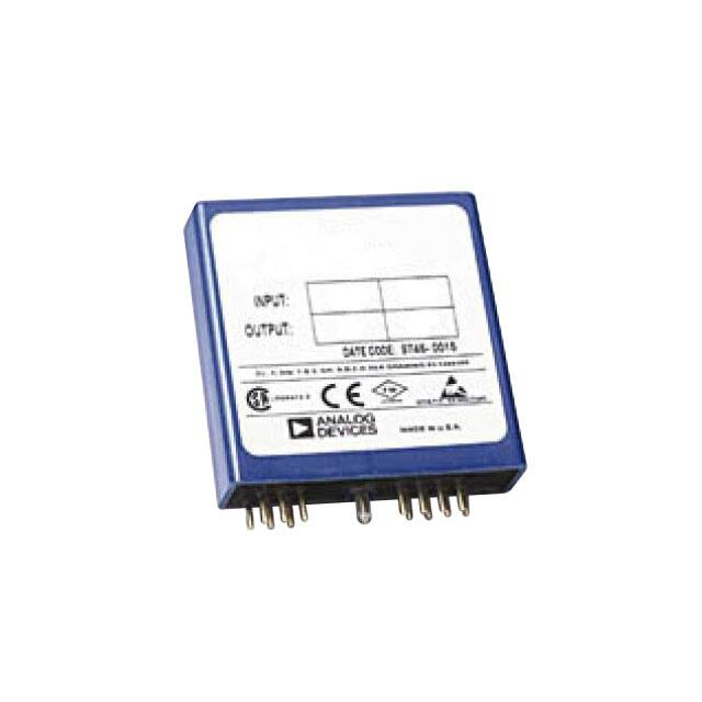
Figure 4 . Model 5B Series Module, with pin-out assignments.
ESD CAUTION
ESD (electrostatic discharge) sensitive device. Electrostatic charges as high as 4000 V readily accumulate on the human
body and test equipment and can discharge without detection. Although this product features proprietary ESD
protection circuitry, permanent damage may occur on devices subjected to high energy electrostatic discharges.
Therefore, proper ESD precautions are recommended to avoid performance degradation or loss of functionality.
Rev. 0 | Page 5 of 8
�5B34
OUTLINE DIMENSIONS
Figure 5. Outline Dimensions
Rev. 0 | Page 6 of 8
�5B34
NOTES
Rev. 0 | Page 7 of 8
�5B34
NOTES
© 2004 Analog Devices, Inc. All rights reserved. Trademarks and
registered trademarks are the property of their respective companies.
D05096-0-9/04(0)
Rev. 0 | Page 8 of 8
�


 工商网监
湘ICP备2023018690号
工商网监
湘ICP备2023018690号
