a
5 MHz–500 MHz 100 dB Demodulating
Logarithmic Amplifier with Limiter Output
AD8309
FEATURES
Complete Multistage Log-Limiting IF Amplifier
100 dB Dynamic Range: –78 dBm to +22 dBm (Re 50 ⍀)
Stable RSSI Scaling Over Temperature and Supplies:
20 mV/dB Slope, –95 dBm Intercept
ⴞ0.4 dB RSSI Linearity up to 200 MHz
Programmable Limiter Gain and Output Current
Differential Outputs to 10 mA, 2.4 V p-p
Overall Gain 100 dB, Bandwidth 500 MHz
Constant Phase (Typical ⴞ80 ps Delay Skew)
Single Supply of +2.7 V to +6.5 V at 16 mA Typical
Fully Differential Inputs, RIN = 1 k⍀, CIN = 2.5 pF
500 ns Power-Up Time, 4.5 V. For frequencies
in the range 10 MHz to 200 MHz these high drive levels are
easily achieved using a matching network (see later). Using such
a network, having an inductor at the input, the input transient is
eliminated.
The supply current for all sections except the limiter output
stage, and with no load attached to the RSSI output, is nominally 16 mA at TA = 27°C, substantially independent of supply
voltage. It varies in direct proportion to the absolute temperature (PTAT). The RSSI load current is simply the voltage at
VLOG divided by the load resistance (e.g., 2.4 mA max in a
1 kΩ load). The limiter supply current is 1.1 times that flowing
in RLIM. The AD8309 may be enabled/disabled by a CMOScompatible level at ENBL (Pin 8).
VPS1
TO STAGES
1 THRU 5
67V
S
1.78V
3.65kV
In the following simplified interface diagrams, the components
denoted with an uppercase “R” are thin-film resistors having a
very low temperature-coefficient of resistance and high linearity
under large-signal conditions. Their absolute value is typically
within ± 20%. Capacitors denoted using an uppercase “C” have
a typical tolerance of ± 15% and essentially zero temperature or
voltage sensitivity. Most interfaces have additional small junction capacitances associated with them, due to active devices or
ESD protection; these may be neither accurate nor stable. Component numbering in each of these interface diagrams is local.
CC
INHI
SIGNAL
INPUT
CC INLO
1.725V
RIN = 1kV
67V
3.65kV
IB = 15mA
CD
2.5pF
Q1
TO 2ND
STAGE
20e
RIN = 3kV
1.725V
Q2
20e
2.6kV
GAIN BIAS
1.26V
(TOP-END
DETECTORS)
CP
CP
130V
3.4mA
PTAT
COMM
Figure 27. Signal Input Interface
Enable Interface
The chip-enable interface is shown in Figure 26. The current in
R1 controls the turn-on and turn-off states of the band-gap
reference and the bias generator, and is a maximum of 100 µA
when Pin 8 is taken to 5 V. Left unconnected, or at any voltage
below 1 V, the AD8309 will be disabled, when it consumes a
sleep current of much less than 1 µA (leakage currents only); when
tied to the supply, or any voltage above 2 V, it will be fully enabled. The internal bias circuitry requires approximately 300 ns
for either OFF or ON, while a delay of some 6 µs is required for
the supply current to fall below 10 µA.
ENBL
R1
60kV
TO BIAS
ENABLE
1.3kV
50kV
4kV
COMM
Limiter Output Interface
The simplified limiter output stage is shown in Figure 28. The
bias for this stage is provided by a temperature-stable reference
voltage of nominally 400 mV which is forced across the external
resistor RLIM connected from Pin 9 (LMDR, or limiter drive) by
a special op amp buffer stage. The biasing scheme also introduces a slight “lift” to this voltage to compensate for the finite
current gain of the current source Q3 and the output transistors
Q1 and Q2. A maximum current of 10 mA is permissible (RLIM
= 40 Ω). In special applications, it may be desirable to modulate
the bias current; an example of this is provided in the Applications section. Note that while the bias currents are temperature
stable, the ac gain of this stage will vary with temperature, by
–6 dB over a 120°C range.
A pair of supply and temperature stable complementary currents
is generated at the differential output LMHI and LMLO (Pins
12 and 13), having a square wave form with rise and fall times
of typically 0.4 ns, when load resistors of 50 Ω are used. The
voltage at these output pins may swing to 1.2 V below the supply voltage applied to VPS2 (Pin 15).
Figure 26. Enable Interface
–12–
REV. B
�AD8309
Because of the very high gain bandwidth product of this amplifier considerable care must be exercised in using the limiter
outputs. The minimum necessary bias current and voltage
swings should be used. These outputs are best utilized in a fullydifferential mode. A flux-coupled transformer, a balun, or an
output matching network can be selected to transform these
voltages to a single-sided form. Equal load resistors are recommended, even when only one output pin is used, and these
should always be returned to the same well decoupled node on
the PC board. When the AD8309 is used only to generate an
RSSI output, the limiter should be completely disabled by omitting RLIM and strapping LMHI and LMLO to VPS2.
VPS2
1.3kV
LMHI
LMLO
1.3kV
Q1
Q2
4e
400mV
OA ZERO-TC
Q3
2.6kV
1.3kV
1.3kV
COM1
RLIM
Figure 28. Limiter Output Interface
RSSI Output Interface
The outputs from the ten detectors are differential currents,
having an average value that is dependent on the signal input
level, plus a fluctuation at twice the input frequency. The currents are summed at the internal nodes LGP and LGN shown in
Figure 29. A further current ITC is added to LGP, to position
the intercept to –108 dBV, by raising the RSSI output voltage
for zero input, and to provide temperature compensation , resulting in a stable intercept. For zero signal conditions, all the
detector output currents are equal. For a finite input, of either
polarity, their difference is converted by the output interface to
a single-sided voltage nominally scaled 20 mV/dB (400 mV per
decade), at the output VLOG (Pin 16). This scaling is controlled by a separate feedback stage, having a tightly controlled
transconductance. A small uncertainty in the log slope and
intercept remains (see Specifications); the intercept may be
adjusted (see Applications).
VPS2
SUMMED 1.3kV
DETECTOR
OUTPUTS
1.3kV
ISOURCE
>50mA
ON DEMAND
FLTR
C1
3.5pF
LGP
LGN
IT
3.3kV
VLOG
250ms
3.3kV
ISINK
FIXED
1mA
CF
VLOG
20mV/dB
125mA
COMM
TRANSCONDUCTANCE
DETERMINES SLOPE
Figure 29. Simplified RSSI Output Interface
REV. B
12.7 × 10⁻¹⁰
– 3.5 pF ;
f LP
f LP =
12.7 × 10⁻⁶
CF + 3.5 pF
(7)
Using a load resistance of 50 Ω or greater, and at any temperature, the peak output voltage may be at least 2.4 V when using a
supply of 4.5 V, and at least 2.1 V for a 3 V supply, which are
consistent with the maximum permissible input levels. The incremental output resistance is approximately 0.3 Ω at low frequencies, rising to 1 Ω at 150 kHz and 18 Ω at very high frequencies.
USING THE AD8309
LMDR
CURRENT
MIRROR
CF =
The output is unconditionally stable with load capacitance, but
it should be noted while the peak sourcing current is over 100 mA,
and able to rapidly charge even large capacitances, the internally
provided sinking current is only 1 mA. Thus, the fall time from
the 2 V level will be as long as 2 µs for a 1 nF load. This may be
reduced by adding a grounded load resistance.
4e
FROM FINAL
LIMITER STAGE
The RSSI output bandwidth, fLP, is nominally 3.5 MHz. This is
controlled by the compensation capacitor C1, which may be
increased by adding an external capacitor, CF, between FLTR
(Pin 10) and VLOG (Pin 16). An external 33 pF will reduce fLP
to 350 kHz, while 360 pF will set it to 35 kHz, in each case with
an essentially one-pole response. In general, the relationships
are:
The AD8309 exhibits very high gain from 1 MHz to over 1 GHz,
at which frequency the gain of the main path is still over 65 dB.
Consequently, it is susceptible to all signals within this very
broad frequency range which find their way to the input terminals. It is important to remember that these are quite indistinguishable from the “wanted” signal, and will have the effect of
raising the apparent noise floor (that is, lowering the useful
dynamic range). Therefore, while the signal of interest may be
an IF of, say, 200 MHz, any of the following could easily be
larger than this signal at the lower extremities of its dynamic
range: a 60 Hz hum, picked up due to poor grounding techniques; spurious coupling from digital logic on the same PC
board; a strong EMI source; etc.
Very careful shielding is essential to guard against such unwanted signals, and also to minimize the likelihood of instability
due to HF feedback from the limiter outputs to the input. With
this in mind, the minimum possible limiter gain should be used.
Where only the logarithmic amplifier (RSSI) function is required, the limiter should be disabled by omitting RLIM and
tying the outputs LMHI and LMLO directly to VPS2.
A good ground plane should be used to provide a low impedance connection to the common pins, for the decoupling
capacitor(s) used at VPS1 and VPS2, and at the output ground.
It is inadvisable to assume that any ground plane is an equipotential, however, and neither of the signal inputs should be accoupled directly to it, but kept separate, being returned instead
to the “low” associated with the source. This requires isolating
the “low”’ side of an input connector with a small resistance to
the ground plane. Note that COM2 is a special ground pin
serving just the RSSI output.
The voltages at the two supply pins should not be allowed to
differ greatly; up to 500 mV is permissible It is desirable to
allow VPS1 to be slightly more negative than VPS2. When the
primary supply is greater than 2.7 V, the decoupling resistors R1
and R2 may be increased to improve the isolation and lower
dissipation in the IC. However, since VPS2 supports the RSSI
–13–
�AD8309
2.5
The four pins labeled PADL tie down directly to the metallic
lead frame, and are thus connected to the back of the chip. The
process on which the AD8309 is fabricated uses a bonded-wafer
technique to provide a silicon-on-insulator isolation, and there is
no junction or other dc path from the back side to the circuitry
on the surface. These paddle pins must be connected directly to
the ground plane using the shortest possible lead lengths to
minimize inductance.
2.0
RSSI OUTPUT – V
load current, which may be large, the value of R2 should take
this into account.
Figure 30 shows the connections required for most applications.
The inputs are ac-coupled by C1 and C2, which normally
should have the same value, say, CO. The coupling time constant is ROCO /2, where RO = RS + RIN, thus forming a high pass
corner with a 3 dB attenuation at fHP = 1/(π RT CC ). In highfrequency applications, fHP should be chosen as large as possible, to minimize the coupling of unwanted signals. On the
other hand, in low frequency applications, a simple RC network
forming a low-pass filter should be added at the input for the
same reason.
1 COM2
SEE TEXT FOR MORE
ABOUT DECOUPLING 0.1mF
VLOG 16
2 VPS1
VPS2 15
3 PADL
PADL 14
LMHI
4 INHI
LMHI 13
RLOAD
5 INLO
LMLO 12
RLOAD
6 PADL
PADL 11
7 COM1
FLTR 10 NC
RLIM
LMDR 9
40
5
4
3
5MHz
DYNAMIC RANGE
5MHz
50MHz
100MHz
200MHz
1dB
85
91
97
96
3dB
93
99
103
102
1
50MHz
0
–1
100MHz 200MHz
–3
LMLO
8 ENBL
–4
–5
–90 –80 –70 –60 –50 –40 –30 –20 –10 0
INPUT LEVEL – dBm Re 50V
52.3V
ENABLE
20
–2
RT
4.7nH
–60
–40
–20
0
INPUT LEVEL – dBm Re 50V
2
RSSI
AD8309
–80
Figure 31. RSSI Output vs. Input Level at TA = +25 °C, for
Frequencies of 5 MHz, 50 MHz, 100 MHz and 200 MHz
VS
R2
10V
0.1mF
C1
FOR BROADBAND 50V
TERMINATION TO 1GHz
1.0
0
–100
ERROR – dB
R1
10V
C2
1.5
0.5
Basic Connections
SIGNAL
INPUTS
100MHz
50MHz
200MHz
5MHz
10
20
30
Figure 32. Log Linearity vs. Input Level at TA = +25 °C, for
Frequencies of 5 MHz, 50 MHz, 100 MHz and 200 MHz
NC = NO CONNECT
Input Matching
Figure 30. Basic Connections
Where either a higher sensitivity or a better high frequency
match is required, an input matching network is valuable. Using
a flux-coupled transformer to achieve the impedance transformation also eliminates the need for coupling capacitors, lowers
any dc offset voltages generated directly at the input, and usefully balances the drives to INHI and INLO, permitting full
utilization of the unusually large input voltage capacity of the
AD8309.
Where it is necessary to terminate the source at a low impedance, the resistor RT should be added, with allowance for the
shunting effect of the 1 kΩ input resistance (RIN) of the AD8309.
For example, to terminate a 50 Ω source, a 52.3 Ω␣ resistor
should be used for signal frequencies up to about 50 MHz. The
termination means may be placed either at the input or at the
log amp side of the coupling capacitors. In the former case
smaller capacitors can be used for a given frequency range; in
the latter case, the dc resistance is lowered directly at the log
amp inputs, which helps to keep offsets to a minimum. At
higher frequencies, the reactance of the 2.5 pF input capacitance must be accounted for. A 4.7 nH inductor in series with
the 52.3 Ω termination resistor provides an essentially flat 50 Ω
input impedance to 1 GHz. An impedance-transforming network is preferably used to provide a 50 Ω interface, since this
also introduces a balanced voltage gain of typically 13 dB and
the AD8309 has a very high capacity for large input voltages.
Figure 31 shows the output versus the input level, with the axis
marked in dBm (correct only when terminated in 50 Ω), for sine
inputs at 5 MHz, 50 MHz, 100 MHz and 200 MHz. Figure 32
shows the typical logarithmic linearity (law conformance) under
the same conditions.
The choice of turns ratio will depend somewhat on the frequency. At frequencies below 30 MHz, the reactance of the
input capacitance is much higher than the real part of the input
impedance. In this frequency range, a turns ratio of 2:9 will
lower the effective input impedance to 50 Ω while raising the
input voltage by 13 dB. However, this does not lower the effect
of the short circuit noise voltage by the same factor, since there
will be a contribution from the input noise current. Thus, the
total noise will be reduced by a smaller factor. The intercept at
the primary input will be lowered to –120 dBV (–107 dBm).
Impedance matching and drive balancing using a flux-coupled
transformer is useful whenever broadband coupling is required.
However, this may not always be convenient. At high frequencies, it will often be preferable to use a narrow-band matching
network, as shown in Figure 33, which has several advantages.
First, the same voltage gain can be achieved, providing increased
–14–
REV. B
�AD8309
sensitivity, but now a measure of selectively is simultaneously
introduced. Second, the component count is low: two capacitors
and an inexpensive chip inductor are needed. Third, the network also serves as a balun. Analysis of this network shows that
the amplitude of the voltages at INHI and INLO are quite similar when the impedance ratio is fairly high (say, 50 Ω to 1000 Ω).
14
13
12
11
DECIBELS
10
VS
10V
10V
1 COM2
VPS2 15
3 PADL
PADL 14
7
6
5
INPUT AT
TERMINATION
3
RSSI
0.1mF
2 VPS1
9
8
4
VLOG 16
0.1mF
GAIN
2
1
0
C1 = CM
ZIN
–1
60
AD8309
4 INHI
LMHI 13
5 INLO
LMLO 12
LIMITER
OUTPUT
LM
C2 = CM
PADL 11
7 COM1
FLTR 10 NC
RLIM
LMDR 9
130
140
150
Figure 34. Response of 100 MHz Matching Network
Step 1: Tune Out CIN
Figure 33. High Frequency Input Matching Network
Figure 34 shows the response for a center frequency of 100 MHz.
The response is down by 50 dB at one-tenth the center frequency,
falling by 40 dB per decade below this. The very high frequency
attenuation is relatively small, however, since in the limiting
case it is determined simply by the ratio of the AD8309’s input
capacitance to the coupling capacitors. Table I provides solutions for a variety of center frequencies fC and matching from
impedances ZIN of nominally 50 Ω and 100 Ω. Exact values are
shown, and some judgment is needed in utilizing the nearest
standard values.
At a center frequency fC, the shunt impedance of the input
capacitance CIN can be made to disappear by resonating with a
temporary inductor LIN, whose value is given by
LIN = 1/{(2 π fC)2CIN} = 1010/fC2
fC
MHz
Match to 50 ⍀
(Gain = 13 dB)
CM
LM
pF
nH
Match to 100 ⍀
(Gain = 10 dB)
CM
LM
pF
nH
10
10.7
15
20
21.4
25
30
35
40
45
50
60
80
100
120
150
200
250
300
350
400
450
500
140
133
95.0
71.0
66.5
57.0
47.5
40.7
35.6
31.6
28.5
23.7
17.8
14.2
11.9
9.5
7.1
5.7
4.75
4.07
3.57
3.16
2.85
100.7
94.1
67.1
50.3
47.0
40.3
33.5
28.8
25.2
22.4
20.1
16.8
12.6
10.1
8.4
6.7
5.03
4.03
3.36
2.87
2.52
2.24
2.01
4790
4460
3120
2290
2120
1790
1460
1220
1047
912
804
644
448
335
261
191
125
89.1
66.8
52.1
41.8
34.3
28.6
(8)
when CIN = 2.5 pF. For example, at fC = 100 MHz, LIN = 1 µH.
Step 2: Calculate CO and LO
Now having a purely resistive input impedance, we can calculate
the nominal coupling elements CO and LO, using
CO =
Table I.
REV. B
90
100
110
120
FREQUENCY – MHz
For other center frequencies and source impedances, the following
method can be used to calculate the basic matching parameters.
NC = NO CONNECT
3500
3200
2250
1660
1550
1310
1070
904
779
682
604
489
346
262
208
155
104
75.3
57.4
45.3
36.7
30.4
25.6
80
General Matching Procedure
6 PADL
8 ENBL
70
1
2 πfC
(R
IN RM
)
; LO =
(R
IN RM
)
2 πfC
(9)
For the AD8309, RIN is 1 kΩ. Thus, if a match to 50 Ω is
needed, at fC = 100 MHz, CO must be 7.12 pF and LO must be
356 nH.
Step 3: Split CO Into Two Parts
Since we wish to provide the fully-balanced form of network
shown in Figure 33, two capacitors C1 = C2 each of nominally
twice CO, shown as CM in the figure, can be used. This requires
a value of 14.24 pF in this example. Under these conditions, the
voltage amplitudes at INHI and INLO will be similar. A somewhat better balance in the two drives may be achieved when C1
is made slightly larger than C2, which also allows a wider range
of choices in selecting from standard values. For example, capacitors of C1 = 15 pF and C2 = 13 pF may be used (making
CO = 6.96 pF).
Step 4: Calculate LM
The matching inductor required to provide both LIN and LO is
just the parallel combination of these:
LM = LINLO/(LIN + LO)
(10)
With LIN = 1 µH and LO = 356 nH, the value of LM to complete
this example of a match of 50 Ω at 100 MHz is 262.5 nH. The
nearest standard value of 270 nH may be used with only a slight
loss of matching accuracy. The voltage gain at resonance depends only on the ratio of impedances, as is given by
R
IN
GAIN = 20 log
R
S
–15–
RIN
= 10 log
RS
(11)
�AD8309
Slope and Intercept Adjustment
VS
10V
The AD8309 provides limited opportunities for adjustment of
its basic scaling parameters, which are controlled to within tight
limits through robust design. In applications involving the observation of measured signal levels on a DVM a slope of 10 mV
per decade is convenient: the reading is then directly in decibels, needing only the positioning of the decimal point. This
may be simply achieved and at the same time trimmed to this
exact value using the scheme shown in Figure 35. A large filter
capacitor CFILT may be added as shown when the voltage is to
be measured on a DVM; this lowers the fluctuation in the lowerorder display digits.
VS
10V
10V
1 COM2
VLOG 16
2 VPS1
VPS2 15
3 PADL
PADL 14
8.87kV
AD8309
INPUT
COUPLING
4 INHI
LMHI 13
5 INLO
LMLO 12
6 PADL
PADL 11
7 COM1
FLTR 10
8 ENBL
0.1mF
LMDR 9
0.1mF
CFILT
10mF
VR1
2kV
SLOPE
RSSI OUTPUT
10mV/dB 6 10%
8.87kV
DVM
LIMITER
MAY BE
DISABLED
FOR RSSI
ONLY MODE
VPS2 15
3 PADL
PADL 14
RSSI
0.1mF
IN914
OR SIMILAR
4 INHI
LMHI 13
5 INLO
LMLO 12
6 PADL
PADL 11
7 COM1
FLTR 10
VR2
2kV
INTERCEPT
47kV
8 ENBL
LMDR 9
9.6kV
RLIM
Figure 36. Trimming Intercept to –113 dBV ± 4 dB
APPLICATIONS
The AD8309 is a versatile and easily applied log-limiting amp.
Being complete, it can be used with very few external components, and most applications can be accommodated using the
simple connections shown in the preceding section. A few examples of more specialized applications are provided here.
Log Amp with High Slope Voltage
Where a higher RSSI slope voltage is required, and/or complete
calibration with good temperature stability and minimal interaction between trims, the interface shown in Figure 37 may be
used. Note that at 50 mV/dB, the full 100 dB dynamic range of
the AD8309 requires a 5 V swing. This can be provided by a
single supply operational amplifier having a rail-to-rail output
stage and operating from a 6 V supply. Where a lower range is
sufficient, or when using the 40 mV/dB option, a 5 V supply will
be adequate.
In this application, the supply current into the VPS2 pin is only
slightly dependent on the current delivered to the load resistance, RL, so a voltage dropping resistor, RD, may be added to
lower the supply to the AD8309, which can meet all of its specifications with a 2.7 V supply. The lower chip dissipation and
the resulting reduction in operating temperature will minimize
degradation of noise figure at high ambient temperatures. RD is
calculated as follows:
Figure 35. Trimming Slope to 10 mV/dB ± 10%
The intercept can be adjusted by the use of the auxiliary circuit
shown in Figure 36, without changing the slope, which remains
20 mV/dB. This circuit provides a range of about ± 4 dB on a
nominal intercept of –113 dBV (–100 dBm), with a fairly low
residual temperature sensitivity (+0.008 dB/°C). This is sufficient to absorb the worst-case intercept error in the AD8309
plus system-level gain errors. VR2 is adjusted while applying an
accurately known CW signal near the lower end of the dynamic
range, in order to minimize the effect of any residual uncertainty in the slope. For example, to position the intercept to
exactly –100 dBm, a test level of –60 dBm may be applied and
VR2 adjusted to produce a dc output of 40 dB above the intercept, which is +0.8 V. This trim can optionally be combined
with the slope trim described above.
VLOG 16
2 VPS1
AD8309
(12)
For example, using an rms signal level of –40 dBm with a 70%
modulation depth (M = 0.7), the decibel range is 15 dB, as the
signal varies from –47.5 dBm to –32.5 dBm. The output would
thus be adjusted to have a peak-to-peak amplitude of 150 mV.
1 COM2
0.1mF
A precision attenuator or signal generator is required to provide
several test levels at 10 dB intervals. The adjustment may also
made using an AM modulated signal, at about the center of the
dynamic range. For a modulation depth M, expressed as a
fraction, the decibel range between the peaks and troughs over
one cycle of the modulation period is given by
∆dB = 20 log10 (1+M)/(1–M)
10V
RD =
VS − 3
25 mA
(13)
RLIM ≥ 100 Ω
which allows for operation at ambient temperatures up to +85°C.
Table II may be used to select the component values for various
different operating conditions. The slope adjustment range is
± 10% and the intercept adjustment range is ± 3 dB. Since the
intercept offset bias is derived from the supply, there is a sensitivity to this voltage. Where supply stability is poor, a regulator
may be needed to bias VR2 and R4.
–16–
REV. B
�AD8309
AD8309 SUPPLY DROPPED TO 3V
RD = (VS –3V)/25mA
VS
10V
10V
1 COM2
VLOG 16
2 VPS1
VPS2 15
3 PADL
PADL 14
R1
R4
0.1mF
AD8309
4 INHI
LMHI 13
5 INLO
LMLO 12
6 PADL
PADL 11
VR1
2kV
SLOPE
INPUT
7 COM1
FLTR 10
8 ENBL
LMDR 9
0.1mF
AD8031
VR2
10kV
INT
R3
33.2kV
RSSI
R6
1.96kV
R5
R2
0.1mF
GND
Figure 37. Buffered RSSI Output with Slope and Intercept Adjustments
Table II.
High Output Limiter Loading
Slope Intercept R1
mV/dB dBV
k⍀
R2 R4 R5
k⍀ k⍀ k⍀
VOUT (V) at
–88 dBV +12 dBV
40
50
40
50
8.87
9.53
8.87
9.53
0.56
0.75
0.08
0.1
–102
–103
–90
–90
3.92
1.05
3.92
1.05
O/C
O/C
20.5
15.4
1
1
1.05
1.07
4.56
5.75
4.08
5.10
Setting the Limiter Output Level
The limiter output is a pair of differential currents of magnitude, IOUT, from high␣ impedance (open-collector) sources.
These are converted to equal-amplitude voltages by supplyreferenced load resistors, RLOAD. The limiter output current is
set by RLIM, the resistor connected between Pin 9 (LMDR) and
ground depending on the application, the resulting voltage may
be used in a fully balanced or unbalanced manner. It is good
practice to retain the both resistors, whichever output mode is
used. The unbalanced, or single sided mode, is more inclined to
result in instabilities caused by the very high gain of the signal
path. If the limiter output is not needed, LMDR should be left
open with LMHI and LMLO being tied to VPS2.
The AD8309 can generate a fairly large output power at its
differential limiter output interface. This may be coupled into a
50 Ω grounded load using the narrow-band coupling network
following similar lines to those provided for input matching.
Alternatively, a flux-linked transformer, having a center-tapped
primary, may be used. Even higher output powers can be obtained using emitter-followers. In Figure 38, the supply voltage
to the AD8309 is dropped from 5 V to about 4.2 V, by the
diode. This increases the available swing at each output to about
2 V. Taking both outputs differentially, a square wave output of
4 V p-p can be generated.
IN914
10V
RLOAD
10V
1 COM2
VLOG 16
2 VPS1
VPS2 15
3 PADL
PADL 14
0.1mF
RLOAD
RSSI
0.1mF
SET RL = 5*RLIM
AD8309
The limiter output current is set by the equation:
IOUT = –400 mV/RLIM
and has an absolute accuracy of ± 5%.
4 INHI
LMHI 13
5 INLO
LMLO 12
5V TO 3V
6 PADL
PADL 11
DIFFERENTIAL
OUTPUT = 4V pk-pk
7 COM1
FLTR 10
8 ENBL
LMDR 9
3V TO 5V
RLIM
Figure 38. Increasing Limiter Output Voltage
The voltage on each of the limiter pins will be given by:
VLIM = VS – 400 mV × RLOAD /RLIM
The limiter current may be set as high as 10 mA, which requires
RLIM to be 40 ohms, and can be optionally increased somewhat
beyond this level. It is inadvisable, however, to use high bias
currents, since the gain of this wide bandwidth signal path is
proportional to it, and the risk of instability is elevated as RLIM is
reduced (recommended value is 400 Ω).
The limiter output is specified for input levels between –78 dBV
and +9 dBV. The output of the limiter will be unstable for levels
below –78 dBV (–65 dBm).
REV. B
+5V
APPROX. 4.2V
When operating at high output power levels and high frequencies, very careful attention must be paid to the issue of stability.
Oscillation is likely to be observed when the input signal level is
low, due to the extremely high gain-bandwidth product of the
AD8309 under such conditions. These oscillations will be less
evident when signal-balancing networks are used, operating at
frequencies below 200 MHz, and they will generally be fully
quenched by the signal at input levels of a few dB above the
noise floor.
–17–
�AD8309
the case of the AD8309 being alternately fed by an unmodulated sine wave and by a single CDMA channel of the same rms
power. The AD8309’s output voltage will differ by the equivalent of 3.55 dB (71 mV) over the complete dynamic range of the
device (the output for a CDMA input being lower).
Modulated Limiter Output
The limiter output stage of the AD8309 also provides an analog
multiplication capability: the amplitude of the output square
wave can be controlled by the current withdrawn from LMDR
(Pin 9). An analog control input of 0 V to +1 V is used to generate an exactly-proportional current of 0 mA to 10 mA in the npn
transistor, whose collector is held at a fixed voltage of ∼400 mV
by the internal bias in the AD8309. When the input signal is
above the limiting threshold, the output will then be a squarewave whose amplitude is proportional to the control bias.
Table III shows the correction factors that should be applied to
measure the rms signal strength of a various signal types. A sine
wave input is used as a reference. To measure the rms power of
a square wave, for example, the mV equivalent of the dB value
given in the table (20 mV/dB times 3.01 dB) should be subtracted from the output voltage of the AD8309.
VS
10V
10V
1 COM2
VLOG 16
RSSI
Table III. Shift in AD8309 Output for Signals with Differing
Crest Factors
0.1mF
2 VPS1
VPS2 15
3 PADL
PADL 14
0.1mF
0V TO +1V
AD8309
0.1mF
4 INHI
LMHI 13
5 INLO
LMLO 12
6 PADL
PADL 11
7 COM1
FLTR 10
8 ENBL
LMDR 9
Correction Factor
(Add to Output Reading)
Sine Wave
Square Wave or DC
Triangular Wave
GSM Channel (All Time Slots On)
CDMA Channel
PDC Channel (All Time Slots On)
Gaussian Noise
0 dB
–3.01 dB
+0.9 dB
+0.55 dB
+3.55 dB
+0.58 dB
+2.51 dB
8.2kV
VARIABLE
OUTPUT
2N3904
AD8031
1.8kV
18V
0mA TO
10mA
Signal Type
Figure 39. Variable Limiter Output Programming
Evaluation Board
Effect of Waveform Type on Intercept
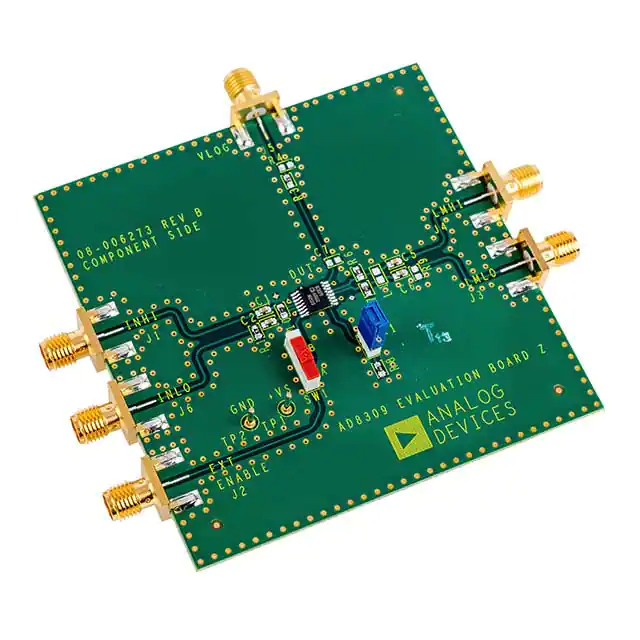
An evaluation board, carefully laid out and tested to demonstrate the specified high speed performance of the AD8309 is
available. Figure 40 shows the schematic of the evaluation board
which fairly closely follows the basic connections schematic
shown in Figure 30. For ordering information, please refer to
the Ordering Guide. Links, switches and component settings for
different setups are described in Table IV.
The AD8309 fundamentally responds to voltage and not to
power. A direct consequence of this characteristic is that input
signals of equal rms power, but differing crest factors, will produce different results at the log amp’s output.
The effect of differing signal waveforms is to shift the effective
value of the log amp’s intercept. Graphically, this looks like a
vertical shift in the log amp’s transfer function. The device’s
logarithmic slope however is not affected. For example, consider
R3
0V
R2
4.7V
+VS
C1
0.01mF
SIG
INHI
C3
0.1mF
R1
0V
2 VPS1
VPS2 15
3 PADL
PADL 14
4 INHI
R5
4.7V
R6
402V
C4
0.1mF
R7
402V
+VS
C5
0.01mF
LMHI 13
LMHI
C7 (OPEN)
5 INLO
LMLO 12
6 PADL
PADL 11
VRSSI
L1
(OPEN)
LMLO
C2
0.01mF
A
EXT
ENABLE
VLOG 16
AD8309
R/L
52.3V
SIG
INLO
1 COM2
R4
(OPEN)
7 COM1
FLTR 10
8 ENBL
LMDR 9
C6
0.01mF
LK1
R8
402V
B
Figure 40. Evaluation Board Schematic
–18–
REV. B
�AD8309
Table IV. Evaluation Board Setup Options
Component
Function
Default Condition
SW1
Device Enable. When in position A, the ENBL pin is connected to +VS and the
AD8309 is in normal operating mode. In position B, the ENBL pin is connected
to an SMA connector labeled Ext Enable. An applied signal can be applied to this
connector to enable/disable the AD8309. If left open, the ENBL pin will float to
ground putting the device in power-down mode.
SW1 = A
R1
This pad is used to ac-couple to ground for single-ended input drive. To drive the
AD8309 differentially, R1 should be removed.
R1 = 0 Ω
R/L, C1, C2
Input Interface. The 52.3 Ω resistor in position R/L along with C1 and C2 create
a high pass input filter whose corner frequency (640 kHz) is equal to 1/(πRC),
where C = C1 = C2 and R is the parallel combination of 52.3 Ω and the AD8309’s
input impedance of 1000 Ω. Alternatively, the 52.3 Ω resistor can be replaced by
an inductor to form an input matching network. See Input Matching Network
section for more details.
R/L= 52.3 Ω
C1 = C2 = 0.01 µF
R3/R4
Slope Adjust. A simple slope adjustment can be implemented by adding a resistive
divider at the VLOG output. R3 and R4, whose sum should be about 1 kΩ, and
never less than 40 Ω (see specs), set the slope according to the equation:
Slope = 20 mV/dB × R4/(R3+R4).
R3 = 0 Ω
R4 = ⬁
L1, C5, C6
Limiter Output Coupling. C5 and C6 ac-couple the limiter’s differential outputs.
By adjusting these values and installing an inductor in L1, an output matching
network can be implemented.
L1 = Open
C5 = 0.01 µF
C6 = 0.01 µF
R8, LK1
Limiter Output Current. With LK2 installed, R8 enables and sets the limiter
output current. The limiter’s output current is set according to the equation
(IOUT = 400 mV/R8). The limiter current can be as high as 10 mA (R8 = 40 Ω).
To disable the limiter (recommended if the limiter is not being used), LK3 should
be removed.
LK1 Installed. R8 = 402 Ω
C7
RSSI Bandwidth Adjust. The addition of C7 will lower the RSSI bandwidth of the
VLOG output according to the equation: fCORNER = 12.7 × 10⁻⁶/(CFILT + 3.5 pF).
C7 = Open
Figure 42. Layout of Power Layer
Figure 41. Layout of Signal Layer
REV. B
–19–
�C3440b–0–8/99
AD8309
Figure 43. Signal Layer Silkscreen
Figure 44. Power Layer Silkscreen
OUTLINE DIMENSIONS
Dimensions shown in inches and (mm).
16-Lead TSSOP
(RU-16)
0.201 (5.10)
0.193 (4.90)
9
0.256 (6.50)
0.246 (6.25)
0.177 (4.50)
0.169 (4.30)
16
1
8
0.0256
SEATING (0.65)
PLANE BSC
0.0433
(1.10)
MAX
0.0118 (0.30)
0.0075 (0.19)
8°
0°
0.0079 (0.20)
0.0035 (0.090)
–20–
PRINTED IN U.S.A.
PIN 1
0.006 (0.15)
0.002 (0.05)
0.028 (0.70)
0.020 (0.50)
REV. B
�


 工商网监
湘ICP备2023018690号
工商网监
湘ICP备2023018690号
