Evaluation Board User Guide
UG-075
One Technology Way • P.O. Box 9106 • Norwood, MA 02062-9106, U.S.A. • Tel: 781.329.4700 • Fax: 781.461.3113 • www.analog.com
AD9516-x, AD9517-x, and AD9518-x Evaluation Board
FEATURES
GENERAL DESCRIPTION
Simple power connection using 6 V wall adapter and
on-board LDO voltage regulators
LDOs are easily bypassed for power measurements
8 ac-coupled differential LVPECL SMA connectors
2 ac-coupled LVPECL differential headers
2 dc-coupled differential LVDS SMA connectors that are
reconfigurable to four CMOS SMA connectors
2 dc-coupled LVDS differential headers that are
reconfigurable to four CMOS connectors
SMA connectors for
2 reference inputs
Charge pump output
Clock distribution input
USB connection to PC
Microsoft Windows-based evaluation software with simple
graphical user interface
On-board PLL loop filter
Easy access to digital I/O and diagnostic signals
via I/O header
Status LEDs for diagnostic signals
The AD9516-x, AD9517-x, and AD9518-x are very low noise
PLL clock synthesizers featuring an integrated VCO, clock
dividers, and up to 14 outputs. The AD9516 features automatic
holdover and a flexible reference input circuit allowing for very
smooth reference clock switching. The AD9516 family also
features the necessary provisions for an external VCXO.
The AD9516 evaluation board is a compact, easy-to-use
platform for evaluating all features of the AD9516. This user
guide covers all six versions of the AD9516 family, as well as
the AD9517 and AD9518 families (hereafter referred to as
AD951x). The AD9516, AD9517, and AD9518 differ only
in package size, and the number of outputs. The evaluation
software main window for the AD9517 and AD9518 reflects
fewer outputs, but the operation is identical for all devices.
Although the Quick Start Guide to the AD9516 PLL section
applies specifically to the AD9516-3, increasing the N (feedback) divider and channel divider increases the VCO frequency
to the allowable frequency range of other AD9516 versions.
For the AD9516-5, which lacks an internal VCO, certain
portions of this document that apply to the internal VCO
(such as VCO calibration) can be ignored.
APPLICATIONS
Clocking of analog-to-digital and digital-to-analog
converters up to 2.9 GHz
Networking and communications line cards
Test and measurement equipment
Wireless base stations, controllers
Clock cleanup/jitter attenuation
Clock distribution
For convenience, detailed information from the AD9516 data
sheet has been included here. Use this user guide in conjunction
with the AD9516, AD9517, and AD9518 data sheets, as well as
additional documentation available at www.analog.com.
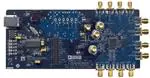
08745-001
AD9516 EVALUATION BOARD
Figure 1.
See the last page for an important warning and disclaimers.
Rev. 0 | Page 1 of 16
�UG-075
Evaluation Board User Guide
TABLE OF CONTENTS
Features .............................................................................................. 1
REFMON, STATUS, and LD Buttons.........................................8
Applications ....................................................................................... 1
Register W/R Box ..........................................................................9
General Description ......................................................................... 1
SYNC, PD (Power Down), and RESET Buttons .......................9
AD9516 Evaluation Board............................................................... 1
Reference (R) Divider Window ...................................................9
Revision History ............................................................................... 2
R and N Delay Window ................................................................9
Evaluation Board Hardware ............................................................ 3
Feedback (N) Divider Window ...................................................9
Power and PC Connections ........................................................ 3
Phase Frequency Detector (PFD) Window ............................ 10
Signal Connections ...................................................................... 3
Charge Pump Window .............................................................. 10
Bypassing the Wall Power Supply............................................... 3
VCO Calibration Window ........................................................ 10
Bypassing the PLL (Clock Distribution Only) ............................. 3
Channel Divider Window ......................................................... 11
Using an External VCXO ............................................................ 3
LVPECL Output Driver Window ............................................. 11
Evaluation Board Software .............................................................. 4
LVDS/CMOS Output Driver Window .................................... 12
Software Installation .................................................................... 4
LVDS/CMOS Output Delay Window ..................................... 12
Running the Software .................................................................. 4
Debug Window ........................................................................... 12
Quick Start Guide to the AD9516 PLL .......................................... 5
Evaluation Software Menu Items.................................................. 13
Evaluation Software Components .................................................. 7
Menu Bar ..................................................................................... 13
Main Window ............................................................................... 7
AD9516 PLL Loop Filter ............................................................... 14
PLL Reference Input Window .................................................... 8
Loop Filter for Clock Cleanup .................................................. 15
PLL Configuration Window ....................................................... 8
ESD Caution................................................................................ 16
REVISION HISTORY
1/10—Revision 0: Initial Version
Rev. 0 | Page 2 of 16
�Evaluation Board User Guide
UG-075
EVALUATION BOARD HARDWARE
The following instructions are for setting up the physical
connections to the AD951x evaluation board.
SIGNAL CONNECTIONS
When connecting the evaluation board to a PC for the first
time, the user must install the evaluation software prior to
connecting the evaluation board.
1.
To connect signals, use the following steps:
POWER AND PC CONNECTIONS
2.
Use the following steps to connect the AD951x evaluation
board to its power supply and lab equipment.
1.
2.
3.
Install the AD951x evaluation software. Administrative
privileges are required for installation. The 64-bit versions
of Windows® are not supported.
Connect the wall power supply to the main power
connector labeled P2. The following five LEDs should
be on: CR1 (USBSTAT), CR7 (VS), CR8 (VS-CP), CR9
(VS_USB), and CR10 (VS_LVPECL).
Connect the USB cables to the evaluation board and
the computer. The red LED labeled CR2 (VBUS) on
the AD951x evaluation board should illuminate and
the CR1 (USBSTAT) LED should start blinking.
4. If the Found New Hardware Wizard window
automatically appears when the evaluation board is
connected, select Install the software automatically
and click Next.
The Found New Hardware Wizard window may appear
twice, and a system restart may be required.
Refer to the Evaluation Board Software section for details
on running the AD951x evaluation board software.
If the USBSTAT LED is not blinking, ensure that:
•
•
•
Jumpers are installed on Position S1 and Position S2.
The jumper on S4 is across the center pin and the
minus symbol.
The USB port on the PC is operational and that the USB
cable is not damaged.
3.
Connect a signal generator to the J10 SMA connector. By
default, the reference inputs on this evaluation board are
ac-coupled and terminated 50 Ω to ground. An amplitude
setting of 0 dBm to 6 dBm is fine.
If the user wants to connect a signal to REF2, connect that
signal to the J13 SMA connector. DC-coupling is recommended in applications requiring automatic hitless reference
switching. There is a possibility that the device receive
buffer can chatter when an ac-coupled clock stops toggling.
Connect an oscilloscope, spectrum analyzer, or other lab
equipment to any of the J0 to J9 SMA connectors on the
right side of the board.
OUT0 through OUT5 are ac-coupled LVPECLs. OUT8 and
OUT9 are dc-coupled and have no output termination. These
allow the user to evaluate the AD951x output driver in either
LVDS or CMOS mode.
BYPASSING THE WALL POWER SUPPLY
To bypass the wall power supply, remove the following
ferrite beads (on the backside of the board): F7, F4, F2, and
F6. Connect a bench power supply to TB1 on the evaluation
board. This is useful for making AD951x power consumption
measurements.
BYPASSING THE PLL (CLOCK DISTRIBUTION ONLY)
To bypass the PLL, connect a signal generator to the
SMA connector labeled CLK. By default, this connection
is ac-coupled to the CLK pin and terminated with a 50 Ω
resistor to ground. Refer to the Evaluation Software
Components section for details on running the AD951x
evaluation board software.
USING AN EXTERNAL VCXO
To use an external VCXO, use the following steps.
1.
2.
3.
Rev. 0 | Page 3 of 16
Install a 0 Ω resistor at R9 and remove R8.
Connect a loop filter and external VCO/VCXO input to J12.
Connect the external VCO/VCXO output to the J11 SMA
connector (CLK input).
�UG-075
Evaluation Board User Guide
EVALUATION BOARD SOFTWARE
Use the following instructions to set up the AD951x evaluation
board software.
you to load the evaluation board with the evaluation software
settings or read the evaluation board settings into the software.
SOFTWARE INSTALLATION
2.
3.
The evaluation software and documentation can be
downloaded from www.analog.com.
If the software was downloaded, skip to Step 3.If installing
from the CD, insert the AD951x evaluation software CD.
Double-click My Computer and then double-click the
AD9516_17_18EV CD icon. A window opens showing the
contents of the CD divided into four sections: Datasheet,
Layout, Schematic, and Software. The file named
readme.txt contains a description of the CD contents as
well as any additional instructions or information. Doubleclick the Software folder.
Double-click AD9516_17_18Eval_Setup1.1.0.exe. (Note
that the website may have a version newer than Version
1.1.0.) Follow the installation instructions. The default
location for installation of the evaluation software is:
C:\Program Files\Analog Devices\AD9516 Eval Software\.
RUNNING THE SOFTWARE
Power up and connect the evaluation board to the PC.
See Evaluation Board Hardware section for details on the
various connectors on the evaluation board.
1.
2.
Double-click AD9516_17_18 Eval Software to run the
AD951x evaluation software. Depending on whether the
evaluation board was found by the software, either light
blue text appears in a pop-up window, indicating that the
evaluation board was found, or red text appears, indicating
that the evaluation board was not found.
If the evaluation board is found, click anywhere in the popup window with the Evaluation Software Ready message,
and the main window for the software appears. Proceed to
the Evaluation Software Components section for details
about running the software.
If the evaluation board is not found, a dialog box appears
allowing you to select which AD951x evaluation board is
connected while the software runs in standalone mode.
See the Evaluation Board Hardware section for information on
connecting the evaluation board.
Figure 2. SYNC Evaluation Software Window
If the evaluation board was not automatically detected when it
was connected, you can also select the Select Evaluation Board
option from the I/O menu (see Figure 24), and select Ezssp-0,
Ezssp-1, or Ezssp-2.
08745-003
1.
08745-002
Do not connect the evaluation board until the software
installation is complete.
Figure 3. Select USB Device Window
See the Evaluation Software Components section for a
description of the evaluation software features, or the Quick
Start Guide to the AD9516 PLL section for details on the
individual blocks of the AD951x.
If the evaluation board is connected while the evaluation
software is running, the window in Figure 2 appears to prompt
Rev. 0 | Page 4 of 16
�Evaluation Board User Guide
UG-075
QUICK START GUIDE TO THE AD9516 PLL
When the evaluation software is installed, the evaluation board
is connected, and the software is loaded, use the following steps
to configure and lock the PLL. These steps assume that the input
signal is present, the evaluation board has not been modified,
and that the PLL loop filter is suitable for the user’s application.
This quick start guide covers only simple PLL operation to
start the PLL. See the AD9516 data sheet and Evaluation
Software Components section for a detailed explanation
of the various AD9516 features.
The following case is an example for the AD9516-3 using the
values in Table 1.
Table 1.
3.
4.
Turn the PLL on by selecting Normal Op from the PLL
MODE box found at the top of the main window (see
Figure 8).
Enter the intended reference input frequency (in
megahertz) in the REF 1 (MHz) box at the upper left
corner of the main window.
Click the triangular buffer symbol immediately to the right
of the input reference frequency (see Figure 4) boxes to load
the Reference Input Control window shown in Figure 5.
Turn the REF1 reference input buffer on by selecting the
Enable REF1 check box, and then clicking OK.
5.
When the window closes, the WRITE button under the
REGISTER W/R section in the main window blinks red.
This indicates there are settings that have not been loaded
to the AD9516 evaluation board. Click the blinking red
WRITE button to load these settings to the evaluation
board.
Select the VCO as the input to the clock distribution
circuitry by clicking the mux symbol that is located
immediately to the right of the VCO (MHz) box (see
Figure 6).
08745-023
2.
Figure 5. Reference Input Control Window
Figure 6. Buffer Symbol
When the VCO is selected, the border of the VCO (MHz)
box changes from gray to black. The current VCO
frequency is shown in the VCO (MHz) box.
08745-006
1.
Value
20 MHz on REF1
200 MHz on OUT1
2
10 MHz
200
2000 MHz
2
5
08745-004
Parameter
Input Frequency
Output Frequency
Reference Divider
Phase Detector Frequency
Feedback Divider
VCO Frequency
VCO Divider
Channel Divider
Figure 4. Buffer Symbol
Rev. 0 | Page 5 of 16
�UG-075
Program the R (reference) divider by clicking the
R DIVIDER box at the top of the main window. Set
the desired value and click OK (see Figure 12).
7. Program the N (feedback) divider by clicking the
N DIVIDER box at top of the main window. Set the
desired value and click OK. For the example, N = 200
can use 8/9 dual modulus mode with A = 0 and B = 25.
8. Set the charge pump current by clicking the CHARGE
PUMP box in the upper right corner of the main window,
and then click OK.
9. Note that if the desired configuration has the phase
detector frequency above 50 MHz, an antibacklash pulse
width of 1.3 ns may work better. This setting is accessed by
clicking the PFD button to the left of the CHARGE PUMP
box. However, this setting normally does not need to be
modified.
10. Set the VCO divider by clicking the green VCO box in the
center of the main window, immediately to the left of the
Cal VCO button.
11. Power down unused drivers, click the numbered triangular
symbol on the right side of the main window (see Figure 7),
select 2 - Safe Power Down, and click OK (see Figure 20).
08745-024
6.
Evaluation Board User Guide
Figure 7. Driver Symbol
12. Set the channel dividers by clicking DIVIDER 0 through
DIVIDER 4 and enter the divider ratio.
13. Click the flashing red WRITE button under the
REGISTER W/R section. This loads the desired settings
to the AD951x evaluation board,
14. Click the blinking yellow Cal VCO button to load the
VCO calibration window. The default VCO divide ratio
(16) works for all applications. Click the Cal VCO button
in the Calibrate VCO window to begin calibration (see
Figure 17). The PLL should now be locked and the LD
(lock detect) LED on the left side of the board should be on.
Rev. 0 | Page 6 of 16
�Evaluation Board User Guide
UG-075
EVALUATION SOFTWARE COMPONENTS
08745-005
MAIN WINDOW
Figure 8. Evaluation Software Main Window
The AD951x evaluation software is composed of subsections
that correspond to the major functional blocks of the AD951x.
These subsections are listed in the following sections and each
of these has its own window. From the main window, each
functional block can be accessed by clicking that block in the
main window.
When a subwindow closes after clicking OK, the WRITE box
on the main window (under the REGISTER W/R section) may
blink red. This indicates that there are settings that have not
been loaded to the AD951x evaluation board. Clicking the
blinking red WRITE button loads these settings to the
evaluation board.
Rev. 0 | Page 7 of 16
�UG-075
Evaluation Board User Guide
PLL REFERENCE INPUT WINDOW
PLL CONFIGURATION WINDOW
The Reference Input Control window is shown in Figure 10
and is accessed by clicking either of the triangular buffer symbols
immediately to the right of the REF 1 (MHz) and REF 2 (MHz)
input reference frequency boxes (see Figure 9).
The PLL Configuration window shown in Figure 11 is opened
by clicking the Config PLL button on the main screen. This
window has three sections: SyncB Counter Reset Mode,
ReadBack Registers, and Settings.
The SyncB Counter Reset Mode section indicates whether the
R, A, and B counters are reset when the SYNC pin is activated, and
controls R0x019[7:6]. See the AD951x data sheet for more
details.
08745-006
The ReadBack Registers section allows you to see the current
value of the read-only PLL status register (Address 0x01F). This
function is very useful for ensuring that the AD951x VCO has
finished VCO calibration, and that the PLL is locked.
Figure 9. Buffer Symbol
The Settings section controls the various PLL settings such as holdover. The AD951x data sheet describes these functions in detail.
08745-007
Note that the automatic holdover feature should not be enabled
during VCO calibration.
08745-008
Figure 10. Reference Input Control Window
This window is used to enable the PLL reference inputs, which
are powered down by default.
Select Enable REF 1, or Enable REF 2, or both to enable the
appropriate reference input, and click OK when finished. If a
differential input is used, select the Use Differential Ref Mode
(Unchecked = Single-Ended Mode) check box. Note that this
mode should not be used simultaneously with Enable REF 1
or Enable REF 2.
The remaining four check boxes control the reference switchover modes. If Disable Switchover De-Glitch is activated, the
AD951x maintains the phase relationship between the active
input and PLL output during a reference switchover. Otherwise,
the AD951x minimizes the phase disturbance at the output
during a reference switchover.
Figure 11. PLL Configuration Window
REFMON, STATUS, AND LD BUTTONS
These three blue buttons (REFMON, STATUS, and LD) allow
you to select which signals appear at the REFMON, STATUS,
and LD pins at Connector P1. Connector P1 is located in the
center of the evaluation board. The pins in the left column
of Connector P1 are ground pins, and the ones in the right
column are signal pins.
There are many useful diagnostic signals available at these
pins. The R divider output is particularly useful. In the example
used in the Quick Start Guide to the AD9516 PLL section, the
80 kHz signal is visible on the STATUS pin to ensure that the
reference inputs and R divider are working properly.
Dynamic signals (such as the R divider output) are primarily
intended for diagnostics. These diagnostic signals may adversely
affect PLL performance in critical applications if left on in
normal operation.
Rev. 0 | Page 8 of 16
�Evaluation Board User Guide
UG-075
REGISTER W/R BOX
R AND N DELAY WINDOW
The REGISTER W/R (write/read) box has four buttons and
three check boxes.
The AD951x features two delay circuits (one on the reference
divider path, and one on the feedback divider path) that allow
the user to control the static phase offset between the reference
input and the PLL output. The R Path Delay window shown in
Figure 13 is accessed by clicking the R DELAY button on the
main screen. The R DELAY box is identical to the N DELAY
box. These delay settings allow you to vary the static phase
offset of the PLL.
The WRITE button transfers the values stored in the evaluation
software to the evaluation board. It blinks red when register
values have changed.
The READ button transfers the values stored in the evaluation
board to the evaluation software.
The UPDATE button issues an I/O update command by writing
0x01 to Register 0x232.
Selecting the All check box transfers all of the registers when
the WRITE button is clicked. When this check box is cleared,
only the registers whose value has changed are written.
Selecting the Auto check box adjacent to the WRITE box
forces the evaluation software to write the register changes
to the evaluation board automatically when they occur.
08745-010
Selecting the Auto check box adjacent to the UPDATE box
forces the evaluation software to issue an I/O update command
whenever registers are written to the AD951x. It is checked by
default.
SYNC, PD (POWER DOWN), AND RESET BUTTONS
Figure 13. R Path Delay Window
The SYNC, PD, and RESET buttons allow you to control the
SYNC, PD, and RESET pins on the AD951x.
FEEDBACK (N) DIVIDER WINDOW
Each button has three options: Strobe, Latch, and Release.
Strobe activates the pin, and then releases it. Latch holds
the pin active until the Release command is issued.
The reference divider window shown in Figure 14 is accessed by
clicking the N DIVIDER box on the main screen. If this box is
colored gray, the PLL is off. To turn the PLL on, click the PLL
MODE box at the top of the main screen, and select Norm Op.
REFERENCE (R) DIVIDER WINDOW
The R Divider window shown in Figure 12 is accessed by
clicking the R DIVIDER box on the main window. It allows
you to set the reference divider. If this box is colored gray, the
PLL is off. To turn the PLL on, click the PLL MODE box at
the top of the main window, and select Norm Op.
08745-011
The R Divider window has a check box for holding the
R divider in reset. When the R divider is held in reset, the
PLL loop is opened. Therefore, this feature is seldom used.
08745-009
Figure 14. N Divider Window
Figure 12. R Divider Window
The various modes of the N divider are described in detail in
the AD951x data sheet. For most applications, the 8/9 or 16/17
dual modulus modes are used. For applications requiring a
divider value larger than 131,119, the 32/33 mode is provided.
Different applications require different settings, and you can
experiment with the different settings.
Rev. 0 | Page 9 of 16
�UG-075
Evaluation Board User Guide
The evaluation software has internal checking to ensure that
invalid settings are not programmed. For example, the B
counter must always be larger than the A counter. Another
restriction is that 8/9 dual modulus mode cannot be used for
VCO frequencies greater than 2400 MHz. In cases where a
feedback divider restriction cannot be resolved, you may need
to adjust the R (reference) divider to allow a different feedback
divider value. For example, it is not possible to use the internal
VCO, and a feedback divider of 30. However, the R divider can
be doubled, which allows a feedback divider of 60.
CHARGE PUMP WINDOW
The Charge Pump Setup window shown in Figure 16 is accessed
by clicking the CHARGE PUMP box on the main screen.
The feedback divider window has a check box for holding the
N divider in reset. When the N divider is held in reset, the PLL
loop is open. Therefore, this feature is seldom used.
PHASE FREQUENCY DETECTOR (PFD) WINDOW
08745-013
The Phase Frequency Detector (PFD) window shown in
Figure 15 is accessed by clicking the PFD box on the main
window.
Figure 16. Charge Pump Setup Window
This window is most often used to vary the charge pump
current.
The window also has a check box for setting the charge pump
voltage to VCP/2, which is very useful for debugging the PLL and
isolating the output driver section of the AD951x from the PLL
section.
VCO CALIBRATION WINDOW
08745-012
The Calibrate VCO window shown in Figure 17 is accessed by
clicking the Cal VCO button on the main window.
Figure 15. Phase Frequency Detector Window
The features accessible in this window are described in detail in
the AD951x data sheet. The most commonly used settings are
the Anti-Backlash Pulse Width and the Lock Detect Counter.
Setting the lock detect counter to values greater then 5 PFD
cycles can be useful in applications where the loop bandwidth
is low and the lock detect counter chatters during acquisition.
08745-014
For phase detector frequencies greater than 50 MHz, the PLL
may work better with the 1.3 ns antibacklash pulse width setting.
Figure 17. Calibrate VCO Window
A valid reference input signal must be present to complete VCO
calibration, and the VCO must be recalibrated any time the
VCO frequency changes by more than 40 MHz.
A VCO divider of 16 is suitable for all applications. However,
for applications where the phase detector frequency is


 工商网监
湘ICP备2023018690号
工商网监
湘ICP备2023018690号
