Quad Input Multiservice Line Card Adaptive
Clock Translator with Frame Sync
AD9558
Data Sheet
FEATURES
Pin program function for easy frequency translation
configuration
Software controlled power-down
64-lead, 9 mm × 9 mm, LFCSP package
Supports GR-1244 Stratum 3 stability in holdover mode
Supports smooth reference switchover with virtually
no disturbance on output phase
Supports Telcordia GR-253 jitter generation, transfer, and
tolerance for SONET/SDH up to OC-192 systems
Supports ITU-T G.8262 synchronous Ethernet slave clocks
Supports ITU-T G.823, G.824, G.825, and G.8261
Auto/manual holdover and reference switchover
4 reference inputs (single-ended or differential)
Input reference frequencies: 2 kHz to 1250 MHz
Reference validation and frequency monitoring (1 ppm)
Programmable input reference switchover priority
20-bit programmable input reference divider
6 pairs of clock output pins with each pair configurable as
a single differential LVDS/HSTL output or as 2 single-ended
CMOS outputs
Output frequencies: 352 Hz to 1250 MHz
Programmable 17-bit integer and 23-bit fractional
feedback divider in digital PLL
Programmable digital loop filter covering loop bandwidths
from 0.1 Hz to 5 kHz (2 kHz maximum for 705 MHz
The reference input divide-by-2 block must be
engaged for fIN > 705 MHz
Minimum limit imposed for jitter performance
Internally generated
Minimum differential voltage across pins is required to
ensure switching between logic levels; instantaneous
voltage on either pin must not exceed the supply rails
mV
mV
mV
mV
kΩ
pF
390
640
0.002
40
Test Conditions/Comments
V
V
V
kΩ
pF
ns
ns
Rev. C | Page 8 of 105
Minimum limit imposed for jitter performance
�Data Sheet
AD9558
REFERENCE MONITORS
Table 8.
Parameter
REFERENCE MONITORS
Reference Monitor
Loss of Reference Detection Time
Min
Frequency Out-of-Range Limits
1
WRITE:
REGISTER 0x0005 = 0x01
START TIMEOUT CLOCK:
TIME = 0
REGISTER PROGRAMMING OVERVIEW
NO
DISTRIBUTION
SYNCHRONIZATION
OPERATION
YES
WRITE REGISTER 0x0A02 = 0x02
4.
WRITE REGISTER 0x0005 = 0x01
WRITE REGISTER 0x0A02 = 0x00
END
09758-233
WRITE REGISTER 0x0005 = 0x01
5.
Figure 37. AD9558 APLL Initialization Subprocess Flowchart
Rev. C | Page 28 of 105
Set the system clock PLL input type and divider values.
Set the system clock period.
It is essential to program the system clock period because
many of the AD9558 subsystems rely on this value.
Set the system clock stability timer.
It is highly recommended that the system clock stability
timer be programmed. This is especially important when
using the system clock multiplier and also applies when
using an external system clock source, especially if the
external source is not expected to be completely stable
when power is applied to the AD9558. The system clock
stability timer specifies the amount of time that the system
clock PLL must be locked before the device declares that
the system clock is stable. The default value is 50 ms.
Program the free run tuning word.
The free run frequency of the digital PLL (DPLL)
determines the frequency appearing at the APLL input
when free run mode is selected. The free run tuning word
is at Register 0x0300 to Register 0x0303. The correct free
run frequency is required for the APLL to calibrate and
lock correctly.
Set user free run mode (Register 0x0A01, Bit 5 = 1b).
�Data Sheet
AD9558
Initialize and Calibrate the Output PLL (APLL)
Generate the Output Clock
The registers controlling the APLL are at Register 0x0400
to Register 0x0408. This low noise, integer-N PLL multiplies
the DPLL output (which is usually 175 MHz to 200 MHz) to a
frequency in the 3.35 GHz to 4.05 GHz range. After the system
clock is configured and the free run tuning word is set in
Register 0x0300 to Register 0x0303, the user can set the manual
APLL VCO calibration bit (Register 0x0405, Bit 0) and issue an
I/O update (Register 0x0005, Bit 0). This process performs the
APLL VCO calibration. VCO calibration ensures that, at the time
of calibration, the dc control voltage of the APLL VCO is centered
in the middle of its operating range. It is important to remember
the following points when calibrating the APLL VCO:
If Register 0x0500, Bits[1:0] is programmed for automatic clock
distribution synchronization via the DPLL phase or frequency
lock, the synthesized output signal appears at the clock distribution
outputs. Otherwise, set and then clear the soft sync clock
distribution bit (Register 0x0A02, Bit 1), or use a multifunction
pin input (if programmed for use) to generate a clock
distribution sync pulse, which causes the synthesized output
signal to appear at the clock distribution outputs.
•
•
•
•
•
The system clock must be stable.
The APLL VCO must have the correct frequency from the
30-bit digitally controlled oscillator (DCO) during
calibration.
The APLL VCO must be recalibrated any time the APLL
frequency changes.
APLL VCO calibration occurs on the low-to-high transition
of the manual APLL VCO calibration bit, and this bit is not
autoclearing. Therefore, this bit must be cleared (and an I/O
update issued) before another APLL calibration is started.
The best way to monitor successful APLL calibration is to
monitor Bit 2 in Register 0x0D01 (APLL lock).
Program the Clock Distribution Outputs
The APLL output goes to the clock distribution block. The
clock distribution parameters reside in Register 0x0500 to
Register 0x0515. They include the following:
•
•
•
•
•
Output power-down control
Output enable (disabled by default)
Output synchronization
Output mode control
Output divider functionality
Program the Multifunction Pins (Optional)
This step is required only if the user intends to use any of the
multifunction pins for status or control. The multifunction pin
parameters are in Register 0x0200 to Register 0x0208.
Program the IRQ Functionality (Optional)
This step is required only if the user intends to use the IRQ feature.
The IRQ monitor registers are in Register 0x0D02 to
Register 0x0D09. If the desired bits in the IRQ mask registers at
Register 0x020A to Register 0x020F are set high, the appropriate
IRQ monitor bit at Register 0x0D02 to Register 0x0D07 is set
high when the indicated event occurs.
Individual IRQ events are cleared by using the IRQ clearing the
registers at Register 0x0A04 to Register 0x0A09, or by setting
the clear all IRQs bit (Register 0x0A03, Bit 1) to 1b.
The default values of the IRQ mask registers are such that
interrupts are not generated. The IRQ pin mode default is
open-drain NMOS.
Program the Watchdog Timer (Optional)
This step is required only if the user intends to use the watchdog
timer. The watchdog timer control is in Register 0x0210 and
Register 0x0211 and is disabled by default.
The watchdog timer is useful for generating an IRQ after a fixed
amount of time. The timer is reset by setting the clear watchdog
timer bit (Register 0x0A03, Bit 0) to 1b.
See the Clock Distribution section for more information.
Rev. C | Page 29 of 105
�AD9558
Data Sheet
Program the Digital Phase-Locked Loop (DPLL)
Program the Reference Profiles
The DPLL parameters reside in Register 0x0300 to
Register 0x032E. They include the following:
The reference profile parameters reside in Register 0x0700 to
Register 0x07E6. The AD9558 evaluation software contains a
wizard that calculates these values based on the user input
frequency. See the Reference Profiles section for details on
programming these functions. They include the following:
•
•
•
•
•
Free run frequency
DPLL pull-in range limits
DPLL closed-loop phase offset
Phase slew control (for hitless reference switching)
Tuning word history control (for holdover operation)
Program the Reference Inputs
The reference input parameters reside in Register 0x0600 to
Register 0x0602. See the Reference Clock Input section for
details on programming these functions. They include the
following:
•
•
•
Reference power-down
Reference logic family
Reference priority
•
•
•
•
•
•
•
•
Reference period
Reference period tolerance
Reference validation timer
Selection of high phase margin loop filter coefficients
DPLL loop bandwidth
Reference prescaler (R divider)
Feedback dividers (N1, N2, N3, FRAC1, and MOD1)
Phase and frequency lock detector controls
Generate the Reference Acquisition
After the registers are programmed, the user can clear the user
free run bit (Register 0x0A01, Bit 5) and issue an I/O update,
using Register 0x0005, Bit 0, to invoke all of the register settings
that are programmed up to this point.
After the registers are programmed, the DPLL locks to the first
available valid reference that has the highest priority.
Rev. C | Page 30 of 105
�Data Sheet
AD9558
SPI/I2C
SERIAL PORT
EEPROM
REFA
REFA
÷2
REFB
REFB
÷2
REFC
REFC
÷2
REFD
REFD
÷2
XO OR XTAL
PINCONTROL
REGISTER
SPACE
M0 M1 M2 M3 M4 M5 M6 M7 IRQ
ROM
AND
FSM
R DIVIDER
(20-BIT)
17-BIT
INTEGER
FRAC1/
÷N1
MOD1
÷2
×2
RF
DIVIDER 1
÷3 TO ÷11
DIGITAL
LOOP
FILTER
FRAME SYNC
MODE ONLY
÷M1
×2
TUNING
WORD
CLAMP
AND
HISTORY
÷M2
÷M3
FRAME SYNC PULSE
OUT1
OUT1
OUT3
OUT3
OUT4
OUT4
÷M3b
×2
OUT5
OUT5
÷N2
OUTPUT PLL (APLL)
REF MONITORING
AUTOMATIC
SWITCHING
OUT0
OUT2
30-BIT
NCO
DIGITAL PLL (DPLL)
OUT0
OUT2
MAX 1.25GHz
RF
DIVIDER 2
÷3 TO ÷11
FREE RUN
TW
DPFD
÷M0 TO ÷M3b ARE
10-BIT INTEGER
DIVIDERS
÷M0
MULTIFUNCTION I/O PINS
(CONTROL AND STATUS
READBACK)
SYSTEM
PFD/CP ÷N3
CLOCK
MULTIPLIER
LF
23-BIT/23-BIT
RESOLUTION
AD9558
XO OR REF FREQUENCIES
10MHz TO 600MHz
XTAL: 10MHz TO 50MHz
PFD/CP
2kHz TO 8kHz FRAME SYNC SIGNAL
APLL
STATUS
LF
360kHz TO 1.25GHz
2kHz TO 1.25GHz
SPI/I2C
RESET
352Hz
TO 1.25GHz
SYNC
3.35GHz
TO
4.05GHz
LF_VCO2
09758-135
THEORY OF OPERATION
Figure 38. Detailed Block Diagram
OVERVIEW
The AD9558 provides clocking outputs that are directly related
in phase and frequency to the selected (active) reference, but
with jitter characteristics that are governed by the system clock,
the DCO, and the analog integer-N PLL (APLL). The AD9558
supports up to four reference inputs and input frequencies ranging
from 2 kHz to 1250 MHz. The core of this product is a digital
phase-locked loop (DPLL). The DPLL has a programmable
digital loop filter that greatly reduces jitter that is transferred
from the active reference to the output. The AD9558 supports
both manual and automatic holdover. While in holdover, the
AD9558 continues to provide an output as long as the system
clock is present. The holdover output frequency is a time average
of the output frequency history just prior to the transition to the
holdover condition. The device offers manual and automatic
reference switchover capability if the active reference is degraded
or fails completely. The AD9558 also has adaptive clocking
capability that allows the DPLL divider ratios to be changed
while the DPLL is locked.
The AD9558 has a system clock multiplier, a DPLL, and an APLL.
The input signal goes first to the DPLL, which performs the jitter
cleaning and most of the frequency translation. The DPLL
features a 30-bit digitally controlled oscillator (DCO) output
that generates a signal in the 175 MHz to 200 MHz range. The
DPLL output goes to an APLL, which multiplies the signal up to
the 3.35 GHz to 4.05 GHz range. That signal is then sent to the
clock distribution section, which has two divide-by-3 to divideby-11 RF dividers that are cascaded with 10-bit integer (divideby-1 to divide-by-1024) channel dividers.
The XOA and XOB pins provide the input for the system clock.
These pins accept a reference clock in the 10 MHz to 600 MHz
range, or a 10 MHz to 50 MHz crystal connected directly across
the XOA and XOB pins. The system clock provides the clocks to
the frequency monitors, the DPLL, and internal switching logic.
The AD9558 has six output drivers, arranged into four
channels. Each channel has a dedicated 10-bit programmable
post divider. Channel 0 and Channel 3 have one driver each,
and Channel 1 and Channel 2 have two drivers each. Each
driver is programmable either as a single differential or dual
single-ended CMOS output. The clock distribution section
operates at up to 1250 MHz.
In differential mode, the output drivers run on a 1.8 V power
supply to offer very high performance with minimal power
consumption. There are two differential modes: LVDS and
1.8 V HSTL. In 1.8 V HSTL mode, the voltage swing is
compatible with LVPECL. If LVPECL signal levels are required,
the designer can ac couple the AD9558 output and use
Thevenin-equivalent termination at the destination to drive
the LVPECL inputs.
In single-ended mode, each differential output driver can
operate as two single-ended CMOS outputs. OUT0 and OUT5
support either 1.8 V or 3.3 V CMOS operation. OUT1 through
OUT4 support only 1.8 V operation.
Note that the APLL is also referred to as the output PLL
elsewhere in this data sheet.
Rev. C | Page 31 of 105
�AD9558
Data Sheet
REFERENCE CLOCK INPUTS
Reference Validation Timer
Four pairs of pins provide access to the reference clock receivers.
To accommodate input signals with slow rising and falling edges,
both the differential and single-ended input receivers employ
hysteresis. Hysteresis also ensures that a disconnected or
floating input does not cause the receiver to oscillate.
Each reference input has a dedicated validation timer. The
validation timer establishes the amount of time that a previously
faulted reference must remain unfaulted before the AD9558
declares it valid. The timeout period of the validation timer is
programmable via a 16-bit register. The 16-bit number stored
in the validation register represents units of milliseconds (ms),
which yields a maximum timeout period of 65,535 ms.
When configured for differential operation, the input receivers
accommodate either ac- or dc-coupled input signals. The input
receivers are capable of accepting dc-coupled LVDS and 2.5 V
and 3.3 V LVPECL signals. The receiver is internally dc biased
to handle ac-coupled operation, but there is no internal 50 Ω or
100 Ω termination.
When configured for single-ended operation, the input
receivers exhibit a pull-down load of 45 kΩ (typical). Three
user-programmable threshold voltage ranges are available for
each single-ended receiver.
REFERENCE MONITORS
The accuracy of the input reference monitors depends on a
known and accurate system clock period. Therefore, the
functioning of the reference monitors is not operable until the
system clock is stable.
Reference Period Monitor
Each reference input has a dedicated monitor that repeatedly
measures the reference period. The AD9558 uses the reference
period measurements to determine the validity of the reference
based on a set of user-provided parameters in the profile
register area of the register map.
The monitor works by comparing the measured period of a
particular reference input with the parameters stored in the
profile register assigned to that same reference input. The
parameters include the reference period, an inner tolerance,
and an outer tolerance. A 40-bit number defines the reference
period in units of femtoseconds (fs). The 40-bit range allows a
reference period entry of up to 1.1 ms. A 20-bit number defines
the inner and outer tolerances. The value stored in the register
is the reciprocal of the tolerance specification. For example, a
tolerance specification of 50 ppm yields a register value of
1/(50 ppm) = 1/0.000050 = 20,000 (0x04E20).
The use of two tolerance values provides hysteresis for the
monitor decision logic. The inner tolerance applies to a
previously faulted reference and specifies the largest period
tolerance that a previously faulted reference can exhibit before it
qualifies as nonfaulted. The outer tolerance applies to an already
nonfaulted reference. It specifies the largest period tolerance
that a nonfaulted reference can exhibit before being faulted.
To produce decision hysteresis, the inner tolerance must be less
than the outer tolerance. That is, a faulted reference must meet
tighter requirements to become nonfaulted than a nonfaulted
reference must meet to become faulted.
It is possible to disable the validation timer by programming the
validation timer to 0b. With the validation timer disabled, the
user must validate a reference manually via the manual reference
validation override controls register (Address 0x0A0B).
Reference Validation Override Control
The user also has the ability to override the reference validation
logic and can either force an invalid reference to be treated as valid,
or force a valid reference to be treated as an invalid reference.
These controls are in Register 0x0A0B to Register 0x0A0D.
REFERENCE PROFILES
The AD9558 has an independent profile for each reference input.
A profile consists of a set of device parameters such as the R divider
and N divider, among others. The profiles allow the user to
prescribe the specific device functionality that takes effect when
one of the input references becomes the active reference.
The AD9558 evaluation software includes a frequency planning
wizard that can configure the profile parameters, given the
input and output frequencies.
Do not change a profile that is currently in use because
unpredictable behavior may result. The user can either select
free run or holdover mode or invalidate the reference input
prior to changing it.
REFERENCE SWITCHOVER
An attractive feature of the AD9558 is its versatile reference
switchover capability. The flexibility of the reference switchover
functionality resides in a sophisticated prioritization algorithm
that is coupled with register-based controls. This scheme
provides the user with maximum control over the state machine
that handles reference switchover.
The main reference switchover control resides in the loop
mode register (Address 0x0A01). The REF switchover mode
bits (Register 0x0A01, Bits[4:2]) allow the user to select one of
the five operating modes of the reference switchover state machine,
as follows:
•
•
•
•
•
Rev. C | Page 32 of 105
Automatic revertive mode
Automatic nonrevertive mode
Manual with automatic fallback mode
Manual with holdover mode
Full manual mode (without automatic holdover)
�Data Sheet
AD9558
In the automatic modes, a fully automatic priority-based algorithm
selects which reference is the active reference. When programmed
for an automatic mode, the device chooses the highest priority
valid reference. When both references have the same priority,
REFA gets preference over REFB. However, the reference position
is used only as a tie-breaker and does not initiate a reference switch.
The following list gives an overview of the five operating modes:
•
•
•
•
•
Automatic revertive mode. The device selects the highest
priority valid reference and switches to a higher priority
reference if it becomes available, even if the reference in use
is still valid. In this mode, the user reference is ignored.
Automatic non-revertive mode. The device stays with the
currently selected reference as long as it is valid, even if
a higher priority reference becomes available. The user
reference is ignored in this mode.
Manual with automatic fallback mode. The device uses the
user reference for as long as it is valid. If it becomes invalid,
the reference input with the highest priority is chosen in
accordance with the priority-based algorithm.
Manual with holdover mode. The user reference is the
active reference until it becomes invalid. At that point,
the device automatically goes into holdover.
Manual mode without holdover. The user reference is the
active reference, regardless of whether or not it is valid.
The user also has the option to force the device directly into
holdover or free run operation via the user holdover and user
free run bits. In free run mode, the free run frequency tuning
word register defines the free run output frequency. In holdover
mode, the output frequency depends on the holdover control
settings (see the Holdover section).
Phase Build-Out Reference Switching
The AD9558 supports phase build-out reference switching,
which is the term given to a reference switchover that
completely masks any phase difference between the previous
reference and the new reference. That is, there is virtually no
phase change detectable at the output when a phase build-out
switchover occurs.
TUNING
WORD
CLAMP
AND
HISTORY
17-BIT
23-BIT/23-BIT
INTEGER RESOLUTION
A TDC samples the output of the R-divider. The TDC/PFD
produces a time series of digital words and delivers them to the
digital loop filter. The digital loop filter offers the following
advantages:
•
•
•
•
Determination of the filter response by numeric
coefficients rather than by discrete component values
The absence of analog components (R/L/C), which
eliminates tolerance variations due to aging
The absence of thermal noise associated with analog
components
The absence of control node leakage current associated
with analog components (a source of reference feedthrough spurs in the output spectrum of a traditional
analog PLL)
The digital loop filter produces a time series of digital words at
its output and delivers them to the frequency tuning input of a
Σ-Δ modulator (SDM). The digital words from the loop filter
steer the DCO frequency toward frequency and phase lock with
the input signal (fTDC).
The fractional portion of the feedback divider can be bypassed by
setting FRAC1 to 0, but MOD1 must never be 0.
The DPLL output frequency is usually 175 MHz to 200 MHz for
optimal performance.
TO APLL
FROM APLL
09758-136
+
×2
30-BIT NCO
FRAC1/
MOD1
DPFD
÷N1
DIGITAL
LOOP
FILTER
fR
R +1
where:
N1 is the 17-bit value stored in the appropriate profile registers
(Register 0x0715 to Register 0x0717 for REFA).
FRAC1 and MOD1 are the 23-bit numerators and denominators
of the fractional feedback divider block.
SYSTEM
CLOCK
FREE RUN
TW
f TDC =
FRAC1
f OUT _ DPLL = f TDC × (N1 + 1) +
MOD1
DPLL Overview
R DIVIDER
(20-BIT)
The start of the DPLL signal chain is the reference signal, fR,
which is the frequency of the reference input. A reference
prescaler reduces the frequency of this signal by an integer factor,
R + 1, where R is the 20-bit value stored in the appropriate
profile register and 0 ≤ R ≤ 1,048,575. Therefore, the frequency
at the output of the R-divider (or the input to the time-to-digital
converter (TDC)) is
The DPLL includes a feedback divider that causes the digital
loop to operate at an integer-plus-fractional multiple. The
output of the DPLL is
DIGITAL PLL (DPLL) CORE
FROM
REF
INPUT
MUX
A diagram of the DPLL core of the AD9558 appears in Figure 39.
The phase/frequency detector, feedback path, lock detectors,
phase offset, and phase slew rate limiting that comprise this
second generation DPLL are all digital implementations.
Figure 39. Digital PLL Core
Rev. C | Page 33 of 105
�AD9558
Data Sheet
TDC/PFD
DPLL Digitally Controlled Oscillator Free Run Frequency
The phase-frequency detector (PFD) is an all-digital block. It
compares the digital output from the TDC (which relates to the
active reference edge) with the digital word from the feedback
block. It uses a digital code pump and digital integrator (rather
than a conventional charge pump and capacitor) to generate the
error signal that steers the DCO frequency toward phase lock.
The AD9558 uses an SDM as a DCO. The DCO free run
frequency can be calculated from the following equation:
Programmable Digital Loop Filter
The AD9558 loop filter is a third-order digital IIR filter that is
analogous to the third-order analog loop shown in Figure 40.
R3
R2
C2
C3
2
FTW0
8
230
where:
FTW0 is the value in Register 0x0300 to Register 0x0303.
fSYS is the system clock frequency.
See the System Clock section for information on calculating the
system clock frequency.
Adaptive Clocking
09758-015
C1
f DCO _ FREERUN f SYS
Figure 40. Third-Order Analog Loop Filter
The AD9558 loop filter block features a simplified architecture
in which the user enters the desired loop characteristics directly
into the profile registers. This architecture makes the calculation
of individual coefficients unnecessary in most cases, while still
offering complete flexibility.
The AD9558 has two preset digital loop filters: high (88.5°) phase
margin and normal (70°) phase margin. The loop filter coefficients
are stored in Register 0x0317 to Register 0x0322 for high phase
margin and Register 0x0323 to Register 0x032E for normal phase
margin. The high phase margin loop filter is intended for
applications in which the closed-loop transfer function must
not have greater than 0.1 dB of peaking.
Bit 0 of the following registers selects which filter is used for
each profile: Register 0x070E for Profile A, Register 0x074E for
Profile B, Register 0x078E for Profile C, and Register 0x07CE
for Profile D.
The loop bandwidth for each profile is set in the following
registers: Register 0x070F to Register 0x0711 for Profile A,
Register 0x074F to Register 0x0751 for Profile B, Register 0x078F
to Register 0x0791 for Profile C, and Register 0x07CF to
Register 0x07D1 for Profile D.
The two preset conditions cover all of the intended applications
for the AD9558. For special cases where these conditions must
be modified, the tools for calculating these coefficients are
available by contacting Analog Devices directly.
The AD9558 can support adaptive clocking applications such as
asynchronous mapping and demapping. In these applications, the
output frequency can be dynamically adjusted by up to ±100 ppm
from the nominal output frequency without manually breaking
the DPLL loop and reprogramming the device. This function is
supported for REFA only, not REFB.
The following registers are used in this function:
Register 0x0715 to Register 0x0717 (DPLL N1 divider)
Register 0x0718 to Register 0x071A (DPLL FRAC1 divider)
Register 0x071B to Register 0x071D (DPLL MOD1 divider)
Writing to these registers requires an I/O update by writing
0x01 to Register 0x0005 before the new values take effect.
To make small adjustments to the output frequency, the user
can vary the FRAC1 and issue an I/O update. The advantage to
using only FRAC1 to adjust the output frequency is that the
DPLL does not briefly enter holdover. Therefore, the FRAC1 bit
can be updated as fast as the phase detector frequency of
the DPLL.
Writing to the N1 and MOD1 dividers allows larger changes to
the output frequency. When the AD9558 detects that the N1 or
MOD1 values have changed, it automatically enters and exits
holdover for a brief instant without any disturbance in the
output frequency. This limits how quickly the output frequency
can be adapted.
It is important to realize that the amount of frequency adjustment
is limited to ±100 ppm before the output PLL (APLL) needs a
recalibration. Variations that are larger than ±100 ppm are
possible; however, the ability of the AD9558 to maintain lock
over temperature extremes may be compromised.
It is also important to remember that the rate of change in
output frequency depends on the DPLL loop bandwidth.
Rev. C | Page 34 of 105
�Data Sheet
AD9558
DPLL Phase Lock Detector
it removes one drain bucket from the tub. Note that it is not the
polarity of the phase error sample, but its magnitude relative to
the phase threshold value, that determines whether to fill or drain.
If more filling is taking place than draining, the water level in
the tub eventually rises above the high water mark (+1024), which
causes the phase lock detector to indicate lock. If more draining
is taking place than filling, the water level in the tub eventually falls
below the low water mark (−1024), which causes the phase lock
detector to indicate unlock. The ability to specify the threshold
level, fill rate, and drain rate enables the user to tailor the operation
of the phase lock detector to the statistics of the timing jitter
associated with the input reference signal.
The DPLL contains an all-digital phase lock detector. The user
controls the threshold sensitivity and hysteresis of the phase
detector via the profile registers.
The phase lock detector behaves in a manner analogous to
water in a tub (see Figure 41). The total capacity of the tub is
4096 units with −2048 denoting empty, 0 denoting the 50%
point, and +2048 denoting full. The tub also has a safeguard to
prevent overflow. Furthermore, the tub has a low water mark at
−1024 and a high water mark at +1024. To change the water
level, the user adds water with a fill bucket or removes water
with a drain bucket. The user specifies the size of the fill and
drain buckets via the 8-bit fill rate and drain rate values in the
profile registers.
PREVIOUS
STATE
LOCKED
Note that when the AD9558 enters the free run or holdover
mode, the DPLL phase lock detector indicates an unlocked
state. However, when the AD9558 performs a reference switch,
the lock detector state prior to the switch is preserved during
the transition period.
UNLOCKED
2048
LOCK LEVEL
1024
DPLL Frequency Lock Detector
DRAIN
RATE
UNLOCK LEVEL
–1024
–2048
09758-017
0
FILL
RATE
Figure 41. Lock Detector Diagram
The water level in the tub is what the lock detector uses to
determine the lock and unlock conditions. When the water level
is below the low water mark (−1024), the detector indicates an
unlock condition. Conversely, when the water level is above the
high water mark (+1024), the detector indicates a lock condition.
When the water level is between the marks, the detector simply
holds its last condition. This concept appears graphically in
Figure 41, with an overlay of an example of the instantaneous
water level (vertical) vs. time (horizontal) and the resulting
lock/unlock states.
During any given PFD cycle, the detector either adds water with
the fill bucket or removes water with the drain bucket (one or
the other but not both). The decision of whether to add or
remove water depends on the threshold level specified by the
user. The phase lock threshold value is a 16-bit number stored
in the profile registers and is expressed in picoseconds (ps).
Thus, the phase lock threshold extends from 0 ns to ±65.535 ns
and represents the magnitude of the phase error at the output of
the PFD.
The phase lock detector compares each phase error sample at
the output of the PFD to the programmed phase threshold value.
If the absolute value of the phase error sample is less than or
equal to the programmed phase threshold value, the detector
control logic dumps one fill bucket into the tub. Otherwise,
The operation of the frequency lock detector is identical to that
of the phase lock detector. The only difference is that the fill or
drain decision is based on the period deviation between the
reference and feedback signals of the DPLL instead of the phase
error at the output of the PFD.
The frequency lock detector uses a 24-bit frequency threshold
register specified in units of picoseconds (ps). Therefore, the
frequency threshold value extends from 0 μs to ±16.777215 μs.
It represents the magnitude of the difference in period between
the reference and feedback signals at the input to the DPLL. For
example, if the reference signal is 1.25 MHz and the feedback
signal is 1.38 MHz, the period difference is approximately
75.36 ns (|1/1,250,000 − 1/1,380,000| ≈ 75.36 ns).
Frequency Clamp
The AD9558 DPLL features a digital tuning word clamp that
ensures that the DPLL output frequency stays within a defined
range. This feature is very useful to eliminate undesirable
behavior in cases where the reference input clocks may be
unpredictable. The tuning word clamp is also useful to
guarantee that the APLL never loses lock by ensuring that the
APLL VCO frequency stays within its tuning range.
Frequency Tuning Word History
The AD9558 has the ability to track the history of the tuning
word samples generated by the DPLL digital loop filter output.
It does so by periodically computing the average tuning word
value over a user-specified interval. This average tuning word is
used during holdover mode to maintain the average frequency
when no input references are present.
Rev. C | Page 35 of 105
�AD9558
Data Sheet
LOOP CONTROL STATE MACHINE
Switchover
Switchover occurs when the loop controller switches directly
from one input reference to another. The AD9558 handles a
reference switchover by briefly entering holdover mode, loading
the new DPLL parameters, and then immediately recovering.
During the switchover event, however, the AD9558 preserves
the status of the lock detectors to avoid phantom unlock
indications.
Holdover
The holdover state of the DPLL is typically used when none of
the input references are present, although the user can also
manually engage holdover mode. In holdover mode, the output
frequency remains constant. The accuracy of the AD9558 in
holdover mode is dependent on the device programming and
availability of tuning word history.
Recovery from Holdover
When the AD9558 is in holdover mode and a valid reference
becomes available, the device exits holdover operation. The
loop state machine restores the DPLL to closed-loop operation,
locks to the selected reference, and sequences the recovery of all
the loop parameters based on the profile settings for the active
reference.
Note that, if the user holdover bit is set, the device does not
automatically exit holdover when a valid reference is available.
However, automatic recovery can occur after clearing the user
holdover bit (Bit 6 in Register 0x0A01).
Rev. C | Page 36 of 105
�Data Sheet
AD9558
SYSTEM CLOCK (SYSCLK)
SYSTEM CLOCK INPUTS
Functional Description
The SYSCLK circuit provides a low jitter, stable, high frequency
clock for use by the rest of the chip. The XOA and XOB pins
connect to the internal SYSCLK multiplier. The SYSCLK multiplier
can synthesize the system clock by connecting a crystal resonator
across the XOA and XOB input pins or by connecting a low
frequency clock source. The optimal signal for the system clock
input is either a crystal in the 50 MHz range or an ac-coupled
square wave with a 1 V p-p amplitude.
System Clock Period
For the AD9558 to accurately measure the frequency of incoming
reference signals, the user must enter the system clock period
into the nominal system clock period registers (Register 0x0103
to Register 0x0105). The SYSCLK period is entered in units of
nanoseconds (ns).
System Clock Details
There are two internal paths for the SYSCLK input signal: low
frequency non-xtal (LF) and crystal resonator (XTAL).
Using a TCXO for the system clock is a common use for the LF
path. Applications requiring DPLL loop bandwidths of less
than 50 Hz or high stability in holdover require a TCXO. As an
alternative to the 49.152 MHz crystal for these applications, the
AD9558 reference design uses a 19.2 MHz TCXO, which offers
excellent holdover stability and a good combination of low jitter
and low spurious content.
The 1.8 V differential receiver connected to the XOA and XOB pins
is self-biased to a dc level of approximately 1 V, and ac coupling
is strongly recommended. When a 3.3 V CMOS oscillator is in
use, it is important to use a voltage divider to reduce the input
high voltage to a maximum of 1.8 V. See Figure 34 for details on
connecting a 3.3 V CMOS TCXO to the system clock input.
The non-xtal input path permits the user to provide an LVPECL,
LVDS, 1.8 V CMOS, or sinusoidal low frequency clock for
multiplication by the integrated SYSCLK PLL. The LF path handles
input frequencies from 3.5 MHz up to 100 MHz. However,
when using a sinusoidal input signal, it is best to use a frequency
that is in excess of 20 MHz. Otherwise, the resulting low slew
rate can lead to substandard noise performance. Note that the
non-XTAL path includes an optional 2× frequency multiplier to
double the rate at the input to the SYSCLK PLL and potentially
reduce the PLL in-band noise. However, to avoid exceeding the
maximum PFD rate of 150 MHz, the 2× frequency multiplier is
only for input frequencies that are below 75 MHz.
The non-XTAL path also includes an input divider (M) that is
programmable for divide-by-1, -2, -4, or -8. The purpose of the
divider is to limit the frequency at the input to the PLL to less
than 150 MHz (the maximum PFD rate).
The XTAL path enables the connection of a crystal resonator
(typically 10 MHz to 50 MHz) across the XOA and XOB input
pins. An internal amplifier provides the negative resistance
required to induce oscillation. The internal amplifier expects an
AT cut, fundamental mode crystal with a maximum motional
resistance of 100 Ω. The following crystals, listed in alphabetical
order, may meet these criteria. Analog Devices, Inc., does not
guarantee their operation with the AD9558 nor does Analog
Devices endorse one crystal supplier over another. The AD9558
reference design uses a 49.152 MHz crystal, which is high
performance, low spurious content, and readily available.
•
•
•
•
•
•
•
AVX/Kyocera CX3225SB
ECS ECX-32
Epson/Toyocom TSX-3225
Fox FX3225BS
NDK NX3225SA
Siward SX-3225
Suntsu SCM10B48-49.152 MHz
The AD9558 reference design also has a place to mount a 5 mm ×
7 mm TCXO. A TCXO with a CMOS output is strongly
recommended instead of a clipped sine wave output. The following
TCXOs, listed in alphabetical order, may meet this criteria. Analog
Devices does not guarantee their does Analog Devices endorse
one TCXO supplier over another.operation with the AD9558 nor
•
•
•
AVX/Kyocera KT7050A
Vectron TX-700
Rakon RPT7050J
SYSTEM CLOCK MULTIPLIER
The SYSCLK PLL multiplier is an integer-N design with an
integrated VCO. It provides a means to convert a low frequency
clock input to the desired system clock frequency, fSYS (750 MHz
to 805 MHz). The SYSCLK PLL multiplier accepts input signals
of between 3.5 MHz and 600 MHz; however, frequencies that
are in excess of 150 MHz require the system clock P divider to
ensure compliance with the maximum PFD rate (150 MHz). The
PLL contains a feedback divider (N) that is programmable for
divide values between 4 and 255.
f SYS = f OSC ×
sysclk _ Ndiv
sysclk _ Pdiv
where:
fOSC is the frequency at the XOA and XOB pins.
sysclk_Ndiv is the value stored in Register 0x0100.
sysclk_Pdiv is the system clock P divider that is determined by
the setting of Register 0x0101, Bits[2:1].
If the system clock doubler is used, the value of sysclk_Ndiv
must be half of its original value.
The system clock multiplier features a simple lock detector that
compares the time difference between the reference and feedback
edges. The most common cause of the SYSCLK multiplier not
locking is a non-50% duty cycle at the SYSCLK input while the
system clock doubler is enabled.
Rev. C | Page 37 of 105
�AD9558
Data Sheet
System Clock Stability Timer
Because the reference monitors depend on the system clock
being at a known frequency, it is important that the system
clock be stable before activating the monitors. At initial powerup, the system clock status is not known, and, therefore, it is
reported as being unstable. After the device has been programmed,
the system clock PLL (if enabled) eventually locks. When a
stable operating condition is detected, a timer is run for the
duration that is stored in the system clock stability period
registers. If at any time during this waiting period, the condition
is violated, the timer is reset and halted until a stable condition
is reestablished. After the specified period elapses, the AD9558
reports the system clock as stable.
Rev. C | Page 38 of 105
�Data Sheet
AD9558
OUTPUT PLL (APLL)
Calibration of the APLL must be performed at startup and
when the nominal input frequency to the APLL changes by
more than ±100 ppm, although the APLL maintains lock
over voltage and temperature extremes without recalibration.
Calibration centers the dc operating voltage at the input to the
APLL VCO.
A diagram of the output PLL (APLL) is shown in Figure 42.
INTEGER DIVIDER
÷N2
OUTPUT PLL DIVIDER (APLL)
PFD
CP
LF_VCO2
LF
TO CLOCK
DISTRIBUTION
VCO2
3.35GHz TO 4.05GHz
LF CAP
09758-138
FROM DPLL
Figure 42. Output PLL Block Diagram
The APLL provides the frequency upconversion from the DPLL
output to the 3.35 GHz to 4.05 GHz range, while also providing
noise filtering on the DPLL output. The APLL reference input is
the output of the DPLL. The feedback divider is an integer divider.
The loop filter is partially integrated with the one external 6.8 nF
capacitor. The nominal loop bandwidth for this PLL is 250 kHz,
with 68°of phase margin.
The frequency wizard that is included in the evaluation software
configures the APLL, and the user does not need to make
changes to the APLL settings. However, there may be special cases
where the user may want to adjust the APLL loop bandwidth to
meet a specific phase noise requirement. The easiest way to change
the APLL loop bandwidth is to adjust the APLL charge pump
current in Register 0x0400. There is sufficient stability (68° of
phase margin) in the APLL default settings to permit a broad
range of adjustment without causing the APLL to be unstable.
Contact Analog Devices directly if more detail is needed.
APLL calibration at startup can be accomplished during initial
register loading by following the instructions in the Device
Register Programming Using a Register Setup File section of
this data sheet.
To recalibrate the APLL VCO after the chip has been running,
the user must first input the new settings (if any). Ensure that
the system clock is still locked and stable, and that the DPLL is
in free run mode with the free run tuning word set to the same
output frequency that is used when the DPLL is locked.
Take the following steps to calibrate the APLL VCO:
1.
2.
3.
4.
5.
6.
Ensure that the system clock is locked and stable.
Ensure that the DPLL is in user free run mode
(Register 0x0A01[5] = 1b), and that the free run tuning
word is set.
Write Register 0x0405 = 0x20.
Write Register 0x0005 = 0x01.
Write Register 0x0405 = 0x21.
Write Register 0x0005 = 0x01.
Monitor the APLL status using Bit 2 in Register 0x0D01.
Rev. C | Page 39 of 105
�AD9558
Data Sheet
CLOCK DISTRIBUTION
RF
DIVIDER 1
÷3 TO ÷11
FRAME SYNC
MODE ONLY
÷M1
OUT0
OUT0
OUT1
OUT1
OUT2
FROM APLL
(3.35GHz TO 4.05GHz)
OUT2
RF
DIVIDER 2
÷3 TO ÷11
MAX
1.25GHz
÷M2
OUT3
OUT3
360kHz TO 1.25GHz
÷M0
MAX
1.25GHz
OUT4
OUT4
SYNC/SOFT_SYNC
CHANNEL
SYNC
BLOCK
SYNC SIGNAL TO
M0 TO M3 DIVIDERS
÷M3
FRAME SYNC
FRAME SYNC ENGAGED SIGNAL
FSYNC_ALIGN_METHOD
SELECTED INPUT FRAME PULSE
÷M3b
FRAME
SYNC
BLOCK
×2
OUT5
OUT5
09758-139
FRAME
SYNC
MONITOR
352Hz
TO 1.25GHz
CHIP RESET
Figure 43. Clock Distribution Block Diagram
RF DIVIDERS (RF DIVIDER 2 AND RF DIVIDER 1)
OUTPUT ENABLE
The first block in each clock distribution section is the RF divider.
The RF dividers divide the VCO output frequency down to a
maximum frequency of ≤1.25 GHz and has special circuitry to
maintain a 50% duty cycle for any divide ratio.
Each of the output channels offers independent control of enable/
disable functionality via the distribution enable register. The
distribution outputs use synchronization logic to control
enable/disable activity to avoid the production of runt pulses
and to ensure that outputs with the same divide ratios become
active/inactive in unison.
The following register addresses contain the RF divider settings:
•
•
RF Divider 1: Register 0x0407, Bits[3:0]
RF Divider 2: Register 0x0407, Bits[7:4]
OUTPUT MODE
In normal operation, the RF dividers do not need to be reset
because the APLL VCO calibration (which normally occurs after
programming the RF divider) automatically performs an
RF divider reset.
However, in cases where the user wants to change either of the
RF dividers, but not recalibrate the corresponding APLL VCO
afterward, the user must first reset that RF divider by writing
0x0F to the appropriate RF divider register and then issuing an
I/O update by writing Register 0x0005 = 0x01. At this point, the
user can program the new RF divider value, and issue another
I/O update.
The user has independent control of the operating mode of each of
the four output channels via the output clock distribution registers
(Address 0x0500 to Address 0x0515). The operating mode
control includes
•
•
•
•
•
Logic family and pin functionality
Output drive strength
Output polarity
Divide ratio
Phase of each output channel
CHANNEL DIVIDERS
Channel 0 and Channel 3 provide 3.3 V CMOS and 1.8 V CMOS
modes. Channel 1 and Channel 2 have 1.8 V CMOS, LVDS, and
HSTL modes.
The channel divider blocks, M0, M1, M2, M3, and M3b, are
10-bit integer dividers with a divide range of 1 to 1023. The
channel divider block contains duty cycle correction that
guarantees 50% duty cycle for both even and odd divide ratios.
All CMOS drivers feature a CMOS drive strength that allows
the user to choose between a strong, high performance CMOS
driver or a lower power setting with less EMI and crosstalk. The
best setting is application dependent.
OUTPUT POWER-DOWN
For applications where LVPECL levels are required, the user
must choose the HSTL mode and ac couple the output signal.
See the Input/Output Termination Recommendations section
for recommended termination schemes.
The output drivers can be individually powered down.
Rev. C | Page 40 of 105
�Data Sheet
AD9558
CLOCK DISTRIBUTION SYNCHRONIZATION
receive a sync signal from the channel sync block only if the
APLL is calibrated and locked, unless the APLL locked
controlled sync disable bit (Register 0x0405, Bit 3) is set.
Divider Synchronization
The dividers in the clock distribution channels can be
synchronized with each other.
At power-up, the clock dividers are held static until a sync
signal is initiated by the channel sync block. The following are
possible sources of a sync signal, and these settings are found in
Register 0x0500:
•
•
•
•
•
•
Direct sync via Bit 2 of Register 0x0500
Direct sync via a sync op code (0xA1) in the EEPROM
storage sequence during EEPROM loading
DPLL phase or frequency lock
A rising edge of the selected reference input
The SYNC pin
A multifunction pin configured for the sync signal
A channel can be programmed to ignore the sync function by
setting the mask channel sync bits in Register 0x0500, Bits[7:4].
When programmed to ignore the sync, the channel ignores
both the user initiated sync signal and the zero delay initiated
sync signals, and the channel divider starts toggling, provided
that the APLL is calibrated and locked, or if the APLL locked
controlled sync disable bit (Register 0x0405, Bit 3) is set.
If the output sync function is to be controlled using an M pin,
take the following steps:
1.
2.
3.
The APLL lock detect signal gates the sync signal from the
channel sync block shown in Figure 43. The channel dividers
Enable the M pins by writing Register 0x0200 = 0x01.
Issue an I/O update (Register 0x0005 = 0x01).
Set the appropriate M pin function.
If this process is not followed, a sync pulse is issued automatically.
Rev. C | Page 41 of 105
�AD9558
Data Sheet
FRAME SYNCHRONIZATION
The AD9558 provides frame synchronization function/mode.
With this function, the AD9558 can take a pair of signals
consisting of a reference clock and a 2 kHz or 8 kHz frame pulse as
input signals and generate a pair of signals consisting of a
synchronized output clock and an output frame pulse, while the
output frame pulse is also synchronized with the input frame
pulse. The reference clock is used to synthesize the output clock
and output frame pulse through the DPLL, output PLL, or
distribution and the input frame pulse is used to control the
phase of the output frame pulse.
Frame synchronization is not supported in the soft or hard pin
control mode.
REFERENCE CONFIGURATION IN FRAME
SYNCHRONIZATION MODE
In frame synchronization mode, four AD9558 reference inputs
(REFA, REFB, REFC, and REFD) are arranged into two pairs of
signals: REFA and REFC form a pair of input clock/input frame
pulses, with REFA as the input clock and REFC as the frame
pulse. REFB and REFD form the second pair of input clock/
input frame pulses with REFB as the input clock and REFD is the
frame pulse. During reference switchover, only two input clocks,
REFA and REFB, are assigned with a priority index. The two
frame pulses, REFC and REFD, are not assigned with the priority
index (the priority register bits in the profiles associated with
input frame pulse are ignored). Each pair of input clock/ frame
pulses participates in the reference selection as a group, and the
valid state and priority of the pair are used in determining the
reference selection. The priority of the pair is indicated by the
priority index of the input clock in the pair.
Users have the option to either include or exclude the valid state of
the input frame pulse in the reference selection by programming
the validate FSYNC reference bit (Register 0x0641, Bit 3). When
Register 0x0641, Bit 3 is programmed to 1b, the valid state of
the input frame pulse and the valid state of the paired input
clock are logically AND’ed, and the result is used to indicate the
valid state of the pair. When the validate FSYNC reference bit is
programmed to 0b, the valid state of the input frame pulse is
excluded in reference selection and only the valid state of the
input clock in the pair is used to indicate the valid state of the pair.
The valid pair with the higher priority index is selected as the
DPLL reference and input frame pulse to control the phase of
the output frame pulse. If no pair is valid, the selection does not
change, and the DPLL is switched to either holdover or free run
mode, and the phase of the output frame pulse is not controlled
by any of the input frame pulses. The five reference switchover
modes for frame synchronization mode is the same as for
normal mode.
CLOCK OUTPUTS IN FRAME SYNCHRONIZATION
MODE
The AD9558 has six outputs (OUT0 to OUT5). In frame sync
mode, OUT0 and OUT5 form the pair of output clock (OUT0)
and output frame (OUT5) pulses. The frequency of OUT0 is
required to have the integer relation with the frequency of the
OUT5 (fOUT0 = M × fOUT5). The rest of the outputs (OUT1 to
OUT4) do not participate in frame synchronization mode and are
programmed and synchronized with each other, the same as in
normal mode (except for the SYNC function). However, OUT1
to OUT4 must not be synchronized with the OUT0/OUT5.
CONTROL REGISTERS FOR FRAME
SYNCHRONIZATION MODE
The frame synchronization function is enabled by setting
Register 0x0640, Bit 0 to 1b. When Register 0x0640, Bit 0 = 1b,
the following occurs:
•
•
The frame synchronization control bits (Register 0x0641,
Bits[3:0]) are enabled.
The SYNC pin switches from the SYNC function to frame
SYNC function. In frame synchronization mode, SYNC
cannot be used as clock distribution synchronization
function as it is in normal mode. Instead it is used as the
frame synchronization arm function.
When the AD9558 is in frame synchronization mode, the frame
synchronization function can be armed by either the SYNC pin
or the arm soft FSYNC bit (Register 0x0641, Bit 0), which is
selected by the FSYNC arm method bit (Register 0x0641, Bit 1).
A value of 0b (which is the default) selects the SYNC pin as the
arm method. If SYNC is selected as the arm method, SYNC =
low arms OUT5; if the register is selected as the arm method,
Register 0x0641, Bit 0 = 1b arms OUT5. Once armed, the output
frame pulse on OUT5 is edge aligned with the paired output
clock edge after the rising edge of the input frame pulse.
LEVEL SENSITIVE MODE AND ONE-SHOT MODE
The frame synchronization function can operate in level
sensitive or one-shot mode as determined by the FSYNC one
shot bit (Register 0x0641, Bit 2). When in level sensitive mode
(Register 0x0641, Bit 2 = 0b) and the frame sync arm signal is
high, each rising edge of the selected input frame pulse signal is
used to control the phase of the output frame pulse. When in
one-shot mode, after the frame sync arm signal is high, only the
immediate next rising edge of the selected input frame pulse
signal is used to control the phase of the output frame pulse
(one time phase alignment). After that, the phase of the output
frame pulse is not controlled by the selected input frame pulse.
Instead, it follows the phase of the input clock of M3 divider. In
either alignment control mode, the resolution of the phase
realignment between the input frame pulse and the output
frame pulse is one clock cycle of the paired clock output.
Rev. C | Page 42 of 105
�Data Sheet
AD9558
M3b DIVIDER/OUT5 PROGRAMMING IN FRAME
SYNCHRONIZATION MODE
This means that in frame synchronization mode, the total divide
ratio between the RF divider and OUT5 is M0 × M3 × M3b.
In frame synchronization mode, the clock distribution signal path
for OUT5 is changed as follows: the OUT5 signal goes from the RF
divider to the M0 divider, and then to the M3 and M3b dividers.
The other important change is that the sync signal for the M3b
divider is no longer the standard clock distribution sync. It is
controlled by a signal derived from the input frame pulse.
ACTIVE SYNC
ACTIVE SYNC
OUPUT CLOCK
(OUT0)
FRAME CLOCK INPUT
(REFC/REFD)
ENABLE FSYNC
(REGISTER 0x0640[0] = 1b)
FRAME SYNC ARM
(REGISTER OR SYNC PIN)
NOTES
1. AFTER THE FRAME SYNC IS ARMED, THE FRAME CLOCK OUTPUT IS SYNCHRONIZED TO THE FRAME CLOCK INPUT.
THE SKEW BETWEEN THE FRAME CLOCK INPUT AND FRAME CLOCK OUTPUT IS 15ns (NOMINAL) PLUS A DELAY OF 0.5 TO 1.5 OUTPUT CLOCK CYCLES.
09758-141
FRAME CLOCK
(OUT5)
Figure 44. Frame Synchronization in Level Sensitive Mode
ACTIVE SYNC
OUPUT CLOCK
(OUT0)
FRAME CLOCK INPUT
(REFC/REFD)
ENABLE FSYNC
(REGISTER 0x0640[0] = 1b)
FRAME SYNC ARM
(REGISTER OR SYNC PIN)
FRAME CLOCK
(OUT5)
09758-142
NOTES
1. AFTER THE FRAME SYNC IS ARMED, THE FRAME CLOCK OUTPUT IS SYNCHRONIZED TO THE FRAME CLOCK INPUT.
THE SKEW BETWEEN THE FRAME CLOCK INPUT AND FRAME CLOCK OUTPUT IS 15ns (NOMINAL) PLUS 0.5 TO 1.5 OUTPUT CLOCK CYCLES.
Figure 45. Frame Synchronization in One-Shot Mode
ENABLE FSYNC
M3 DIVIDER
FROM
APLL
M3b DIVIDER
OUT5
ENABLE
FSYNC
RF
DIVIDER 1
LOGIC 0
OUT0
M0 DIVIDER
ENABLE FSYNC
CLOCK
DISTRIBUTION
SYNC LOGIC
DELAY
OUTPUT
SYNC
LEVEL
(RETIMED)
ENABLE FSYNC
OUTPUT
SYNC
PULSE
FRAME SYNC
PULSE GENERATOR
FRAME SYNC PULSE INPUT (ON REFC OR REFD)
NOTES
1. THE ENABLE FSYNC FUNCTION IN THE DIAGRAM IS CONTROLLED BY REGISTER 0X0640[0].
Figure 46. Frame Synchronization Implementation
Rev. C | Page 43 of 105
09758-143
FSYNC_ARM (FROM EITHER THE SYNC PIN OR THE ARM SOFT FSYNC BIT IN REGISTER 0X0641[0])
�AD9558
Data Sheet
STATUS AND CONTROL
MULTIFUNCTION PINS (M7 TO M0)
The AD9558 has eight digital CMOS I/O pins (M7 to M0) that
are configurable for a variety of uses. To use these functions, the
user must enable them by writing a 0x01 to Register 0x0200. The
function of these pins is programmable via the register map. Each
pin can control or monitor an assortment of internal functions
based on the contents of Register 0x0201 to Register 0x0208.
To monitor an internal function with a multifunction pin, write
a Logic 1 to the most significant bit of the register associated
with the desired multifunction pin. The value of the seven least
significant bits of the register defines the control function, as
shown in Table 129.
To control an internal function with a multifunction pin, write a
Logic 0 to the most significant bit of the register associated with
the desired multifunction pin. The monitored function depends
on the value of the seven least significant bits of the register, as
shown in Table 130.
If more than one multifunction pin operates on the same
control signal, then internal priority logic ensures that only one
multifunction pin serves as the signal source. The selected pin is
the one with the lowest numeric suffix. For example, if both M0
and M3 operate on the same control signal, then M0 is used as
the signal source and the redundant pins are ignored.
At power-up, the multifunction pins can be used to force the
device into certain configurations as defined in the initial pin
programming section. This functionality, however, is valid only
during power-up or following a reset, after which the pins can
be reconfigured via the serial programming port or via the
EEPROM.
If the output SYNC function is to be controlled using an M pin,
1.
2.
3.
Enable the M pins by writing Register 0x0200 = 0x01.
Issue an I/O update (Register 0x0005 = 0x01).
Set the appropriate M pin function.
If this process is not followed, a sync pulse is issued automatically.
IRQ Pin
The AD9558 has a dedicated interrupt request (IRQ) pin.
Bits[1:0] of the IRQ pin output mode register (Register 0x0209)
control how the IRQ pin asserts an interrupt based on the value
of the two bits, as follows:
•
•
•
•
00: the IRQ pin is high impedance when deasserted and
active low when asserted and requires an external pull-up
resistor.
01: the IRQ pin is high impedance when deasserted and
active high when asserted and requires an external pulldown resistor.
10: the IRQ pin is Logic 0 when deasserted and Logic 1
when asserted.
11: the IRQ pin is Logic 1 when deasserted and Logic 0
when asserted. (This is the default operating mode.)
The AD9558 asserts the IRQ pin when any bit in the IRQ monitor
register (Address 0x0D02 to Address 0x0D07) is a Logic 1. Each
bit in this register is associated with an internal function that is
capable of producing an interrupt. Furthermore, each bit of the
IRQ monitor register is the result of a logical AND of the associated
internal interrupt signal and the corresponding bit in the IRQ
mask register (Address 0x020A to Address 0x020E). That is, the
bits in the IRQ mask register have a one-to-one correspondence
with the bits in the IRQ monitor register. When an internal
function produces an interrupt signal and the associated IRQ
mask bit is set, the corresponding bit in the IRQ monitor register
is set. The user must be aware that clearing a bit in the IRQ
mask register removes only the mask associated with the
internal interrupt signal. It does not clear the corresponding bit
in the IRQ monitor register.
Note that the IRQ function detects a state change in the function
that is being monitored. However, if IRQs are cleared (or if they
are enabled for the first time), they do not generate for a preexisting condition. The state must change after the IRQs are
enabled. For example, if REFA is already invalid before the REFA
invalid IRQ is enabled, the IRQ does not generate.
The IRQ pin is the result of a logical OR of all the IRQ monitor
register bits. Thus, the AD9558 asserts the IRQ pin as long as
any IRQ monitor register bit is a Logic 1. Note that it is possible
to have multiple bits set in the IRQ monitor register. Therefore,
when the AD9558 asserts the IRQ pin, it may indicate an interrupt
from several different internal functions. The IRQ monitor
register provides the user with a means to interrogate the
AD9558 to determine which internal function produced the
interrupt.
Typically, when the IRQ pin is asserted, the user interrogates
the IRQ monitor register to identify the source of the interrupt
request. After servicing an indicated interrupt, the user must
clear the associated IRQ monitor register bit via the IRQ
clearing register (Address 0x0A04 to Address 0x0A09). The bits
in the IRQ clearing register have a one-to-one correspondence with
the bits in the IRQ monitor register. Note that the IRQ clearing
register is autoclearing. The IRQ pin remains asserted until the
user clears all of the bits in the IRQ monitor register that
indicate an interrupt.
It is also possible to collectively clear all of the IRQ monitor register
bits by setting the clear all IRQs bit in the reset function register
(Register 0x0A03, Bit 1). Note that this is an autoclearing bit.
Setting this bit results in deassertion of the IRQ pin. Alternatively,
the user can program any of the multifunction pins to clear all
IRQs. This allows the user to clear all IRQs by means of a
hardware pin rather than by using a serial I/O port operation.
Rev. C | Page 44 of 105
�Data Sheet
AD9558
WATCHDOG TIMER
EEPROM
The watchdog timer is a general purpose programmable timer.
To set the timeout period, the user writes to the 16-bit watchdog
timer register (Address 0x0210 to Address 0x0211). A value of
0b in this register disables the timer. A nonzero value sets the
timeout period in milliseconds (ms), giving the watchdog timer
a range of 1 ms to 65.535 sec. The relative accuracy of the timer
is approximately 0.1% with an uncertainty of 0.5 ms.
EEPROM Overview
If enabled, the timer runs continuously and generates a timeout
event when the timeout period expires. The user has access to
the watchdog timer status via the IRQ mechanism and the
multifunction pins (M7 to M0). In the case of the multifunction
pins, the timeout event of the watchdog timer is a pulse that lasts
32 system clock periods.
There are two ways to reset the watchdog timer (thereby
preventing it from causing a timeout event). The first is by
writing a Logic 1 to the autoclearing clear watchdog bit in the
clear/reset functions register (Register 0x0A03, Bit 0).
Alternatively, the user can program any of the multifunction
pins to reset the watchdog timer. This allows the user to reset
the timer by means of a hardware pin rather than by using a
serial I/O port operation.
The AD9558 contains an integrated, 2048-byte, electrically
erasable, programmable read-only memory (EEPROM).
The AD9558 can be configured to perform a download at
power-up via the multifunction pins (M3 and M2), but uploads
and downloads can also be done on demand via the EEPROM
control registers (Address 0x0E00 to Address 0x0E03).
The EEPROM provides the ability to upload and download
configuration settings to and from the register map. Figure 47
shows a functional diagram of the EEPROM.
Register 0x0E10 to Register 0x0E3F represent a 53-byte EEPROM
storage sequence area (referred to as the scratch pad in this
section) that enables the user to store a sequence of instructions
for transferring data to the EEPROM from the device settings
portion of the register map. Note that the default values for
these registers provide a sample sequence for saving/retrieving
all of the AD9558 EEPROM-accessible registers. Figure 47 shows
the connectivity between the EEPROM and the controller that
manages data transfer between the EEPROM and the register map.
The controller oversees the process of transferring EEPROM data
to and from the register map. There are two modes of operation
handled by the controller: saving data to the EEPROM (upload
mode) or retrieving data from the EEPROM (download mode).
In either case, the controller relies on a specific instruction set.
DATA
EEPROM
(0x000 TO 0x1FF)
SCRATCH PAD
ADDRESS
POINTER
SCRATCH PAD
(EEPROM STORAGE SEQUENCE)
(0x0E10 TO 0x0E45)
REGISTER MAP
Figure 47. EEPROM Functional Diagram
Rev. C | Page 45 of 105
SERIAL
INPUT/OUTPUT
PORT
09758-024
CONDITION
(0E01 [3:0])
DATA
DEVICE
SETTINGS
(0x0004 TO 0x0A0D)
DATA
EEPROM
CONTROLLER
M3
M2
DEVICE
SETTINGS
ADDRESS
POINTER
EEPROM
ADDRESS
POINTER
�AD9558
Data Sheet
Table 21. EEPROM Controller Instruction Set
Instruction
Value (Hex)
0x00 to 0x7F
Instruction Type
Data
Bytes
Required
3
0x80
I/O update
1
0xA0
Calibrate
1
0xA1
Distribution sync
1
0xB0 to 0xCF
Condition
1
0xFE
Pause
1
0xFF
End
1
Description
A data instruction tells the controller to transfer data to or from the device settings
section of the register map. A data instruction requires two additional bytes that
together, indicate a starting address in the register map. Encoded in the data
instruction is the number of bytes to transfer, which is one more than the
instruction value.
When the controller encounters this instruction while downloading from the
EEPROM, it issues a soft I/O update.
When the controller encounters this instruction while downloading from the
EEPROM, it initiates a system clock calibration sequence.
When the controller encounters this instruction while downloading from the
EEPROM, it issues a sync pulse to the output distribution synchronization.
B1 to CF are condition instructions and correspond to Condition 1 through
Condition 31, respectively. B0 is the null condition instruction. See the EEPROM
Conditional Processing section for details.
When the controller encounters this instruction in the EEPROM storage sequence
area while uploading to the EEPROM, it holds both the scratch pad address pointer
and the EEPROM address pointer at its last value. This allows storage of more than
one instruction sequence in the EEPROM. Note that the controller does not copy
this instruction to the EEPROM during upload.
When the controller encounters this instruction in the the EEPROM storage
sequence area while uploading to the EEPROM, it resets both the register area
address pointer and the EEPROM address pointer and then enters an idle state.
When the controller encounters this instruction while downloading from the
EEPROM, it resets the EEPROM address pointer and then enters an idle state.
EEPROM Instructions
Table 21 lists the EEPROM controller instruction set. The
controller recognizes all instruction types whether it is in
upload or download mode, except for the pause instruction,
which is recognized only in upload mode.
The I/O update, calibrate, distribution sync, and end instructions
are mostly self-explanatory. The others, however, warrant further
detail, as described in the following paragraphs.
Data instructions are those that have a value from 0x000 to
0x7FF. A data instruction tells the controller to transfer data
between the EEPROM and the register map. The controller
requires the following two parameters to carry out the data
transfer:
•
•
The number of bytes to transfer
The register map target address
The controller decodes the number of bytes to transfer directly
from the data instruction itself by adding one to the value of the
instruction. For example, the 1A data instruction has a decimal
value of 26; therefore, the controller knows to transfer 27 bytes
(one more than the value of the instruction). When the
controller encounters a data instruction, it knows to read the
next two bytes in the scratch pad because these contain the
register map target address.
Note that, in the EEPROM scratch pad, the two registers that
comprise the address portion of a data instruction have the
MSB of the address in the D7 position of the lower register
address. The bit weight increases from left to right, from the
lower register address to the higher register address. Furthermore,
the starting address always indicates the lowest numbered
register map address in the range of bytes to transfer. That is,
the controller always starts at the register map target address
and counts upward regardless of whether the serial I/O port is
operating in I2C, SPI LSB-first, or SPI MSB-first mode.
As part of the data transfer process during an EEPROM upload,
the controller calculates a 1-byte checksum and stores it as the
final byte of the data transfer. As part of the data transfer process
during an EEPROM download, however, the controller again
calculates a 1-byte checksum value but compares the newly
calculated checksum with the one that was stored during the
upload process. If an upload/download checksum pair does not
match, the controller sets the EEPROM fault status bit. If the
upload/download checksums match for all data instructions
encountered during a download sequence, the controller sets
the EEPROM complete status bit.
Condition instructions are those that have a value from B0 to
CF. The B1 to CF condition instructions represent Condition 1
to Condition 31, respectively. The B0 condition instruction is
special because it represents the null condition (see the
EEPROM Conditional Processing section).
Rev. C | Page 46 of 105
�Data Sheet
AD9558
A pause instruction, like an end instruction, is stored at the
end of a sequence of instructions in the scratch pad. When the
controller encounters a pause instruction during an upload
sequence, it keeps the EEPROM address pointer at its last value.
This way the user can store a new instruction sequence in the
scratch pad and upload the new sequence to the EEPROM. The
new sequence is stored in the EEPROM address locations
immediately following the previously saved sequence. This
process is repeatable until an upload sequence contains an end
instruction. The pause instruction is also useful when used in
conjunction with condition processing. It allows the EEPROM
to contain multiple occurrences of the same registers, with each
occurrence linked to a set of conditions (see the EEPROM
Conditional Processing section).
EEPROM Upload
To upload data to the EEPROM, the user must first ensure that
the write enable bit (Register 0x0E00, Bit 0) is set. Then, on
setting the autoclearing save to EEPROM bit (Register 0x0E02,
Bit 0), the controller initiates the EEPROM data storage process.
Uploading EEPROM data requires that the user first write an
instruction sequence into the scratch pad registers. During the
upload process, the controller reads the scratch pad data byte by
byte, starting at Register 0x0E10 and incrementing the scratch pad
address pointer as it goes, until it reaches a pause or end
instruction.
As the controller reads the scratch pad data, it transfers the
data from the scratch pad to the EEPROM (byte by byte) and
increments the EEPROM address pointer accordingly, unless
it encounters a data instruction. A data instruction tells the
controller to transfer data from the device settings portion of
the register map to the EEPROM. The number of bytes to transfer
is encoded within the data instruction, and the starting address
for the transfer appears in the next two bytes in the scratch pad.
When the controller encounters a data instruction, it stores the
instruction in the EEPROM, increments the EEPROM address
pointer, decodes the number of bytes to be transferred, and
increments the scratch pad address pointer. Then it retrieves the
next two bytes from the scratch pad (the target address) and
increments the scratch pad address pointer by 2. Next, the
controller transfers the specified number of bytes from the
register map (beginning at the target address) to the EEPROM.
When it completes the data transfer, the controller stores an
extra byte in the EEPROM to serve as a checksum for the
transferred block of data. To account for the checksum byte, the
controller increments the EEPROM address pointer by one
more than the number of bytes transferred. Note that, when the
controller transfers data associated with an active register, it
actually transfers the buffered contents of the register (see the
Buffered/Active Registers section for details on the difference
between buffered and active registers). This allows the transfer
of nonzero autoclearing register contents.
Note that conditional processing (see the EEPROM Conditional
Processing section) does not occur during an upload sequence.
Manual EEPROM Download
A manual EEPROM download transfers register values from the
EEPROM to the device register map. To download data, the user
sets the autoclearing load from EEPROM bit (Register 0x0E03,
Bit 1). This commands the controller to initiate the EEPROM
download process. During download, the controller reads the
EEPROM data byte by byte, incrementing the EEPROM address
pointer as it goes, until it reaches an end instruction. As the
controller reads the EEPROM data, it executes the stored
instructions, which includes transferring stored data to the
device settings portion of the register map when it encounters
a data instruction.
To ensure robust operation, the EEPROM download must be
allowed to complete (Register 0x0D00, Bit 1 returning to 0b)
before other register writes are performed. If the EEPROM
download is interrupted, the user may need to reset the AD9558
prior to attempting another EEPROM download.
Note that conditional processing (see the EEPROM Conditional
Processing section) is applicable only when downloading.
Automatic EEPROM Download
Following a power-up, an assertion of the RESET pin, or a soft
reset (Register 0x0000, Bit 5 = 1), if the PINCONTROL pin is
low, and M3 and M2 are either high or low (see Table 22), the
instruction sequence stored in the EEPROM executes automatically
with one of eight conditions. If M3 and M2 are left floating and
the PINCONTROL pin is low, the EEPROM is bypassed and
the factory defaults are used. In this way, a previously stored set
of register values downloads automatically on power-up or with
a hard or soft reset. See the EEPROM Conditional Processing
section for details regarding conditional processing and the way
it modifies the download process.
To ensure robust operation, the automatic EEPROM download
must be initiated by the power-on reset (POR) pulse, and not by
the RESET pin. Holding the RESET pin low during power-up is
not recommended because the reset caused by the rising edge of
the RESET pin may interrupt the EEPROM download initiated
by the POR pulse.
Table 22. EEPROM Setup
M3
Low
Low
Low
Open
Open
Open
High
High
High
Rev. C | Page 47 of 105
M2
Low
Open
High
Low
Open
High
Low
Open
High
ID
1
2
3
4
0
5
6
7
8
EEPROM Download?
Yes, EEPROM Condition 1
Yes, EEPROM Condition 2
Yes, EEPROM Condition 3
Yes, EEPROM Condition 4
No
Yes, EEPROM Condition 5
Yes, EEPROM Condition 6
Yes, EEPROM Condition 7
Yes, EEPROM Condition 8
�AD9558
Data Sheet
EEPROM Conditional Processing
The condition tag board is a table maintained by the EEPROM
controller. When the controller encounters a condition
instruction, it decodes the B1 through CF instructions as
Condition = 1 through Condition = 8, respectively, and tags that
particular condition in the condition tag board. However, the B0
condition instruction decodes as the null condition, for which the
controller clears the condition tag board, and subsequent
download instructions execute unconditionally (until the
controller encounters a new condition instruction).
The condition instructions allow conditional execution of
EEPROM instructions during a download sequence. During
an upload sequence, however, they are stored as is and have
no effect on the upload process.
Note that, during EEPROM downloads, the condition instructions
themselves and the end instruction always execute unconditionally.
Conditional processing makes use of two elements: the condition
(from Condition 1 to Condition 8) and the condition tag board.
The relationships among the condition, the condition tag board,
and the EEPROM controller appear schematically in Figure 48.
During download, the EEPROM controller executes or skips
instructions depending on the value of the condition and the
contents of the condition tag board. Note, however, that the
condition instructions and the end instruction always execute
unconditionally during download. If Condition = 0, all
instructions during download execute unconditionally. If
Condition ≠ 0 and there are any tagged conditions in the
condition tag board, the controller executes instructions only
if the condition is tagged. If the condition is not tagged, the
controller skips instructions until it encounters a condition
instruction that decodes as a tagged condition. Note that the
condition tag board allows multiple conditions to be tagged at
any given moment. This conditional processing mechanism
enables the user to have one download instruction sequence
with many possible outcomes depending on the value of the
condition and the order in which the controller encounters
condition instructions.
The condition is a 4-bit value with 16 possibilities. Condition =
0 is the null condition. When the null condition is in effect, the
EEPROM controller executes all instructions unconditionally.
Condition 9 through Condition 15 are not accessible using the
M pins. The remaining eight possibilities (that is, Condition = 1
through Condition = 8) modify the way the EEPROM
controller handles a download sequence. The condition
originates from one of two sources (see Figure 48), as follows:
•
FNC_INIT, Bits[3:0], which is the state of the M2 and M3
multifunction pins at power-up (see Table 22)
Register 0x0E01, Bits[3:0]
If Register 0x0E01, Bits[3:0] ≠ 0, then the condition is the value
that is stored in Register 0x0E01, Bits[3:0]; otherwise, the
condition is FNC_INIT, Bits[3:0]. Note that a nonzero
condition that is present in Register 0x0E01, Bits[3:0] takes
precedence over FNC_INIT, Bits[3:0].
M3 AND M2 PINS
(3-LEVEL LOGIC)
CONDITION
TAG BOARD
1
EXAMPLE
CONDITION 3 AND
CONDITION 13
ARE TAGGED
2
3
4
5
6
7
8
9
10
11
12
13
14
15
16
17
18
19
20
21
22
23
24
25
26
27
28
29
30
31
IF B1 ≤ INSTRUCTION ≤ CF,
THEN TAG DECODED CONDITION
STORE CONDITION
INSTRUCTIONS AS
THEY ARE READ FROM
THE SCRATCH PAD.
WATCH FOR
OCCURRENCE OF
CONDITION
INSTRUCTIONS
DURING
DOWNLOAD.
UPLOAD
PROCEDURE
4
4
CONDITION
CONDITION
HANDLER
SCRATCH
PAD
4
FNC_INIT, BITS[3:0]
IF {0E01, BITS[3:0] ≠ 0}
CONDITION = 0E01 , BITS[3:0]
ELSE
CONDITION = FNC_INI T, BITS[3:0]
ENDIF
IF INSTRUCTION = B0,
THEN CLEAR ALL TAGS
EEPROM
REGISTER
0x0E01, BITS[3:0]
EXECUTE/SKI P
INSTRUCTION(S)
DOWNLOAD
PROCEDURE
IF {NO TAGS} OR {CONDITION = 0}
EXECUTE INSTRUCTIONS
ELSE
IF {CONDITION IS TAGGED}
EXECUTE INSTRUCTIONS
ELSE
SKIP INSTRUCTIONS
ENDIF
ENDIF
EEPROM CONTROLLER
Figure 48. EEPROM Conditional Processing
Rev. C | Page 48 of 105
09758-025
•
�Data Sheet
AD9558
Table 23 lists a sample EEPROM download instruction sequence.
It illustrates the use of condition instructions and how they alter
the download sequence. The table begins with the assumption
that no conditions are in effect. That is, the most recently executed
condition instruction is either B0 or no conditional instructions
have been processed.
Table 23. EEPROM Conditional Processing Example
Instruction
0x08
0x01
0x00
0xB1
0x19
0x04
0x00
0xB2
0xB3
0x07
0x05
0x00
0x0A
0xB0
0x80
0x0A
4.
Tag Condition 1.
Transfer the clock distribution register contents
only if tag condition = 1.
Tag Condition 2.
Tag Condition 3.
Transfer the reference input register contents only
if tag condition = 1, 2, or 3.
Calibrate the system clock only if tag condition =
1, 2, or 3.
Clear the tag condition board.
Execute an I/O update, regardless of the value of
the tag condition.
Calibrate the system clock, regardless of the value
of the tag condition.
Conditional processing makes it possible to create a number of
different device setups, store them in EEPROM, and download
a specific setup on demand. To do so, first program the device
control registers for a specific setup. Then, store an upload
sequence in the EEPROM scratch pad with the following
general form:
2.
3.
1.
2.
3.
Action
Transfer the system clock register contents,
regardless of the current condition.
Storing Multiple Device Setups in EEPROM
1.
Reprogram the device control registers for the next desired
setup. Then, store a new upload sequence in the EEPROM
scratch pad with the following general form:
Condition instruction (B1 to CF) to identify the setup with
a specific condition (1 to 31)
Data instructions (to save the register contents) along with
any required calibrate and/or I/O update instructions
Pause instruction (FE)
Condition instruction (B0)
The next desired condition instruction (B1 to CF, but
different from the one used during the previous upload to
identify a new setup)
Data instructions (to save the register contents) along with
any required calibrate and/or I/O update instructions
Pause instruction (FE)
With the upload sequence written to the scratch pad, perform
an EEPROM upload (Register 0x0E02, Bit 0).
Repeat the process of programming the device control registers
for a new setup, storing a new upload sequence in the EEPROM
scratch pad (Step 1 through Step 4), and executing an EEPROM
upload (Register 0x0E02, Bit 0) until all of the desired setups
have been uploaded to the EEPROM.
Note that, on the final upload sequence stored in the scratch
pad, the pause instruction (FE) must be replaced with an end
instruction (FF).
To download a specific setup on demand, first store the condition
associated with the desired setup in Register 0x0E01, Bits[3:0].
Then perform an EEPROM download (Register 0x0E03, Bit 1).
Alternatively, to download a specific setup at power-up, apply
the required logic levels necessary to encode the desired condition
on the M2 and M3 multifunction pins. Then, power up the device;
an automatic EEPROM download occurs. The condition (as
established by the M2 and M3 multifunction pins) guides the
download sequence and results in a specific setup.
Keep in mind that the number of setups that can be stored
in the EEPROM is limited. The EEPROM can hold a total of
2048 bytes. Each nondata instruction requires one byte of
storage. Each data instruction, however, requires N + 4 bytes of
storage, where N is the number of transferred register bytes and
the other four bytes include the data instruction itself (one
byte), the target address (two bytes), and the checksum
calculated by the EEPROM controller during the upload
sequence (one byte).
With the upload sequence written to the scratch pad, perform
an EEPROM upload (Register 0x0E02, Bit 0).
Rev. C | Page 49 of 105
�AD9558
Data Sheet
Programming the EEPROM to Configure an M Pin to
Control Synchronization of Clock Distribution
The default EEPROM loading sequence from Register 0x0E10 to
Register 0x0E16 is unchanged. The following steps must be
inserted into the EEPROM storage sequence:
A special EEPROM loading sequence is required to use the
EEPROM to load the registers and to use an M pin to
enable/disable outputs.
To control the output sync function by using an M pin, perform
the following steps:
1.
2.
3.
Enable the M pins by writing Register 0x0200 = 0x01.
Issue an I/O update (Register 0x0005 = 0x01).
Set the appropriate M pin function (see the Clock
Distribution Synchronization section for details).
1.
2.
3.
4.
5.
6.
7.
If this sequence is not performed, a sync pulse is issued
automatically.
The following changes write Register 0x0200 first and then issue
an I/O update before writing the remaining M pin configuration
registers in Register 0x0201 to Register 0x0208.
Register 0x0E17 = 0x00. Write one byte at Register 0x0200.
Register 0x0E18 = 0x02.
Register 0x0E19 = 0x00.
Register 0x0E1A = 0x80. EEPROM command for an I/O
update.
Register 0x0E1B = 0x10. Transfer 17 bytes to EEPROM.
Register 0x0E1C = 0x02. Transfer starts at Address 0x0201.
Register 0x0E1D = 0x01.
The rest of the EEPROM loading sequence is the same as the
default EEPROM loading sequence, except that the register
address of the EEPROM storage sequence is shifted down four
bytes from the default. For example,
•
•
•
•
•
Rev. C | Page 50 of 105
Register 0x0E1E = default value of Register 0x0E1A = 0x2E
Register 0x0E1F = default value of Register 0x0E1B = 0x03
Register 0x0E20 = default value of Register 0x0E1C = 0x00
…
Register 0x0E40 = default value of Register 0x0E1C =
0x3C = 0xFF
�Data Sheet
AD9558
SERIAL CONTROL PORT
The AD9558 serial control port is a flexible, synchronous serial
communications port that provides a convenient interface to
many industry-standard microcontrollers and microprocessors.
The AD9558 serial control port is compatible with most
synchronous transfer formats, including I²C, Motorola SPI, and
Intel SSR protocols. The serial control port allows read/write
access to the AD9558 register map.
In SPI mode, single or multiple byte transfers are supported.
The SPI port configuration is programmable via Register 0x0000.
This register is integrated into the SPI control logic rather than
in the register map and is distinct from the I2C Register 0x0000.
It is also inaccessible to the EEPROM controller.
Although the AD9558 supports both the SPI and I2C serial port
protocols, only one or the other is active following power-up (as
determined by the M0 and M1 multifunction pins during the startup sequence). That is, the only way to change the serial port
protocol is to reset the device (or cycle the device power supply).
SPI/I²C PORT SELECTION
Because the AD9558 supports both SPI and I²C protocols, the
active serial port protocol depends on the logic state of the
PINCONTROL, M1, and M0 pins. The PINCONTROL pin
must be low, and the state of the M0 and M1 pins determines
the I2C address, or if SPI mode is enabled. See Table 24 for the
I2C address assignments.
Table 24. SPI/I²C Serial Port Setup
M1
Low
Low
Low
Open
Open
Open
High
High
High
M0
Low
Open
High
Low
Open
High
Low
Open
High
SPI/I²C
SPI
I²C, 1101000
I²C, 1101001
I²C, 1101010
I²C, 1101011
I²C, 1101100
I²C, 1101101
I²C, 1101110
I²C, 1101111
The chip select pin (CS) is an active low control that gates read
and write operations. This pin is internally connected to a 30 kΩ
pull-up resistor. When CS is high, the SDO and SDIO pins go
into a high impedance state.
SPI Mode Operation
The SPI port supports both 3-wire (bidirectional) and 4-wire
(unidirectional) hardware configurations and both MSB-first
and LSB-first data formats. Both the hardware configuration
and data format features are programmable. By default, the
AD9558 uses the bidirectional MSB-first mode. The reason that
bidirectional is the default mode is so that the user can still
write to the device, if it is wired for unidirectional operation, to
switch to unidirectional mode.
Assertion (active low) of the CS pin initiates a write or read
operation to the AD9558 SPI port. For data transfers of three
bytes or fewer (excluding the instruction word), the device
supports the CS stalled high mode (see Table 25). In this mode,
the CS pin can be temporarily deasserted on any byte boundary,
allowing time for the system controller to process the next byte.
CS can be deasserted only on byte boundaries, however. This
applies to both the instruction and data portions of the transfer.
During stall high periods, the serial control port state machine
enters a wait state until all data is sent. If the system controller
decides to abort a transfer midstream, then the state machine
must be reset either by completing the transfer or by asserting
the CS pin for at least one complete SCLK cycle (but less than
eight SCLK cycles). Deasserting the CS pin on a nonbyte
boundary terminates the serial transfer and flushes the buffer.
In streaming mode (see Table 25), any number of data bytes can
be transferred in a continuous stream. The register address is
automatically incremented or decremented. CS must be deasserted
at the end of the last byte that is transferred, thereby ending the
streaming mode.
Table 25. Byte Transfer Count
SPI SERIAL PORT OPERATION
Pin Descriptions
The serial clock pin (SCLK) serves as the serial shift clock. This
pin is an input. SCLK synchronizes serial control port read and
write operations. The rising edge of SCLK registers write data
bits, and the falling edge registers read data bits. The SCLK pin
supports a maximum clock rate of 40 MHz.
The serial data input/output pin (SDIO) is a dual-purpose pin
and acts as either an input only (unidirectional mode) or as
both an input and an output (bidirectional mode). The AD9558
default SPI mode is bidirectional.
The SDO (serial data output) pin is useful only in unidirectional
I/O mode. It serves as the data output pin for read operations.
W1
0
0
1
1
W0
0
1
0
1
Bytes to Transfer
1
2
3
Streaming mode
Communication Cycle—Instruction Plus Data
The SPI protocol consists of a two-part communication cycle.
The first part is a 16-bit instruction word that is coincident with
the first 16 SCLK rising edges and a payload. The instruction
word provides the AD9558 serial control port with information
regarding the payload. The instruction word includes the R/W
bit that indicates the direction of the payload transfer (that is, a
read or write operation). The instruction word also indicates
the number of bytes in the payload and the starting register
address of the first payload byte.
Rev. C | Page 51 of 105
�AD9558
Data Sheet
Write
SPI Instruction Word (16 Bits)
If the instruction word indicates a write operation, the payload
is written into the serial control port buffer of the AD9558. Data
bits are registered on the rising edge of SCLK. The length of the
transfer (1, 2, or 3 bytes or streaming mode) depends on the W0
and W1 bits (see Table 25) in the instruction byte. When not
streaming, CS can be deasserted after each sequence of eight
bits to stall the bus (except after the last byte, where it ends the
cycle). When the bus is stalled, the serial transfer resumes when
CS is asserted. Deasserting the CS pin on a nonbyte boundary
resets the serial control port. Reserved or blank registers are not
skipped over automatically during a write sequence. Therefore,
the user must know what bit pattern to write to the reserved
registers to preserve proper operation of the device. Generally, it
does not matter what data is written to blank registers, but it is
customary to write 0s.
The MSB of the 16-bit instruction word is R/W, which indicates
whether the instruction is a read or a write. The next two bits, W1
and W0, indicate the number of bytes in the transfer (see Table 25).
The final 13 bits are the register address (A12 to A0), which
indicates the starting register address of the read/write operation
(see Table 27).
SPI MSB-/LSB-First Transfers
The AD9558 instruction word and payload can be MSB first or
LSB first. The default for the AD9558 is MSB first. The LSB-first
mode can be set by writing a 1 to Register 0x0000, Bit 6.
Immediately after the LSB-first bit is set, subsequent serial
control port operations are LSB first.
When MSB-first mode is active, the instruction and data bytes
must be written from MSB to LSB. Multibyte data transfers in
MSB-first format start with an instruction byte that includes the
register address of the most significant payload byte. Subsequent
data bytes must follow in order from high address to low
address. In MSB-first mode, the serial control port internal
address generator decrements for each data byte of the multibyte transfer cycle.
Most of the serial port registers are buffered (see the
Buffered/Active Registers section for details on the difference
between buffered and active registers). Therefore, data written into
buffered registers does not take effect immediately. An
additional operation is required to transfer buffered serial
control port contents to the registers that actually control the
device. This is accomplished with an I/O update operation,
which is performed in one of two ways. One is by writing a
Logic 1 to Register 0x0005, Bit 0 (this bit is autoclearing). The
other is to use an external signal via an appropriately
programmed multifunction pin. The user can change as many
register bits as desired before executing an I/O update. The I/O
update operation transfers the buffer register contents to their
active register counterparts.
When Register 0x0000, Bit 6 = 1 (LSB first), the instruction and
data bytes must be written from LSB to MSB. Multibyte data
transfers in LSB-first format start with an instruction byte that
includes the register address of the least significant payload byte
followed by multiple data bytes. The serial control port internal
byte address generator increments for each byte of the multibyte
transfer cycle.
For multibyte MSB-first (default) I/O operations, the serial
control port register address decrements from the specified
starting address toward Address 0x0000. For multibyte LSB-first
I/O operations, the serial control port register address
increments from the starting address toward Address 0x1FFF.
Reserved addresses are not skipped during multibyte I/O
operations; therefore, the user must write the default value to a
reserved register and 0s to unmapped registers. Note that it is
more efficient to issue a new write command than to write the
default value to more than two consecutive reserved (or
unmapped) registers.
Read
The AD9558 supports the long instruction mode only. If the
instruction word indicates a read operation, the next N × 8
SCLK cycles clock out the data from the address specified in the
instruction word. N is the number of data bytes read and
depends on the W0 and W1 bits of the instruction word. The
readback data is valid on the falling edge of SCLK. Blank
registers are not skipped over during readback.
A readback operation takes data from either the serial control
port buffer registers or the active registers, as determined by
Register 0x0004, Bit 0.
Table 26. Streaming Mode (No Addresses Are Skipped)
Write Mode
LSB First
MSB First
Address Direction
Increment
Decrement
Stop Sequence
0x0000 ... 0x1FFF
0x1FFF ... 0x0000
Table 27. Serial Control Port, 16-Bit Instruction Word, MSB First
MSB
I15
I14
I13
I12
I11
I10
I9
I8
I7
I6
I5
I4
I3
I2
I1
LSB
I0
R/W
W1
W0
A12
A11
A10
A9
A8
A7
A6
A5
A4
A3
A2
A1
A0
Rev. C | Page 52 of 105
�Data Sheet
AD9558
CS
SCLK DON'T CARE
SDIO DON'T CARE
R/W W1 W0 A12 A11 A10 A9 A8 A7
A6 A5
A4 A3 A2
A1 A0
D7 D6 D5 D4 D3
16-BIT INSTRUCTION HEADER
D2 D1 D0 D7
D6 D5
REGISTER (N) DATA
D4 D3 D2
D1 D0
DON'T CARE
REGISTER (N – 1) DATA
09758-029
DON'T CARE
Figure 49. Serial Control Port Write—MSB First, 16-Bit Instruction, Two Bytes of Data
CS
SCLK
DON'T CARE
SDIO
DON'T CARE
SDO DON'T CARE
D7 D6 D5 D4 D3 D2 D1 D0 D7 D6 D5 D4 D3 D2 D1 D0 D7 D6 D5 D4 D3 D2 D1 D0 D7 D6 D5 D4 D3 D2 D1 D0
16-BIT INSTRUCTION HEADER
REGISTER (N) DATA
REGISTER (N – 1) DATA
REGISTER (N – 2) DATA
REGISTER (N – 3) DATA
DON'T
CARE
09758-030
R/W W1 W0 A12 A11 A10 A9 A8 A7 A6 A5 A4 A3 A2 A1 A0
Figure 50. Serial Control Port Read—MSB First, 16-Bit Instruction, Four Bytes of Data
tDS
tHIGH
tS
tDH
DON'T CARE
SDIO
DON'T CARE
DON'T CARE
R/W
W1
W0
A12
A11
A10
A9
A8
A7
A6
A5
D4
D3
D2
D1
D0
DON'T CARE
09758-031
SCLK
tC
tCLK
tLOW
CS
Figure 51. Serial Control Port Write—MSB First, 16-Bit Instruction, Timing Measurements
CS
SCLK
DATA BIT N
09758-032
tDV
SDIO
SDO
DATA BIT N – 1
Figure 52. Timing Diagram for Serial Control Port Register Read
CS
SCLK DON'T CARE
A0 A1 A2 A3
A4
A5 A6 A7 A8 A9 A10 A11 A12 W0 W1 R/W D0 D1 D2 D3 D4
16-BIT INSTRUCTION HEADER
D5 D6 D7 D0
REGISTER (N) DATA
D1 D2
D6
REGISTER (N + 1) DATA
Figure 53. Serial Control Port Write—LSB First, 16-Bit Instruction, Two Bytes of Data
Rev. C | Page 53 of 105
D3 D4 D5
D7
DON'T CARE
09758-033
SDIO DON'T CARE
DON'T CARE
�AD9558
Data Sheet
CS
tS
tC
tCLK
tHIGH
tLOW
tDS
SCLK
SDIO
BIT N
BIT N + 1
Figure 54. Serial Control Port Timing—Write
Table 28. Serial Control Port Timing
Parameter
tDS
tDH
tCLK
tS
tC
tHIGH
tLOW
tDV
Description
Setup time between data and the rising edge of SCLK
Hold time between data and the rising edge of SCLK
Period of the clock
Setup time between the CS falling edge and the SCLK rising edge (start of the communication cycle)
Setup time between the SCLK rising edge and CS rising edge (end of the communication cycle)
Minimum period that SCLK needs to be in a logic high state
Minimum period that SCLK needs to be in a logic low state
SCLK to valid SDIO and SDO (see Figure 52)
Rev. C | Page 54 of 105
09758-034
tDH
�Data Sheet
AD9558
The transfer of data is shown in Figure 55. One clock pulse is
generated for each data bit transferred. The data on the SDA
line must be stable during the high period of the clock. The
high or low state of the data line can change only when the
clock signal on the SCL line is low.
I²C SERIAL PORT OPERATION
The I2C interface has the advantage of requiring only two control
pins and is a de facto standard throughout the I2C industry.
However, its disadvantage is programming speed, which is
400 kbps maximum. The AD9558 I2C port design is based on the
I2C fast mode standard; therefore, it supports both the 100 kHz
standard mode and 400 kHz fast mode. Fast mode imposes a
glitch tolerance requirement on the control signals. That is, the
input receivers ignore pulses of less than 50 ns duration.
SDA
SCL
DATA LINE
STABLE;
DATA VALID
Figure 55. Valid Bit Transfer
Start/stop functionality is shown in Figure 56. The start
condition is characterized by a high-to-low transition on the
SDA line while SCL is high. The start condition is always
generated by the master to initialize a data transfer. The stop
condition is characterized by a low-to-high transition on the
SDA line while SCL is high. The stop condition is always
generated by the master to terminate a data transfer. Every byte
on the SDA line must be eight bits long. Each byte must be
followed by an acknowledge bit; bytes are sent MSB first.
The AD9558 allows up to seven unique slave devices to occupy
the I2C bus. These are accessed via a 7-bit slave address that is
transmitted as part of an I2C packet. Only the device that has a
matching slave address responds to subsequent I2C commands.
Table 24 lists the supported device slave addresses.
I2C Bus Characteristics
A summary of the various I2C protocols appears in Table 29.
The acknowledge bit (A) is the ninth bit attached to any 8-bit
data byte. An acknowledge bit is always generated by the
receiving device (receiver) to inform the transmitter that the
byte has been received. It is done by pulling the SDA line low
during the ninth clock pulse after each 8-bit data byte.
Table 29. I2C Bus Abbreviation Definitions
Abbreviation
S
Sr
P
A
A
W
R
CHANGE
OF DATA
ALLOWED
09758-035
The AD9558 I2C port consists of a serial data line (SDA) and a
serial clock line (SCL). In an I2C bus system, the AD9558 is
connected to the serial bus (data bus SDA and clock bus SCL)
as a slave device; that is, no clock is generated by the AD9558.
The AD9558 uses direct 16-bit memory addressing instead of
traditional 8-bit memory addressing.
Definition
Start
Repeated start
Stop
Acknowledge
Nonacknowledge
Write
Read
The nonacknowledge bit (A) is the ninth bit attached to any 8-bit
data byte. A nonacknowledge bit is always generated by the
receiving device (receiver) to inform the transmitter that the
byte has not been received. It is done by leaving the SDA line
high during the ninth clock pulse after each 8-bit data byte.
SDA
SCL
S
START CONDITION
09758-036
P
STOP CONDITION
Figure 56. Start and Stop Conditions
MSB
ACK FROM
SLAVE RECEIVER
1
SCL
2
3 TO 7
8
9
ACK FROM
SLAVE RECEIVER
1
S
Figure 57. Acknowledge Bit
Rev. C | Page 55 of 105
2
3 TO 7
8
9
10
P
09758-037
SDA
�AD9558
Data Sheet
Data Transfer Process
per transfer is unrestricted. In write mode, the first two data
bytes immediately after the slave address byte are the internal
memory (control registers) address bytes, with the high address
byte first. This addressing scheme gives a memory address of up
to 216 − 1 = 65,535. The data bytes after these two memory address
bytes are register data written to or read from the control registers.
In read mode, the data bytes after the slave address byte are
register data written to or read from the control registers.
The master initiates data transfer by asserting a start condition.
This indicates that a data stream follows. All I2C slave devices
connected to the serial bus respond to the start condition.
The master then sends an 8-bit address byte over the SDA line,
consisting of a 7-bit slave address (MSB first) plus an R/W bit.
This bit determines the direction of the data transfer, that is,
whether data is written to or read from the slave device (0 =
write, 1 = read).
When all data bytes are read or written, stop conditions are
established. In write mode, the master (transmitter) asserts
a stop condition to end data transfer during the 10th clock pulse
following the acknowledge bit for the last data byte from the slave
device (receiver). In read mode, the master device (receiver)
receives the last data byte from the slave device (transmitter) but
does not pull SDA low during the ninth clock pulse. This is known
as a nonacknowledge bit. By receiving the nonacknowledge bit,
the slave device knows that the data transfer is finished and
enters idle mode. The master then takes the data line low
during the low period before the 10th clock pulse, and high
during the 10th clock pulse to assert a stop condition.
The peripheral whose address corresponds to the transmitted
address responds by sending an acknowledge bit. All other
devices on the bus remain idle while the selected device waits
for data to be read from or written to it. If the R/W bit is 0, the
master (transmitter) writes to the slave device (receiver). If the
R/W bit is 1, the master (receiver) reads from the slave device
(transmitter).
The format for these commands is described in the Data Transfer
Format section.
Data is then sent over the serial bus in the format of nine clock
pulses, one data byte (eight bits) from either master (write mode)
or slave (read mode) followed by an acknowledge bit from the
receiving device. The number of bytes that can be transmitted
A start condition can be used in place of a stop condition.
Furthermore, a start or stop condition can occur at any time,
and partially transferred bytes are discarded.
MSB
ACK FROM
SLAVE RECEIVER
1
SCL
2
3 TO 7
8
9
ACK FROM
SLAVE RECEIVER
1
2
3 TO 7
8
9
S
10
P
09758-038
SDA
Figure 58. Data Transfer Process (Master Write Mode, 2-Byte Transfer)
SDA
ACK FROM
MASTER RECEIVER
1
2
3 TO 7
8
9
1
2
3 TO 7
S
8
9
10
P
Figure 59. Data Transfer Process (Master Read Mode, 2-Byte Transfer)
Rev. C | Page 56 of 105
09758-039
SCL
NON-ACK FROM
MASTER RECEIVER
�Data Sheet
AD9558
Data Transfer Format
Write byte format—the write byte protocol is used to write a register address to the RAM starting from the specified RAM address.
S
Slave
address
A
W
RAM address
high byte
A
RAM address
low byte
A
RAM
Data 0
A
RAM
Data 1
A
RAM
Data 2
A
P
Send byte format—the send byte protocol is used to set up the register address for subsequent reads.
S
Slave address
A
W
RAM address high byte
A
RAM address low byte
A
P
Receive byte format—the receive byte protocol is used to read the data byte(s) from RAM starting from the current address.
S
Slave address
R
A
RAM Data 0
A
RAM Data 1
A
RAM Data 2
P
A
Read byte format—the combined format of the send byte and the receive byte.
S
Slave
Address
W
A
RAM
Address
High Byte
A
RAM
Address
Low Byte
A
Sr
Slave
Address
R
A
RAM
Data 0
A
RAM
Data 1
A
RAM
Data 2
A
I²C Serial Port Timing
SDA
tLOW
tF
tR
tSU; DAT
tHD; STA
tF
tSP
tBUF
tR
S
tHD; STA
tHD; DAT
tHIGH
tSU; STO
tSU; STA
Sr
Figure 60. I²C Serial Port Timing
Table 30. I2C Timing Definitions
Parameter
fSCL
tBUF
tHD; STA
tSU; STA
tSU; STO
tHD; DAT
tSU; DAT
tLOW
tHIGH
tR
tF
tSP
Description
Serial clock
Bus free time between stop and start conditions
Repeated hold time start condition
Repeated start condition setup time
Stop condition setup time
Data hold time
Date setup time
SCL clock low period
SCL clock high period
Minimum/maximum receive SCL and SDA rise time
Minimum/maximum receive SCL and SDA fall time
Pulse width of voltage spikes that must be suppressed by the input filter
Rev. C | Page 57 of 105
P
S
09758-040
SCL
P
�AD9558
Data Sheet
PROGRAMMING THE I/O REGISTERS
The register map spans an address range from 0x0000 through
0x0E3C. Each address provides access to 1 byte (eight bits) of
data. Each individual register is identified by its four-digit
hexadecimal address (for example, Register 0x0A10). In some
cases, a group of addresses collectively defines a register.
In general, when a group of registers defines a control parameter,
the LSB of the value resides in the D0 position of the register
with the lowest address. The bit weight increases right to left,
from the lowest register address to the highest register address.
Note that the EEPROM storage sequence registers (Address 0x0E10
to Address 0x0E3C) are an exception to the above convention
(see the EEPROM Instructions section).
BUFFERED/ACTIVE REGISTERS
There are two copies of most registers: buffered and active. The
value in the active registers is the one that is in use. The buffered
registers are the ones that take effect the next time the user
writes 0x01 to the I/O update register (Register 0x0005).
Buffering the registers allows the user to update a group of
registers (like the digital loop filter coefficients) at the same
time, which avoids the potential of unpredictable behavior in
the device. Registers with an L in the option column are live,
meaning that they take effect the moment the serial port
transfers that data byte.
AUTOCLEAR REGISTERS
An A in the option column of the register map identifies an
autoclear register. Typically, the active value for an autoclear
register takes effect following an I/O update. The bit is cleared
by the internal device logic upon completion of the prescribed
action.
REGISTER ACCESS RESTRICTIONS
Read and write access to the register map may be restricted
depending on the register in question, the source and direction
of access, and the current state of the device. Each register can
be classified into one or more access types. When more than
one type applies, the most restrictive condition is the one that
applies.
When access is denied to a register, all attempts to read the
register return a 0 byte, and all attempts to write to the register
are ignored. Access to nonexistent registers is handled in the
same way as for a denied register.
Regular Access
Registers with regular access do not fall into any other category.
Both read and write access to registers of this type can be from
either the serial ports or the EEPROM controller. However, only
one of these sources can have access to a register at any given
time (access is mutually exclusive). When the EEPROM controller
is active, in either load or store mode, it has exclusive access to
these registers.
Read-Only Access
An R in the option column of the register map identifies readonly registers. Access is available at all times, including when
the EEPROM controller is active. Note that read-only registers
(R) are inaccessible to the EEPROM, as well.
Exclusion from EEPROM Access
An E in the option column of the register map identifies a
register with contents that are inaccessible to the EEPROM.
That is, the contents of this type of register cannot be
transferred directly to the EEPROM or vice versa. Note that
read-only registers (R) are inaccessible to the EEPROM, as well.
Rev. C | Page 58 of 105
�Data Sheet
AD9558
THERMAL PERFORMANCE
Table 31. Thermal Parameters for the 64-Lead LFCSP Package
Symbol
θJA
θJMA
θJMA
θJB
θJC
ΨJT
1
2
Thermal Characteristic Using a JEDEC51-7 Plus JEDEC51-5 2S2P Test Board 1
Junction-to-ambient thermal resistance, 0.0 m/sec airflow per JEDEC JESD51-2 (still air)
Junction-to-ambient thermal resistance, 1.0 m/sec airflow per JEDEC JESD51-6 (moving air)
Junction-to-ambient thermal resistance, 2.5 m/sec airflow per JEDEC JESD51-6 (moving air)
Junction-to-board thermal resistance, 0.0 m/sec airflow per JEDEC JESD51-8 (still air)
Junction-to-case thermal resistance (die-to-heat sink) per MIL-Std 883, Method 1012.1
Junction-to-top-of-package characterization parameter, 0 m/sec airflow per JEDEC JESD51-2 (still air)
Value 2
21.7
18.9
16.9
11.3
1.2
0.1
Unit
°C/W
°C/W
°C/W
°C/W
°C/W
°C/W
The exposed pad on the bottom of the package must be soldered to ground to achieve the specified thermal performance.
Results are from simulations. The PCB is a JEDEC multilayer type. Thermal performance for actual applications requires careful inspection of the conditions in the
application to determine if they are similar to those assumed in these calculations.
The AD9558 is specified for a case temperature (TCASE). To ensure
that TCASE is not exceeded, an airflow source can be used. Use
the following equation to determine the junction temperature
on the application PCB:
TJ = TCASE + (ΨJT × PD)
Values of θJA are provided for package comparison and PCB
design considerations. θJA can be used for a first-order approximation of TJ by the equation
TJ = TA + (θJA × PD)
where TA is the ambient temperature (°C).
where:
TJ is the junction temperature (°C).
TCASE is the case temperature (°C) measured by the user at the
top center of the package.
ΨJT is the value as indicated in Table 31.
PD is the power dissipation (see Table 3).
Values of θJC are provided for package comparison and PCB
design considerations when an external heat sink is required.
Values of θJB are provided for package comparison and PCB
design considerations.
Rev. C | Page 59 of 105
�AD9558
Data Sheet
POWER SUPPLY PARTITIONS
The AD9558 power supplies are divided into four groups:
DVDD3, DVDD, AVDD3, and AVDD. All power and ground
pins must be connected, even if certain blocks of the chip are
powered down.
The ADP222 offers excellent power supply rejection in a small
(2 mm × 2 mm) package. It has two 1.8 V outputs. One output
can be used for the DVDD pins (Pin 6, Pin 34, and Pin 35), and
the other output can drive the AVDD pins.
This section recommends the use of ferrite beads. Most users
report that the use of bypass capacitors together with ferrite
beads is the best arrangement, although some have reported
that ferrite beads alone are superior.
The ADP7104 is another good choice for converting 3.3 V to
1.8 V. The close-in noise of the ADP7104 is lower than that of
the ADP222; therefore, it may be better suited for applications
where close-in phase noise is critical and the AD9558 DPLL
loop bandwidth is
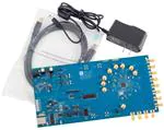


 工商网监
湘ICP备2023018690号
工商网监
湘ICP备2023018690号
