Quad, 16-Bit, 125 MSPS, JESD204B
1.8 V Analog-to-Digital Converter
AD9656
Data Sheet
FUNCTIONAL BLOCK DIAGRAM
VINB+
VINB–
RBIAS
VREF
PIPELINE
ADC
PIPELINE
ADC
SENSE
REF
SELECT
DVDD
16
DRVDD
16
1V
TO
1.4V
SERDOUT0+
SERDOUT0–
JESD204B
INTERFACE
CML TX
OUTPUTS
PIPELINE
ADC
VCM
SERIAL PORT
INTERFACE
16
CONTROL
REGISTERS
CLOCK
MANAGEMENT
AD9656
DVSS
VIND+
VIND–
16
CLK+/
CLK–
PIPELINE
ADC
SERDOUT2+
SERDOUT2–
SYNCINB+
SYNCINB–
AGND
VINC+
VINC–
SERDOUT1+
SERDOUT1–
SERDOUT3+
SERDOUT3–
HIGH
SPEED
SERIALIZERS
SYSREF+/
SYSREF–
Medical ultrasound and MRI
High speed imaging
Quadrature radio receivers
Diversity radio receivers
Portable test equipment
Figure 1.
The AD9656 is available in an RoHS compliant, nonmagnetic,
56-lead LFCSP. It is specified over the −40°C to +85°C
industrial temperature range.
GENERAL DESCRIPTION
The AD9656 is a quad, 16-bit, 125 MSPS analog-to-digital
converter (ADC) with an on-chip sample and hold circuit
designed for low cost, low power, small size, and ease of use.
The device operates at a conversion rate of up to 125 MSPS and
is optimized for outstanding dynamic performance and low
power in applications where a small package size is critical.
The ADC requires a single 1.8 V power supply and LVPECL-/
CMOS-/LVDS-compatible sample rate clock for full performance
operation. An external reference or driver components are not
required for many applications.
Individual channel power-down is supported and typically
consumes less than 14 mW when all channels are disabled. The
ADC contains several features designed to maximize flexibility
and minimize system cost, such as a programmable output clock,
data alignment, and digital test pattern generation. The available
digital test patterns include built-in deterministic and pseudorandom patterns, along with custom user-defined test patterns
entered via the serial port interface (SPI).
Rev. A
VINA+
VINA–
PDWN
CSB
SDIO
SCLK
SVDD
APPLICATIONS
AVDD
SYNC
SNR = 79.9 dBFS at 16 MHz (VREF = 1.4 V)
SNR = 78.1 dBFS at 64 MHz (VREF = 1.4 V)
SFDR = 86 dBc to Nyquist (VREF = 1.4 V)
JESD204B Subclass 1 coded serial digital outputs
Flexible analog input range: 2.0 V p-p to 2.8 V p-p
1.8 V supply operation
Low power: 197 mW per channel at 125 MSPS (two lanes)
DNL = ±0.6 LSB (VREF = 1.4 V)
INL = ±4.5 LSB (VREF = 1.4 V)
650 MHz analog input bandwidth, full power
Serial port control
Full chip and individual channel power-down modes
Built-in and custom digital test pattern generation
Multichip sync and clock divider
Standby mode
11868-001
FEATURES
PRODUCT HIGHLIGHTS
1. It has a small footprint. Four ADCs are contained in a small,
8 mm × 8 mm package.
2. An on-chip phase-locked loop (PLL) allows users to provide
a single ADC sampling clock; the PLL multiplies the ADC
sampling clock to produce the corresponding JESD204B
data rate clock.
3. The configurable JESD204B output block supports up to
8.0 Gbps per lane.
4. JESD204B output block supports one, two, and four lane
configurations.
5. Low power of 198 mW per channel at 125 MSPS, two lanes.
6. The SPI control offers a wide range of flexible features to
meet specific system requirements.
Document Feedback
Information furnished by Analog Devices is believed to be accurate and reliable. However, no
responsibility is assumed by Analog Devices for its use, nor for any infringements of patents or other
rights of third parties that may result from its use. Specifications subject to change without notice. No
license is granted by implication or otherwise under any patent or patent rights of Analog Devices.
Trademarks and registered trademarks are the property of their respective owners.
One Technology Way, P.O. Box 9106, Norwood, MA 02062-9106, U.S.A.
Tel: 781.329.4700 ©2013–2017 Analog Devices, Inc. All rights reserved.
Technical Support
www.analog.com
�AD9656
Data Sheet
TABLE OF CONTENTS
Features .............................................................................................. 1
Analog Input Considerations ................................................... 21
Applications ....................................................................................... 1
Voltage Reference ....................................................................... 23
General Description ......................................................................... 1
Clock Input Considerations ...................................................... 24
Functional Block Diagram .............................................................. 1
Power Dissipation and Power-Down Mode ........................... 26
Product Highlights ........................................................................... 1
Digital Outputs ........................................................................... 26
Revision History ............................................................................... 2
Serial Port Interface (SPI) .............................................................. 35
Specifications..................................................................................... 3
Configuration Using the SPI ..................................................... 35
DC Specifications, VREF = 1.4 V .................................................. 3
Hardware Interface..................................................................... 35
DC Specifications, VREF = 1.0 V .................................................. 4
SPI Accessible Features .............................................................. 35
AC Specifications, VREF = 1.4 V .................................................. 5
Memory Map .................................................................................. 37
AC Specifications, VREF = 1.0 V .................................................. 6
Reading the Memory Map Register Table............................... 37
Digital Specifications ................................................................... 7
Memory Map Register Table ..................................................... 38
Switching Specifications .............................................................. 8
Memory Map Register Descriptions ........................................ 42
Timing Specifications .................................................................. 9
Applications Information .............................................................. 44
Absolute Maximum Ratings.......................................................... 11
Design Guidelines ...................................................................... 44
Thermal Resistance .................................................................... 11
Power and Ground Recommendations ................................... 44
ESD Caution ................................................................................ 11
Clock Stability Considerations ................................................. 44
Pin Configuration and Function Descriptions ........................... 12
Exposed Pad Thermal Heat Slug Recommendations ............ 44
Typical Performance Characteristics ........................................... 14
Reference Decoupling ................................................................ 44
VREF = 1.4 V ................................................................................. 14
SPI Port ........................................................................................ 44
VREF = 1.0 V ................................................................................. 17
Outline Dimensions ....................................................................... 45
Equivalent Circuits ......................................................................... 20
Ordering Guide .......................................................................... 45
Theory of Operation ...................................................................... 21
REVISION HISTORY
3/2017—Rev. 0 to Rev. A
Changed DSYNC to SYNCINB, to SYSREF, DSYNC± to
SYNCINB±, and DSYSREF± to SYSREF± .................... Throughout
Changes to Applications Section, General Description Section, and
Product Highlights Section................................................................ 1
Changes to Table 1 ............................................................................ 3
Changes to Table 2 ............................................................................ 4
Changes to AC Specifications, VREF = 1.4 V Section and Table 3 .... 5
Change to AC Specifications, VREF = 1.0 V Section ..................... 6
Changes to Worst Other Spur or Harmonic (Excluding Second
or Third) Parameter, Table 4, Digital Specifications Section,
and Table 5 ......................................................................................... 7
Changes to Table 6 ............................................................................ 8
Changes to Table 6 Endnotes .......................................................... 9
Changes to Figure 2 Caption ........................................................... 10
Change to Table 8 ........................................................................... 11
Changes to Table 10 ........................................................................ 12
Changes to Figure 39, Figure 41, Figure 41 Caption,
and Figure 44 ................................................................................... 20
Added Figure 42, Renumbered Sequentially .............................. 20
Changes to Input Clock Divider Section..................................... 25
Changes to Power Dissipation and Power-Down Mode Section ... 26
Change to JESD204B Transmit Top Level Description Section ..... 26
Added JESD204B Configurations Section Title, Initial JESD204B
Link Startup Section, and Figure 65.................................................. 27
Added Resynchronization Section and Figure 66 ......................... 28
Changes to CGS Phase Section and ILAS Phase Section ............ 29
Added Figure 67 ....................................................................................... 29
Change to Set Additional Digital Output Configuration
Options Section ........................................................................................ 31
Changes to Figure 68 and Figure 68 ..................................................... 32
Changes to Digital Outputs and Timing Section and Figure 71..... 33
Changes to Hardware Interface Section .............................................. 35
Changes to Table 19 ................................................................................. 39
Change to Transfer (Register 0xFF) Section ................................... 42
Changes to Resolution/Sample Rate Override (Register 0x100) .... 43
Changes to Power and Ground Recommendations Section and
Clock Stability Considerations Section ............................................ 44
12/2013—Revision 0: Initial Version
Rev. A | Page 2 of 46
�Data Sheet
AD9656
SPECIFICATIONS
DC SPECIFICATIONS, VREF = 1.4 V
AVDD = 1.8 V, DRVDD = 1.8 V, 2.8 V p-p full-scale differential input, 1.4 V reference, AIN = −1.0 dBFS, unless otherwise noted.
Table 1.
Parameter 1
RESOLUTION
ACCURACY
No Missing Codes
Offset Error
Offset Matching
Gain Error
Gain Matching
Differential Nonlinearity (DNL)
Integral Nonlinearity (INL)
TEMPERATURE DRIFT
Gain Error
Offset Error
INTERNAL VOLTAGE REFERENCE
Output Voltage
Load Regulation at 1.0 mA
Input Resistance
INPUT REFERRED NOISE
VREF = 1.4 V
ANALOG INPUTS
Differential Input Voltage
Common-Mode Voltage
Common-Mode Range
Differential Input Resistance
Differential Input Capacitance
POWER SUPPLY
AVDD
DVDD, DRVDD
SVDD
IAVDD (125 MSPS, Two Lanes) 2
IDVDD (125 MSPS, Two Lanes)2
IDRVDD (125 MSPS, Two Lanes)2
TOTAL POWER CONSUMPTION
DC Input (125 MSPS, Four Channels onto Two Lanes)
Sine Wave Input (125 MSPS, Four Channels onto Two Lanes)2
Power-Down Mode
Standby Mode 3
Temperature
Min
Full
Full
Full
Full
Full
Full
Full
−0.1
0
−2.0
0
−0.95
−10.0
Full
Full
25°C
25°C
25°C
Typ
16
Guaranteed
+0.14
0.1
+2.1
1.4
±0.6
±4.5
Max
Unit
Bits
+0.5
0.4
+6.0
5.0
+2.54
+10.0
% FSR
% FSR
% FSR
% FSR
LSB
LSB
12.3
−2
1.37
1.4
4
7.5
ppm/°C
ppm/°C
1.41
V
mV
kΩ
25°C
2.1
LSB rms
Full
Full
25°C
25°C
25°C
2.8
0.9
1.1
V p-p
V
V
kΩ
pF
1.9
1.9
3.6
306
72
88
V
V
V
mA
mA
mA
Full
Full
Full
Full
Full
Full
25°C
Full
25°C
25°C
0.7
2.6
7
1.7
1.7
1.7
1.8
1.8
288
67
83
706
788
14
547
839
See the AN-835 Application Note, Understanding High Speed ADC Testing and Evaluation, for definitions and for details on how these tests were completed.
Measured with a low input frequency, full-scale sine wave on all four channels.
3
Standby can be controlled via the SPI.
1
2
Rev. A | Page 3 of 46
mW
mW
mW
mW
�AD9656
Data Sheet
DC SPECIFICATIONS, VREF = 1.0 V
AVDD = 1.8 V, DRVDD = 1.8 V, 2.0 V p-p full-scale differential input, 1.0 V reference, AIN = −1.0 dBFS, unless otherwise noted.
Table 2.
Parameter 1
RESOLUTION
ACCURACY
No Missing Codes
Offset Error
Offset Matching
Gain Error
Gain Matching
Differential Nonlinearity (DNL)
Integral Nonlinearity (INL)
TEMPERATURE DRIFT
Gain Error
Offset Error
INTERNAL VOLTAGE REFERENCE
Output Voltage
Load Regulation at 1.0 mA
Input Resistance
INPUT REFERRED NOISE
VREF = 1.0 V
ANALOG INPUTS
Differential Input Voltage
Common-Mode Voltage
Common-Mode Range
Differential Input Resistance
Differential Input Capacitance
POWER SUPPLY
AVDD
DVDD, DRVDD
SVDD
IAVDD (125 MSPS, Two Lanes) 2
IDVDD (125 MSPS, Two Lanes)2
IDRVDD (125 MSPS, Two Lanes)2
TOTAL POWER CONSUMPTION
DC Input (125 MSPS, Four Channels onto Two Lanes)
Sine Wave Input (125 MSPS, Four Channels onto Two Lanes)
Power-Down Mode
Standby Mode 3
Temperature
Min
Typ
16
Max
Unit
Bits
25°C
25°C
25°C
25°C
25°C
25°C
25°C
Guaranteed
0.2
0.13
1.8
1.4
±0.6
±6.0
% FSR
% FSR
% FSR
% FSR
LSB
LSB
Full
Full
6.3
−3
ppm/°C
ppm/°C
25°C
25°C
25°C
1.0
2
7.5
V
mV
kΩ
25°C
2.7
LSB rms
Full
Full
25°C
25°C
25°C
2.0
0.9
V p-p
V
V
kΩ
pF
Full
Full
Full
25°C
25°C
25°C
25°C
25°C
25°C
25°C
0.5
1.3
2.6
7
1.7
1.7
1.7
1.8
1.8
1.9
1.9
3.6
276
69
83
V
V
V
mA
mA
mA
688
771
14
520
mW
mW
mW
mW
See the AN-835 Application Note, Understanding High Speed ADC Testing and Evaluation, for definitions and for details on how these tests were completed.
Measured with a low input frequency, full-scale sine wave on all four channels.
3
Standby can be controlled via the SPI.
1
2
Rev. A | Page 4 of 46
�Data Sheet
AD9656
AC SPECIFICATIONS, VREF = 1.4 V
AVDD = 1.8 V, DRVDD = 1.8 V, 2.8 V p-p full-scale differential input, 1.4 V reference, AIN = −1.0 dBFS, 125 MSPS, unless otherwise noted.
Table 3.
Parameter 1
SIGNAL-TO-NOISE RATIO (SNR)
fIN = 9.7 MHz
fIN = 16 MHz
fIN = 64 MHz
fIN = 128 MHz
fIN = 201 MHz
fIN = 301 MHz
SIGNAL-TO-NOISE-AND-DISTORTION (SINAD) RATIO
fIN = 9.7 MHz
fIN = 16 MHz
fIN = 64 MHz
fIN = 128 MHz
fIN = 201 MHz
fIN = 301 MHz
EFFECTIVE NUMBER OF BITS (ENOB)
fIN = 9.7 MHz
fIN = 16 MHz
fIN = 64 MHz
fIN = 128 MHz
fIN = 201 MHz
fIN = 301 MHz
SPURIOUS-FREE DYNAMIC RANGE (SFDR)
fIN = 9.7 MHz
fIN = 16 MHz
fIN = 64 MHz
fIN = 128 MHz
fIN = 201 MHz
fIN = 301 MHz
WORST HARMONIC (SECOND OR THIRD)
fIN = 9.7 MHz
fIN = 16 MHz
fIN = 64 MHz
fIN = 128 MHz
fIN = 201 MHz
fIN = 301 MHz
WORST OTHER SPUR OR HARMONIC (EXCLUDING SECOND OR THIRD)
fIN = 9.7 MHz
fIN = 16 MHz
fIN = 64 MHz
fIN = 128 MHz
fIN = 201 MHz
fIN = 301 MHz
Rev. A | Page 5 of 46
Temperature
25°C
25°C
Full
25°C
25°C
25°C
Min
Typ
Max
Unit
80.1
79.9
78.1
75
72.7
69.7
dBFS
dBFS
dBFS
dBFS
dBFS
dBFS
79.6
78.4
77.3
74.4
71
68.6
dBFS
dBFS
dBFS
dBFS
dBFS
dBFS
12.9
12.7
12.5
12.1
11.5
11.1
Bits
Bits
Bits
Bits
Bits
Bits
89
87
86
84
76
75
dBc
dBc
dBc
dBc
dBc
dBc
25°C
25°C
Full
25°C
25°C
25°C
−89
−87
−86
−84
−76
−75
dBc
dBc
dBc
dBc
dBc
dBc
25°C
25°C
Full
25°C
25°C
25°C
−96
−92
−90
−89
−93
−90
25°C
25°C
Full
25°C
25°C
25°C
25°C
25°C
Full
25°C
25°C
25°C
25°C
25°C
Full
25°C
25°C
25°C
75.7
74.8
12.1
78
−78
−87
dBc
dBc
dBc
dBc
dBc
dBc
�AD9656
Data Sheet
Parameter1
TWO-TONE INTERMODULATION DISTORTION (IMD)—INPUT AMPLITUDE = −7.0 dBFS
fIN1 = 70.5 MHz, fIN2 = 72.5 MHz
CROSSTALK2
CROSSTALK (OVERRANGE CONDITION)3
ANALOG INPUT BANDWIDTH, FULL POWER
Temperature
Min
25°C
25°C
25°C
25°C
Typ
Max
−84
−93
−89
650
Unit
dBc
dB
dB
MHz
1
See the AN-835 Application Note, Understanding High Speed ADC Testing and Evaluation, for definitions and for details on how these tests were completed.
Crosstalk is measured at 70 MHz with −1.0 dBFS analog input on one channel and no input on the adjacent channel.
3
Overrange condition is defined as the input being 3 dB above full scale.
2
AC SPECIFICATIONS, VREF = 1.0 V
AVDD = 1.8 V, DRVDD = 1.8 V, 2.0 V p-p full-scale differential input, 1.0 V reference, AIN = −1.0 dBFS, 125 MSPS, unless otherwise noted.
Table 4.
Parameter1
SIGNAL-TO-NOISE RATIO (SNR)
fIN = 9.7 MHz
fIN = 16 MHz
fIN = 64 MHz
fIN = 128 MHz
fIN = 201 MHz
fIN = 301 MHz
SIGNAL-TO-NOISE-AND-DISTORTION (SINAD) RATIO
fIN = 9.7 MHz
fIN = 16 MHz
fIN = 64 MHz
fIN = 128 MHz
fIN = 201 MHz
fIN = 301 MHz
EFFECTIVE NUMBER OF BITS (ENOB)
fIN = 9.7 MHz
fIN = 16 MHz
fIN = 64 MHz
fIN = 128 MHz
fIN = 201 MHz
fIN = 301 MHz
SPURIOUS-FREE DYNAMIC RANGE (SFDR)
fIN = 9.7 MHz
fIN = 16 MHz
fIN = 64 MHz
fIN = 128 MHz
fIN = 201 MHz
fIN = 301 MHz
WORST HARMONIC (SECOND OR THIRD)
fIN = 9.7 MHz
fIN = 16 MHz
fIN = 64 MHz
fIN = 128 MHz
fIN = 201 MHz
fIN = 301 MHz
Temperature
Rev. A | Page 6 of 46
Min
Typ
Max
Unit
25°C
25°C
25°C
25°C
25°C
25°C
78
77.9
76.8
74.3
72.1
69.3
dBFS
dBFS
dBFS
dBFS
dBFS
dBFS
25°C
25°C
25°C
25°C
25°C
25°C
78
77.7
76.1
74
71.1
68.6
dBFS
dBFS
dBFS
dBFS
dBFS
dBFS
25°C
25°C
25°C
25°C
25°C
25°C
12.7
12.6
12.3
12.0
11.5
11.1
Bits
Bits
Bits
Bits
Bits
Bits
25°C
25°C
25°C
25°C
25°C
25°C
99
92
89
87
78
78
dBc
dBc
dBc
dBc
dBc
dBc
25°C
25°C
25°C
25°C
25°C
25°C
−99
−92
−89
−87
−78
−78
dBc
dBc
dBc
dBc
dBc
dBc
�Data Sheet
AD9656
Parameter 1
WORST OTHER SPUR OR HARMONIC (EXCLUDING SECOND OR THIRD)
fIN = 9.7 MHz
fIN = 16 MHz
fIN = 64 MHz
fIN = 128 MHz
fIN = 201 MHz
fIN = 301 MHz
TWO-TONE INTERMODULATION DISTORTION (IMD)—INPUT AMPLITUDE = −7.0 dBFS
fIN1 = 70.5 MHz, fIN2 = 72.5 MHz
CROSSTALK 2
CROSSTALK (OVERRANGE CONDITION) 3
ANALOG INPUT BANDWIDTH, FULL POWER
Temperature
Min
Typ
Max
Unit
25°C
25°C
25°C
25°C
25°C
25°C
−95
−95
−94
−89
−91
−89
dBc
dBc
dBc
dBc
dBc
dBc
25°C
25°C
25°C
25°C
−89
−94
−89
650
dBc
dB
dB
MHz
See the AN-835 Application Note, Understanding High Speed ADC Testing and Evaluation, for definitions and for details on how these tests were completed.
Crosstalk is measured at 70 MHz with −1.0 dBFS analog input on one channel and no input on the adjacent channel.
3
Overrange condition is defined as the input being 3 dB above full-scale.
1
2
DIGITAL SPECIFICATIONS
AVDD = 1.8 V, DRVDD = 1.8 V, SVDD = 1.8 V, 2.8 V p-p differential input, 1.4 V reference, AIN = −1.0 dBFS, unless otherwise noted.
Table 5.
Parameter 1
CLOCK INPUTS (CLK±)
Logic Compliance
Differential Input Voltage Range 2
Input Voltage Range
Input Common-Mode Voltage
Input Resistance (Differential)
Input Capacitance
SYNCINB INPUT (SYNCINB±)
Logic Compliance
Internal Common-Mode Bias
Differential Input Voltage Range
Input Voltage Range
Input Common-Mode Voltage Range
High Level Input Current
Low Level Input Current
Input Capacitance
Input Resistance
SYSREF INPUT (SYSREF±)
Logic Compliance
Internal Common-Mode Bias
Differential Input Voltage Range
Input Voltage Range
Input Common-Mode Voltage Range
High Level Input Current
Low Level Input Current
Input Capacitance
Input Resistance
LOGIC INPUT (SYNC)
Logic 1 Voltage Range
Logic 0 Voltage Range
Input Resistance
Input Capacitance
Temperature
Min
Full
Full
Full
25°C
25°C
0.2
AGND − 0.2
Typ
Max
Unit
3.6
AVDD + 0.2
V p-p
V
V
kΩ
pF
CMOS/LVDS/LVPECL
0.9
15
4
LVDS
Full
Full
Full
Full
Full
Full
Full
Full
0.9
0.3
DGND
0.9
−5
−5
12
3.6
DVDD
1.4
+5
+5
1
16
20
V
V p-p
V
V
µA
µA
pF
kΩ
LVDS
Full
Full
Full
Full
Full
Full
Full
Full
Full
Full
25°C
25°C
0.9
0.3
AGND
0.9
−5
−5
8
3.6
AVDD
1.4
+5
+5
4
10
1.2
0
Rev. A | Page 7 of 46
12
AVDD + 0.2
0.8
30
2
V
V p-p
V
V
µA
µA
pF
kΩ
V
V
kΩ
pF
�AD9656
Parameter 1
LOGIC INPUTS (CSB, PDWN, SCLK)
Logic 1 Voltage Range
Logic 0 Voltage Range
Input Resistance
Input Capacitance
LOGIC INPUT (SDIO)
Logic 1 Voltage Range
Logic 0 Voltage Range
Input Resistance
Input Capacitance
LOGIC OUTPUT (SDIO) 3
Logic 1 Voltage (IOH = 800 µA)
Logic 0 Voltage (IOL = 50 µA)
DIGITAL OUTPUTS (SERDOUTx±)
Logic Compliance
Differential Output Voltage (VOD)
Output Offset Voltage (VOS)
1
2
3
Data Sheet
Temperature
Min
Full
Full
25°C
25°C
1.2
0
Full
Full
25°C
25°C
1.2
0
Max
Unit
SVDD + 0.2
0.8
V
V
kΩ
pF
SVDD + 0.2
0.8
V
V
kΩ
pF
26
2
26
5
Full
Full
Full
Full
Full
Typ
1.79
400
0.75
CML
600
DRVDD/2
0.05
V
V
750
1.05
mV
V
See the AN-835 Application Note, Understanding High Speed ADC Testing and Evaluation, for definitions and for details on how these tests were completed.
Specified for LVDS and LVPECL only.
Specified for the SDIO pins on 13 individual AD9656 devices sharing the same connection.
SWITCHING SPECIFICATIONS
AVDD = 1.8 V, DRVDD = 1.8 V, 2.8 V p-p differential input, 1.4 V reference, AIN = −1.0 dBFS, unless otherwise noted.
Table 6.
Parameter 1, 2
CLOCK 3
Input Clock Rate
Conversion Rate 4
Clock Pulse Width High (tEH)
Clock Pulse Width Low (tEL)
SYNC Setup Time to Clock
SYNC Hold Time to Clock
SYSREF Setup Time to Clock (tREFS) 5
SYSREF Hold Time to Clock (tREFH)5
DATA OUTPUT PARAMETERS
Data Output Period or Unit Interval (UI)
Data Output Duty Cycle
Data Valid Time
PLL Lock Time (tLOCK) 6
Wake-Up Time
Standby
ADC (Power-Down) 7
Output (Power-Down) 8
SYNCINB Falling Edge to First K.28 Characters
CGS Phase K.28 Characters Duration
Subclass 1: SYSREF Rising Edge to First Valid K.28 Characters 9
Pipeline Delay
JESD204B M4, L1 Mode (Latency)
JESD204B M4, L2 Mode (Latency)
JESD204B M4, L4 Mode (Latency)
Data Rate per Lane
Temperature
Min
Full
Full
Full
Full
Full
Full
Full
Full
40
40
Full
Full
Full
Full
Rev. A | Page 8 of 46
Max
Unit
1000
125
MHz
MSPS
ns
ns
ns
ns
ps
ps
4.00
4.00
370
−92
Full
25°C
25°C
25°C
25°C
25°C
25°C
Full
Full
Full
Typ
1.4
−0.4
600
0
L/(20 × M × fS)
50
0.81
86
250
375
86
4
1
5
Seconds
%
UI
µs
6
ns
µs
µs
Multiframes
Multiframe
Multiframe
8.0
Cycles 10
Cycles10
Cycles10
Gbps
23
29
44
�Data Sheet
AD9656
Parameter 1, 2
Deterministic Jitter (DJ)
At 6.4 Gbps
Random Jitter (RJ)
At 6.4 Gbps
Output Rise Time/Fall Time
Differential Termination Resistance
APERTURE
Aperture Delay (tA)
Aperture Uncertainty (Jitter, tJ)
Out of Range Recovery Time
Temperature
Min
Typ
Max
Unit
25°C
8
ps
25°C
25°C
25°C
1.25
50
100
ps rms
ps
Ω
25°C
25°C
25°C
1
135
1
ns
fs rms
Clock cycles
See the AN-835 Application Note, Understanding High Speed ADC Testing and Evaluation, for definitions and for details on how these tests were completed.
Measured on standard FR-4 material.
3
The clock divider can be adjusted via the SPI. The conversion rate is the clock rate after the divider.
4
Maximum conversion rate is with the AD9656 not limited by the maximum allowable output data rate. See the Digital Outputs and Timing section for information on
conditions when the conversion rate is limited by the maximum allowable output data rate.
5
Refer to Figure 3 for timing diagram.
6
Typical PLL lock time at 125 MSPS (24 μs + 7680 sample clock periods)
7
Time required for the ADC to return to normal operation from power-down mode.
8
Time required for the JESD204B output to return to normal operation from power-down mode at 125 MSPS (PLL lock time + 13 sample clock periods)
9
Delay required for SYNCINB rising edge/Rx CGS start. See Figure 66.
10
ADC conversion rate cycles.
1
2
TIMING SPECIFICATIONS
Table 7.
Parameter
SPI TIMING REQUIREMENTS
tDS
tDH
tCLK
tS
tH
tHIGH
tLOW
tEN_SDIO
tDIS_SDIO
Description
See Figure 74
Setup time between the data and the rising edge of SCLK
Hold time between the data and the rising edge of SCLK
Period of the SCLK
Setup time between CSB and SCLK
Hold time between CSB and SCLK
SCLK pulse width high
SCLK pulse width low
Time required for the SDIO pin to switch from an input to an output relative to the
SCLK falling edge (not shown in Figure 74)
Time required for the SDIO pin to switch from an output to an input relative to the
SCLK rising edge (not shown in Figure 74)
Rev. A | Page 9 of 46
Limit
Unit
2
2
40
2
2
10
10
10
ns min
ns min
ns min
ns min
ns min
ns min
ns min
ns min
10
ns min
�AD9656
Data Sheet
Timing Diagrams
Refer to the Memory Map Register Table section for SPI register settings.
SAMPLE N
N – 23
VINA+/
VINA–
N+1
N – 22
N – 21
N – 20
N – 19
N–1
SAMPLE N
N – 23
N+1
N – 22
VINB+/
VINB–
N – 21
N – 20
N – 19
N–1
SAMPLE N
N – 23
VINC+/
VINC–
N+1
N – 22
N – 21
N – 20
N – 19
N–1
SAMPLE N
N – 23
VIND+/
VIND–
N+1
N – 22
N – 21
N – 20
N – 19
N–1
CLK–
CLK+
CLK–
CLK+
SERDOUTx–
SERDOUTx+
VINB, SAMPLE N – 23,
MSB FIRST, 8B/10B
ENCODED DATA
VINC, SAMPLE N – 23,
MSB FIRST, 8B/10B
ENCODED DATA
VIND, SAMPLE N – 23,
MSB FIRST, 8B/10B
ENCODED DATA
11868-002
VINA, SAMPLE N – 23,
MSB FIRST, 8B/10B
ENCODED DATA
Figure 2. Data Output Timing, M = 4, L = 1
CLK+
CLK–
tREFS
tREFH
11868-003
SYSREF–
SYSREF+
Figure 3. SYSREF± Setup and Hold Timing (Clock Divider = 1)
Rev. A | Page 10 of 46
�Data Sheet
AD9656
ABSOLUTE MAXIMUM RATINGS
THERMAL RESISTANCE
Table 8.
Parameter
Electrical
AVDD to AGND
DRVDD to AGND
DVDD to DVSS
SVDD to AGND
Digital Outputs to AGND
CLK+, CLK− to AGND
VINx+, VINx− to AGND
SYSREF± to AGND
SYNCINB± to AGND
SCLK, SDIO, CSB, PDWN to AGND
SYNC to AGND
RBIAS to AGND
VCM, VREF, SENSE to AGND
Environmental
Operating Temperature Range (Ambient)
Maximum Junction Temperature
Lead Temperature (Soldering, 10 sec)
Storage Temperature Range (Ambient)
θJA is for a 4-layer printed circuit board (PCB) with solid ground
plane (simulated). The exposed pad is soldered to the PCB ground.
Rating
−0.3 V to +2.0 V
−0.3 V to +2.0 V
−0.3 V to +2.0 V
−0.3 V to +3.9 V
−0.3 V to +2.0 V
−0.3 V to +2.0 V
−0.3 V to +2.0 V
−0.3 V to +2.0 V
−0.3 V to +2.0 V
−0.3 V to +3.9 V
−0.3 V to +2.0 V
−0.3 V to +2.0 V
−0.3 V to +2.0 V
Table 9. Thermal Resistance
Package
Type
56-Lead
LFCSP,
8 mm ×
8 mm
1
Air Flow
Velocity
(m/sec)
0
1
2.5
N/A means not applicable.
ESD CAUTION
−40°C to +85°C
150°C
300°C
−65°C to +150°C
Stresses at or above those listed under Absolute Maximum
Ratings may cause permanent damage to the product. This is a
stress rating only; functional operation of the product at these
or any other conditions above those indicated in the operational
section of this specification is not implied. Operation beyond
the maximum operating conditions for extended periods may
affect product reliability.
Rev. A | Page 11 of 46
θJA
(°C/W)
22.4
19.0
17.6
θJB
(°C/W)1
7.7
N/A
N/A
θJC Top
(°C/W)1
7.42
N/A
N/A
θJC Bottom
(°C/W)1
2.29
N/A
N/A
�AD9656
Data Sheet
1
2
VIND–
AVDD
AVDD
3
4
5
CLK–
CLK+
AVDD
SYSREF+
6
7
8
9
44 VINB+
43 AVDD
47 RBIAS
46 AVDD
45 VINB–
SYNC
VCM
VREF
SENSE
51
50
49
48
52 AVDD
42 AVDD
41 VINA+
40 VINA–
39 AVDD
38 PDWN
37 CSB
AD9656
TOP VIEW
SYSREF– 10
AVDD 11
DVDD 12
DVSS 13
SDIO
SCLK
DNC
SVDD
32
31
30
29
DVDD
DVSS
NIC
NIC
DRVDD 28
SERDOUT0+ 26
SERDOUT0– 27
SERDOUT1+ 25
DRVDD 23
SERDOUT1– 24
SERDOUT3– 19
SERDOUT3+ 20
SERDOUT2+ 21
SERDOUT2– 22
NIC 15
SYNCINB+ 16
SYNCINB– 17
DRVDD 18
NIC 14
36
35
34
33
NOTES
1. NIC = NOT INTERNALLY CONNECTED. CAN BE CONNECTED TO GROUND IF DESIRED.
2. DNC = DO NOT CONNECT. DO NOT CONNECT TO THIS PIN.
3. THE EXPOSED THERMAL PAD ON THE BOTTOM OF THE PACKAGE PROVIDES
THE ANALOG GROUND FOR THE PART. THIS EXPOSED PAD MUST BE
CONNECTED TO GROUND FOR PROPER OPERATION.
11868-004
AVDD
VIND+
55 VINC+
54 VINC–
53 AVDD
56 AVDD
PIN CONFIGURATION AND FUNCTION DESCRIPTIONS
Figure 4. Pin Configuration, Top View
Table 10. Pin Function Descriptions
Pin No.
0
1, 4, 5, 8, 11, 39, 42,
43, 46, 52, 53, 56
2
3
6, 7
9
10
12, 32
13, 31
14, 15, 29, 30
16
17
18, 23, 28
19
20
21
22
24
25
26
27
33
Mnemonic
AGND,
Exposed Pad
AVDD
Description
Analog Ground, Exposed Pad. The exposed thermal pad on the bottom of the package provides the
analog ground for the device. This exposed pad must be connected to ground for proper operation.
1.8 V Analog Supply Pins.
VIND+
VIND−
CLK−, CLK+
SYSREF+
SYSREF−
DVDD
DVSS
NIC
SYNCINB+
SYNCINB−
DRVDD
SERDOUT3−
SERDOUT3+
SERDOUT2+
SERDOUT2−
SERDOUT1−
SERDOUT1+
SERDOUT0+
SERDOUT0−
SVDD
ADC D Analog Input True.
ADC D Analog Input Complement.
Differential Encode Clock. PECL, LVDS, or 1.8 V CMOS inputs.
Active High JESD204B LVDS SYSREF Input True.
Active High JESD204B LVDS SYSREF Input Complement.
Digital Supply.
Digital Ground.
Not Internally Connected. Can be connected to ground if desired.
Active Low JESD204B LVDS SYNC Input True.
Active Low JESD204B LVDS SYNC Input Complement.
Digital Output Driver Supply.
Lane 3 Digital Output Complement.
Lane 3 Digital Output True.
Lane 2 Digital Output True.
Lane 2 Digital Output Complement.
Lane 1 Digital Output Complement.
Lane 1 Digital Output True.
Lane 0 Digital Output True.
Lane 0 Digital Output Complement.
SPI Supply Pin.
Rev. A | Page 12 of 46
�Data Sheet
AD9656
Pin No.
34
35
36
37
38
Mnemonic
DNC
SCLK
SDIO
CSB
PDWN
40
41
44
45
47
48
49
50
51
54
55
VINA−
VINA+
VINB+
VINB−
RBIAS
SENSE
VREF
VCM
SYNC
VINC−
VINC+
Description
Do Not Connect. Do not connect to this pin.
SPI Clock Input.
SPI Data Input and Output, Bidirectional.
SPI Chip Select Bar. Active low enable; 30 kΩ internal pull-up resistor.
Digital Input. This pin has a 30 kΩ internal pull-down resistor. PDWN high = power-down device and
PDWN low = run device (normal operation).
ADC A Analog Input Complement.
ADC A Analog Input True.
ADC B Analog Input True.
ADC B Analog Input Complement.
Sets Analog Current Bias. This pin connects a 10 kΩ (1% tolerance) resistor to ground.
Reference Mode Selection.
Voltage Reference Input and Output.
Analog Input Common-Mode Voltage.
Digital Input. Synchronous input to clock divider.
ADC C Analog Input Complement.
ADC C Analog Input True.
Rev. A | Page 13 of 46
�AD9656
Data Sheet
TYPICAL PERFORMANCE CHARACTERISTICS
VREF = 1.4 V
0
–20
–40
–60
–80
–100
–40
–60
–80
–100
–120
40
60
FREQUENCY (MHz)
–140
0
AMPLITUDE (dBFS)
–60
–80
–40
–60
–80
–100
–100
–120
–120
0
20
40
60
FREQUENCY (MHz)
AIN = –1dBFS
fIN = 201MHz
SNR = 72.6dBFS
SINAD = 70.2dBFS
SFDR = 76dBc
–20
–140
11868-037
AMPLITUDE (dBFS)
0
–40
–140
0
0
AIN = –1dBFS
fIN = 64MHz
SNR = 78.5dBFS
SINAD = 76.4dBFS
SFDR = 83dBc
AMPLITUDE (dBFS)
AMPLITUDE (dBFS)
–60
–80
–40
–60
–80
–100
–120
–120
40
FREQUENCY (MHz)
60
11868-036
–100
20
60
AIN = –1dBFS
fIN = 301MHz
SNR = 69.8dBFS
SINAD = 67.5dBFS
SFDR = 74dBc
–20
–40
0
40
Figure 9. Single-Tone 32k FFT with fIN = 201 MHz,
fSAMPLE = 125 MSPS, VREF = 1.4 V
0
–140
20
FREQUENCY (MHz)
Figure 6. Single-Tone 32k FFT with fIN = 16.3 MHz,
fSAMPLE = 125 MSPS, VREF = 1.4 V
–20
60
Figure 8. Single-Tone 32k FFT with fIN = 128.1 MHz,
fSAMPLE = 125 MSPS, VREF = 1.4 V
AIN = –1dBFS
fIN = 16.3MHz
SNR = 79.9dBFS
SINAD = 78.3dBFS
SFDR = 89dBc
–20
40
FREQUENCY (MHz)
Figure 5. Single-Tone 32k FFT with fIN = 9.7 MHz,
fSAMPLE = 125 MSPS, VREF = 1.4 V
0
20
11868-033
20
Figure 7. Single-Tone 32k FFT with fIN = 64 MHz,
fSAMPLE = 125 MSPS, VREF = 1.4 V
–140
0
20
40
FREQUENCY (MHz)
Figure 10. Single-Tone 32k FFT with fIN = 301 MHz,
fSAMPLE = 125 MSPS, VREF = 1.4 V
Rev. A | Page 14 of 46
60
11868-032
0
11868-034
–120
11868-038
–140
AIN = –1dBFS
fIN = 128.1MHz
SNR = 75.3dBFS
SINAD = 73.3dBFS
SFDR = 81dBc
–20
AMPLITUDE (dBFS)
AMPLITUDE (dBFS)
0
AIN = –1dBFS
fIN = 9.7MHz
SNR = 80.1dBFS
SINAD = 78.7dBFS
SFDR = 92dBc
�Data Sheet
AD9656
100
120
90
SFDR (dBFS)
100
SNR/SFDR (dBFS/dBc)
SNR/SFDR (dBFS/dBc)
SFDR (dBc)
80
SNR (dBFS)
80
SFDR (dBc)
60
40
SNR (dB)
20
70
60
SNR (dBFS)
50
40
30
20
0
–80
–60
–40
–20
0
11868-030
–20
–100
0
INPUT AMPLITUDE (dBFS)
SNR/SFDR (dBFS/dBc)
F1 + 2F2
2F1 + F2
2F2 – F1
F1 + F2
350
400
450
500
SFDR (dBc)
90
SNR (dBFS)
80
70
–120
20
40
60
60
–40
11868-035
0
FREQUENCY (MHz)
–20
0
20
40
60
80
TEMPERATURE (°C)
Figure 12. Two-Tone 32k FFT with fIN1 = 70.5 MHz and fIN2 = 72.5 MHz,
fSAMPLE = 125 MSPS, VREF = 1.4 V
Figure 15. SNR/SFDR vs. Temperature, fIN = 9.7 MHz,
fSAMPLE = 125 MSPS, VREF = 1.4 V
0
6
–20
4
–SFDR (dBc)
–40
2
–60
INL (LSB)
SFDR/IMD3 (dBc/dBFS)
300
11868-023
AMPLITUDE (dBFS)
2F1 – F2
–80
–140
250
100
–60
F2 – F1
200
150
110
AIN = –7dBFS
fIN1 = 70.5MHz
fIN2 = 72.5MHz
IMD2 = –98dBc
IMD3 = –84dBc
SFDR = 84dBc
–100
100
Figure 14. SNR/SFDR vs. Input Frequency (fIN), fSAMPLE = 125 MSPS,
VREF = 1.4 V
0
–40
50
INPUT FREQUENCY (MHz)
Figure 11. SNR/SFDR vs. Input Amplitude (AIN), fIN = 9.7 MHz,
fSAMPLE = 125 MSPS, VREF = 1.4 V
–20
0
11868-025
10
IMD3 (dBc)
0
–80
–2
–SFDR (dBFS)
–100
–4
–80
–70
–60
–50
–40
–30
–20
–10
INPUT AMPLITUDE (dBFS)
Figure 13. Two-Tone SFDR/IMD3 vs. Input Amplitude (AIN) with
fIN1 = 70.5 MHz and fIN2 = 72.5 MHz, fSAMPLE = 125 MSPS, VREF = 1.4 V
–6
0
10000
20000
30000
40000
OUTPUT CODE
50000
60000
11868-015
IMD3 (dBFS)
11868-027
–120
–90
Figure 16. Integral Nonlinearity (INL), fIN = 9.7 MHz, fSAMPLE = 125 MSPS,
VREF = 1.4 V
Rev. A | Page 15 of 46
�AD9656
Data Sheet
120
0.4
100
SNR/SFDR (dBFS/dBc)
0.6
0
–0.2
SNR (dBFS)
80
60
40
20
–0.4
0
10000
20000
30000
40000
50000
60000
OUTPUT CODE
0
11868-016
–0.6
40
60
80
100
120
SAMPLE RATE (MSPS)
11868-019
DNL (LSB)
0.2
SFDR (dBc)
Figure 19. SNR/SFDR vs. Sample Rate, fIN = 9.7 MHz, VREF = 1.4 V
Figure 17. Differential Nonlinearity (DNL), fIN = 9.7 MHz, fSAMPLE = 125 MSPS,
VREF = 1.4 V
120
450000
2.0 LSB RMS
400000
100
SNR/SFDR (dBFS/dBc)
NUMBER OF HITS
350000
300000
250000
200000
150000
SFDR (dBc)
80
SNR (dBFS)
60
40
100000
OUTPUT CODE
11868-021
N – 10
N–9
N–8
N–7
N–6
N–5
N–4
N–3
N–2
N–1
N
N+1
N+2
N+3
N+4
N+5
N+6
N+7
N+8
N+9
N + 10
0
Figure 18. Input Referred Noise Histogram, fSAMPLE = 125 MSPS, VREF = 1.4 V
Rev. A | Page 16 of 46
0
40
50
60
70
80
90
100
110
120
SAMPLE RATE (MSPS)
Figure 20. SNR/SFDR vs. Sample Rate, fIN = 64 MHz, VREF = 1.4 V
11868-017
20
50000
�Data Sheet
AD9656
VREF = 1.0 V
0
AIN = –1dBFS
fIN = 9.7MHz
SNR = 78.0dBFS
SINAD = 77.0dBFS
SFDR = 99dBc
AMPLITUDE (dBFS)
–60
–80
–40
–60
–80
–100
–100
–120
–120
0
20
40
–140
11868-145
–140
60
FREQUENCY (MHz)
0
AMPLITUDE (dBFS)
–60
–80
–40
–60
–80
–100
–100
–120
–120
0
20
40
60
FREQUENCY (MHz)
AIN = –1dBFS
fIN = 201MHz
SNR = 72.2dBFS
SINAD = 70.2dBFS
SFDR = 78dBc
–20
–140
11868-143
AMPLITUDE (dBFS)
0
–40
–140
0
AMPLITUDE (dBFS)
–60
–80
–40
–60
–80
–100
–100
–120
–120
0
20
40
FREQUENCY (MHz)
60
AIN = –1dBFS
fIN = 301MHz
SNR = 69.3dBFS
SINAD = 67.6dBFS
SFDR = 77dBc
–20
60
–140
11868-149
AMPLITUDE (dBFS)
0
–40
–140
40
Figure 25. Single-Tone 32k FFT with fIN = 201 MHz,
fSAMPLE = 125 MSPS, VREF = 1.0 V
AIN = –1dBFS
fIN = 64MHz
SNR = 76.9dBFS
SINAD = 75.7dBFS
SFDR = 90dBc
–20
20
FREQUENCY (MHz)
Figure 22. Single-Tone 32k FFT with fIN = 16.3 MHz,
fSAMPLE = 125 MSPS, VREF = 1.0 V
0
60
Figure 24. Single-Tone 32k FFT with fIN = 128.1 MHz,
fSAMPLE = 125 MSPS, VREF = 1.0 V
AIN = –1dBFS
fIN = 16.3MHz
SNR = 78.0dBFS
SINAD = 76.8dBFS
SFDR = 94dBc
–20
40
FREQUENCY (MHz)
Figure 21. Single-Tone 32k FFT with fIN = 9.7 MHz,
fSAMPLE = 125 MSPS, VREF = 1.0 V
0
20
11868-040
AMPLITUDE (dBFS)
–40
Figure 23. Single-Tone 32k FFT with fIN = 64 MHz, fSAMPLE = 125 MSPS,
VREF = 1.0 V
0
20
40
FREQUENCY (MHz)
60
11868-039
–20
AIN = –1dBFS
fIN = 128.1MHz
SNR = 74.5dBFS
SINAD = 73.0dBFS
SFDR = 84dBc
–20
11868-041
0
Figure 26. Single-Tone 32k FFT with fIN = 301 MHz, fSAMPLE = 125 MSPS,
VREF = 1.0 V
Rev. A | Page 17 of 46
�AD9656
Data Sheet
120
110
SFDR (dBFS)
100
100
SNR/SFDR (dBFS/dBc)
SNR/SFDR (dBFS/dBc)
90
SNR (dBFS)
80
SFDR (dBc)
60
40
SNR (dB)
20
SFDR (dBc)
80
70
SNR (dBFS)
60
50
40
30
20
0
10
–30
–10
INPUT AMPLITUDE (dBFS)
Figure 27. SNR/SFDR vs. Input Amplitude (AIN), fIN = 9.7 MHz,
fSAMPLE = 125 MSPS, VREF = 1.0 V
0
50
100
150
200
250
300
350
400
450
500
INPUT FREQUENCY (MHz)
Figure 30. SNR/SFDR vs. Input Frequency (fIN), fSAMPLE = 125 MSPS, VREF = 1.0 V
110
0
AIN = –7dBFS
fIN1 = 70.5MHz
fIN2 = 72.5MHz
IMD2= –99dBc
IMD3 = –89dBc
SFDR = 89dBc
–40
100
SNR/SFDR (dBFS/dBc)
–20
AMPLITUDE (dBFS)
0
11868-026
–50
–70
11868-031
–20
–90
–60
2F1 – F2
–80
F1 + 2F2
–100
F2 – F1
2F1 + F2
2F2 – F1
SFDR (dBc)
90
80
SNR (dBFS)
F1 + F2
70
0
20
40
FREQUENCY (MHz)
60
–40
11868-029
–140
0
20
40
60
80
TEMPERATURE (°C)
Figure 28. Two-Tone 32k FFT with fIN1 = 70.5 MHz and fIN2 = 72.5 MHz,
fSAMPLE = 125 MSPS, VREF = 1.0 V
Figure 31. SNR/SFDR vs. Temperature, fIN = 9.7 MHz,
fSAMPLE = 125 MSPS, VREF = 1.0 V
0
6
–20
4
–SFDR (dBc)
–40
2
IMD3 (dBc)
INL (LSB)
SFDR/IMD3 (dBc/dBFS)
–20
11868-024
–120
–60
0
–80
–2
–SFDR (dBFS)
–100
–4
–70
–60
–50
–40
–30
–20
–10
INPUT AMPLITUDE (dBFS)
–6
0
10000
20000
30000
40000
OUTPUT CODE
Figure 29. Two-Tone SFDR/IMD3 vs. Input Amplitude (AIN) with
fIN1 = 70.5 MHz and fIN2 = 72.5 MHz, fSAMPLE = 125 MSPS, VREF = 1.0 V
50000
60000
11868-009
–80
11868-028
–120
–90
IMD3 (dBFS)
Figure 32. Integral Nonlinearity (INL), fIN = 9.7 MHz, fSAMPLE = 125 MSPS,
VREF = 1.0 V
Rev. A | Page 18 of 46
�Data Sheet
AD9656
0.6
120
0.4
100
SNR/SFDR (dBFS/dBc)
SFDR (dBc)
0
–0.2
–0.4
60
40
20
20000
10000
0
40000
30000
50000
60000
OUTPUT CODE
0
40
11868-010
–0.6
350000
50
60
70
80
90
100
110
120
SAMPLE RATE (MSPS)
Figure 33. Differential Nonlinearity (DNL), fIN = 9.7 MHz, fSAMPLE = 125 MSPS,
VREF = 1.0 V
Figure 35. SNR/SFDR vs. Sample Rate, fIN = 9.7 MHz, VREF = 1.0 V
120
2.7
2.0 LSB
LSB RMS
RMS
SNR/SFDR (dBFS/dBc)
300000
250000
NUMBER OF HITS
SNR (dBFS)
80
11868-020
DNL (LSB)
0.2
200000
150000
100000
100
SFDR (dBc)
80
SNR (dBFS)
60
40
20
Figure 34. Input Referred Noise Histogram, fSAMPLE = 125 MSPS, VREF = 1.0 V
Rev. A | Page 19 of 46
50
60
70
80
90
100
110
120
SAMPLE RATE (MSPS)
Figure 36. SNR/SFDR vs. Sample Rate, fIN = 64 MHz, VREF = 1.0 V
11868-018
N + 12
N+8
N + 10
N+6
0
40
11868-022
OUTPUT CODE
N+4
N+2
N
N–2
N–4
N–6
N–8
N – 10
0
N – 12
50000
�AD9656
Data Sheet
EQUIVALENT CIRCUITS
AVDD
DVDD
SVDD
VINx±
375Ω
SCLK,
PDWN
11868-142
11868-043
30kΩ
Figure 37. Equivalent Analog Input Circuit
Figure 42. Equivalent SCLK and PDWN Input Circuit
AVDD
10Ω
CLK+
AVDD
15kΩ
0.9V
AVDD
15kΩ
11868-048
11868-044
CLK–
375Ω
RBIAS
AND VCM
10Ω
Figure 38. Equivalent Clock Input Circuit
SVDD
Figure 43. Equivalent RBIAS and VCM Circuit
DVDD
SVDD
DVDD
400Ω
SDIO
30kΩ
31kΩ
11868-049
11868-045
CSB
350Ω
Figure 39. Equivalent SDIO Input Circuit
Figure 44. Equivalent CSB Input Circuit
DRVDD
DRVDD
3mA 3mA
AVDD
DRVDD
RTERM
350Ω
VREF
VCM
SERDOUTx–
11868-148
6mA
11868-050
SERDOUTx+
7.5Ω
Figure 40. Equivalent SERDOUTx± Circuit
Figure 45. Equivalent VREF Circuit
AVDD
SYNC
350Ω
11868-049
30kΩ
Figure 41. Equivalent SYNC Input Circuit
Rev. A | Page 20 of 46
�Data Sheet
AD9656
THEORY OF OPERATION
or ferrite beads is required when driving the converter front end at
high IF frequencies.
The AD9656 is a multistage, pipelined ADC. Each stage
provides sufficient overlap to correct for flash errors in the
preceding stage. The quantized outputs from each stage are
combined into a final 16-bit result in the digital correction
logic. The serializer transmits this converted data in a 16-bit
output. The pipelined architecture permits the first stage to
operate with a new input sample while the remaining stages
operate with the preceding samples. Sampling occurs on the
rising edge of the clock.
Each stage of the pipeline, excluding the last, consists of a low
resolution flash ADC connected to a switched-capacitor DAC
and an interstage residue amplifier (for example, a multiplying
digital-to-analog converter [MDAC]). The residue amplifier
magnifies the difference between the reconstructed DAC output
and the flash input for the next stage in the pipeline. One bit of
redundancy is used in each stage to facilitate digital correction
of flash errors. The last stage simply consists of a flash ADC.
The output staging block aligns the data, corrects errors, and
passes the data to the output buffers. The data is then serialized
and aligned to the frame and data clocks.
Either a differential capacitor or two single-ended capacitors can
be placed on the inputs to provide a matching passive network.
This ultimately creates a low-pass filter at the input to limit
unwanted broadband noise. See the AN-742 Application Note, the
AN-827 Application Note, and the Analog Dialogue article
“Transformer-Coupled Front-End for Wideband A/D Converters”
for more information. In general, the precise values depend on
the application.
Input Common-Mode Voltage
The analog inputs of the AD9656 are not internally dc-biased.
Therefore, in ac-coupled applications, the user must provide
this bias externally. Setting the device so that VCM = AVDD/2 is
recommended for optimum performance, but the device can
function over a wider VCM range with reasonable performance,
as shown in Figure 47 and Figure 48.
110
SFDR (dBc)
100
The analog input to the AD9656 is a differential switchedcapacitor circuit designed for processing differential input
signals. This circuit can support a wide common-mode range
while maintaining excellent performance. By using an input
common-mode voltage of midsupply, users can minimize
signal-dependent errors and achieve optimum performance.
SNR/SFDR (dBFS/dBc)
90
ANALOG INPUT CONSIDERATIONS
SNR (dBFS)
80
70
60
50
40
CPAR
S
S
100
1.0
1.1
1.2
1.3
1.10
SFDR (dBc)
H
CPAR
0.9
110
S
CSAMPLE
VINx–
0.8
Figure 47. SNR/SFDR vs. Common-Mode Voltage (VCM),
fIN = 9.7 MHz, fSAMPLE = 125 MSPS, VREF = 1.0 V
CSAMPLE
S
0.7
VCM (V)
H
VINx+
0.6
11868-005
20
0.5
H
11868-011
30
Figure 46. Switched-Capacitor Input Circuit
The clock signal alternately switches the input circuit between
sample mode and hold mode (see Figure 46). When the input
circuit is switched to sample mode, the signal source must be
capable of charging the sample capacitors and settling within
one-half of a clock cycle. A small resistor in series with each input
can help reduce the peak transient current injected from the
output stage of the driving source. In addition, low Q inductors or
ferrite beads can be placed on each leg of the input to reduce high
differential capacitance at the analog inputs and therefore achieve
the maximum bandwidth of the ADC. Such use of low Q inductors
SNR/SFDR (dBFS/dBc)
H
11868-051
90
Rev. A | Page 21 of 46
SNR (dBFS)
80
70
60
50
40
30
20
0.70
0.75
0.80
0.85
0.90
0.95
1.00
1.05
VCM (V)
Figure 48. SNR/SFDR vs. Common-Mode Voltage (VCM),
fIN = 9.7 MHz, fSAMPLE = 125 MSPS, VREF = 1.4 V
�AD9656
Data Sheet
An on-chip, common-mode voltage reference is included in the
design and is available from the VCM pin. Bypass the VCM pin
to ground with a 0.1 μF capacitor, as described in the
Applications Information section.
For applications where SNR is a key parameter, differential
transformer coupling is the recommended input configuration
(see Figure 50) because the noise performance of most amplifiers
is not adequate to achieve the true performance of the AD9656.
Maximum SNR performance is achieved by setting the ADC to
the largest span in a differential configuration. In the case of the
AD9656, the input span is dependent on the reference voltage
(see Table 11).
Regardless of the configuration, the value of the shunt capacitor, C,
is dependent on the input frequency and may need to be reduced
or removed.
It is not recommended to drive the AD9656 inputs single-ended.
Differential Input Configurations
There are several ways to drive the AD9656 either actively or
passively. However, optimum performance is achieved by
driving the analog inputs differentially. Using a differential
double balun configuration to drive the AD9656 provides excellent
performance and a flexible interface to the ADC for baseband
applications (see Figure 49).
0.1µF
0.1µF
R
33Ω
C
2V p-p
*C1
C
ADC
5pF
33Ω
0.1µF
R
VCM
VINx–
33Ω
C
ET1-1-I3
VINx+
33Ω
*C1
200Ω
0.1µF
C
0.1µF
*C1 IS OPTIONAL.
11868-056
R
Figure 49. Differential Double Balun Input Configuration for Baseband Applications
ADT1-1WT
1:1 Z RATIO
R
*C1
VINx+
33Ω
2V p-p
49.9Ω
C
R
ADC
5pF
VINx–
33Ω
VCM
*C1
0.1µF
0.1μF
*C1 IS OPTIONAL
11868-057
200Ω
Figure 50. Differential Transformer-Coupled Configuration for Baseband Applications
Table 11. Reference Configuration Summary
Selected Mode
Fixed Internal Reference
SENSE Voltage (V)
AGND to 0.2 V
Programmable Internal Reference
Tie SENSE pin to external R
divider (see Figure 52)
AVDD
Fixed External Reference
Resulting VREF (V)
1.0 V to 1.4 V internal, SPI selectable with
Register 0x18, Bits[7:6]
0.5 × (1 + R2/R1), for example: R1 = 3.2 kΩ,
R2 = 5.8 kΩ for VREF = 1.4 V
1.0 V to 1.4 V applied to external VREF pin
Rev. A | Page 22 of 46
Resulting Differential
Span (V p-p)
2.0 to 2.8
2 × VREF
2.0 to 2.8
�Data Sheet
AD9656
VOLTAGE REFERENCE
VINx+
VINx–
A stable and accurate voltage reference is built into the AD9656.
VREF can be configured using the internal 1.0 V reference, using
an externally applied 1.0 V to 1.4 V reference voltage, or using
an external resistor divider applied to the internal reference to
produce a user-selectable reference voltage. The reference modes
are described in the Internal Reference Connection section and the
External Reference Operation section. Externally bypass the
VREF pin to ground with a low equivalent series resistance
(ESR), 1.0 μF capacitor in parallel with a low ESR, 0.1 μF
ceramic capacitor.
ADC
CORE
VREF
+
1.0µF
0.1µF
R2
SENSE
SELECT
LOGIC
R1
0.5V
A comparator within the AD9656 detects the potential at the
SENSE pin and configures the reference for one of three possible
modes, which are summarized in Table 11. If SENSE is grounded,
the reference amplifier switch is connected to the internal resistor
divider (see Figure 51), setting the voltage at the VREF pin, VREF, to
1.0 V. If SENSE is connected to an external resistor divider (see
Figure 52), VREF is defined as
AD9656
Figure 52. Programmable Internal Reference Configuration
If the internal reference of the AD9656 drives multiple converters
to improve gain matching, the loading of the reference by the other
converters must be considered. Figure 53 and Figure 54 show
how the internal reference voltage is affected by loading.
0
R2
0.5 1
R1
VREF ERROR (%)
where:
7 kΩ ≤ (R1 + R2) ≤ 10 kΩ
VINx+
VINx–
–3
0
0.5
1.0
1.5
2.0
2.5
LOAD CURRENT (mA)
SELECT
LOGIC
11868-008
–5
VREF
Figure 53. VREF Error (Internal VREF = 1.0 V) vs. Load Current
2
SENSE
INTERNAL VREF = 1.4V
0
AD9656
Figure 51. 1.0 V Internal Reference Configuration
11868-054
0.5V
–2
–4
–6
–8
–10
–12
0
0.5
1.0
1.5
2.0
2.5
LOAD CURRENT (mA)
Figure 54. VREF Error (Internal VREF = 1.4 V) vs. Load Current
Rev. A | Page 23 of 46
11868-014
0.1µF
–2
–4
ADC
CORE
1.0µF
INTERNAL VREF = 1.0V
–1
VREF ERROR (%)
VREF
11868-055
Internal Reference Connection
�AD9656
Data Sheet
External Reference Operation
Clock Input Options
The use of an external reference may be necessary to enhance
the gain accuracy of the ADC or to improve thermal drift
characteristics. Figure 55 and Figure 56 show the typical drift
characteristics of the internal reference in 1.0 V mode and
1.4 V mode, respectively.
The AD9656 has a flexible clock input structure. The clock input
can be a CMOS, LVDS, LVPECL, or sine wave signal. Regardless of
the type of signal used, clock source jitter is of the most
concern, as described in the Jitter Considerations section.
INTERNAL VREF = 1.0V
2
VREF ERROR (mV)
1
0
The RF balun configuration is recommended for clock frequencies
between 125 MHz and 1 GHz, and the RF transformer
configuration is recommended for clock frequencies from 40 MHz
to 200 MHz. The Schottky diodes, across the transformer/balun
secondary winding, limit clock excursions into the AD9656 to
approximately 0.8 V p-p differential (see Figure 57 and Figure 58).
–1
–2
–3
–4
–5
–7
–40
–15
10
35
60
85
TEMPERATURE (°C)
11868-007
–6
Figure 55. VREF Error vs. Temperature, Typical VREF = 1.0 V Drift
3
2
Figure 57 and Figure 58 show two preferred methods for clocking
the AD9656 (at clock rates up to 1 GHz prior to internal clock
divider). A low jitter clock source is converted from a single-ended
signal to a differential signal using either a radio frequency (RF)
transformer or an RF balun.
INTERNAL VREF = 1.4V
This limit helps prevent the large voltage swings of the clock from
feeding through to other portions of the AD9656 while preserving
the fast rise and fall times of the signal that are critical to achieving
low jitter performance. However, the diode capacitance has an
effect on frequencies above 500 MHz. Take care in choosing the
appropriate signal limiting diode.
1
Mini-Circuits®
ADT1-1WT, 1:1 Z
VREF ERROR (mV)
0
0.1µF
CLOCK
INPUT
–1
50Ω
–2
XFMR
0.1µF
CLK+
100Ω
ADC
0.1µF
CLK–
–3
SCHOTTKY
DIODES:
HSMS2822
0.1µF
–4
–5
11868-062
3
Figure 57. Transformer-Coupled Differential Clock (Up to 200 MHz)
–6
10
35
60
85
TEMPERATURE (°C)
0.1µF
CLOCK
INPUT
CLK+
50Ω
Figure 56. VREF Error vs. Temperature, Typical VREF = 1.4 V Drift
When the SENSE pin is tied to AVDD, the internal reference is
disabled, allowing the use of an external reference. An internal
reference buffer loads the external reference with an equivalent
7.5 kΩ load. The internal buffer generates the positive and
negative full-scale references for the ADC core.
It is not recommended to leave the SENSE pin floating.
CLOCK INPUT CONSIDERATIONS
For optimum performance, clock the AD9656 sample clock inputs,
CLK+ and CLK−, with a differential signal. The signal is typically
ac-coupled into the CLK+ and CLK− pins via a transformer or
capacitors. These pins are biased internally and require no
external bias.
0.1µF
ADC
0.1µF
0.1µF
CLK–
SCHOTTKY
DIODES:
HSMS2822
11868-063
–15
Figure 58. Balun-Coupled Differential Clock (Up to 1 GHz)
If a low jitter clock source is not available, another option is to
ac-couple a differential PECL signal to the sample clock input
pins, as shown in Figure 59. The AD9510/AD9511/AD9512/
AD9513/AD9514/AD9515/AD9516/AD9517 clock drivers offer
excellent jitter performance.
0.1µF
CLOCK
INPUT
CLOCK
INPUT
0.1µF
CLK+
0.1µF
50kΩ
50kΩ
AD951x
PECL DRIVER
240Ω
100Ω
0.1µF
ADC
CLK–
240Ω
Figure 59. Differential PECL Sample Clock (Up to 1 GHz)
Rev. A | Page 24 of 46
11868-064
–8
–40
11868-013
–7
�Data Sheet
AD9656
Another option is to ac-couple a differential LVDS signal to the
sample clock input pins, as shown in Figure 60. The AD9510/
AD9511/AD9512/AD9513/AD9514/AD9515/AD9516/AD9517
clock drivers offer excellent jitter performance.
0.1µF
CLK+
100Ω
Jitter Considerations
ADC
0.1µF
50kΩ
11868-065
CLK–
50kΩ
Figure 60. Differential LVDS Sample Clock (Up to 1 GHz)
1
2π × f A × t J
In some applications, it is acceptable to drive the sample
clock inputs with a single-ended 1.8 V CMOS signal. In such
applications, drive the CLK+ pin directly from a CMOS gate, and
bypass the CLK− pin to ground with a 0.1 µF capacitor (see
Figure 61).
SNR Degradation = 20 log10
CLOCK
INPUT
50Ω1
1kΩ
AD951x
CMOS DRIVER
OPTIONAL
0.1µF
100Ω
1kΩ
CLK+
ADC
CLK–
11868-066
0.1µF
150Ω RESISTOR IS OPTIONAL.
In this equation, the rms aperture jitter represents the root sum
square of all jitter sources, including the clock input, analog input
signal, and ADC aperture jitter specifications. Intermediate
frequency (IF) under-sampling applications are particularly
sensitive to jitter (see Figure 62).
VCC
0.1µF
High speed, high resolution ADCs are sensitive to the quality of the
clock input. The degradation in SNR at a given input frequency
(fA) due only to aperture jitter (tJ) can be calculated by
Figure 61. Single-Ended 1.8 V CMOS Input Clock (Up to 200 MHz)
Input Clock Divider
The AD9656 contains an input clock divider with the ability to
divide the input clock by integer values from 1 to 8.
The AD9656 clock divider can be synchronized using the
external SYNC input. Bit 0 and Bit 1 of Register 0x109 allow the
clock divider to resynchronize on every SYNC signal or only on
the first SYNC signal after the register is written. A valid SYNC
causes the clock divider to reset to the initial state. This synchronization feature allows multiple devices to have the clock
dividers aligned to guarantee simultaneous input sampling.
Alternatively, SYSREF± can reset the clock divider by setting
Register 0x109 Bit[7]. In this case SYNC is disabled.
Treat the clock input as an analog signal in cases where aperture
jitter can affect the dynamic range of the AD9656. Separate power
supplies for clock drivers from the supplies for the ADC output
driver to avoid modulating the clock signal with digital noise.
Low jitter, crystal controlled oscillators make the best clock
sources. If the clock is generated from another type of source
(by gating, dividing, or other methods), retime it by the original
clock at the last step.
Refer to the AN-501 Application Note and the AN-756
Application Note for more in depth information about jitter
performance as it relates to ADCs.
130
RMS CLOCK JITTER REQUIREMENT
120
110
100
16 BITS
90
14 BITS
80
12 BITS
70
10 BITS
Clock Duty Cycle
60
Typical high speed ADCs use both clock edges to generate a variety
of internal timing signals and, as a result, can be sensitive to the
clock duty cycle. Commonly, a ±5% tolerance is required on the
clock duty cycle to maintain dynamic performance characteristics.
The AD9656 contains a duty cycle stabilizer (DCS) that retimes
the nonsampling (falling) edge, providing an internal clock
signal with a nominal 50% duty cycle. This feature minimizes
performance degradation in cases where the clock input duty
cycle deviates more than the specified ±5% from the nominal 50%
duty cycle. Enabling the DCS function can significantly improve
noise and distortion performance for clock input duty cycles
ranging from 30% to 45% and from 55% to 70%.
Rev. A | Page 25 of 46
8 BITS
50
40
0.125ps
0.25ps
0.5ps
1.0ps
2.0ps
30
1
10
100
ANALOG INPUT FREQUENCY (MHz)
1000
Figure 62. Ideal SNR vs. Analog Input Frequency and Jitter
11868-068
0.1µF
CLOCK
INPUT
AD951x
LVDS DRIVER
SNR (dB)
0.1µF
CLOCK
INPUT
Jitter in the rising edge of the input is still of concern and is not
easily reduced by the internal stabilization circuit. The loop has
a time constant associated with it that must be considered in
applications in which the clock rate can change dynamically. A
wait time of 1.5 µs to 5 µs is required after a dynamic clock
frequency increase or decrease before the DCS loop is relocked
to the input signal.
�AD9656
Data Sheet
POWER DISSIPATION AND POWER-DOWN MODE
DIGITAL OUTPUTS
As shown in Figure 63 and Figure 64, the power dissipated by
the AD9656 is proportional to the sample rate.
JESD204B Transmit Top Level Description
The AD9656 is placed in power-down mode either by the SPI
port or by asserting the PDWN pin high. In power-down mode,
the ADC typically dissipates 14 mW. During power-down, the
output drivers are placed in a high impedance state. When the
PDWN pin is asserted low, the AD9656 returns to normal operating
mode. Note that PDWN is referenced to SVDD and must not
exceed that supply voltage.
Low power dissipation in power-down mode is achieved by
shutting down the reference, reference buffer, biasing networks,
and clock. Internal capacitors are discharged when entering
power-down mode and must then be recharged when returning
to normal operation. As a result, wake-up time is related to the
time spent in power-down mode; shorter power-down cycles
result in proportionally shorter wake-up times. When using the
SPI port interface, the user can place the ADC in power-down
mode or standby mode. Standby mode allows the user to keep
the internal reference circuitry powered when faster wake-up
times are required. See the Memory Map section for more
information about using these features.
0.80
0.75
125MSPS
SETTING
0.65
0.60
0.55
0.45
0.35
50MSPS
SETTING
0.30
40
The AD9656 JESD204B transmit block maps the output of the
four ADCs over a link. A link can be configured to use either
single, dual, or four serial differential outputs, which are called
lanes. The JESD204B specification refers to a number of parameters
to define the link, and these parameters must match between the
JESD204B transmitter (AD9656 output) and receiver.
•
65MSPS
SETTING
0.40
The JESD204B data transmit block, JTX, assembles the parallel
data from the ADC into frames and uses 8b/10b encoding, as well
as optional scrambling, to form serial output data. Lane
synchronization is supported using special characters during the
initial establishment of the link, and additional synchronization is
embedded in the data stream thereafter. A matching external
receiver is required to lock onto the serial data stream and recover
the data and clock. For additional information about the
JESD204B interface, refer to the JESD204B standard.
•
80MSPS
SETTING
0.50
JESD204B Overview
The JESD204B link is described according to the following
parameters:
105MSPS
SETTING
•
60
80
100
120
SAMPLE RATE (MSPS)
11868-006
TOTAL POWER (W)
0.70
The AD9656 digital output uses the JEDEC Standard No.
JESD204B, Serial Interface for Data Converters. JESD204B is a
protocol to link the AD9656 to a digital processing device over a
serial interface with link speeds up to 8.0 Gbps. The benefits of
the JESD204B interface include a reduction in the required
board area for data interface routing and the enabling of smaller
packages for converter and logic devices. The AD9656 supports
single, dual, and four lane interfaces.
Figure 63. Total Power vs. fSAMPLE for fIN = 9.7 MHz, Four Channels (VREF = 1.4 V)
0.80
0.75
•
•
•
•
125MSPS
SETTING
0.65
•
0.60
105MSPS
SETTING
0.55
0.50
•
•
80MSPS
SETTING
0.45
0.35
0.30
40
•
65MSPS
SETTING
0.40
50MSPS
SETTING
60
80
100
SAMPLE RATE (MSPS)
120
11868-012
TOTAL POWER (W)
0.70
•
•
•
Figure 64. Total Power vs. fSAMPLE for fIN = 9.7 MHz, Four Channels (VREF = 1.0 V)
Rev. A | Page 26 of 46
S = samples transmitted/single converter/frame cycle
(AD9656 value = 1)
M = number of converters/converter device (AD9656
value = 4)
L = number of lanes/converter device (AD9656 value =
1, 2, or 4)
N = converter resolution (AD9656 value = 16)
N’ = total number of bits per sample (AD9656 value = 16)
CF = number of control words/frame clock cycle/converter
device (AD9656 value = 0)
CS = number of control bits/conversion sample (AD9656
value = 0)
K = number of frames per multiframe (configurable on
the AD9656)
HD = high density mode (AD9656 value = 0)
F = octets/frame (AD9656 value = 2, 4, or 8, dependent
upon L = 4, 2, or 1)
C = control bit (overrange, overflow, underflow;
unavailable in the AD9656 default mode)
T = tail bit (unavailable in the AD9656 default mode)
SCR = scrambler enable/disable (configurable on the AD9656)
FCHK = checksum for the JESD204B parameters
(automatically calculated and stored in the register map)
�Data Sheet
AD9656
JESD204B Configurations
Figure 68 shows a simplified conceptual block diagram of the
AD9656 JESD204B link. By default, the AD9656 is configured
to use four converters and one lane. The AD9656 allows for other
configurations such as combining the outputs of two of the four
converters onto a single lane resulting in the data from the four
converters being output on two lanes. The mapping of the 0, 1,
2, and 3 digital output paths can be changed. These modes are
set up through a quick configuration register in the SPI register
map, along with additional customizable options.
By default in the AD9656, the 16-bit word from each converter
is divided into two octets (8 bits of data each). Bit 0 (MSB)
through Bit 7 are in the first octet and Bit 8 through Bit 15 (LSB)
are the second octet.
The two resulting octets can be scrambled. Scrambling is
optional; however, it is available to avoid spectral peaks when
transmitting similar digital data patterns. The scrambler uses a
self synchronizing, polynomial-based algorithm defined by the
equation 1 + x14 + x15. The descrambler in the receiver must be a
self synchronizing version of the scrambler polynomial.
The two octets are then encoded with an 8b/10b encoder. The
8b/10b encoder works by taking eight bits of data (an octet) and
encoding them into a 10-bit symbol. Figure 69 shows how the
16-bit data is output from the ADC, the two octets are scrambled,
and how the octets are encoded into two 10-bit symbols. Figure 69
illustrates the default data format.
At the data link layer, in addition to the 8b/10b encoding,
character replacement allows the receiver to monitor frame
alignment. The character replacement process occurs on the frame
and multiframe boundaries, and implementation depends on
which boundary is occurring and if scrambling is enabled.
POWER ON
If scrambling is disabled, the following applies. If the last scrambled
octet of the last frame of the multiframe equals the last octet of
the previous frame, the transmitter replaces the last octet with
the control character /A/ = /K28.3/. On other frames within the
multiframe, if the last octet in the frame equals the last octet of
the previous frame, the transmitter replaces the last octet with
the control character /F/= /K28.7/.
If scrambling is enabled, the following applies. If the last octet of
the last frame of the multiframe equals 0x7C, the transmitter
replaces the last octet with the control character /A/ = /K28.3/.
On other frames within the multiframe, if the last octet equals
0xFC, the transmitter replaces the last octet with the control
character /F/ = /K28.7/.
Refer to JEDEC Standard No. JESD204B (July 2011) for additional
information about the JESD204B interface. Section 5.1 covers
the transport layer and data format details, and Section 5.2 covers
scrambling and descrambling.
Initial JESD204B Link Startup
The power-on default JESD204B state of the AD9656 is M4L1.
Once the ADC is configured and the appropriate clocks are
provided, any JESD204B parameters different from the default
configuration must be set prior to enabling the link. Figure 65
depicts the start-up and synchronization timing of the AD9656
JESD204B Tx in subclass 1 mode. It is recommended that the
SYNCINB signal (defined as SYNC~, according to the JESD204B
standard) is asserted at power-up and must not be deasserted
until after SYSREF has been applied according to the timing
illustrated in the figure. Once the PLL has settled the serial outputs
on each lane, begin to toggle between 1’s and 0’s. Shortly thereafter
(13 frame clock cycles), K28.5 characters are sent across the link
on each lane and the local multiframe clock (LMFC) is generated.
At this time SYSREF can be applied.
SYNCINB DEASSERT
PLL LOCKED
SYNCINB
SYSREF
DATA OUT
0101..
K28.5
ILAS
K28.5
24µs + 7680
13 FRAMES
SAMPLE CLOCKS
120µs TOTAL AT 80MHz
DEASSERT SYNCINB
ON SECOND LMFC
AFTER SYSREF
< 2 LMFCs FOR
STABLE LMFC
AFTER SYSREF
ILAS STARTS ON
SECOND LMFC
AFTER SYNCINB
DEASSERT
Figure 65. JESD204B Tx Start-Up and Synchronization Timing
Rev. A | Page 27 of 46
11868-165
LMFCADC
�AD9656
Data Sheet
Resynchronization
Figure 66 depicts the resynchronization timing for the AD9656
JESD204B interface. When the subclass 1 receiving logic device
is ready to resynchronize, it asserts the SYNCINB signal and
issues a SYSREF request. Note that once SYSREF is applied, the
JESD204B internal clocks are reset and take up to 2 LMFC
periods to fully settle.
Once the new phase of LMFC is stable, SYNCINB must remain
asserted for at least four LMFC cycles for the AD9656 to respond
by sending the K28.5 characters. This commences the CGS portion
of subclass 1 synchronization. Once the Tx deasserts the SYNCINB
signal, the ILAS starts on the second LMFC boundary.
SYSREF REQUEST START OF
(ASSERT SYNCINB) SYSREF
START CGS
SYNCINB
DEASSERT
SYNCINB
SYSREF
DATA OUT
K28.5
ADC DATA
ILAS
< 2 LMFCs FOR
STABLE LMFC
AFTER SYSREF
ILAS START ON SECOND LMFC
AFTER SYNCINB DEASSERT
UP TO 6 LMFCs AFTER SYREF
RISING EDGE TO START CGS
Figure 66. JESD204B Tx Resynchronization Timing
Rev. A | Page 28 of 46
11868-166
LMFCADC
�Data Sheet
AD9656
JESD204B Synchronization Details
ILAS Phase
The AD9656 is a JESD204B Subclass 1 device and establishes
synchronization of the link through two control signals (SYSREF
and SYNCINB). At the system level, multiple converter devices are
aligned using a common SYSREF signal and device clock (CLK).
The ILAS phase begins on the second LMFC boundary after
SYNCINB is deasserted; and the ILAS phase contents are as
illustrated in Figure 67. The transmitter sends out the ILAS
according to the JESD204B standard, and the receiver aligns
all lanes of the link and verifies the parameters of the link.
The synchronization process is accomplished over three phases:
code group synchronization (CGS), initial lane alignment sequence
(ILAS), and data transmission. If scrambling is enabled, the bits are
not scrambled until the data transmission phase. The CGS phase
and ILAS phase do not use scrambling.
The ILAS phase lasts for four multiframes and includes the
following:
•
CGS Phase
Multiframe 1: Begins with an /R/ character [K28.0] and
ends with an /A/ character [K28.3].
Multiframe 2: Begins with an /R/ character followed by a
/Q/ [K28.4] character, followed by link configuration
parameters over 14 configuration octets (see Table 12),
and ends with an /A/ character.
Multiframe 3: same as Multiframe 1.
Multiframe 4: same as Multiframe 1.
•
The assertion of the SYNCINB signal by the JESD204B Rx for
more than 5 frames and 9 octets informs the JESD204B Tx to
synchronize. To have the AD9656 to respond by initiating the
CGS phase, the SYNCINB signal must be asserted for at least 4
LMFC cycles if no SYSREF realignment is required. As illustrated
in Figure 66, if SYSREF realignment is needed, the SYNCINB
signal must be asserted for at least 6 LMFC cycles. In the CGS
phase, the JESD204B transmit block transmits /K28.5/ characters.
The receiver (external logic device) must find K28.5 characters
in the input data stream using clock and data recovery (CDR)
techniques.
•
•
During the transmission of the ILAS, all data that is not a K28
control character or a configuration parameter is a repeating ramp
pattern from 0 to 255. In the default state (M = 4, L = 1, K = 32),
there are 256 octets per multiframe, which allows the ramp to
complete within Multiframe 1, 3, and 4. For configurations with
less than 256 octets per multiframe, the ramp continues to rise into
the next multiframe. Multiframe 2 has 14 configuration octets
following a /Q/ character that is transmitted instead of ramp
values. The ramp continues to advance internally while the 14
configuration octets are transmitted and ramp values appear
again after the 14 configuration octets end.
When a certain number of consecutive K28.5 characters are
detected on the link lanes, the receiver initiates a SYSREF edge
so that the AD9656 transmit data establishes a LMFC internally.
The SYSREF edge also resets any sampling edges within the
ADC to align sampling instances to the LMFC. This is important
to maintain synchronization across multiple devices.
The receiver or logic device deasserts the SYNCINB signal applied
to the SYNCINB± pin according to the previously stated timing
requirements.
CGS
DATA K K K R 0 1
ILAS
2...253
A R Q C...C 15...253 A R
USER DATA
0...253
A R
0...253
A SAMPLE DATA...
LMFC
11868-167
K = CGS CNTL. CHAR.
R = START OF MULTIFRAME.
A = END OF MULTIFRAME.
Q = START OF LINK CFG DATA
LINCFG DATA
Figure 67. ILAS Data Sequence, M = 4, L = 1, K = 32
Rev. A | Page 29 of 46
�AD9656
Data Sheet
Configure Detailed Options
Table 12. 14 Configuration Octets of the ILAS Phase
No.
0
1
2
3
4
5
6
7
8
9
10
11
12
13
Bit 7
(MSB)
Bit 6
Bit 5
Bit 4 Bit 3
DID[7:0]
Bit 2
Bit 1
Bit 0
(LSB)
BID[3:0]
LID[4:0]
L[4:0]
SCR
Configure the tail bits and control bits.
•
•
F[7:0]
K[4:0]
M[7:0]
CS[1:0]
SUBCLASS[2:0]
JESDV[2:0]
N[4:0]
N’[4:0]
S[4:0]
CF[4:0]
Reserved, don’t care (RES1)
Reserved, don’t care (RES2)
FCHK[7:0]
•
Set lane identification values.
•
Data Transmission Phase
In the data transmission phase, frame alignment is monitored
with control characters. Character replacement is used at the
end of frames. Character replacement in the transmitter occurs
in the following instances:
• If scrambling is disabled and the last octet of the frame or
multiframe equals the octet value of the previous frame.
• If scrambling is enabled and the last octet of the
multiframe is equal to 0x7C, or the last octet of a frame is
equal to 0xFC.
•
The following demonstrates how to configure the AD9656
JESD204B interface. The steps to configure the output include
the following:
Disable the lanes before changing configuration.
Select one quick configuration option.
Configure the detailed options.
Check FCHK, checksum of JESD204B interface parameters.
Set additional digital output configuration options.
Reenable the lane(s).
•
•
Select Quick Configuration Option
Write to Register 0x5E, the JESD204B quick configuration
register to select the configuration options. See Table 15 for the
configuration options and resulting JESD204B parameter values.
• 0x41 = four converters, one lane
• 0x42 = four converters, two lanes
• 0x44 = four converters, four lanes
• 0x21 = two converters, one lane
• 0x22 = two converters, two lanes
• 0x11 = one converter, one lane
Per the JESD204B specification, a multiframe is defined as a
group of K successive frames, where K is from 1 to 32, and
requires that the number of octets be from 17 to 1024. The
K value is set to 32 by default in Register 0x70, Bits[4:0].
Note that the K value is the register value plus 1.
The K value can be changed; however, it must comply with
a few conditions. The AD9656 uses a fixed value for octets
per frame (F) based on the JESD204B quick configuration
setting. K must also be a multiple of 4 and conform to the
following equation:
32 ≥ K ≥ Ceil (17/F)
•
Disable Lanes Before Changing Configuration
Before modifying the JESD204B link parameters, disable the link
and hold it in reset. This is accomplished by writing Logic 1 to
Register 0x5F, Bit 0.
JESD204B allows parameters to identify the device and
lane. These parameters are transmitted during the ILAS phase,
and they are accessible in the internal registers.
The three identification values are device identification
(DID), bank identification (BID), and lane identification
(LID). DID and BID are device specific; therefore, they can
be used for link identification.
Set the number of frames per multiframe, K.
Link Setup Parameters
1.
2.
3.
4.
5.
6.
With N’ = 16 and N = 14 (nondefault configuration), two
bits are available per sample for transmitting additional
information over the JESD204B link. The options are tail
bits or control bits. By default, tail bits of 0b00 value are used.
Tail bits are dummy bits sent over the link to complete the
two octets and do not convey any information about the input
signal. Tail bits can be fixed zeros (default) or pseudorandom numbers (Register 0x5F, Bit 6).
One or two control bits can be selected to replace the tail
bits using Register 0x72, Bits[7:6]. The meaning of the
control bits can be set using Register 0x14, Bits[7:5].
The JESD204B specification also specifies that the number
of octets per multiframe (K × F) be from 17 to 1024. The F
value is fixed through the quick configuration setting to
ensure that this relationship is true.
Table 13. JESD204B Configurable Identification Values
DID Value
LID (Lane 0)
LID (Lane 1)
DID
BID
Register, Bits
0x66, [4:0]
0x67, [4:0]
0x64, [7:0]
0x65, [3:0]
Value Range
0…31
0…31
0…255
0…15
Scramble, SCR.
•
Scrambling can be enabled or disabled by setting Register 0x6E,
Bit 7. By default, scrambling is enabled. Per the JESD204B
protocol, scrambling is functional only after the lane
synchronization has completed.
Select lane synchronization options.
Rev. A | Page 30 of 46
�Data Sheet
AD9656
Most of the synchronization features of the JESD204B interface
are enabled by default for typical applications. In some cases,
these features can be disabled or modified as follows:
•
ILAS enabling is controlled in Register 0x5F, Bits[3:2] and
is enabled by default. Optionally, to support some unique
instances of the interfaces (such as NMCDA-SL), the
JESD204B interface can be programmed to either disable the
ILAS sequence or continually repeat the ILAS sequence.
The AD9656 has fixed values for some JESD204B interface
parameters, and they are as follows:
•
•
[N’] = 16: number of bits per sample is 16, in Register 0x73,
Bits[4:0]
[CF] = 0: number of control words/frame clock
cycle/converter is 0, in Register 0x75, Bits[4:0]
Verify read only values: lanes per link (L), octets per frame (F),
number of converters (M), and samples per converter per frame
(S). The AD9656 calculates values for some JESD204B parameters
based on other settings, particularly the quick configuration
register selection. The following read only values are available in
the register map for verification:
•
•
•
•
•
[L] = lanes per link can be 1, 2 or 4; read the values from
Register 0x6E, Bits [4:0]
[F] = octets per frame can be 2, 4, or 8; read the value from
Register 0x6F, Bits[7:0]
[HD] = high density mode is 0; read the value from
Register 0x75, Bit 7
[M] = number of converters per link; default is 4, but can
be 1, 2, or 4. Read the value from Register 0x71, Bits[7:0]
[S] = samples per converter per frame is 1; read the value
from Register 0x74, Bits[4:0]
The FCHK for the lane configuration for data exiting Lane 0
can be read from Register 0x78. Similarly, the FCHK for the lane
configuration for data exiting Lane 1 can be read from Register
0x79, FCHK for Lane 2 can be read from Register 0x7A, and
FCHK for Lane 3 can be read from Register 0x7B.
Table 14. JESD204B Configuration Table Used in ILAS and
CHKSUM Calculation
No.
0
1
2
3
4
5
6
7
8
9
10
Bit 7
(MSB)
Bit 6
Bit 5
Bit 4 Bit 3
DID[7:0]
Bit 2
Bit 1
Bit 0
(LSB)
BID[3:0]
LID[4:0]
L[4:0]
SCR
F[7:0]
K[4:0]
M[7:0]
CS[1:0]
SUBCLASS[2:0]
JESDV[2:0]
N[4:0]
N’[4:0]
S[4:0]
CF[4:0]
Set Additional Digital Output Configuration Options
Other data format controls include the following:
•
•
•
•
Invert polarity of serial output data: Register 0x60, Bit 1
ADC data format (offset binary or twos complement):
Register 0x14, Bits[1:0]
Options for interpreting signals on the SYSREF± and
SYNCINB± pins: Register 0x3A, Bits[4:3]
Option to remap converter (logical lane) and SERDOUTx±
(physical lane) assignments: Register 0x82 and Register 0x83.
See Figure 68 for a simplified conceptual block diagram.
Check FCHK, Checksum of JESD204B Interface Parameters
Reenable Lanes After Configuration
The JESD204B parameters can be verified through the checksum
value [FCHK] of the JESD204B interface parameters. Each lane has
a FCHK value associated with it. The FCHK value is transmitted
during the ILAS second multiframe and can be read from the
internal registers.
After modifying the JESD204B link parameters, enable the link so
that the synchronization process can begin. This is accomplished
by writing Logic 0 to Register 0x5F, Bit 0.
The checksum value is the modulo 256 sum of the parameters
listed in the No. column of Table 14. The checksum is calculated
by adding the parameter fields before they are packed into the
octets shown in Table 14.
Rev. A | Page 31 of 46
�AD9656
Data Sheet
VINB+/
VINB–
VINC+/
VINC–
VIND+/
VIND–
SERDOUT0±
CONVERTER A
CONVERTER B
CROSSPOINT
SWITCH
CONVERTER C
SEE REGISTER
0xF5
DESCRIPTION
SERDOUT1±
LANE MUX
SERDOUT2±
SERDOUT3±
CONVERTER D
SYNCINB+/
SYNCINB–
JESD204B
LANE CONTROL
(M = 4, L = 1, 2, 4)
SYSREF+/
SYSREF–
11868-069
VINA+/
VINA–
Figure 68. AD9656 Transmit Link Simplified Conceptual Block Diagram
8B/10B
ENCODER/
CHARACTER
REPLACMENT
A8
A9
A10
A11
A12
A13
A14
A15
A0
A1
A2
A3
A4
A5
A6
A7
S8
S9
S10
S11
S12
S13
S14
S15
S0
S1
S2
S3
S4
S5
S6
S7
SERDOUT±
SERIALIZER
E10
E11
E12
E13
E14
E15
E16
E17
E18
E19
E0
E1
E2
E3
E4
E5
E6
E7
E8
E9
E0 E1 E2 E3 E4 E5 E6 E7 E8 E9 . . . E19
SYNCINB±
t
SYSREF±
11868-070
A PATH
JESD204B
TEST PATTERN
10-BIT
OPTIONAL
SCRAMBLER
1 + x14 + x15
OCTET1
ADC
VINA–
JESD204B
TEST PATTERN
8-BIT
OCTET0
VINA+
A0
A1
A2
A3
A4
A5
A6
A7
A8
A9
A10
A11
A12
A13
A14
A15
ADC
TEST PATTERN
16-BIT
Figure 69. AD9656 Digital Processing of JESD204B Lanes
Table 15. AD9656 JESD204B Typical Configurations
M (No. of
Converters),
Register 0x71,
Bits[7:0]
4
4
4
2
2
1
DATA
FROM
ADC
L (No. of Lanes),
Register 0x6E,
Bits[4:0]
1
2
4
2
1
1
FRAME
ASSEMBLER
(ADD TAIL BITS)
F (Octets/Frame),
Register 0x6F,
Bits[7:0], Read Only
8
4
2
2
4
2
OPTIONAL
SCRAMBLER
1 + x14 + x15
S (Samples/ADC/Frame),
Register 0x74, Bits[4:0],
Read Only
1
1
1
1
1
1
8B/10B
ENCODER
TO
RECEIVER
HD (High Density Mode),
Register 0x75, Bit[7],
Read Only
0
0
0
0
0
0
11868-071
JESD204B Quick
Configuration
Setting,
Register 0x5E
0x41
0x42
0x44
0x22
0x21
0x11
Figure 70. AD9656 ADC Output Data Path
Table 16. AD9656 JESD204B Frame Alignment Monitoring and Correction Replacement Characters
Scrambling
Off
Off
Off
On
On
On
Lane Synchronization
On
On
Off
On
On
Off
Character to be Replaced
Last octet in frame repeated from previous frame
Last octet in frame repeated from previous frame
Last octet in frame repeated from previous frame
Last octet in frame equals D28.7
Last octet in frame equals D28.3
Last octet in frame equals D28.7
Rev. A | Page 32 of 46
Last Octet in
Multiframe
No
Yes
Not applicable
No
Yes
Not applicable
Replacement Character
K28.7
K28.3
K28.7
K28.7
K28.3
K28.7
�Data Sheet
AD9656
Frame alignment monitoring and correction is part of the JESD204B
specification. The 16-bit word requires two octets to transmit all
the data. The two octets (MSB and LSB), where F = 2, make up
a frame. During normal operating conditions, frame alignment
is monitored via alignment characters, which are inserted under
certain conditions at the end of a frame. Table 16 summarizes the
conditions for character insertion, along with the expected characters
under the various operation modes. If lane synchronization is
enabled, the replacement character value depends on whether
the octet is at the end of a frame or at the end of a multiframe.
Based on the operating mode, the receiver can ensure that it is
still synchronized to the frame boundary by correctly receiving
the replacement characters.
Digital Outputs and Timing
The AD9656 has differential digital outputs that power up by
default. The driver current is derived on chip and sets the output
current at each output equal to a nominal 3 mA. Each output
presents a 100 Ω dynamic internal termination to reduce
unwanted reflections.
The AD9656 digital outputs can interface with custom ASICs and
FPGA receivers, providing superior switching performance in
noisy environments. Single point to point network topologies are
recommended with a single differential 100 Ω termination resistor
placed as close to the receiver logic as possible.
For receiver inputs that are self biased, or with input common
mode requirements not within the bounds of the AD9656
DRVDD supply, use an ac-coupled connection as shown in
Figure 71. Place a 0.1 μF series capacitor on each output pin and
use a 100 Ω differential termination close to the receiver side. The
100 Ω differential termination results in a nominal 600 mV p-p
differential swing at the receiver. In the case where the receiver
inputs are not self biased, single-ended 50 Ω terminations can be
used. When single-ended terminations are used, the termination
voltage (VRXCM) must be chosen to match the input requirements
of the receiver.
DIFFERENTIAL
TERMINATION
OR
SINGLE-ENDED
TERMINATION
100Ω
DIFFERENTIAL
0.1µF TRACE PAIR
50Ω
DRVDD
SERDOUTx+
100Ω
100Ω
OUTPUT SWING = 600mV p-p
DIFFERENTIAL
VCM = DRVDD/2
Figure 72. DC-Coupled Digital Output Termination Example
If there is no far-end receiver termination, or if there is poor
differential trace routing, timing errors can result. To avoid such
timing errors, it is recommended that the trace length be less than
six inches and the differential output traces be close together and of
equal lengths.
Figure 73 shows an example of the digital output data eye and
time interval error (TIE) jitter histogram and bathtub curve for
an AD9656 lane running at 6.4 Gbps.
The maximum allowable data rate per lane is 8 Gbps. In some
configurations, the AD9656 maximum conversion rate is limited
by the maximum allowable data rate. The output data rate per
lane is calculated as follows:
Data Rate ( M N (10 / 8) Sample Rate ) / L
where M (number of converters), N (resolution), and
L (Number of lanes) are defined in the JESD204B Overview
section. For example, with M = 4, N = 16, and L = 1; the sample
rate is limited to 100 Msps.
Additional SPI options allow the user to further increase the
output driver voltage swing of all four outputs to drive longer
trace lengths (see Register 0x15 in Table 19). The power
dissipation of the DRVDD supply increases when this option is
used. See the Memory Map section for more information.
50Ω
RECEIVER
VCM = Rx VCM
11868-072
0.1µF
OUTPUT SWING = 600mV p-p
DIFFERENTIAL
RECEIVER
SERDOUTx–
SERDOUTx+
SERDOUTx–
100Ω
DIFFERENTIAL
TRACE PAIR
The format of the output data is twos complement by default.
To change the output data format to offset binary, see the
Memory Map section and Register 0x14 in Table 19.
VRXCM
DRVDD
For receivers with input common mode voltage requirements
matching the output common mode voltage (DRVDD/2) of the
AD9656, a dc-coupled connection can be used. The common
mode of the digital output automatically biases itself to half of
DRVDD (0.9 V for DRVDD = 1.8 V) (see Figure 72).
11868-073
Frame and Lane Alignment Monitoring and Correction
Figure 71. AC-Coupled Digital Output Termination Example
Rev. A | Page 33 of 46
�Data Sheet
AD9656
HEIGHT1: EYE DIAGRAM
400
450
1
–
300
1
–
1–4
300
1–6
250
BER
HITS
0
3
1–2
350
100
TJ@BER1: BATHTUB
2
400
200
200
–100
1–8
1–10
150
–200
1–12
100
–300
1–14
50
–400
EYE: ALL BITS OFFSET: –0.0108
ULS: 6000; 57327 TOTAL: 6000.57327
–150 –100 –50
0
50
TIME (ps)
100
150
0
–10
–5
0
TIME (ps)
5
10
1–16
–0.5
0.81 UI
0
UIs
Figure 73. AD9656 Digital Outputs Data Eye, Histogram, and Bathtub, External 100 Ω Terminations at 6.4 Gbps
Rev. A | Page 34 of 46
0.5
11868-074
VOLTAGE (mV)
PERIOD1: HISTOGRAM
�Data Sheet
AD9656
SERIAL PORT INTERFACE (SPI)
The AD9656 SPI allows the user to configure the converter for
specific functions or operations through a structured register
space provided inside the ADC. The SPI gives the user added
flexibility and customization, depending on the application.
Addresses are accessed via the serial port and can be written to
or read from via the port. Memory is organized into bytes that can
be further divided into fields. These fields are documented in the
Memory Map section. For general operational information, see
the AN-877 Application Note, Interfacing to High Speed ADCs
via SPI.
CONFIGURATION USING THE SPI
Three pins define the SPI of this ADC: the SCLK pin, the SDIO
pin, and the CSB pin (see Table 17). The SCLK pin synchronizes
the read and write data presented from/to the ADC. The SDIO pin
is a dual purpose pin that allows data to be sent and read from
the internal ADC memory map registers. The CSB pin is an active
low control that enables or disables the read and write cycles.
Table 17. Serial Port Interface Pins
Pin
SCLK
SDIO
CSB
Function
Serial Clock. The serial shift clock input, which
synchronizes serial interface reads and writes.
Serial Data Input/Output. A dual purpose pin that
typically serves as an input or an output, depending on
the instruction being sent and the relative position in the
timing frame.
Chip Select Bar. An active low control that gates the read
and write cycles.
The falling edge of CSB, in conjunction with the rising edge of
SCLK, determines the start of the framing. An example and
definition of the serial timing can be found in Figure 74 and
Table 7.
Other modes involving the CSB pin are available. The CSB pin
can be held low indefinitely, which permanently enables the
device; this is called streaming. The CSB pin can stall high
between bytes to allow for additional external timing. When
CSB is tied high, SPI functions are placed in a high impedance
mode. This mode turns on any SPI pin secondary functions.
During an instruction phase, a 16-bit instruction is transmitted.
Data follows the instruction phase and the length is determined
by the W0 and W1 bits.
All data is composed of 8-bit words. The first bit of each individual
byte of serial data indicates whether a read or write command is
issued. This allows the SDIO pin to change direction from an
input to an output.
In addition to word length, the instruction phase determines
whether the serial frame is a read or write operation, allowing
the serial port to be used both to program the chip and to read
the contents of the on-chip memory.
If the instruction is a readback operation, performing a readback
causes the SDIO pin to change direction from an input to an
output at the appropriate point in the serial frame.
Input data is registered on the rising edge of SCLK and output data
is transmitted on the falling edge. After the address information
passes to the converter that is requesting a read, the SDIO line
transitions from an input to an output within one-half of a clock
cycle. This timing ensures that when the falling edge of the next
clock cycle occurs, data can be safely placed on this serial line
for the controller to read.
Data can be sent in MSB first mode or in LSB first mode. MSB
first is the default on power-up and can be changed via the SPI
port configuration register. For more information about this
and other features, see the AN-877 Application Note, Interfacing
to High Speed ADCs via SPI.
HARDWARE INTERFACE
The pins described in Table 17 make up the physical interface
between the user programming device and the serial port of the
AD9656. The SCLK pin and the CSB pin function as inputs when
using the SPI interface. The SDIO pin is bidirectional, functioning
as an input during write phases and as an output during readback.
The AD9656 has a separate supply pin for the SPI interface,
SVDD. The SVDD pin can be set to any level between 1.8 V
and 3.3 V to enable operation with a SPI bus at these voltages
without requiring level translation. If the SPI port is not used,
SVDD can be tied to the DRVDD voltage.
The SPI interface is flexible enough to be controlled by either
FPGAs or microcontrollers. One method for SPI configuration
is described in detail in the AN-812 Application Note,
Microcontroller-Based Serial Port Interface (SPI) Boot Circuit.
When the full dynamic performance of the converter is required,
do not activate the SPI port. Because the SCLK signal, the CSB
signal, and the SDIO signal are typically asynchronous to the
ADC clock, noise from these signals can degrade converter
performance. If the on-board SPI bus is used for other devices, it
may be necessary to provide buffers between this bus and the
AD9656 to prevent these signals from transitioning at the
converter inputs during critical sampling periods.
SPI ACCESSIBLE FEATURES
Table 18 provides a brief description of the features that are
accessible via the SPI. These features are described in general in
the AN-877 Application Note, Interfacing to High Speed ADCs
via SPI. The AD9656 device-specific features are described in
the Memory Map Register Descriptions section. Information in
the AD9656 data sheet takes precedence over information in
AN-877 Application Note, where it relates to the AD9656.
Rev. A | Page 35 of 46
�Data Sheet
AD9656
Table 18. Features Accessible Using the SPI
Feature Name
Mode
Clock
Offset
Test Input/Output
Output Mode
VREF
Description
Allows the user to set either power-down mode or standby mode
Allows the user to access the duty cycle stabilizer via the SPI
Allows the user to digitally adjust the converter offset
Allows the user to set test modes to place known data on the output bits
Allows the user to set up the outputs
Allows the user to set the reference voltage
tDS
tS
tHIGH
tCLK
tDH
tH
tLOW
CSB
SCLK DON’T CARE
R/W
W1
W0
A12
A11
A10
A9
A8
A7
D5
Figure 74. Serial Port Interface Timing Diagram
Rev. A | Page 36 of 46
D4
D3
D2
D1
D0
DON’T CARE
11868-075
SDIO DON’T CARE
DON’T CARE
�Data Sheet
AD9656
MEMORY MAP
READING THE MEMORY MAP REGISTER TABLE
Default Values
Each row in the memory map register table has eight bit locations.
The memory map is roughly divided into three sections: the chip
configuration registers (Address 0x00 to Address 0x02); the
channel index and transfer registers (Address 0x05 and
Address 0xFF); and the ADC functions registers, including setup,
control, and test (Address 0x08 to Address 0x10A).
After the AD9656 is reset, critical registers are loaded with
default values. The default values for the registers are given in
the memory map register table (see Table 19).
The memory map register table (see Table 19) documents the
default hexadecimal value for each hexadecimal address shown.
The column with the heading Bit 7 (MSB) is the start of the
default hexadecimal value given. For example, Address 0x14,
the output mode register, has a hexadecimal default value of
0x01. This means that Bit 0 = 1 and the remaining bits are 0s.
This setting is the default output format value, which is twos
complement. For general information on this function and
others, see the AN-877 Application Note, Interfacing to High
Speed ADCs via SPI. See Table 19 for SPI register information
specific to the AD9656.
Open and Reserved Locations
All address and bit locations that are not included in Table 19
are not supported for this device. Write 0s to unused bits of a
valid address location. Writing to these locations is required
only when part of an address location is open (for example,
Address 0x18). If the entire address location is open (for example,
Address 0x13), do not write to this address location.
Logic Levels
An explanation of logic level terminology follows:
•
•
“Bit is set” is synonymous with “bit is set to Logic 1” or
“writing Logic 1 for the bit.”
“Clear a bit” is synonymous with “bit is set to Logic 0” or
“writing Logic 0 for the bit.”
Channel Specific Registers
Some channel setup functions can be programmed to a different
value for each channel. In these cases, channel address locations
are internally duplicated for each channel. These registers and bits
are designated in Table 19 as local. These local registers and bits
can be accessed by setting the appropriate Channel 0, Channel 1,
Channel 2, or Channel 3 bit in Register 0x05. If four bits are set,
the subsequent write affects the registers of all four channels. In a
read cycle, set only one of the channels to read one of the four
registers. If all bits are set during an SPI read cycle, the device
returns the value for Channel 0. Registers and bits designated as
global in Table 19 affect the entire device and the channel features
for which independent settings are not allowed between channels.
The settings in Register 0x05 do not affect the global registers
and bits.
Rev. A | Page 37 of 46
�AD9656
Data Sheet
MEMORY MAP REGISTER TABLE
The AD9656 uses a 3-wire interface and 16-bit addressing. Bit 0 and Bit 7 in Register 0x00 are set to 0, and Bit 3 and Bit 4 are set to 1.
When Bit 5 in Register 0x00 is set high, the SPI enters a soft reset, where all of the user registers revert to each default value and Bit 2 is
automatically cleared.
Table 19. Memory Map Registers (SPI Registers/Bits Not Labeled Local Are Global)
Addr
(Hex)
Register Name
Bit 7
(MSB)
Bit 6
Bit 5
Bit 4
Bit 3
Bit 2
Bit 1
Bit 0 (LSB)
Default
Value
(Hex)
0
LSB first
Soft reset
1
1
Soft reset
LSB first
0
0x18
Open
Open
0xC0
0x62
Notes/
Comments
Chip Configuration Registers
0x00
0x01
0x02
SPI port
configuration
Chip ID
Chip grade
8-bit chip ID[7:0]; AD9656 = 0xC0 (quad, 16-bit, 125 MSPS, JESD204B)
Speed grade ID[6:4]; 110 = 125 MSPS
Open
Open
Open
Channel Index and Transfer Registers
0x05
Device index
Open
Open
Open
Open
Data
Channel 3
Data
Channel 2
Data
Channel 1
Data
Channel 0
0x0F
0xFF
Open
Open
Open
Open
Open
Open
Open
Initiate
Register
0x100
override
(self
clearing)
0x00
ADC Functions
0x08
Power modes
Open
Open
0x09
Clock
Open
0
PDWN
pin
function:
0 = full
powerdown,
1=
standby
Open
JTX
standby
mode:
0 = ignore
standby,
1 = do not
ignore
standby
Open
Open
Open
Open
0x0A
PLL_STATUS
Open
Open
Open
Open
Open
Open
0x0B
Clock divider
PLL
locked
status bit:
0 = PLL
is not
locked,
1 = PLL
is locked
Open
Open
Open
Open
Open
0x0C
Enhancement
control
Test mode
(local except
for pseudorandom
number
(PN) sequence
resets)
0x0D
0x10
Transfer
Offset adjust
(local)
Reserved
Power mode:
00 = normal operation,
01 = full power-down,
10 = standby,
11 = digital reset
Duty cycle
stabilizer:
0 = off,
1 = on
JTX link
status:
0 = not
ready,
1 = ready
Clock divider ratio[2:0]:
000 = divide by 1,
001 = divide by 2,
010 = divide by 3,
011 = divide by 4,
100 = divide by 5,
101 = divide by 6,
110 = divide by 7,
111 = divide by 8
Open
Open
Open
Open
Open
Chop mode:
Open
Open
0 = off, 1 = on
User input test mode:
Reset
Reset
Output test mode[3:0] (local):
00 = single,
PN long
PN short
0000 = off (default),
01 = alternate,
0001 = midscale short,
generator
generator
10 = single once,
0010 = positive full scale (FS),
11 = alternate once,
0011 = negative FS,
(affects user input
0100 = alternating checkerboard,
test mode only,
0101 = PN23 sequence,
0110 = PN9 sequence,
Bits[3:0] = 1000)
0111 = one/zero word toggle,
1000 = user input,
1001 = 1/0 bit toggle,
1010 = 1× sync,
1011 = one bit high,
1100 = mixed bit frequency
8-bit device offset adjustment [7:0] (local); offset adjusts in LSBs from +127 to −128 (twos complement format)
Rev. A | Page 38 of 46
Read only.
Read only.
0x00
0x00
Read only.
0x00
0x00
0x00
When set,
the test
data is
placed
on the
output
pins in
place of
normal
data.
0x00
Device
offset trim.
�Data Sheet
Addr
(Hex)
Register Name
0x14
Output mode
0x15
Output adjust
0x16
Clock phase
control
0x18
Input span
select
0x19
User Test
Pattern 1 LSB
User Test
Pattern 1 MSB
User Test
Pattern 2 LSB
User Test
Pattern 2 MSB
FLEX_SERIAL_
CONTROL
0x1A
0x1B
0x1C
0x21
0x22
FLEX_SERIAL_
CH_STAT
0x3A
SYSREF_CTRL
0x3B
REALIGN_
PATTERN_CTRL
JESD204B
quick
configuration
0x5E
AD9656
Bit 7
(MSB)
Bit 6
Bit 5
JTX CS mode:
000 = {overrange || underrange, valid flag},
001 = {overrange, underrange},
010 = {overrange || underrange, blank},
011 = {blank, valid flag},
100 = {blank, blank},
Others = {overrange || underrange,
valid flag}
Open
Open
Open
Bit 4
Bit 3
Bit 2
ADC
output
disable:
0=
enabled,
1=
disabled
(local)
Open
Open
Open
Open
Open
Input clock phase adjust[2:0]
Open
(value is number of input clock cycles of
phase delay)
Internal VREF
Open
Open
Open
adjustment[1:0]:
00 = 1.0 V,
01 = 1.2 V,
10 = 1.3 V,
11 = 1.4 V
User Test Pattern 1[7:0]
Open
Open
Open
Open
Open
Open
Open
Open
Open
Bit 1
Bit 0 (LSB)
Default
Value
(Hex)
Output format:
00 = offset binary,
01 = twos
complement
0x01
Typical CML differential output drive level:
000 = 473 mV p-p,
001 = 524 mV p-p,
010 = 574 mV p-p,
011 = 621 mV p-p (default),
100 = 667 mV p-p,
101 = 716 mV p-p,
110 = 763 mV p-p,
111 = 811 mV p-p
Open
Open
Open
0x03
Differential span adjustment:
000 = 50% of normal,
001 = 57% of normal,
010 = 67% of normal,
011 = 80% of normal,
100 = normal
0x04
0x00
0x00
User Test Pattern 2[7:0]
0x00
User Test Pattern 2[15:8]
0x00
Open
PLL low
rate
mode:
0 = lane
rate ≥
2 Gbps
1 = lane
rate <
2 Gbps
Open
0 = normal
mode,
1 = realign
the lanes
on every
active
SYNCINB±
Open
Open
Open
Open
Open
0x00
Channel
powerdown
(local)
0x00
0=
Open
Open
Open
realign
the lanes
only
when
SYSREF±
causes a
resync
of the
counters,
1=
realign
the lanes
on every
SYSREF±
This pattern is written into the FIFO when a lane is being aligned:
00 = lane outputs constant zero, 55 = lane outputs toggling pattern
0x41 = four converters, one lane; 0x42 = four converters, two lanes; 0x44 = four converters, four lanes; 0x22 = two converters,
two lanes; 0x21 = two converters, one lane; 0x11 = one converter, one lane
Rev. A | Page 39 of 46
Bits[7:5]
are not
applicable
when using
the default
16-bit
resolution.
0x00
User Test Pattern 1[15:8]
Open
Notes/
Comments
0x00
0x55
0x00
Self
clearing,
always
reads
0x00.
�AD9656
Addr
(Hex)
Register Name
0x5F
JESD204B Link
CTRL 1
0x60
JESD204B Link
CTRL 2
0x61
JESD204B Link
CTRL 3
0x62
JESD204B Link
CTRL 4
JESD204B DID
configuration
JESD204B BID
configuration
JESD204B LID
Configuration 0
JESD204B LID
Configuration 1
JESD204B LID
Configuration 2
JESD204B LID
Configuration 3
JESD204B
parameters,
SCR/L
0x64
0x65
0x66
0x67
0x68
0x69
0x6E
0x6F
0x70
0x71
0x72
0x73
0x74
0x75
0x76
0x77
0x78
JESD204B
parameters, F
JESD204B
parameters, K
JESD204B
parameters, M
JESD204B
parameters,
CS/N
JESD204B
parameters,
subclass/Np
JESD204B
parameters, S
JESD204B
parameters,
HD and CF
JESD204B
RESV1
JESD204B
RESV2
JESD204B
CHKSUM0
Data Sheet
Bit 7
(MSB)
Open
Bit 6
Bit 5
Tail bits
mode:
0 = fill
with 0s,
1 = fill with
9-bit PN
sequence
JTX
Multiframe
transport
alignment
layer test:
character
0 = not
insertion:
enabled,
0=
1 = long
disabled,
transport
1=
layer test
enabled
enabled
SYNCINB±
SYNCINB±
pin
pin input
invert:
bias:
0 = not
0=
inverted,
disabled,
1=
1=
inverted
enabled
Test data injection point:
01 = 10-bit data injected
at 8b/10b encoder output,
10 = 8-bit data at
scrambler input
Reserved
Reserved
Reserved
Bit 4
Bit 3
Bit 2
ILAS mode:
00 = ILAS disabled,
01 = ILAS enabled
(normal mode),
11 = ILAS always on (test mode)
Open
Open
Bit 1
Bit 0 (LSB)
Frame
alignment
character
insertion:
0=
enabled,
1=
disabled
0 = JTX
link
enabled,
1 = JTX
link
disabled
0x14
JTX output
invert:
0=
normal,
1=
inverted
Reserved
0x10
JTX test mode patterns:
0000 = normal operation (test mode disabled),
0001 = alternating checkerboard,
0010 = 1/0 word toggle,
0011 = PN sequence PN23,
0100 = PN sequence PN9,
0101= continuous/repeat user test mode,
0110 = single user test mode,
0111 = reserved,
1000 = modified RPAT test sequence (8-bit data only),
1100 = PN sequence PN7,
1101 = PN sequence PN15,
other setting are unused
Reserved
Device identification (DID) = C0
JTX bank identification (BID) number
0x00
0xC0
Open
Open
Open
Open
Open
JTX lane identification (LID) number for Lane 0
0x00
Open
Open
Open
JTX lane identification (LID) number for Lane 1
0x01
Open
Open
Open
JTX lane identification (LID) number for Lane 2
0x02
Open
Open
Open
JTX lane identification (LID) number for Lane 3
0x03
JESD204B
scrambling
(SCR): 0 =
disabled,
1=
enabled
Open
Open
JESD204B serial lane control:
0 = one lane per link (L = 1),
1 = two lanes per link (L = 2),
2 = unused,
3 = four lanes per link (L = 4),
4 to 31 = unused
JESD204B number of octets per frame (F); calculated value, F = (2 × M)/L
Open
Open
JESD204B number of frames per multiframe (K); K = register contents + 1,
but also must be a multiple of four octets
JESD204B number of converters (M): 0 = one converter (M = 1), 1 = two converters (M = 2), 3 = four converters (M = 4, default)
00 = number of
control bits
sent per sample (CS = 0)
Open
JESD204B subclass;
0x0 = Subclass 0;
0x1 = Subclass 1 (default)
Reserved
JESD204B
HD
value = 0
Open
Open
Notes/
Comments
0x00
Open
Open
Open
Default
Value
(Hex)
Read only.
0x00
0x80
0x00
Read only.
0x1F
0x03
JTX converter resolution (N):
0x0F = 16-bit,
0x0D = 14-bit,
0x0B = 12-bit,
0x09 = 10-bit
JESD204B number of bits per sample (N’); N’ = register contents + 1
0x0F
0x2F
JESD204B converter samples per frame (S); S = register contents + 1
0x20
Read only.
JESD204B control words per frame clock cycle per link (CF = 0, fixed)
0x00
Read only.
JESD204B Serial Reserved Field No. 1 in link configuration, see Table 12 (RES1)
0x00
JESD204B Serial Reserved Field No. 2 in link configuration, see Table 12 (RES2)
0x00
JESD204B serial checksum value in link configuration, see Table 12 for Lane 0 (FCHK)
Rev. A | Page 40 of 46
Read only.
�Data Sheet
Addr
(Hex)
0x79
0x7A
0x7B
0x80
Register Name
JESD204B
CHKSUM1
JESD204B
CHKSUM2
JESD204B
CHKSUM3
JTX physical
lane disable
AD9656
Bit 7
(MSB)
Bit 6
Open
Open
Bit 5
Bit 4
JESD204B serial checksum value in link configuration, see Table 12 for Lane 3 (FCHK)
Read only.
Open
Open
0x83
JESD204B Lane
Assign 2
Open
0x86
JESD204B lane
inversion
Open
0x8B
JESD204B
LMFC offset
JTX User
Pattern
Octet 0, LSB
JTX User
Pattern
Octet 0, MSB
JTX User
Pattern
Octet 1, LSB
JTX User
Pattern
Octet 1, MSB
JTX User
Pattern
Octet 2, LSB
JTX User
Pattern
Octet 2, MSB
JTX User
Pattern
Octet 3, LSB
JTX User
Pattern
Octet 3, MSB
JTX converter
mapping
Open
Open
0xA4
0xA5
0xA6
0xA7
0xF5
Notes/
Comments
Read only.
Physical Lane 1 assignment:
000 = Logical Lane 0,
001 = Logical Lane 1,
010 = Logical Lane 2,
011 = Logical Lane 3
Physical Lane 3 assignment:
000 = Logical Lane 0,
001 = Logical Lane 1,
010 = Logical Lane 2,
011 = Logical Lane 3
Open
Open
Open
0xA3
Bit 0 (LSB)
JESD204B serial checksum value in link configuration, see Table 12 for Lane 2 (FCHK)
Open
0xA2
Bit 1
Read only.
JESD204B Lane
Assign 1
0xA1
Bit 2
JESD204B serial checksum value in link configuration, see Table 12 for Lane 1 (FCHK)
0x82
0xA0
Bit 3
Default
Value
(Hex)
JTX Converter 3:
0 = ADCA,
1 = ADCB,
2 = ADCC,
3 = ADCD
Open
Override
enable
Open
Lane 3:
0=
enabled,
1=
disabled
Lane 2:
0 = enabled,
1 = disabled
Lane 1:
0=
enabled,
1=
disabled
Lane 0:
0=
enabled,
1=
disabled
Physical Lane 0 assignment:
000 = Logical Lane 0,
001 = Logical Lane 1,
010 = Logical Lane 2,
011 = Logical Lane 3
Open
Physical Lane 2 assignment:
000 = Logical Lane 0,
001 = Logical Lane 1,
010 = Logical Lane 2,
011 = Logical Lane 3
Lane 3:
Lane 2:
Lane 1:
Lane 0:
0 = no
0 = no invert,
0 = no
0 = no
invert,
invert,
invert,
1 = invert
1 = invert
1 = invert
1 = invert
Local multiframe clock (LMFC) phase offset value; reset value for LMFC phase
counter when SYSREF± is asserted; used for deterministic delay applications
User test pattern least significant byte, Octet 0
0x10
User test pattern most significant byte, Octet 0
0x00
User test pattern least significant byte, Octet 1
0x00
User test pattern most significant byte, Octet 1
0x00
User test pattern least significant byte, Octet 2
0x00
User test pattern most significant byte, Octet 2
0x00
User test pattern least significant byte, Octet 3
0x00
User test pattern most significant byte, Octet 3
0x00
JTX Converter 2:
0 = ADCA,
1 = ADCB,
2 = ADCC,
3 = ADCD
Resolution:
0 = 16 bits,
1 = 14 bits,
2 = 12 bits,
3 = 10 bits
Open
0x00
JTX Converter 1:
0 = ADCA,
1 = ADCB,
2 = ADCC,
3 = ADCD
0x100
Resolution/
sample rate
override
Open
0x101
User I/O
Control 2
Open
Open
Open
Open
Open
Open
0x102
User I/O
Control 3
Open
Open
Open
Open
VCM
powerdown
Open
Rev. A | Page 41 of 46
JTX Converter 0:
0 = ADCA,
1 = ADCB,
2 = ADCC,
3 = ADCD
Sample rate:
001 = 40 MSPS,
010 = 50 MSPS,
011 = 65 MSPS,
100 = 80 MSPS,
101 = 105 MSPS,
110 = 125 MSPS
Open
SDIO
pull-down
Open
Open
Lane
serialize
and
output
driver
powered
down.
0x32
0x00
0x00
0x00
0xE4
0x00
0x00
0x00
Sample
rate
override
(requires
transfer
register,
0xFF).
Disables
SDIO
pull-down.
VCM
control.
�AD9656
Addr
(Hex)
Register Name
0x109
Clock divider
sync control
0x10A
Clock divider
sync received
Data Sheet
Bit 7
(MSB)
Clock
divider
sync
mode:
0 = use
SYNC pin,
1 = use
SYSREF±
pins
Open
Bit 6
Bit 5
Bit 4
Bit 3
Bit 2
Reserved
Open
Open
Open
MEMORY MAP REGISTER DESCRIPTIONS
For additional general information about functions controlled
in Register 0x00 to Register 0xFF, see the AN-877 Application Note,
Interfacing to High Speed ADCs via SPI.
Device Index (Register 0x05)
Certain features in the map that are designated as local can be set
independently for each channel, whereas other features apply
globally to all channels (depending on context), regardless of
the channel is selected. Bits[3:0] of Register 0x05 can select
which data channels are affected.
Transfer (Register 0xFF)
All registers except Register 0x100 are updated the moment
they are written. Setting Bit 0 of the transfer register high
invokes the settings in the resolution/sample rate override
register (Address 0x100).
Open
Open
Default
Value
(Hex)
Bit 1
Bit 0 (LSB)
Reset
clock
divider
sync
received
Sync clock
divider
enable:
0=
disabled,
1=
enabled
0x80
Open
Clock
divider
sync
received
0x00
Notes/
Comments
Read only.
Note that the SPI is always left under control of the user; that is,
it is never automatically disabled or in reset (except by poweron reset). When the digital reset is deactivated, a foreground
calibration sequence is initiated.
Enhancement Control (Register 0x0C)
Bit 2—Chop Mode
For applications that are sensitive to offset voltages and other
low frequency noise, such as homodyne or direct conversion
receivers, chopping in the first stage of the AD9656 is a feature
that can be enabled by setting Bit 2. In the frequency domain,
chopping translates offsets and other low frequency noise to
fCLK/2 where it can be filtered.
Output Mode (Register 0x14)
Bits[7:5]—JTX CS Mode
Defines the meaning of the JTX control bits.
Power Modes (Register 0x08)
Bit 5—PDWN Pin Function
Bits[1:0]—Output Format
By default, this field is set to 1 for data output in twos
complement format. Setting this field to 0 changes the output
mode to offset binary.
If set to 1, the PDWN pin initiates standby mode. If set to 0
(cleared), the PDWN pin initiates full power-down mode.
Bit 4—JTX Standby Mode
If set, the JTX block enters standby mode when chip standby is
activated. Only the PLL is left running in standby mode. If
cleared, the JTX block remains running when chip standby is
activated.
Bits[1:0]—Power Mode
In normal operation (Bits[1:0] = 00), all ADC channels and the
JTX block are active.
Clock Phase Control (Register 0x16)
Bits[6:4]—Input Clock Phase Adjust
When the clock divider (Register 0x0B) is used, the applied
clock is at a higher frequency than the internal sampling clock.
Bits[6:4] determine at which phase the external clock sampling
occurs. This is only applicable when the clock divider is used.
Setting Bits[6:4] greater than Register 0x0B, Bits[2:0] is prohibited.
Table 20. Input Clock Phase Adjust Options
In full power-down mode (Bits[1:0] = 01), all ADC channels and
the JTX block are powered down, and the digital datapath clocks
are disabled, while the digital datapath is reset. The outputs are
disabled.
In standby mode (Bits[1:0] = 10), all ADC channels are partially
powered down, and the digital datapath clocks are disabled. If
JTX standby mode is set, the outputs are also disabled.
During a digital reset (Bits[1:0] = 11), all the digital datapath clocks
and the outputs (where applicable) on the chip are reset, except
for the SPI port.
Input Clock Phase Adjust, Bits[6:4]
000 (default)
001
010
011
100
101
110
111
Rev. A | Page 42 of 46
Number of Input Clock
Cycles of Phase Delay
0
1
2
3
4
5
6
7
�Data Sheet
AD9656
JTX User Pattern (Register 0xA0 to Register 0xA7)
The pattern in these registers is output on all active lanes when
Register 0x61, Bits[3:0] are set to 5 or 6. A 32-bit pattern, the
concatenation of Register 0xA0, Register 0xA2, Register 0xA4,
and Register 0xA6 is inserted before the scrambler if Register 0x61,
Bits[5:4] are set to 2. If Register 0x61, Bits[5:4] are set to 1 (a 40-bit
pattern), the concatenation of Register 0xA1, Bits[1:0] and
Register 0xA0, Bits[7:0]; Register 0xA3, Bits[1:0] and
Register 0xA2, Bits[7:0]; Register 0xA5, Bits[1:0] and
Register 0xA4, Bits[7:0]; Register 0xA7, Bits[1:0] and
Register 0xA6, Bits[7:0] is inserted after the 8b/10b encoder.
Resolution/Sample Rate Override (Register 0x100)
This register allows the user to downgrade the resolution and/or
the maximum sample rate (for lower power) in applications that do
not require full resolution and/or sample rate. Settings in this
register are not initialized until Bit 0 of the transfer register
(Register 0xFF) is written high.
Bits[2:0] do not affect the sample rate; they affect the maximum
sample rate capability of the ADC.
Writing to Register 0x100 reverts other registers to defaults. If
nondefault configurations are desired, write to Register 0x100
first, and then perform other desired SPI operations to preserve
the desired configuration.
User I/O Control 2 (Register 0x101)
Bit 0—SDIO Pull-Down
Bit 0 can be set to disable the internal 30 kΩ pull-down resistor
on the SDIO pin. This setting can limit the loading when many
devices are connected to the SPI bus.
User I/O Control 3 (Register 0x102)
Bit 3—VCM Power-Down
Bit 3 can be set high to power down the internal VCM generator.
This feature is used when applying an external reference.
Rev. A | Page 43 of 46
�AD9656
Data Sheet
APPLICATIONS INFORMATION
DESIGN GUIDELINES
Before starting system level design and layout of the AD9656, it
is recommended that the designer become familiar with these
guidelines, which discuss the special circuit connections and
layout requirements needed for certain pins.
POWER AND GROUND RECOMMENDATIONS
When connecting power to the AD9656, it is recommended to
use separate 1.8 V supplies: one supply for analog (AVDD), a
separate shared supply for the digital outputs (DRVDD), and the
digital (DVDD). DRVDD must be kept at the same voltage as
DVDD. SVDD can be shared with any of the other supplies if
1.8 V SPI operation is desired. The designer can use several
different decoupling capacitors to cover both high and low
frequencies. Locate these capacitors close to the point of entry
at the PCB level and close to the pins of the device with
minimal trace length.
When using the AD9656, a single PCB ground plane is sufficient.
With proper decoupling and smart partitioning of the PCB
analog, digital, and clock sections, optimum performance is
easily achieved.
CLOCK STABILITY CONSIDERATIONS
When powered on, the AD9656 enters an initialization phase
during which an internal state machine sets up the biases and
the registers for proper operation. During the initialization
process, the AD9656 requires a stable clock. If the ADC clock
source is not present or not stable during ADC power-up, it
disrupts the state machine and causes the ADC to start up in an
unknown state. To correct this, an initialization sequence must
be reinvoked after the ADC clock is stable by issuing a digital
reset via Register 0x08. In the default configuration (internal
VREF, ac-coupled input) where VREF and VCM are supplied by the
ADC itself, a stable clock during power-up is sufficient. In the
case where VREF and/or VCM are supplied by an external source,
these, too, must be stable at power-up; otherwise, a subsequent
digital reset via Register 0x08 is needed. Interruption of the
sample clock during operation and changes in sample rate also
necessitate a digital reset. The pseudo code sequence for a
digital reset is as follows:
SPI_Write (0x08, 0x03);
# Digital Reset
SPI_Write (0x08, 0x00);
# Normal Operation
EXPOSED PAD THERMAL HEAT SLUG
RECOMMENDATIONS
It is mandatory that the exposed pad on the underside of the ADC
connect to analog ground (AGND) to achieve the best electrical
and thermal performance. A continuous, exposed (no solder mask)
copper plane on the PCB must mate to the AD9656 exposed
pad, Pin 0.
The copper plane must have several vias to achieve the lowest
possible resistive thermal path for heat dissipation to flow
through the bottom of the PCB. Fill or plug these vias with
nonconductive epoxy.
To maximize the coverage and adhesion between the ADC and
the PCB, overlay a silkscreen to partition the continuous plane
on the PCB into several uniform sections. This partitioning
prevents the solder from pooling and provides several tie points
between the ADC and the PCB during the reflow process. Using
one continuous plane with no partitions guarantees only one tie
point between the ADC and the PCB. See the evaluation board
for a PCB layout example. For detailed information about the
packaging and PCB layout of chip scale packages, refer to the
AN-772 Application Note, A Design and Manufacturing Guide
for the Lead Frame Chip Scale Package (LFCSP).
VCM
Decouple the VCM pin to ground with a 0.1 µF capacitor.
REFERENCE DECOUPLING
Externally bypass the VREF pin to ground with a low ESR,
1.0 µF capacitor in parallel with a low ESR, 0.1 µF ceramic
capacitor.
SPI PORT
When the full dynamic performance of the converter is required,
do not activate the SPI port. Because the SCLK, CSB, and SDIO
signals are typically asynchronous to the ADC clock, noise from
these signals can degrade converter performance. If the on-board
SPI bus is used for other devices, it may be necessary to provide
buffers between this bus and the AD9656 to keep these signals
from transitioning at the converter input pins during critical
sampling periods.
Rev. A | Page 44 of 46
�Data Sheet
AD9656
OUTLINE DIMENSIONS
8.10
8.00 SQ
7.90
0.30
0.25
0.18
PIN 1
INDICATOR
PIN 1
INDICATOR
56
43
1
42
0.50
BSC
*6.70
EXPOSED
PAD
6.60 SQ
6.50
29
0.80
0.75
0.70
0.45
0.40
0.35
14
15
28
BOTTOM VIEW
0.05 MAX
0.02 NOM
COPLANARITY
0.08
0.203 REF
PKG-004323
SEATING
PLANE
0.20 MIN
6.50 REF
FOR PROPER CONNECTION OF
THE EXPOSED PAD, REFER TO
THE PIN CONFIGURATION AND
FUNCTION DESCRIPTIONS
SECTION OF THIS DATA SHEET.
*COMPLIANT TO JEDEC STANDARDS MO-220-WLLD-5
WITH EXCEPTION TO EXPOSED PAD DIMENSION.
08-01-2013-B
TOP VIEW
Figure 75. 56-Lead Lead Frame Chip Scale Package [LFCSP_WQ]
8 mm × 8 mm Body, Very Very Thin Quad
(CP-56-9)
Dimensions shown in millimeters
ORDERING GUIDE
Model 1
AD9656BCPZ-125
AD9656BCPZRL7-125
AD9656EBZ
1
Temperature Range
−40°C to +85°C
−40°C to +85°C
−40°C to +85°C
Package Description
56-Lead Lead Frame Chip Scale Package [LFCSP_WQ]
56-Lead Lead Frame Chip Scale Package [LFCSP_WQ]
Evaluation Board
Z = RoHS Compliant Part.
Rev. A | Page 45 of 46
Package Option
CP-56-9
CP-56-9
�AD9656
Data Sheet
NOTES
©2013–2017 Analog Devices, Inc. All rights reserved. Trademarks and
registered trademarks are the property of their respective owners.
D11868-0-3/17(A)
Rev. A | Page 46 of 46
�
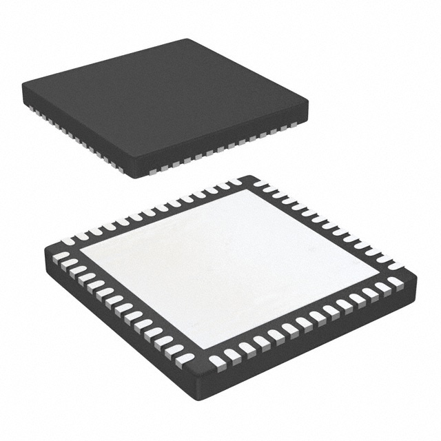


 工商网监
湘ICP备2023018690号
工商网监
湘ICP备2023018690号
