Ultralow Distortion, Low Power, Low Noise, High Speed Op Amp ADA4857-1/ADA4857-2
FEATURES
High speed 850 MHz, −3 dB bandwidth (G = +1, RL = 1 kΩ, LFSCP) 750 MHz, −3 dB bandwidth (G = +1, RL = 1 kΩ, SOIC) 2800 V/μs slew rate Low distortion: −88 dBc @ 10 MHz (G = +1, RL = 1 kΩ) Low power: 5 mA/amplifier @ 10 V Low noise: 4.4 nV/√Hz Wide supply voltage range: 5 V to 10 V Power-down feature Available in 3 mm × 3 mm 8-lead LFCSP (single), 8-lead SOIC (single), and 4 mm × 4 mm 16-lead LFCSP (dual)
CONNECTION DIAGRAMS
ADA4857-1
TOP VIEW (Not to Scale)
PD 1 FB 2 –IN 3 +IN 4 NC = NO CONNECT
8 +VS 7 OUT 6 NC 5 –VS
07040-001
Figure 1. 8-Lead LFCSP (CP)
ADA4857-1
TOP VIEW (Not to Scale) FB 1 –IN 2 +IN 3 –VS 4
8 7 6 5
APPLICATIONS
Instrumentation IF and baseband amplifiers Active filters ADC drivers DAC buffers
PD +VS OUT
07040-002
07040-003
NC
NC = NO CONNECT
Figure 2. 8-Lead SOIC (R)
ADA4857-2
TOP VIEW (Not to Scale)
15 PD1
16 FB1
13 OUT1
12 –VS1 11 NC 10 +IN2 9 –IN2
–IN1 1 +IN1 2 NC 3 –VS2 4
14 +VS1 PD2 7
NC = NO CONNECT
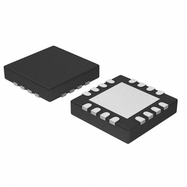
Figure 3. 16-Lead LFCSP (CP)
GENERAL DESCRIPTION
The ADA4857 is a unity gain stable, high speed, voltage feedback amplifier with low distortion, low noise, and high slew rate. With a spurious-free dynamic range (SFDR) of −88 dBc @ 10 MHz, the ADA4857 is an ideal solution in a variety of applications including ultrasounds, ATE, active filters, and ADC drivers. The Analog Devices, Inc., proprietary next-generation XFCB process and innovative architecture enables such high performance amplifiers. The ADA4857 has 850 MHz bandwidth, 2800 V/μs slew rate, and settles to 0.1% in 15 ns. With a wide supply voltage range (5 V to 10 V), the ADA4857 is an ideal candidate for systems that require high dynamic range, precision, and speed. The ADA4857-1 amplifier is available in a 3 mm × 3 mm, 8-lead LFCSP and a standard 8-lead SOIC. The ADA4857-2 is available in a 4 mm × 4 mm, 16-lead LFSCP. The LFCSP features an exposed paddle that provides a low thermal resistance path to the PCB. This path enables more efficient heat transfer and increases reliability. The ADA4857 works over the extended industrial temperature range (−40°C to +125°C).
Rev. 0
Information furnished by Analog Devices is believed to be accurate and reliable. However, no responsibility is assumed by Analog Devices for its use, nor for any infringements of patents or other rights of third parties that may result from its use. Specifications subject to change without notice. No license is granted by implication or otherwise under any patent or patent rights of Analog Devices. Trademarks and registered trademarks are the property of their respective owners.
One Technology Way, P.O. Box 9106, Norwood, MA 02062-9106, U.S.A. Tel: 781.329.4700 www.analog.com Fax: 781.461.3113 ©2008 Analog Devices, Inc. All rights reserved.
OUT2 5
+VS2 6
FB2 8
�ADA4857-1/ADA4857-2 TABLE OF CONTENTS
Features .............................................................................................. 1 Applications....................................................................................... 1 Connection Diagrams...................................................................... 1 General Description ......................................................................... 1 Revision History ............................................................................... 2 Specifications..................................................................................... 3 ±5 V Supply ................................................................................... 3 +5 V Supply ................................................................................... 4 Absolute Maximum Ratings............................................................ 6 Thermal Resistance ...................................................................... 6 Maximum Power Dissipation ..................................................... 6 ESD Caution.................................................................................. 6 Pin Configurations and Function Descriptions ........................... 7 Typical Performance Characteristics ..............................................9 Test Circuits..................................................................................... 15 Applications Information .............................................................. 16 PD Pin Operation....................................................................... 16 Capacitive Load Considerations .............................................. 16 Recommended Values for Various Gains................................ 16 Noise ............................................................................................ 17 Circuit Considerations .............................................................. 17 PCB Layout ................................................................................. 17 Power Supply Bypassing ............................................................ 17 Grounding ................................................................................... 17 Outline Dimensions ....................................................................... 18 Ordering Guide .......................................................................... 19
REVISION HISTORY
5/08—Revision 0: Initial Version
Rev. 0 | Page 2 of 20
�ADA4857-1/ADA4857-2 SPECIFICATIONS
±5 V SUPPLY
TA = 25°C, G = +2, RG = RF = 499 Ω, RL = 1 kΩ to ground, PD = no connect, unless otherwise noted. Table 1.
Parameter DYNAMIC PERFORMANCE –3 dB Bandwidth (LFCSP/SOIC) Conditions G = +1, VOUT = 0.2 V p-p G = +1, VOUT = 2 V p-p G = +2, VOUT = 0.2 V p-p G = +1, VOUT = 2 V p-p, THD < −40 dBc G = +2, VOUT = 2 V p-p, RL = 150 Ω G = +1, VOUT = 4 V step G = +2, VOUT = 2 V step f = 1 MHz, G= +1, VOUT = 2 V p-p (HD2) f = 1 MHz, G= +1, VOUT = 2 V p-p (HD3) f = 10 MHz, G= +1, VOUT = 2 V p-p (HD2) f = 10 MHz, G= +1, VOUT = 2 V p-p (HD3) f = 50 MHz, G= +1, VOUT = 2 V p-p (HD2) f = 50 MHz, G= +1, VOUT = 2 V p-p (HD3) f = 100 kHz f = 100 kHz Min 650 Typ 850/750 600/550 400/350 110 75/90 2800 15 −108 −108 −88 −93 −65 −62 4.4 1.5 ±2 2.3 −2 24.5 50 57 ≥(VCC − 2) ≤(VCC − 4.2) 55 33 58 80 8 4 2 ±4 −86 10 ±4 ±3.7 50 125 10 ±4.5 −3.3 Max Unit MHz MHz MHz MHz MHz V/μs ns dBc dBc dBc dBc dBc dBc nV/√Hz pA/√Hz mV μV/°C μA nA/°C nA dB V V μs ns μA μA MΩ MΩ pF V dB ns V V mA mA pF
Full Power Bandwidth Bandwidth for 0.1 dB Flatness (LFCSP/SOIC) Slew Rate (10% to 90%) Settling Time to 0.1% NOISE/Harmonic PERFORMANCE Harmonic Distortion
Input Voltage Noise Input Current Noise DC PERFORMANCE Input Offset Voltage Input Offset Voltage Drift Input Bias Current Input Bias Current Drift Input Bias Offset Current Open-Loop Gain PD (Power-Down) Pin PD Input Voltage Turn-Off Time Turn-On Time PD Pin Leakage Current INPUT CHARACTERISTICS Input Resistance Input Capacitance Input Common-Mode Voltage Range Common-Mode Rejection Ratio OUTPUT CHARACTERISTICS Output Overdrive Recovery Time Output Voltage Swing Output Current Short-Circuit Current Capacitive Load Drive
VOUT = −2.5 V to +2.5 V Chip powered down Chip enabled 50% off PD to


 工商网监
湘ICP备2023018690号
工商网监
湘ICP备2023018690号
