a
16-/32-Channel, Serially Controlled 4 ⍀
1.8 V to 5.5 V, ⴞ2.5 V, Analog Multiplexers
ADG725/ADG731
FEATURES
3-Wire SPI Compatible Serial Interface
1.8 V to 5.5 V Single Supply
ⴞ2.5 V Dual-Supply Operation
4 ⍀ On Resistance
0.5 ⍀ On Resistance Flatness
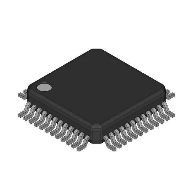
7 mm x 7 mm 48-Lead Chip Scale Package (LFCSP)
or 48-Lead TQFP Package
Rail-to-Rail Operation
Power-On Reset
42 ns Switching Times
Single 32-to-1 Channel Multiplexer
Dual/Differential 16-to-1 Channel Multiplexer
TTL/CMOS Compatible Inputs
For Functionally Equivalent Devices with Parallel
Interface, See ADG726/ADG732
FUNCTIONAL BLOCK DIAGRAM
ADG731
ADG725
S1
S1A
DA
S16A
D
S1B
DB
S32
S16B
INPUT SHIFT
REGISTER
SCLK DIN SYNC
INPUT SHIFT
REGISTER
SCLK DIN SYNC
APPLICATIONS
Optical Applications
Data Acquisition Systems
Communication Systems
Relay Replacement
Audio and Video Switching
Battery-Powered Systems
Medical Instrumentation
Automatic Test Equipment
GENERAL DESCRIPTION
The ADG731/ADG725 are monolithic, CMOS, 32-channel/
dual 16-channel analog multiplexers with a serially controlled
3-wire interface. The ADG731 switches one of 32 inputs
(S1–S32) to a common output, D. The ADG725 can be configured as a dual mux switching one of 16 inputs to one output, or a
differential mux switching one of 16 inputs to a differential output.
These mulitplexers utilize a 3-wire serial interface that is compatible with SPI®, QSPI™, MICROWIRE™, and some DSP
interface standards. On power-up, the Internal Shift Register
contains all zeros and all switches are in the OFF state.
These multiplexers are designed on an enhanced submicron
process that provides low power dissipation yet gives high switching speed with very low on resistance and leakage currents.
They operate from a single supply of 1.8 V to 5.5 V or a
± 2.5 V dual supply, making them ideally suited to a variety of
applications. On resistance is in the region of a few ohms, is
closely matched between switches, and is very flat over the full
signal range.
These parts can operate equally well as either multiplexers or
demultiplexers and have an input signal range that extends to the
supplies. In the OFF condition, signal levels up to the supplies
are blocked. All channels exhibit break-before-make switching
action, preventing momentary shorting when switching channels.
The ADG731 and ADG725 are serially controlled 32-channel,
and dual/differential 16-channel multiplexers, respectively. They
are available in either a 48-lead LFCSP or TQFP package.
PRODUCT HIGHLIGHTS
1.
3-Wire Serial Interface.
2.
1.8 V to 5.5 V Single-Supply or ± 2.5 V Dual-Supply
Operation. These parts are specified and guaranteed
with 5 V ± 10%, 3 V ± 10% single-supply,
and ± 2.5 V ± 10% dual-supply rails.
3.
On Resistance of 4 W.
4.
Guaranteed Break-Before-Make Switching Action.
5.
7 mm ¥ 7 mm 48-Lead Chip Scale Package (LFCSP) or
48-Lead TQFP Package.
REV. A
Information furnished by Analog Devices is believed to be accurate and
reliable. However, no responsibility is assumed by Analog Devices for its
use, nor for any infringements of patents or other rights of third parties that
may result from its use. No license is granted by implication or otherwise
under any patent or patent rights of Analog Devices. Trademarks and
registered trademarks are the property of their respective companies.
One Technology Way, P.O. Box 9106, Norwood, MA 02062-9106, U.S.A.
Tel: 781/329-4700
www.analog.com
Fax: 781/326-8703
© 2003 Analog Devices, Inc. All rights reserved.
�ADG725/ADG731–SPECIFICATIONS1 (V
Parameter
+25⬚C
ANALOG SWITCH
Analog Signal Range
On Resistance (RON)
B Version
–40⬚C to +85⬚C
0 to VDD
4
5.5
On Resistance Match between
Channels (∆RON)
On Resistance Flatness (RFLAT(ON))
6
0.3
0.8
0.5
1
LEAKAGE CURRENTS
Source OFF Leakage IS (OFF)
Drain OFF Leakage ID (OFF)
ADG725
ADG731
Channel ON Leakage ID, IS (ON)
ADG725
ADG731
DIGITAL INPUTS
Input High Voltage, VINH
Input Low Voltage, VINL
Input Current
IINL or IINH
± 0.01
± 0.25
± 0.05
± 0.5
±1
± 0.05
± 0.5
±1
= 5 V ± 10%, VSS = 0 V, GND = 0 V, unless otherwise noted.)
Unit
V
Ω typ
Ω max
Ω typ
Ω max
Ω typ
Ω max
Test Conditions/Comments
VS = 0 V to VDD, IDS = 10 mA;
Test Circuit 1
VS = 0 V to VDD, IDS = 10 mA
VS = 0 V to VDD, IDS = 10 mA
VDD = 5.5 V
VD = 4.5 V/1 V, VS = 1 V/4.5 V;
Test Circuit 2
VD = 4.5 V/1 V, VS = 1 V/4.5 V;
Test Circuit 3
± 2.5
±5
nA typ
nA max
nA typ
nA max
nA max
nA typ
nA max
nA max
2.4
0.8
V min
V max
± 0.5
µA typ
µA max
pF typ
VIN = VINL or VINH
RL = 300 Ω, CL = 35 pF; Test Circuit 5
VS1 = 3 V/0 V, VS32 = 0 V/3 V
RL = 300 Ω, CL = 35 pF
VS = 3 V; Test Circuit 6
VS = 2.5 V, RS = 0 Ω, CL = 1 nF;
Test Circuit 7
RL = 50 Ω, CL = 5 pF, f = 1 MHz;
Test Circuit 8
RL = 50 Ω, CL = 5 pF, f = 1 MHz;
Test Circuit 9
±1
± 2.5
±5
0.005
CIN, Digital Input Capacitance
DD
5
VD = VS = 1 V or 4.5 V;
Test Circuit 4
2
DYNAMIC CHARACTERISTICS
tTRANSITION
Break-Before-Make Time Delay, tD
42
53
30
Charge Injection
5
ns typ
ns max
ns typ
ns min
pC typ
Off Isolation
–72
dB typ
Channel-to-Channel Crosstalk
–72
dB typ
34
18
15
MHz typ
MHz typ
pF typ
RL = 50 Ω, CL = 5 pF; Test Circuit 10
170
340
pF typ
pF typ
f = 1 MHz
f = 1 MHz
175
350
pF typ
pF typ
f = 1 MHz
f = 1 MHz
10
µA typ
µA max
62
1
–3 dB Bandwidth
ADG725
ADG731
CS (OFF)
CD (OFF)
ADG725
ADG731
CD, CS (ON)
ADG725
ADG731
POWER REQUIREMENTS
IDD
20
f = 1 MHz
VDD = 5.5 V
Digital Inputs = 0 V or 5.5 V
NOTES
1
Temperature range is as follows: B Version: –40°C to +85°C.
2
Guaranteed by design, not subject to production test.
Specifications subject to change without notice.
–2–
REV. A
�ADG725/ADG731
SPECIFICATIONS1 (V
DD
Parameter
= 3 V � 10%, VSS = 0 V, GND = 0 V, unless otherwise noted.)
+25⬚C
ANALOG SWITCH
Analog Signal Range
On Resistance (RON)
B Version
–40⬚C to +85⬚C
0 to VDD
7
11
On Resistance Match between
Channels (∆RON)
On Resistance Flatness (RFLAT(ON))
LEAKAGE CURRENTS
Source OFF Leakage IS (OFF)
Drain OFF Leakage ID (OFF)
ADG725
ADG731
Channel ON Leakage ID, IS (ON)
ADG725
ADG731
DIGITAL INPUTS
Input High Voltage, VINH
Input Low Voltage, VINL
Input Current
IINL or IINH
± 0.01
± 0.25
± 0.05
± 0.5
±1
± 0.05
± 0.5
±1
12
0.35
1
3
V
Ω typ
Ω max
Ω typ
Ω max
Ω max
Test Conditions/Comments
VS = 0 V to VDD, IDS = 10 mA;
Test Circuit 1
VS = 0 V to VDD, IDS = 10 mA
VS = 0 V to VDD, IDS = 10 mA
VDD = 3.3 V
VS = 3 V/1 V, VD = 1 V/3 V;
Test Circuit 2
VS = 1 V/3 V, VD = 3 V/1 V;
Test Circuit 3
± 2.5
±5
nA typ
nA max
nA typ
nA max
nA max
nA typ
nA max
nA max
2.0
0.7
V min
V max
± 0.5
µA typ
µA max
pF typ
VIN = VINL or VINH
RL = 300 Ω, CL = 35 pF; Test Circuit 5
VS1 = 2 V/0 V, VS32 = 0 V/2 V
RL = 300 Ω, CL = 35 pF
VS = 2 V; Test Circuit 6
VS = 0 V, RS = 0 Ω, CL = 1 nF;
Test Circuit 7
RL = 50 Ω, CL = 5 pF, f = 1 MHz;
Test Circuit 8
RL = 50 Ω, CL = 5 pF, f = 1 MHz;
Test Circuit 9
±1
± 2.5
±5
0.005
CIN, Digital Input Capacitance
Unit
5
VS = VD = 1 V or 3 V;
Test Circuit 4
2
DYNAMIC CHARACTERISTICS
tTRANSITION
Break-Before-Make Time Delay, tD
60
80
30
Charge Injection
1
ns typ
ns max
ns typ
ns min
pC typ
Off Isolation
–72
dB typ
Channel-to-Channel Crosstalk
–72
dB typ
34
18
15
MHz typ
MHz typ
pF typ
RL = 50 Ω, CL = 5 pF; Test Circuit 10
170
340
pF typ
pF typ
f = 1 MHz
f = 1 MHz
175
350
pF typ
pF typ
f = 1 MHz
f = 1 MHz
5
µA typ
µA max
90
1
–3 dB Bandwidth
ADG725
ADG731
CS (OFF)
CD (OFF)
ADG725
ADG731
CD, CS (ON)
ADG725
ADG731
POWER REQUIREMENTS
IDD
10
NOTES
1
Temperature range is as follows: B Version: –40°C to +85°C.
2
Guaranteed by design, not subject to production test.
Specifications subject to change without notice.
REV. A
–3–
f = 1 MHz
VDD = 3.3 V
Digital Inputs = 0 V or 3.3 V
�ADG725/ADG731
V � 10%, V = –2.5 V � 10%, GND = 0 V,
otherwise noted.)
DUAL-SUPPLY SPECIFICATIONS1 (Vunless= +2.5
DD
Parameter
+25⬚C
ANALOG SWITCH
Analog Signal Range
On Resistance (RON)
B Version
–40⬚C to +85⬚C
VSS to VDD
4
5.5
On Resistance Match Between
Channels (∆RON)
On Resistance Flatness (RFLAT(ON))
6
0.3
0.8
0.5
1
LEAKAGE CURRENTS
Source OFF Leakage IS (OFF)
Drain OFF Leakage ID (OFF)
ADG725
ADG731
Channel ON Leakage ID, IS (ON)
ADG725
ADG731
DIGITAL INPUTS
Input High Voltage, VINH
Input Low Voltage, VINL
Input Current
IINL or IINH
± 0.01
± 0.25
± 0.05
± 0.5
±1
± 0.01
± 0.5
±1
Unit
V
Ω typ
Ω max
Ω typ
Ω max
Ω typ
Ω max
Test Conditions/Comments
VS = VSS to VDD, IDS = 10 mA;
Test Circuit 1
VS = VSS to VDD, IDS = 10 mA
VS = VSS to VDD, IDS = 10 mA
VDD = +2.75 V, VSS = –2.75 V
VS = +2.25 V/–1.25 V, VD = –1.25 V/+2.25 V;
Test Circuit 2
VS = +2.25 V/–1.25 V, VD = –1.25 V/+2.25 V;
Test Circuit 3
± 2.5
±5
nA typ
nA max
nA typ
nA max
nA max
nA typ
nA max
nA max
1.7
0.7
V min
V max
± 0.5
µA typ
µA max
pF typ
VIN = VINL or VINH
RL = 300 Ω, CL = 35 pF; Test Circuit 5
VS1 = 1.5 V/0 V, VS32 = 0 V/1.5 V
RL = 300 Ω, CL = 35 pF
VS = 1.5 V; Test Circuit 6
VS = 0 V, RS = 0 Ω, CL = 1 nF; Test Circuit 7
RL = 50 Ω, CL = 5 pF, f = 1 MHz;
Test Circuit 8
RL = 50 Ω, CL = 5 pF, f = 1 MHz;
Test Circuit 9
± 0.5
± 2.5
±5
0.005
CIN, Digital Input Capacitance
SS
5
VS = VD = +2.25 V/–1.25 V; Test Circuit 4
2
DYNAMIC CHARACTERISTICS
tTRANSITION
Break-Before-Make Time Delay, tD
55
75
15
Charge Injection
Off Isolation
1
–72
ns typ
ns max
ns typ
ns min
pC typ
dB typ
Channel-to-Channel Crosstalk
–72
dB typ
34
18
13
MHz typ
MHz typ
pF typ
RL = 50 Ω, CL = 5 pF; Test Circuit 10
130
260
pF typ
pF typ
f = 1 MHz
f = 1 MHz
150
300
pF typ
pF typ
f = 1 MHz
f = 1 MHz
10
µA typ
µA max
µA typ
µA max
84
1
–3 dB Bandwidth
ADG725
ADG731
CS (OFF)
CD (OFF)
ADG725
ADG731
CD, CS (ON)
ADG725
ADG731
POWER REQUIREMENTS
IDD
20
ISS
10
20
VDD = +2.75 V
Digital Inputs = 0 V or 2.75 V
VSS = –2.75 V
Digital Inputs = 0 V or 2.75 V
NOTES
1
Temperature range is as follows: B Version: –40°C to +85°C.
2
Guaranteed by design, not subject to production test.
Specifications subject to change without notice.
–4–
REV. A
�ADG725/ADG731
TIMING CHARACTERISTICS1, 2
Parameter
Limit at TMIN, TMAX
Unit
Conditions/Comments
fSCLK
t1
t2
t3
t4
t5
t6
t7
t8
30
33
13
13
13
40
5
4.5
33
MHz max
ns min
ns min
ns min
ns min
ns min
ns min
ns min
ns min
SCLK Cycle Frequency
SCLK Cycle Time
SCLK High Time
SCLK Low Time
SYNC to SCLK Falling Edge Setup Time
Minimum SYNC Low Time
Data Setup Time
Data Hold Time
Minimum SYNC High Time
NOTES
1
See Figure 1.
2
All input signals are specified with tr = tf = 5 ns (10% to 90% of V DD) and timed from a voltage level of (V IL + VIH)/2.
Specifications subject to change without notice.
t1
SCLK
t2
t8
t4
t3
t5
SYNC
t7
t6
DB0
DB7
DIN
Figure 1. 3-Wire Serial Interface Timing Diagram
DB0 (LSB)
DB7 (MSB)
EN
CSA CSB
X
A3
A2
A1
EN
DATA BITS
CS
X
A4
A3
A2
A1
A0
DATA BITS
Figure 2. ADG725 Input Shift Register Contents
REV. A
DB0 (LSB)
DB7 (MSB)
A0
Figure 3. ADG731 Input Shift Register Contents
–5–
�ADG725/ADG731
ABSOLUTE MAXIMUM RATINGS 1
Storage Temperature Range . . . . . . . . . . . . –65°C to +150°C
Junction Temperature . . . . . . . . . . . . . . . . . . . . . . . . . . 150°C
Thermal Impedance (4-Layer Board)
48-lead LFCSP . . . . . . . . . . . . . . . . . . . . . . . . . . . 25°C/W
48-lead TQFP . . . . . . . . . . . . . . . . . . . . . . . . . . . 54.6°C/W
Lead Temperature, Soldering (10 seconds) . . . . . . . . . . 300°C
IR Reflow, Peak Temperature (


 工商网监
湘ICP备2023018690号
工商网监
湘ICP备2023018690号
