FEATURES
FUNCTIONAL BLOCK DIAGRAM
ADG904-EP
Wideband switch: –3 dB frequency at 2.5 GHz
Absorptive 4:1 mux/single-pole, four-throw (SP4T)
High off isolation (37 dB at 1 GHz)
Low insertion loss (1.1 dB dc to 1 GHz)
Single 1.65 V to 2.75 V power supply (VDD)
CMOS/LVTTL control logic
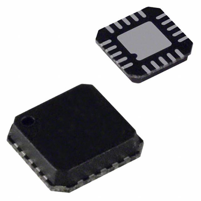
20-lead, 4 mm × 4 mm LFCSP package
Low power consumption (2.5 µA maximum)
RF1
50Ω
RF2
RFC
50Ω
RF3
ENHANCED PRODUCT FEATURES
50Ω
Supports defense and aerospace applications (AQEC standard)
Military temperature range: −55°C to +125°C
Controlled manufacturing baseline
1 assembly/test site
1 fabrication site
Enhanced product change notification
Qualification data available on request
RF4
50Ω
1 OF 4 DECODER
A0
A1
EN
14326-001
Enhanced Product
Wideband 2.5 GHz, 37 dB Isolation at 1 GHz,
CMOS, 1.65 V to 2.75 V, 4:1 Mux/SP4T
ADG904-EP
Figure 1.
APPLICATIONS
Wireless communications
General-purpose radio frequency (RF) switching
Dual-band applications
High speed filter selection
Digital transceiver front-end switches
IF switching
Tuner modules
Antenna diversity switching
GENERAL DESCRIPTION
The ADG904-EP is a wideband analog 4:1 multiplexer that uses
a CMOS process to provide high isolation and low insertion
loss to 1 GHz. The ADG904-EP is an absorptive/matched mux
with 50 Ω terminated shunt legs. This device is designed such
that the isolation is high over the dc to 1 GHz frequency range.
The device has on-board CMOS control logic, which eliminates
the need for external control circuitry. The control inputs are both
CMOS and LVTTL compatible. The low power consumption of
this device makes it ideally suited for wireless applications and
general-purpose high frequency switching.
The ADG904-EP switches one of four inputs to a common
output, RFC, as determined by the 3-bit binary address lines
A0, A1, and EN. A Logic 1 on the EN pin disables the device.
Additional application and technical information can be found
in the ADG904 data sheet.
PRODUCT HIGHLIGHTS
1.
2.
3.
Rev. C
37 dB off isolation at 1 GHz.
1.1 dB insertion loss at 1 GHz.
20-lead LFCSP package.
Document Feedback
Information furnished by Analog Devices is believed to be accurate and reliable. However, no
responsibility is assumed by Analog Devices for its use, nor for any infringements of patents or other
rights of third parties that may result from its use. Specifications subject to change without notice. No
license is granted by implication or otherwise under any patent or patent rights of Analog Devices.
Trademarks and registered trademarks are the property of their respective owners.
One Technology Way, P.O. Box 9106, Norwood, MA 02062-9106, U.S.A.
Tel: 781.329.4700 ©2016–2017 Analog Devices, Inc. All rights reserved.
Technical Support
www.analog.com
�ADG904-EP
Enhanced Product
TABLE OF CONTENTS
Features .............................................................................................. 1
Absolute Maximum Ratings ............................................................5
Enhanced Product Features ............................................................ 1
Thermal Resistance .......................................................................5
Applications ....................................................................................... 1
ESD Caution...................................................................................5
Functional Block Diagram .............................................................. 1
Pin Configuration and Function Descriptions..............................6
General Description ......................................................................... 1
Typical Performance Characteristics ..............................................7
Product Highlights ........................................................................... 1
Test Circuits........................................................................................9
Revision History ............................................................................... 2
Outline Dimensions ....................................................................... 11
Specifications..................................................................................... 3
Ordering Guide .......................................................................... 11
Continous Current Per Channel ................................................ 4
REVISION HISTORY
5/2017—Rev. B to Rev. C
Change to Endnote 1, Table 3 ......................................................... 3
Updated Outline Dimensions ....................................................... 11
3/2017—Rev. A to Rev. B
Changes to Endnote 4, Table 1 ........................................................ 3
Added Endnote 1, Table 2................................................................ 4
11/2016—Rev. 0 to Rev. A
Changes to Figure 15 ........................................................................ 9
6/2016—Revision 0: Initial Version
Rev. C | Page 2 of 11
�Enhanced Product
ADG904-EP
SPECIFICATIONS
VDD = 1.65 V to 2.75 V, GND = 0 V, input power = 0 dBm, temperature range = −55°C to +125°C, unless otherwise noted.
Table 1.
Parameter
AC ELECTRICAL CHARACTERISTICS
−3 dB Frequency 2
Insertion Loss
Symbol
Test Conditions/Comments
S12, S21
DC to 100 MHz; VDD = 2.5 V ± 10%;
see Figure 18
500 MHz; VDD = 2.5 V ± 10%
1000 MHz; VDD = 2.5 V ± 10%
100 MHz; see Figure 17
500 MHz; see Figure 17
1000 MHz; see Figure 17
100 MHz; see Figure 19
500 MHz; see Figure 19
1000 MHz; see Figure 19
Isolation—RFC to RF1x
S12, S21
Crosstalk
S12, S21
Return Loss2
On Channel
S11, S22
DC to 100 MHz
500 MHz
1000 MHz
DC to 100 MHz
500 MHz
1000 MHz
Off Channel
Timing
On Switching Time2
Off Switching Time
2
Transition Time
Rise Time2
Fall Time2
Third-Order Intermodulation Intercept
Video Feedthrough 3
INPUT POWER
1 dB Input Compression
DC ELECTRICAL CHARACTERISTICS
Input High Voltage
Input Low Voltage
Input Leakage Current
CAPACITANCE2
RF Port On Capacitance
Digital Input Capacitance
POWER REQUIREMENTS
VDD
Quiescent Power Supply Current
Min
51
35
30
50
32
30
19
14
Typ 1
Max
Unit
2.5
0.5
1
GHz
dB
0.7
1.1
60
45
37
58
35
35
1.2
1.8
27
26
18
22
19
18
dB
dB
dB
dB
dB
dB
dB
dB
dB
dB
dB
dB
dB
dB
tON (EN)
50% EN to 90% RF; see Figure 15
8.5
10
ns
tOFF (EN)
50% EN to 10% RF; see Figure 15
13
16
ns
tTRANS
tRISE
tFALL
IP3
50% A0/A1 to 10% RF
10% to 90% RF; see Figure 16
90% to 10% RF; see Figure 16
900 MHz/901 MHz, 4 dBm; see Figure 21
See Figure 20
12
3
7.5
31
3
15
5
11
ns
ns
ns
dBm
mV p-p
P1dB
1000 MHz 4; see Figure 22
VINH
VDD = 2.25 V to 2.75 V
VDD = 1.65 V to 1.95 V
VDD = 2.25 V to 2.75 V
VDD = 1.65 V to 1.95 V
0 V ≤ VIN ≤ 2.75 V
f = 1 MHz
VINL
II
25
16
dBm
±0.1
V
V
V
V
µA
1.7
0.65 VDD
CRF ON
C
3
2
1.65
IDD
0.7
0.35 VDD
±1
Digital inputs = 0 V or VDD
0.1
pF
pF
2.75
2.5
V
µA
Typical values are at VDD = 2.5 V and 25°C, unless otherwise stated.
Guaranteed by design, not subject to production test.
3
Video feedthrough is the dc transience at the output of any port of the switch when the control voltage is switched from high to low or low to high in a 50 Ω test
setup, measured with 1 ns rise time pulses and 500 MHz bandwidth.
4
Less than 100 MHz, refer to the AN-952 Application Note for more information about power handling.
1
2
Rev. C | Page 3 of 11
�ADG904-EP
Enhanced Product
CONTINOUS CURRENT PER CHANNEL
Table 2.
Parameter
CONTINUOUS CURRENT PER
CHANNEL1
VDD = 2.75 V, VSS = 0 V
VDD = 1.65 V, VSS = 0 V
1
25°C
85°C
105°C
125°C
Unit
93.1
82.6
10.8
10.8
5.9
5.9
3.3
3.3
mA maximum
mA maximum
Guaranteed by design, not production tested.
Rev. C | Page 4 of 11
Test Conditions/Comments
20-lead LFCSP, θJA = 30.4°C/W, dc bias = 0.5 V
�Enhanced Product
ADG904-EP
ABSOLUTE MAXIMUM RATINGS
TA = 25°C, unless otherwise noted.
THERMAL RESISTANCE
Table 3.
Thermal performance is directly linked to printed circuit board
(PCB) design and operating environment. Careful attention to
PCB thermal design is required.
Parameter
VDD to GND1
Inputs to GND1
Continuous Current
Input Power4
Operating Temperature Range (Industrial)
Storage Temperature Range
Junction Temperature
Lead Temperature, Soldering (10 sec)
IR Reflow, Peak Temperature ( 2.2 V (RFx to RFC)
–0.2
–0.3
–0.4
–0.5
–0.6
–0.7
TA = –40°C
–0.8
TA = +25°C
–0.9
–1.0
–1.1
–1.2
–1.3
–1.4
–1.5
–1.6
–1.7
–1.8
–1.9
–2.0
–2.1
–2.2
–2.3
–2.4
–2.5
–2.6
–2.7
–2.8
–2.9
–3.0
10k
100k
1M
TA = –55°C
TA = +85°C
TA = +125°C
10M
100M
1G
10G
FREQUENCY (Hz)
14326-006
VDD = 2.25V
INSERTION LOSS (dB)
–0.3
–0.4
–0.5
–0.6
–0.7
–0.8
–0.9
–1.0
–1.1
–1.2
–1.3
–1.4
–1.5
–1.6
–1.7
–1.8
–1.9
–2.0
–2.1
–2.2
–2.3
–2.4
–2.5
–2.6
–2.7
–2.8
–2.9 TA = 25°C
–3.0
10k
100k
14326-015
INSERTION LOSS (dB)
TYPICAL PERFORMANCE CHARACTERISTICS
Figure 6. Insertion Loss vs. Frequency over Various Temperature (RFx to RFC)
–0.3
–10
–0.4
–20
VDD = 1.65V TO 2.75V
–30
VDD = 2.50V
–40
–0.6
ISOLATION (dB)
VDD = 2.75V
–0.7
VDD = 2.25V
–0.8
–50
S21
–60
–70
S12
–0.9
–80
–1.0
100k
1M
10M
100M
FREQUENCY (Hz)
1G
10G
–100
10k
10M
100M
FREQUENCY (Hz)
1G
10G
–10
–20
VDD = 1.65V
–30
ISOLATION (dB)
–0.3
–0.4
–0.5
–0.6
–0.7
–0.8
–0.9
–1.0
–1.1
–1.2
–1.3
–1.4
–1.5
–1.6
–1.7
–1.8
–1.9
–2.0
–2.1
–2.2
–2.3
–2.4
–2.5
–2.6
–2.7
–2.8
–2.9 TA = 25°C
–3.0
10k
100k
1M
Figure 7. Isolation vs. Frequency over Supplies (RFx to RFC)
VDD = 1.80V
VDD = 1.95V
TA = +125°C
TA = +85°C
–40
–50
TA = +25°C
–60
TA = –40°C
–70
–80
–90
TA = –55°C
1M
10M
100M
FREQUENCY (Hz)
1G
10G
Figure 5. Insertion Loss vs. Frequency for VDD < 2 V (RFx to RFC)
14326-013
INSERTION LOSS (dB)
Figure 4. Insertion Loss vs. Frequency for VDD > 2.2 V (RFx to RFC)
Zoomed View of Figure 3
100k
14326-017
–1.1
10k
14326-014
–90
TA = 25°C
–100
10k
100k
1M
10M
100M
FREQUENCY (Hz)
1G
10G
14326-008
INSERTION LOSS (dB)
–0.5
Figure 8. Isolation vs. Frequency over Various Temperature (RFx to RFC)
Rev. C | Page 7 of 11
�ADG904-EP
Enhanced Product
0
[T]
TRIG'D
Δ: 2.40mV
T
–5
A0
RETURN LOSS (dB)
–10
–15
1
–20
OFF SWITCH
3
–25
RFC
ON SWITCH
1M
10M
100M
FREQUENCY (Hz)
1G
10G
CH1 1.00V
CH3 1.00mV
M 20.0ns
Figure 12. Video Feedthrough
Figure 9. Return Loss vs. Frequency (RFx to RFC)
–10
35
–20
30
–30
25
–40
20
IP3 (dB)
–50
15
10
–60
5
–70
VDD = 2.5V
TA = 25°C
1M
10M
100M
FREQUENCY (Hz)
1G
10G
0
100
200
300
400
500
600
FREQUENCY (MHz)
700
800
900
14326-019
100k
14326-025
–80
10k
VDD = 2.5V
TA = 25°C
Figure 13. Third-Order Intermodulation Intercept (IP3) vs. Frequency
Figure 10. Crosstalk vs. Frequency
18
TEK RUN: 5.00GSPS ET ENVELOPE
[
T
]
16
1dB INPUT COMPRESSION (dBm)
A1
1
3
RF1/3
14
12
10
8
6
4
2
VDD = 2.5V
TA = 25°C
0
1.00V
100mV
CH2
100mV
M 5.00ns
0
14326-026
CH1
CH3
250
500
750
1000
FREQUENCY (MHz)
1250
1500
14326-002
CROSSTALK (dB)
14326-027
VDD = 2.5V
TA = 25°C
–35
10k
100k
14326-020
–30
Figure 14. 1 dB Input Compression vs. Frequency (DC Bias Not Used)
Figure 11. Switch Timing
Rev. C | Page 8 of 11
�Enhanced Product
ADG904-EP
TEST CIRCUITS
VDD
10µF
VDD
VDD
RFx
VDD
RFC
90%
VOUT
GND
50%
10%
tON
tOFF
NETWORK
ANALYZER
50Ω
RF2
A0
A1
50Ω
VS
50Ω
1 OF 4
DECODER
14326-104
VEN
RL
50Ω
EN
50%
VOUT
50Ω
VOUT
RFx
RFC
VS
RL
50Ω
ADG904-EP
GND
EN
INSERTION LOSS = 20log
14326-107
10µF
VOUT
VS
Figure 18. Insertion Loss
Figure 15. Switch Timing, tON (EN) and tOFF (EN)
VDD
10µF
VDD
VDD
RF1
VDD
VOUT
Ax
50%
50%
VOUT
50Ω
RF2
90%
10%
90%
10%
1 OF 4
DECODER
14326-105
GND
tRISE
tFALL
A0
A1
RL
50Ω
VOUT
50Ω
GND
EN
CROSSTALK = 20log
VOUT
VS
Figure 19. Crosstalk
Figure 16. Switch Timing, tRISE and tFALL
VDD
VDD
10µF
10µF
VDD
50Ω
ADG904-EP
RF1
RFC
RL
50Ω
VS
VDD
RFx
OSCILLOSCOPE
RF2
A1
EN
RFC
RF2
50Ω
1 OF 4
DECODER
GND
V
OFF ISOLATION = 20log OUT
VS
A0
A1
EN
Figure 20. Video Feedthrough
Figure 17. Off Isolation
Rev. C | Page 9 of 11
NC
50Ω
NETWORK
ANALYZER
14326-106
1 OF 4
DECODER
50Ω
ADG904-EP
VOUT
50Ω
A0
VS
50Ω
VAx
RL
50Ω
50Ω
NC
50Ω
GND
14326-109
VS
RFC
RFx
RFC
NETWORK
ANALYZER
ADG904-EP
14326-108
10µF
�ADG904-EP
Enhanced Product
VDD
VDD
10µF
ADG904-EP
VDD
RF1
SPECTRUM RFC
ANALYZER
50Ω
50Ω
RF2
1 OF 4
DECODER
50Ω
A1
SPECTRUM
ANALYZER
RFC
RF2
RF
SOURCE
EN
1 OF 4
DECODER
Figure 21. Third-Order Intermodulation Intercept (IP3)
50Ω
50Ω
COMBINER
GND
A0
ADG904-EP
RF1
RF
SOURCE
14326-110
VDD
RF
SOURCE
GND
A0
A1
EN
Figure 22. 1 dB Input Compression (P1dB)
Rev. C | Page 10 of 11
VS
50Ω
14326-111
10µF
�Enhanced Product
ADG904-EP
OUTLINE DIMENSIONS
PIN 1
INDICATOR
DETAIL A
(JEDEC 95)
4.10
4.00 SQ
3.90
0.30
0.25
0.18
0.50
BSC
PIN 1
INDIC ATOR AREA OPTIONS
(SEE DETAIL A)
20
16
15
1
2.30
2.10 SQ
2.00
EXPOSED
PAD
5
11
10
6
BOTTOM VIEW
0.20 MIN
FOR PROPER CONNECTION OF
THE EXPOSED PAD, REFER TO
THE PIN CONFIGURATION AND
0.05 MAX
FUNCTION DESCRIPTIONS
0.02 NOM
SECTION OF THIS DATA SHEET.
COPLANARITY
0.08
0.203 REF
0.80
0.75
0.70
SEATING
PLANE
PKG-003763
0.65
0.60
0.55
COMPLIANT TO JEDEC STANDARDS MO-220-WGGD-1
02-13-2017-B
TOP VIEW
Figure 23. 20-Lead Lead Frame Chip Scale Package [LFCSP]
4 mm × 4 mm Body and 0.75 mm Package Height
(CP-20-6)
Dimensions shown in millimeters
ORDERING GUIDE
Model 1
ADG904SCPZ-EP
ADG904SCPZ-EP-RL7
1
Temperature Range
−55°C to +125°C
−55°C to +125°C
Package Description
20-Lead Lead Frame Chip Scale Package [LFCSP]
20-Lead Lead Frame Chip Scale Package [LFCSP]
Z = RoHS Compliant Part.
©2016–2017 Analog Devices, Inc. All rights reserved. Trademarks and
registered trademarks are the property of their respective owners.
D14326-0-5/17(C)
Rev. C | Page 11 of 11
Package Option
CP-20-6
CP-20-6
�


 工商网监
湘ICP备2023018690号
工商网监
湘ICP备2023018690号
