30 MHz to 6 GHz
RF/IF Gain Block
ADL5610
Data Sheet
FUNCTIONAL BLOCK DIAGRAM
Fixed gain of 18.4 dB
Broad operation from 30 MHz to 6 GHz
High dynamic range gain block
Input and output internally matched to 50 Ω
Integrated bias circuit
OIP3 of 38.8 dBm at 900 MHz
P1dB of 20.4 dBm at 900 MHz
Noise figure of 2.2 dB at 900 MHz
Single 5 V power supply
Low quiescent current of 92 mA
Wide operating temperature range of −40°C to +105°C
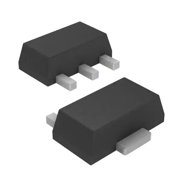
Thermally efficient SOT-89 package
ESD rating of ±1.5 kV (Class 1C)
GND
(2)
ADL5610
BIAS
1
2
3
RFIN
GND
RFOUT
11507-001
FEATURES
Figure 1.
GENERAL DESCRIPTION
The ADL5610 is a single-ended RF/IF gain block amplifier that
provides broadband operation from 30 MHz to 6 GHz. The
ADL5610 provides a low noise figure of 2.2 dB with a very high
OIP3 of more than 38 dBm simultaneously, which delivers a
high dynamic range.
The ADL5610 provides a gain of 18 dB, which is stable over
frequency, temperature, and power supply, and from device to
device. The amplifier is offered in the industry-standard SOT-89
package and is internally matched to 50 Ω at the input and
Rev. B
output, making the ADL5610 easy to implement in a wide
variety of applications. The only external parts required are the
input and output ac coupling capacitors, power supply decoupling
capacitors, and bias inductor.
The ADL5610 has a high ESD rating of ±1.5 kV (Class 1C) and
is fully specified for operation across a wide temperature range
of −40°C to +105°C.
A fully populated RoHS-compliant evaluation board is available.
Document Feedback
Information furnished by Analog Devices is believed to be accurate and reliable. However, no
responsibility is assumed by Analog Devices for its use, nor for any infringements of patents or other
rights of third parties that may result from its use. Specifications subject to change without notice. No
license is granted by implication or otherwise under any patent or patent rights of Analog Devices.
Trademarks and registered trademarks are the property of their respective owners.
One Technology Way, P.O. Box 9106, Norwood, MA 02062-9106, U.S.A.
Tel: 781.329.4700 ©2013–2015 Analog Devices, Inc. All rights reserved.
Technical Support
www.analog.com
�ADL5610
Data Sheet
TABLE OF CONTENTS
Features .............................................................................................. 1
500 MHz to 6 GHz Frequency Band ..........................................9
Functional Block Diagram .............................................................. 1
30 MHz to 500 MHz Frequency Band..................................... 10
General Description ......................................................................... 1
General......................................................................................... 11
Revision History ............................................................................... 2
Applications Information .............................................................. 13
Specifications..................................................................................... 3
Basic Connections ...................................................................... 13
Typical Scattering Parameters (S-Parameters) ......................... 5
Absolute Maximum Ratings ............................................................ 7
Soldering Information and Recommended PCB
Land Pattern ................................................................................ 14
Thermal Resistance ...................................................................... 7
W-CDMA ACPR Performance ................................................ 14
ESD Caution .................................................................................. 7
Evaluation Board ............................................................................ 15
Pin Configuration and Function Descriptions ............................. 8
Outline Dimensions ....................................................................... 16
Typical Performance Characteristics ............................................. 9
Ordering Guide .......................................................................... 16
REVISION HISTORY
12/15—Rev. A to Rev. B
Updated Outline Dimensions ....................................................... 16
9/13—Rev. 0 to Rev. A
Added Figure 19; Renumbered Sequentially .............................. 11
Changes to Figure 29 ...................................................................... 14
Updated Outline Dimensions ....................................................... 16
7/13—Revision 0: Initial Version
Rev. B | Page 2 of 16
�Data Sheet
ADL5610
SPECIFICATIONS
VPOS = 5 V and TA = 25°C, unless otherwise noted.
Table 1.
Parameter
OVERALL FUNCTION
Frequency Range
FREQUENCY = 30 MHz
Gain
Output 1 dB Compression Point (P1dB)
Output Third-Order Intercept (OIP3)
Noise Figure1
FREQUENCY = 140 MHz
Gain
vs. Frequency
vs. Temperature
vs. Supply
Output 1 dB Compression Point
Output Third-Order Intercept
Noise Figure1
FREQUENCY = 350 MHz
Gain
vs. Frequency
vs. Temperature
vs. Supply
Output 1 dB Compression Point
Output Third-Order Intercept
Noise Figure1
FREQUENCY = 700 MHz
Gain
vs. Frequency
vs. Temperature
vs. Supply
Output 1 dB Compression Point
Output Third-Order Intercept
Noise Figure1
FREQUENCY = 900 MHz
Gain
vs. Frequency
vs. Temperature
vs. Supply
Output 1 dB Compression Point
Output Third-Order Intercept
Noise Figure
FREQUENCY = 1900 MHz
Gain
vs. Frequency
vs. Temperature
vs. Supply
Output 1 dB Compression Point
Output Third-Order Intercept
Noise Figure1
Test Conditions/Comments
Min
Typ
30
Δf = 1 MHz, output power (POUT) = 3 dBm per tone
±10 MHz
−40°C ≤ TA ≤ +105°C
4.75 V to 5.25 V
Δf = 1 MHz, POUT = 3 dBm per tone
±10 MHz
−40°C ≤ TA ≤ +105°C
4.75 V to 5.25 V
Δf = 1 MHz, output power (POUT) = 3 dBm per tone
±50 MHz
−40°C ≤ TA ≤ +105°C
4.75 V to 5.25 V
Δf = 1 MHz, POUT = 3 dBm per tone
Rev. B | Page 3 of 16
6000
MHz
18.1
16.1
30.8
2.8
dB
dBm
dBm
dB
15.0
±0.43
±0.33
±0.04
16.0
29.3
2.6
dB
dB
dB
dB
dBm
dBm
dB
18.1
±0.04
±0.29
±0.02
20.2
34.6
2.1
dB
dB
dB
dB
dBm
dBm
dB
18.4
±0.02
±0.23
±0.04
20.4
38.4
2.2
dB
dB
dB
dB
dBm
dBm
dB
18.4
±0.01
±0.22
±0.05
20.4
38.8
2.2
19.4
dB
dB
dB
dB
dBm
dBm
dB
16.9
17.9
±0.05
±0.23
±0.11
20.1
38.7
2.5
18.9
dB
dB
dB
dB
dBm
dBm
dB
Δf = 1 MHz, POUT = 3 dBm per tone
Δf = 1 MHz, POUT = 3 dBm per tone
Unit
17.4
±50 MHz
−40°C ≤ TA ≤ +105°C
4.75 V to 5.25 V
±50 MHz
−40°C ≤ TA ≤ +105°C
4.75 V to 5.25 V
Max
�ADL5610
Parameter
FREQUENCY = 2140 MHz
Gain
vs. Frequency
vs. Temperature
vs. Supply
Output 1 dB Compression Point
Output Third-Order Intercept
Noise Figure1
FREQUENCY = 2600 MHz
Gain
vs. Frequency
vs. Temperature
vs. Supply
Output 1 dB Compression Point
Output Third-Order Intercept
Noise Figure1
FREQUENCY = 3500 MHz
Gain
vs. Frequency
vs. Temperature
vs. Supply
Output 1 dB Compression Point
Output Third-Order Intercept
Noise Figure1
FREQUENCY = 4000 MHz
Gain
vs. Frequency
vs. Temperature
vs. Supply
Output 1 dB Compression Point
Output Third-Order Intercept
Noise Figure1
FREQUENCY = 5000 MHz
Gain
vs. Frequency
vs. Temperature
vs. Supply
Output 1 dB Compression Point
Output Third-Order Intercept
Noise Figure
FREQUENCY = 5800 MHz
Gain
vs. Frequency
vs. Temperature
vs. Supply
Output 1 dB Compression Point
Output Third-Order Intercept
Noise Figure1
Data Sheet
Test Conditions/Comments
±50 MHz
−40°C ≤ TA ≤ +105°C
4.75 V to 5.25 V
Δf = 1 MHz, POUT = 3 dBm per tone
±50 MHz
−40°C ≤ TA ≤ +105°C
4.75 V to 5.25 V
Δf = 1 MHz, POUT = 3 dBm per tone
±50 MHz
−40°C ≤ TA ≤ +105°C
4.75 V to 5.25 V
Δf = 1 MHz, POUT = 3 dBm per tone
±50 MHz
−40°C ≤ TA ≤ +105°C
4.75 V to 5.25 V
Δf = 1 MHz, POUT = 3 dBm per tone
±50 MHz
−40°C ≤ TA ≤ +105°C
4.75 V to 5.25 V
Δf = 1 MHz, POUT = 3 dBm per tone
±50 MHz
−40°C ≤ TA ≤ +105°C
4.75 V to 5.25 V
Δf = 1 MHz, POUT = 3 dBm per tone
Rev. B | Page 4 of 16
Min
Typ
Max
Unit
17.8
±0.03
±0.25
±0.13
19.9
36.8
2.7
dB
dB
dB
dB
dBm
dBm
dB
17.5
±0.03
±0.28
±0.15
18.7
33.5
2.8
dB
dB
dB
dB
dBm
dBm
dB
17.6
±0.04
±0.45
±0.19
17.4
29.4
3.0
dB
dB
dB
dB
dBm
dBm
dB
17.9
±0.04
±0.84
±0.24
16.4
27.6
3.2
dB
dB
dB
dB
dBm
dBm
dB
15.3
±0.11
±1.27
±0.33
15.7
26.1
4.4
dB
dB
dB
dB
dBm
dBm
dB
13.2
±0.08
±1.36
±0.33
12.5
21.2
6.1
dB
dB
dB
dB
dBm
dBm
dB
�Data Sheet
ADL5610
Parameter
POWER INTERFACE
Supply Voltage
Supply Current
vs. Temperature
Power Dissipation
1
Test Conditions/Comments
Min
Typ
Max
Unit
VPOS
4.75
5
92
−6/+14
460
5.25
118
V
mA
mA
mW
−40°C ≤ TA ≤ +105°C
Noise figure specified includes printed circuit board (PCB) traces losses.
TYPICAL SCATTERING PARAMETERS (S-PARAMETERS)
VPOS = 5 V and TA = 25°C.
Table 2.
Frequency
(MHz)
30
50
100
200
300
400
500
600
700
800
900
1000
1100
1200
1300
1400
1500
1600
1700
1800
1900
2000
2100
2200
2300
2400
2500
2600
2700
2800
2900
3000
3100
3200
3300
3400
3500
S11
Magnitude (dB)
−19.575
−13.194
−8.023
−10.635
−13.978
−16.890
−14.057
−15.303
−17.025
−18.532
−19.926
−21.266
−22.659
−24.210
−26.057
−28.536
−31.933
−34.750
−32.172
−27.781
−24.468
−21.613
−19.342
−17.343
−15.863
−14.592
−13.521
−12.680
−11.965
−11.364
−10.983
−10.683
−10.470
−10.377
−10.454
−10.733
−11.222
Angle (°)
−21.758
+17.280
−17.286
−67.774
−93.402
−111.950
−140.270
−160.894
−180.268
−198.771
−216.383
−233.373
−248.512
−262.937
−274.666
−282.527
−279.454
−255.300
−220.241
−211.620
−218.185
−222.836
−232.483
−243.288
−253.959
−264.759
−275.854
−286.432
−296.744
−307.385
−318.098
−328.063
−338.914
−349.594
−360.106
−371.185
−381.299
S21
Magnitude (dB)
18.186
+16.748
+13.552
+16.801
+17.960
+18.355
+18.204
+18.339
+18.416
+18.434
+18.425
+18.401
+18.366
+18.320
+18.272
+18.220
+18.166
+18.106
+18.046
+17.977
+17.916
+17.843
+17.783
+17.740
+17.682
+17.629
+17.583
+17.533
+17.494
+17.466
+17.441
+17.448
+17.468
+17.503
+17.556
+17.609
+17.683
Angle (°)
+167.401
+158.342
+168.911
+171.154
+154.322
+138.243
−229.198
−243.615
−258.515
−272.822
−286.779
−300.434
−313.941
−327.244
−340.437
−353.552
−366.576
−379.548
−392.387
−405.225
−418.174
−430.638
−443.294
−455.878
−468.509
−481.088
−493.684
−506.169
−518.608
−531.068
−543.539
−555.886
−568.495
−581.114
−593.755
−606.730
−619.682
Rev. B | Page 5 of 16
S12
Magnitude (dB)
−23.536
−24.873
−27.865
−24.787
−23.679
−23.336
−23.467
−23.322
−23.214
−23.143
−23.102
−23.099
−23.071
−23.068
−23.063
−23.065
−23.063
−23.067
−23.070
−23.085
−23.047
−23.111
−23.127
−23.141
−23.139
−23.129
−23.123
−23.114
−23.122
−23.105
−23.013
−22.967
−22.910
−22.848
−22.757
−22.674
−22.581
Angle (°)
+0.034
−11.954
−5.368
−2.040
−16.582
−29.568
−33.884
−45.046
−56.945
−68.374
−79.290
−90.132
−100.705
−111.189
−121.632
−131.946
−142.239
−152.499
−162.725
−173.046
−183.266
−193.454
−203.629
−213.605
−223.746
−233.823
−243.825
−254.026
−264.148
−274.109
−284.190
−294.664
−304.790
−315.180
−325.637
−336.157
−346.908
S22
Magnitude (dB)
−12.040
−8.336
−5.677
−8.176
−10.953
−12.818
−10.083
−10.629
−11.317
−11.700
−11.891
−11.967
−11.951
−11.897
−11.812
−11.702
−11.599
−11.467
−11.381
−11.275
−11.132
−11.136
−11.017
−10.826
−10.670
−10.488
−10.295
−10.160
−10.022
−9.909
−9.885
−9.958
−10.016
−10.207
−10.506
−10.842
−11.291
Angle (°)
−154.592
−158.609
−189.790
−225.737
−237.962
−242.287
+104.308
+98.947
+95.056
+91.300
+87.191
+82.648
+77.917
+72.400
+66.929
+61.131
+55.505
+49.533
+43.914
+38.152
+32.216
+27.227
+21.933
+16.768
+10.889
+4.907
−1.461
−8.539
−15.582
−23.543
−32.338
−41.038
−50.760
−61.042
−72.485
−85.064
−98.903
�ADL5610
Frequency
(MHz)
3600
3700
3800
3900
4000
4100
4200
4300
4440
4500
4600
4700
4800
4900
5000
5100
5200
5300
5400
5500
5600
5700
5800
5900
6000
S11
Magnitude (dB)
−11.851
−12.849
−14.417
−16.531
−19.249
−24.999
−32.089
−21.011
−14.797
−10.740
−8.451
−7.237
−6.447
−5.907
−5.507
−5.147
−4.964
−4.929
−4.758
−4.735
−4.686
−4.708
−4.782
−4.821
−4.831
Data Sheet
Angle (°)
−392.155
−403.342
−413.805
−425.971
−436.011
−460.302
−556.369
−617.527
−639.680
−661.435
−681.844
−698.863
−713.011
−724.933
−735.570
−745.147
−754.155
−762.147
−770.468
−779.351
−786.735
−793.953
−800.356
−807.419
−812.689
S21
Magnitude (dB)
+17.768
+17.830
+17.904
+17.938
+18.010
+17.915
+17.769
+17.448
+16.876
+16.212
+15.849
+15.707
+15.581
+15.413
+15.210
+14.998
+14.767
+14.507
+14.376
+14.216
+14.109
+13.986
+13.873
+13.750
+13.663
Angle (°)
−633.032
−646.607
−660.333
−674.447
−689.430
−704.472
−719.835
−735.470
−750.505
−763.011
−773.947
−785.709
−798.441
−811.388
−824.332
−837.253
−850.018
−862.399
−874.651
−887.558
−900.141
−913.048
−925.986
−939.485
−952.755
Rev. B | Page 6 of 16
S12
Magnitude (dB)
−22.457
−22.372
−22.234
−22.200
−22.085
−22.195
−22.338
−22.655
−23.014
−23.353
−23.431
−23.418
−23.453
−23.569
−23.748
−23.929
−23.998
−24.155
−24.220
−24.481
−24.355
−24.406
−24.277
−24.360
−24.108
Angle (°)
−358.060
−369.044
−380.712
−392.377
−405.026
−417.459
−430.127
−442.759
−453.711
−463.267
−472.943
−483.451
−494.525
−505.774
−516.626
−527.665
−538.788
−548.537
−559.477
−568.644
−579.878
−589.889
−599.855
−611.222
−622.580
S22
Magnitude (dB)
−11.908
−12.522
−13.184
−13.538
−13.882
−13.296
−12.342
−11.165
−9.840
−8.338
−7.134
−6.336
−5.808
−5.457
−5.207
−5.106
−5.099
−5.180
−5.313
−5.672
−6.142
−6.809
−7.749
−8.867
−10.361
Angle (°)
−114.642
−132.684
−153.495
−177.923
−202.196
−228.659
−252.450
−273.722
−292.336
−310.540
−329.131
−346.718
−362.618
−377.358
−391.101
−404.171
−416.123
−428.050
−440.141
−453.016
−464.297
−476.641
−488.815
−501.594
−513.719
�Data Sheet
ADL5610
ABSOLUTE MAXIMUM RATINGS
THERMAL RESISTANCE
Table 3.
Parameter
Supply Voltage, VPOS
Input Power (50 Ω Impedance)
Internal Power Dissipation (Pad Soldered to
Ground)
ESD Human Body Model (HBM) Rating (ESDA/
JEDEC JS-001-2011)
Maximum Junction Temperature
Operating Temperature Range
Storage Temperature Range
Table 4 lists the junction-to-air thermal resistance (θJA) and the
junction-to-case thermal resistance (θJC) for the ADL5610.
Rating
6.5 V
20 dBm
800 mW
Table 4. Thermal Resistance
Package Type
3-Lead SOT-89 (RK-3)
±1.5 kV
Stresses at or above those listed under Absolute Maximum
Ratings may cause permanent damage to the product. This is a
stress rating only; functional operation of the product at these
or any other conditions above those indicated in the operational
section of this specification is not implied. Operation beyond
the maximum operating conditions for extended periods may
affect product reliability.
θJC2
9
Unit
°C/W
Measured on the ADL5610 evaluation board. For more information about
board layout, see the Soldering Information and Recommended PCB Land
Pattern section.
2
Based on simulation with a standard JEDEC board per JESD51.
1
150°C
−40°C to +105°C
−65°C to +150°C
θJA1
52
ESD CAUTION
Rev. B | Page 7 of 16
�ADL5610
Data Sheet
PIN CONFIGURATION AND FUNCTION DESCRIPTIONS
RFIN 1
GND 2
ADL5610
TOP VIEW
(2) GND
(Not to Scale)
NOTES
1. THE EXPOSED PAD ENCOMPASSES PIN 2 AND THE
TAB AT THE TOP SIDE OF THE PACKAGE. SOLDER
THE EXPOSED PAD TO A LOW IMPEDANCE GROUND
PLANE FOR ELECTRICAL GROUNDING AND
THERMAL TRANSFER.
11507-002
RFOUT 3
Figure 2. Pin Configuration
Table 5. Pin Function Descriptions
Pin No.
1
2
3
Mnemonic
RFIN
GND
RFOUT
EPAD
Description
RF Input. This pin requires a dc blocking capacitor.
Ground. Connect this pin to a low impedance ground plane.
RF Output and Supply Voltage. DC bias is provided to this pin through an inductor that is connected to the
external power supply. The RF path requires a dc blocking capacitor.
Exposed Pad. The exposed pad encompasses Pin 2 and the tab at the top side of the package. Solder the exposed
pad to a low impedance ground plane for electrical grounding and thermal transfer.
Rev. B | Page 8 of 16
�Data Sheet
ADL5610
TYPICAL PERFORMANCE CHARACTERISTICS
500 MHz TO 6 GHz FREQUENCY BAND
45
OIP3 (dBm)
40
40
35
30
900MHz
700MHz
1900MHz
OIP3 (dBm)
35
25
P1dB (dBm)
20
GAIN (dB)
15
30
2140MHz
2600MHz
3500MHz
25
5000MHz
4000MHz
5800MHz
10
20
5
0
0.5
1.0
1.5
2.0
2.5
3.0
3.5
4.0
4.5
5.0
5.5
6.0
FREQUENCY (GHz)
15
–4
0
–2
2
4
6
POUT PER TONE (dBm)
Figure 3. Noise Figure, Gain, P1dB, and OIP3 vs. Frequency
11507-106
NOISE FIGURE (dB)
11507-103
NOISE FIGURE, GAIN, P1dB, OIP3 (dB, dBm)
45
Figure 6. OIP3 vs. Output Power (POUT) and Frequency
25
0
–5
–40°C
GAIN (dB)
+85°C
–10
S-PARAMETERS (dB)
20
+25°C
15
+105°C
10
S22
–15
–20
S12
–25
S11
–30
5
1.5
2.0
2.5
3.0
3.5
4.0
4.5
5.0
5.5
6.0
FREQUENCY (GHz)
–40
0.5
8
40
40
7
35
35
30
30
20
15
15
10
10
5
5
0
0.5
1.0
1.5
2.0
2.5
3.0
3.5
4.0
4.5
5.0
5.5
0
6.0
FREQUENCY (GHz)
NOISE FIGURE (dB)
+25°C –40°C
P1dB (dBm)
25
+85°C
2.5
3.0
3.5
4.0
4.5
5.0
5.5
6.0
+85°C
6
5
4
+105°C
3
2
+25°C
–40°C
1
11507-105
OIP3 (dBm)
45
20
2.0
Figure 7. Output Return Loss (S22), Input Return Loss (S11), and
Reverse Isolation (S12) vs. Frequency
45
+105°C
1.5
FREQUENCY (GHz)
Figure 4. Gain vs. Frequency and Temperature
25
1.0
Figure 5. OIP3 and P1dB vs. Frequency and Temperature
0
0.5
1.0
1.5
2.0
2.5
3.0
3.5
4.0
4.5
5.0
5.5
FREQUENCY (GHz)
Figure 8. Noise Figure vs. Frequency and Temperature
Rev. B | Page 9 of 16
6.0
11507-108
1.0
11507-104
0
0.5
11507-107
–35
�ADL5610
Data Sheet
30 MHz TO 500 MHz FREQUENCY BAND
45
40
40
OIP3 (dBm)
35
350MHz
35
OIP3 (dBm)
30
25
P1dB (dBm)
20
GAIN (dB)
15
10
140MHz
20
5
NOISE FIGURE (dB)
0
50
100
150
200
250
300
350
400
450
500
FREQUENCY (MHz)
15
–4
2
0
–2
6
4
POUT PER TONE (dBm)
11507-112
0
30MHz
30
25
11507-109
NOISE FIGURE, GAIN, P1dB, OIP3 (dB, dBm)
45
Figure 12. OIP3 vs. Output Power (POUT) and Frequency,
Low Frequency Configuration
Figure 9. Noise Figure, Gain, P1dB, and OIP3 vs. Frequency,
Low Frequency Configuration
0
25
–5
S-PARAMETERS (dB)
+105°C
15
+85°C
+25°C
–40°C
10
5
50
100
150
200
250
300
350
400
450
500
45
8
40
40
7
35
35
30
30
20
NOISE FIGURE (dB)
+25°C +85°C
4
10
10
5
5
1
0
500
0
100
150
200
250
300
350
400
450
200
250
300
350
400
450
500
FREQUENCY (MHz)
–40°C
+25°C
+105°C
3
15
50
150
5
15
0
100
6
P1dB (dBm)
–40°C
25
20
50
Figure 13. Output Return Loss (S22), Input Return Loss (S11), and
Reverse Isolation (S12) vs. Frequency, Low Frequency Configuration
45
+105°C
0
FREQUENCY (MHz)
+85°C
2
11507-111
OIP3 (dBm)
S12
–25
–35
Figure 10. Gain vs. Frequency and Temperature,
Low Frequency Configuration
0
S11
–20
11507-113
0
FREQUENCY (MHz)
25
S22
–15
–30
11507-110
0
–10
Figure 11. OIP3 and P1dB vs. Frequency and Temperature,
Low Frequency Configuration
0
50
100
150
200
250
300
350
400
450
500
FREQUENC Y (MHz)
Figure 14. Noise Figure vs. Frequency and Temperature,
Low Frequency Configuration
Rev. B | Page 10 of 16
11507-114
GAIN (dB)
20
�Data Sheet
ADL5610
GENERAL
140
110
105
5.25V
120
110
SUPPLY CURRENT (mA)
5V
100
4.75V
90
100
5.25V
95
5V
90
4.75V
10 20 30 40 50 60 70 80 90 100 110
TEMPERATURE (°C)
80
–5
11507-121
70
–40 –30 –20 –10 0
115
SUPPLY CURRENT (mA)
50
40
30
20
10
110
+105°C
105
+85°C
100
95
+25°C
90
85
–40°C
80
GAIN (dB)
75
11507-122
18.0 18.1 18.2 18.3 18.4 18.5 18.6 18.7 18.8 18.9 19.0
Figure 16. Gain Distribution at 900 MHz
–6
–4
–2
0
2
4
6
8
10
12
14
16
18
20
POUT (dBm)
22
11507-219
PERCENTAGE (%)
60
Figure 19. Supply Current vs. POUT and Temperature, VCC = 5 V at 900 MHz
50
60
50
PERCENTAGE (%)
40
30
20
10
40
30
20
10
17.5
17.6
17.7
17.8
17.9
18.0
18.1
GAIN (dB)
18.2
0
11507-117
PERCENTAGE (%)
20
Figure 18. Supply Current vs. POUT at 900 MHz
70
0
15
10
POUT (dBm)
Figure 15. Supply Current vs. Temperature
0
5
0
11507-124
85
80
17.1
17.2
17.3
17.4
17.5
17.6
17.7
GAIN (dB)
Figure 20. Gain Distribution at 2600 MHz
Figure 17. Gain Distribution at 1900 MHz
Rev. B | Page 11 of 16
17.8
11507-119
SUPPLY CURRENT (mA)
130
�Data Sheet
70
30
60
25
50
20
15
40
30
10
20
5
10
17.6
17.7
17.8
17.9
18.0
18.1
18.2
18.3
GAIN (dB)
0
2.0
–10
40
–20
35
–30
HARMONICS (dBc)
45
30
25
20
15
20.4
20.5
20.6
20.7
20.8
20.9
–100
45
40
35
30
25
20
15
10
38.0
38.5
39.0
39.5
40.0
40.5
41.0
OIP3 (dBm)
11507-125
5
37.5
0.5
1.0
1.5
2.0
2.5
3.0
3.5
4.0
Figure 25. Single-Tone Harmonics vs. Frequency, POUT = 0 dBm
50
37.0
0
FREQUENCY (GHz)
Figure 22. P1dB Distribution at 900 MHz
0
H3
–70
–90
20.3
2.5
H2
–60
5
P1dB (dBm)
PERCENTAGE (%)
–50
–80
20.2
2.4
–40
10
11507-123
PERCENTAGE (%)
0
20.1
2.3
Figure 24. Noise Figure Distribution at 900 MHz
50
20.0
2.2
NOISE FIGURE (dB)
Figure 21. Gain Distribution at 4000 MHz
0
2.1
Figure 23. OIP3 Distribution at 900 MHz, POUT = 3 dBm per Tone
Rev. B | Page 12 of 16
11507-127
0
11507-126
PERCENTAGE (%)
35
11507-120
PERCENTAGE (%)
ADL5610
�Data Sheet
ADL5610
APPLICATIONS INFORMATION
GND VPOS
1µF
C5
3
15
RFOUT
C1
C2
GAIN (dB), DEFAULT SETUP CONFIGURATION
GAIN (dB), LOW FREQUENCY CONFIGURATION
10
NOISE FIGURE (dB), DEFAULT SETUP CONFIGURATION
NOISE FIGURE (dB), LOW FREQUENCY CONFIGURATION
5
0
50
100
150
200
250
300
350
400
450
500
Figure 27. Noise Figure, Gain, P1dB, and OIP3 vs. Frequency,
30 MHz to 500 MHz, Comparison of Performance
with the Optimized Settings and the Default Configuration
L1
11507-222
RFOUT
GND
RFIN
RFIN
20
FREQUENCY (MHz)
68pF
2
P1dB (dBm), DEFAULT SETUP CONFIGURATION
P1dB (dBm), LOW FREQUENCY CONFIGURATION
25
C4
ADL5610
1
30
0
1.2nF
OIP3 (dBm), DEFAULT SETUP CONFIGURATION
OIP3 (dBm), LOW FREQUENCY CONFIGURATION
35
0
Figure 26. Basic Connections
S22, DEFAULT SETUP CONFIGURATION
S11, DEFAULT SETUP CONFIGURATION
A 5 V dc bias is supplied to the amplifier through the bias inductor
connected to RFOUT (Pin 3). Decouple the bias voltage using
68 pF, 1.2 nF, and 1 μF power supply decoupling capacitors. The
typical current consumption for the ADL5610 is 92 mA.
At low frequencies, the device exhibits improved performance
with the suggested setup configuration listed in Table 6. Figure 27
and Figure 28 provide a comparison of the performance of the
device at the 30 MHz to 500 MHz band when driven with the
optimal setup configuration and the default setup configuration.
S PARAMETERS (dB)
–5
–10
–15
S11, LOW FREQUENCY CONFIGURATION
S22, LOW FREQUENCY CONFIGURATION
–20
–25
–30
–35
S12, LOW FREQUENCY CONFIGURATION
S12, DEFAULT SETUP CONFIGURATION
0
50
100
150
200
250
300
350
FREQUENCY (MHz)
400
450
500
11507-130
(2)
GND
C6
40
11507-129
Figure 26 shows the basic connections for operating the ADL5610.
The device supports operation from 30 MHz to 6 GHz. However,
for optimal performance at lower frequency bands, the board
configuration must be adjusted. Table 6 lists the recommended
board configuration to operate the device at various frequency
bands.
NOISE FIGURE, GAIN, P1dB, OIP3 (dB, dBm)
45
BASIC CONNECTIONS
Figure 28. Output Return Loss (S22), Input Return Loss (S11), and
Reverse Isolation (S12), 30 MHz to 500 MHz, Comparison of Performance
with the Optimized Settings and the Default Configuration
Table 6. Recommended Components for Basic Connections
Frequency Band
500 MHz to 6 GHz
30 MHz to 500 MHz
C1 (nF)
100
100
AC Coupling Capacitors (0402)
C2 (nF)
100
100
Rev. B | Page 13 of 16
DC Bias Inductor (0603HP)
L1 (nH)
43
1000
�ADL5610
Data Sheet
SOLDERING INFORMATION AND RECOMMENDED
PCB LAND PATTERN
Figure 29 shows the recommended land pattern for the ADL5610.
To minimize thermal impedance, the exposed pad on the
underside of the SOT-89 package is soldered to a ground plane,
along with Pin 2. If multiple ground layers exist, stitch the layers
together using vias.
1.80mm
junction temperature that is 10°C higher than the top-ofpackage temperature. With additional measurements of the
ambient temperature and input/output (I/O) power, θJA can be
determined.
W-CDMA ACPR PERFORMANCE
Figure 30 shows a plot of the adjacent channel power ratio
(ACPR) vs. POUT for the ADL5610. The signal type used is a
single wideband code division multiple access (W-CDMA)
carrier (Test Model 1-64) at 2140 MHz. This signal is generated
by a very low ACPR source. ACPR is measured at the output by
a high dynamic range spectrum analyzer that incorporates an
instrument noise correction function.
0.635mm
3.48mm
5.37mm
0.20mm
0.62mm
0.86mm
–10
–20
–30
–40
–50
–60
–70
–80
–90
–20
1.27mm
–15
–10
–5
0
5
10
POUT (dBm)
11507-138
0.762mm
ACPR AT 5MHz CARRIER OFFSET (dBc)
0
0.86mm
Figure 30. ACPR vs. POUT, Single W-CDMA Carrier (Test Model 1-64)
at 2140 MHz
3.00mm
The ADL5610 achieves an ACPR of −81 dBc at an output power
level of −5 dBm, at which point the device noise and not distortion
begins to dominate the power in the adjacent channels. At an
output power level of 5 dBm, ACPR is still very low at −65 dBc.
11507-229
1.50mm
Figure 29. Recommended Land Pattern
The land pattern on the ADL5610 evaluation board provides a
measured thermal resistance (θJA) of 52°C/W. To measure θJA,
the temperature at the top of the SOT-89 package is sensed
with an IR temperature gun. Thermal simulation suggests a
Rev. B | Page 14 of 16
�Data Sheet
ADL5610
EVALUATION BOARD
GND
Figure 31 shows the ADL5610 evaluation board layout. Figure 32
shows the schematic for the evaluation board. The board is
powered by a single 5 V supply. Table 7 lists the components
used on the evaluation board. Power can be applied to the
board through clip-on terminals (VCC and GND).
VCC
(2)
GND
C6
R5
0Ω
1µF
C5
1.2nF
C4
ADL5610
3
L1
43nH
RFOUT
C2
100nF
11507-327
Figure 32. Evaluation Board Schematic
Figure 31. Evaluation Board Layout (Top)
Table 7. Evaluation Board Configuration Options
Component
C1, C2
L1
R5
VCC and GND
C4, C5, C6
Description
AC coupling capacitors
DC bias inductor
Bias resistor
Clip-on terminals for power supply
Power supply decoupling capacitors
Default Value
C1, C2 = 100 nF, 0402
L1 = 43 nH, 0603 (Coilcraft 0603HP or equivalent)
R5 = 0 Ω, 0402
Not applicable
C4 = 68 pF, 0603; C5 = 1.2 nF, 0603; C6 = 1 µF, 1206
Rev. B | Page 15 of 16
11507-228
C1
100nF
2
RFOUT
RFIN
GND
RFIN
68pF
1
�ADL5610
Data Sheet
OUTLINE DIMENSIONS
1.75
1.55
(2)
4.25
3.94
1
2
2.413
2.380
2.337
2.60
2.30
3
1.20
0.75
1.50 TYP
1.270
1.252
1.219
BOTTOM VIEW
0.635
0.569
0.508
3.00 TYP
TOP VIEW
2.29
2.14
4.60
4.40
1.60
1.40
SIDE VIEW
0.44
0.35
END VIEW
0.52
0.32
COPLANARITY
0.076 MAX
COMPLIANT TO JEDEC STANDARDS TO-243
11-09-2015-D
PKG-003480
0.56
0.36
Figure 33. 3-Lead Small Outline Transistor Package [SOT-89]
(RK-3)
Dimensions shown in millimeters
ORDERING GUIDE
Model1
ADL5610ARKZ-R7
ADL5610-EVALZ
1
Temperature Range
−40°C to +105°C
Package Description
3-Lead SOT-89, 7“ Tape and Reel
Evaluation Board
Z = RoHS Compliant Part.
©2013–2015 Analog Devices, Inc. All rights reserved. Trademarks and
registered trademarks are the property of their respective owners.
D11507-0-12/15(B)
Rev. B | Page 16 of 16
Package Option
RK-3
�


 工商网监
湘ICP备2023018690号
工商网监
湘ICP备2023018690号
