a
Octal, RS-232/RS-423 Line Receiver
ADM5180
FUNCTIONAL BLOCK DIAGRAM
FEATURES
Eight Differential Line Receivers in One Package
Meets EIA Standard EIA-232E, 423A, 422A and
CCITT V.10, V.11, V.28
Single +5 V Supply
Differential Inputs Withstand ±25 V
Internal Hysteresis
Low Power CMOS –3.5 mA Supply Current
TTL/CMOS Compatible Outputs
Available in 28-Pin DIP and PLCC Packages
Low Power Replacement for UC5180C/NE5180
ADM5180
A–
A
AO
B
BO
C
CO
D
DO
E
EO
F
FO
G
GO
H
HO
A+
B–
B+
C–
APPLICATIONS
High Speed Communication
Computer I-O Ports
Peripherals
High Speed Modems
Printers
Logic Level Translation
C+
D–
D+
FS1
FS2
E–
GENERAL DESCRIPTION
The ADM5180 is an octal differential line receiver suitable for a
wide range of digital communication systems with data rates up to
200 kB/s. Input signals conforming to EIA Standards 232-E, 422A
and CCITT V.10, V.11, V.28, X.26, and X.27 are accepted and
translated into TTL /CMOS output signal levels.
E+
F–
F+
G–
The ADM5180 is a superior upgrade for the UC5180C and the
NE5180. It is fabricated on an advanced BiCMOS process,
allowing high speed bipolar circuitry to be combined with low
power CMOS. This minimizes the power consumption to less than
25 mW.
A failsafe function ensures a known output state under a variety of
input fault conditions as defined in RS-422A and RS-423A. The
failsafe function is controlled by FS1 and FS2. Each controls four
receivers. With FS = Low and a fault condition the output is forced
low while if FS = High, the output is forced high.
The device is available in both 28-pin DIP and 28-lead PLCC
packages.
G+
H–
H+
Truth Table
Differential Input
(+) - (–)
Failsafe Input
FS1, FS2
Receiver
Logic Output
>200 mV
很抱歉,暂时无法提供与“ADM5180JPZ”相匹配的价格&库存,您可以联系我们找货
免费人工找货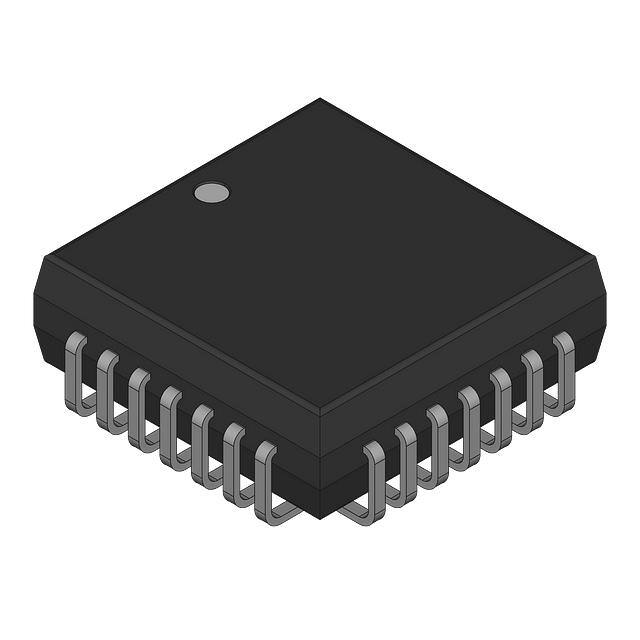


 工商网监
湘ICP备2023018690号
工商网监
湘ICP备2023018690号
