Test instrumentation
Microwave radios and very small aperture terminals (VSATs)
Military radios, radars, and electronic counter measures (ECMs)
Fiber optics and broadband telecommunications
GND 1
19 GND
21 GND
22 GND
20 RF2
18 GND
ADRF5040
GND 2
50Ω
50Ω
17 VDD
RFC 3
16 V1
GND 4
15 V2
GND 5
14 VSS
50Ω
50Ω
GND 6
PACKAGE
BASE
GND
14290-001
GND 12
RF3 11
9
GND
GND 10
8
RF4
13 GND
7
APPLICATIONS
23 RF1
FUNCTIONAL BLOCK DIAGRAM
Nonreflective 50 Ω design
Positive control range: 0 V to 3.3 V
Low insertion loss: 0.8 dB at 8.0 GHz
High isolation: 34 dB at 8.0 GHz
High power handling
33 dBm through path
27 dBm termination path
High linearity
1 dB compression (P1dB): 37 dBm typical
Input third-order intercept (IIP3): 58 dBm typical at 8.0 GHz
ESD rating: 4 kV human body model (HBM)
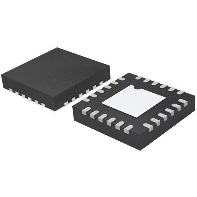
4 mm × 4 mm, 24-lead LFCSP package
No low frequency spurious
RF settling time (0.05 dB margin of final RFOUT): 9 µs
24 GND
FEATURES
GND
Data Sheet
High Isolation, Silicon SP4T,
Nonreflective Switch, 9 kHz to 12.0 GHz
ADRF5040
Figure 1.
GENERAL DESCRIPTION
The ADRF5040 is a general-purpose, broadband high isolation,
nonreflective single-pole, quad-throw (SP4T) switch in an LFCSP
surface-mount package. Covering the 9 kHz to 12.0 GHz range,
the switch offers high isolation and low insertion loss. The
switch features 34 dB isolation and 0.8 dB insertion loss up to
Rev. B
8.0 GHz, and a 9 µs settling time of 0.05 dB margin of the final
radio frequency output (RFOUT). The switch operates using
positive control voltage of 3.3 V and 0 V and requires +3.3 V and
−3.3 V supplies. The ADRF5040 is packaged in a 4 mm × 4 mm,
surface-mount LFCSP package.
Document Feedback
Information furnished by Analog Devices is believed to be accurate and reliable. However, no
responsibility is assumed by Analog Devices for its use, nor for any infringements of patents or other
rights of third parties that may result from its use. Specifications subject to change without notice. No
license is granted by implication or otherwise under any patent or patent rights of Analog Devices.
Trademarks and registered trademarks are the property of their respective owners.
One Technology Way, P.O. Box 9106, Norwood, MA 02062-9106, U.S.A.
Tel: 781.329.4700 ©2016–2017 Analog Devices, Inc. All rights reserved.
Technical Support
www.analog.com
�ADRF5040
Data Sheet
TABLE OF CONTENTS
Features .............................................................................................. 1
Interface Schematics .....................................................................7
Applications ....................................................................................... 1
Typical Performance Characteristics ..............................................8
Functional Block Diagram .............................................................. 1
Insertion Loss, Return Loss, and Isolation ................................8
General Description ......................................................................... 1
Input Power Compression and Input Third-Order Intercept ... 10
Revision History ............................................................................... 2
Specifications..................................................................................... 3
Input Power Compression and Input Third-Order Intercept,
10 kHz to 1 GHz .......................................................................... 11
Electrical Specifications ............................................................... 3
Theory of Operation ...................................................................... 12
Digital Control Voltage Specifications....................................... 4
Applications Information .............................................................. 13
Bias and Supply Current Specifications ..................................... 4
Evaluation Board ........................................................................ 13
Absolute Maximum Ratings ............................................................ 5
Outline Dimensions ....................................................................... 14
ESD Caution .................................................................................. 5
Ordering Guide .......................................................................... 14
Pin Configuration and Function Descriptions ............................. 6
REVISION HISTORY
7/2017—Rev. A to Rev. B
Changes to Figure 2, Figure 3, and Figure 4.................................. 5
2/2017—Rev. 0 to Rev. A
Changes to Ordering Guide .......................................................... 14
7/2016—Revision 0: Initial Version
Rev. B | Page 2 of 14
�Data Sheet
ADRF5040
SPECIFICATIONS
ELECTRICAL SPECIFICATIONS
VDD = 3.3 V, VSS = −3.3 V, V1 and V2 = 0 V or VDD, TA = 25°C, 50 Ω system, unless otherwise noted.
Table 1.
Parameter
INSERTION LOSS
Test Conditions/Comments
Min
Typ
Max
Unit
9 kHz to 4.0 GHz
9 kHz to 8.0 GHz
9 kHz to 10.0 GHz
9 kHz to 12.0 GHz
0.7
0.8
1.1
2
dB
dB
dB
dB
9 kHz to 4.0 GHz
9 kHz to 8.0 GHz
9 kHz to 10.0 GHz
9 kHz to 12.0 GHz
44
34
29.2
20
dB
dB
dB
dB
9 kHz to 4.0 GHz
9 kHz to 8.0 GHz
9 kHz to 10.0 GHz
9 kHz to 12.0 GHz
9 kHz to 4.0 GHz
9 kHz to 8.0 GHz
9 kHz to 10.0 GHz
9 kHz to 12.0 GHz
21
19
13.5
8
25
18.6
15.5
14.5
dB
dB
dB
dB
dB
dB
dB
dB
50% V1/V2 to 0.05 dB margin of final RFOUT
50% V1/V2 to 0.1 dB margin of final RFOUT
9
7
µs
µs
10% to 90% RFOUT
50% V1/V2 to 90%/10% RF
9 kHz to 12.0 GHz
1.3
3.5
µs
µs
37
34
dBm
dBm
62
58
53
dBm
dBm
dBm
ISOLATION, RFC TO RF1 TO RF4 (WORST CASE)
RETURN LOSS
On State
Off State
RADIO FREQUENCY (RF) SETTLING TIME
SWITCHING SPEED
tRISE/tFALL
tON/tOFF
INPUT POWER
1 dB Compression (P1dB)
0.1 dB Compression (P0.1dB)
INPUT THIRD-ORDER INTERCEPT (IIP3)
RECOMMENDED OPERATING CONDITIONS
Positive Supply Voltage (VDD)
Negative Supply Voltage (VSS)
Control Voltage (V1, V2) Range
RF Input Power
Through Path
Termination Path
Hot Switch Power Level
Case Temperature Range (TCASE)
Two-tone input power = 14 dBm at each tone
1 MHz to 2.0 GHz
1 MHz to 8.0 GHz
1 MHz to 12.0 GHz
3.0
−3.6
0
3.6
−3.0
VDD
V
V
V
−40
33
27
27
+85
dBm
dBm
dBm
°C
VDD = 3.3 V, VSS = −3.3 V, TA = 85°C, frequency = 2 GHz
VDD = 3.3 V, TA = 85°C, frequency = 2 GHz
Rev. B | Page 3 of 14
�ADRF5040
Data Sheet
DIGITAL CONTROL VOLTAGE SPECIFICATIONS
VDD = 3.3 V ± 10%, VSS = −3.3 V ± 10%, TCASE = −40°C to +85°C, unless otherwise noted.
Table 2.
Parameter
INPUT CONTROL VOLTAGE (V1, V2)
Low
High
Symbol
Min
VIL
VIH
0
1.4
Typ
Max
Unit
0.8
VDD + 0.3
V
V
Test Condition/Comments
很抱歉,暂时无法提供与“ADRF5040BCPZ-R7”相匹配的价格&库存,您可以联系我们找货
免费人工找货- 国内价格
- 1+134.61120
- 30+130.78800
- 国内价格
- 10+93.17000
- 50+91.47600
- 100+88.93500
- 500+87.24100
- 1000+86.39400
- 3000+84.70000


 工商网监
湘ICP备2023018690号
工商网监
湘ICP备2023018690号