GaAs, pHEMT, MMIC,
1 W Power Amplifier, 0.1 GHz to 6 GHz
HMC637ALP5E
Data Sheet
1
2
3
4
5
6
7
8
HMC637ALP5E
NIC 9
NIC 10
NIC 11
GND 12
VGG1 13
NIC 14
ACG4 15
ACG3 16
Telecom infrastructure
Microwave radio
Very small aperture terminal (VSAT)
Military and space
Test instrumentation
Fiber optics
NIC
VGG2
NIC
GND
RFIN
NIC
NIC
NIC
NIC = NO INTERNAL CONNECTION
24
23
22
21
20
19
18
17
NIC
NIC
GND
RFOUT/VDD
NIC
NIC
NIC
NIC
17308-001
APPLICATIONS
NIC
NIC
ACG1
ACG2
NIC
NIC
NIC
NIC
FUNCTIONAL BLOCK DIAGRAM
P1dB output power: 29 dBm
Gain: 13 dB
Output IP3: 44 dBm
50 Ω matched input/output
32-lead, 5 mm × 5 mm LFCSP package: 25 mm2
32
31
30
29
28
27
26
25
FEATURES
Figure 1.
GENERAL DESCRIPTION
The HMC637ALP5E is a gallium arsenide (GaAs), monolithic
microwave integrated circuit (MMIC), pseudomorphic high
electron mobility transistor (pHEMT) distributed power
amplifier which operates between 0.1 GHz and 6 GHz. The
amplifier provides 13 dB of gain, 44 dBm output third-order
intercept (IP3), and 29 dBm of output power at 1 dB gain
compression while requiring 400 mA from a 12 V supply. Gain
Rev. C
flatness is ±0.75 dB from 100 MHz to 6 GHz making the
HMC637ALP5E ideal for electronic warfare (EW), electronic
counter-measure (ECM), radar and test equipment applications.
The HMC637ALP5E amplifier radio frequency (RF) I/Os are
internally matched to 50 Ω, and the 5 mm × 5 mm lead frame
chip scale package (LFCSP) is compatible with high volume
surface-mount technology (SMT) assembly equipment.
Document Feedback
Information furnished by Analog Devices is believed to be accurate and reliable. However, no
responsibility is assumed by Analog Devices for its use, nor for any infringements of patents or other
rights of third parties that may result from its use. Specifications subject to change without notice. No
license is granted by implication or otherwise under any patent or patent rights of Analog Devices.
Trademarks and registered trademarks are the property of their respective owners.
One Technology Way, P.O. Box 9106, Norwood, MA 02062-9106, U.S.A.
Tel: 781.329.4700
©2019 Analog Devices, Inc. All rights reserved.
Technical Support
www.analog.com
�HMC637ALP5E
Data Sheet
TABLE OF CONTENTS
Features .............................................................................................. 1
ESD Caution...................................................................................4
Applications ....................................................................................... 1
Pin Configuration and Function Descriptions..............................5
Functional Block Diagram .............................................................. 1
Interface Schematics .....................................................................6
General Description ......................................................................... 1
Typical Performance Characteristics ..............................................7
Revision History ............................................................................... 2
Applications Information .................................................................9
Specifications..................................................................................... 3
Evaluation PCB ............................................................................... 10
Electrical Specifications ............................................................... 3
List of Materials for PCB EV1HMC637ALP5E ..................... 10
Absolute Maximum Ratings............................................................ 4
Outline Dimensions ....................................................................... 11
Thermal Resistance ...................................................................... 4
Ordering Guide .......................................................................... 11
REVISION HISTORY
This Hittite Microwave Products data sheet has been reformatted
to meet the styles and standards of Analog Devices, Inc.
4/2019—v02.0418 to Rev. C
Updated Format .................................................................. Universal
Changed HMC637ALP5 to HMC637ALP5E ........... Throughout
Changes to Product Title, Features Section, Applications
Section, General Description Section, and Figure 1 .................... 1
Changes to Electrical Specifications Section and Table 1 ........... 3
Changes to Table 2 ............................................................................ 4
Added Thermal Resistance Section ............................................... 4
Added Table 3; Renumbered Sequentially .....................................4
Added Figure 2; Renumbered Sequentially ...................................5
Changes to Table 4.............................................................................5
Changes to Figure 10 Caption through Figure 14 Caption .........7
Changes to Figure 15 Caption, Figure 16 Caption, Figure 18
Caption, and Figure 20 Caption ......................................................8
Changes to Application Information Section and Figure 21 .......9
Changes to List of Materials for PCB EV1HMC637ALP5E
Section and Table 5......................................................................... 10
Changes to Ordering Guide .......................................................... 11
Rev. C | Page 2 of 11
�Data Sheet
HMC637ALP5E
SPECIFICATIONS
ELECTRICAL SPECIFICATIONS
TA = 25°C, drain bias voltage (VDD) = 12 V, gate bias voltage (VGG2) = 5 V, supply current (IDD) = 400 mA (adjust VGG1 between −2 V to 0 V to
achieve IDD = 400 mA typical), 50 Ω system, unless otherwise noted.
Table 1.
Parameter
FREQUENCY RANGE
GAIN
Gain Flatness
Gain Variation Over Temperature
RETURN LOSS
Input
Output
OUTPUT
Output Power for 1 dB Compression
Saturated Output Power
Output Third-Order Intercept
NOISE FIGURE
Symbol
P1dB
PSAT
OIP3
Test Conditions/Comments
Min
0.1
12
27
POUT per tone = 10 dBm, 1 MHz spacing
2.0 GHz to 6.0 GHz
SUPPLY CURRENT
Drain Bias Voltage1
1
IDD
VDD
320
IDD = 400 mA
Typ
Max
6
13
±0.75
0.015
Units
GHz
dB
dB
dB/°C
12
15
dB
dB
29
31
44
12
5
400
11.5
12.0
12.5
dBm
dBm
dBm
dB
dB
mA
V
V
V
480
VGG1 set initially for nominal bias condition of VDD = 12 V and VGG2 = 5 V to achieve IDD = 400 mA typical; then adjusting VDD ±0.5 V from 12 V to measure IDD variation.
Rev. C | Page 3 of 11
�HMC637ALP5E
Data Sheet
ABSOLUTE MAXIMUM RATINGS
THERMAL RESISTANCE
Table 2.
Parameter
Drain Bias Voltage (VDD)
Gate Bias Voltage
VGG1
VGG2
RF Input Power (RFIN), VDD = 12 VDC
Channel Temperature
Continuous PDISS (T = 85°C, Derate
95 mW/°C Above 85°C)
Maximum Peak Reflow Temperature
Storage Temperature Range
Operating Temperature Range
Electrostatic Discharge (ESD) Sensitivity
Human Body Model (HBM)
1
Rating
14 VDC
Thermal performance is directly linked to printed circuit
board (PCB) design and operating environment. Careful
attention to PCB thermal design is required.
−3 VDC to 0 VDC
4 VDC to 7 VDC
25 dBm
175°C
8.6 W
θJC is the junction to case thermal resistance.
Table 3. Thermal Resistance
Package Type
HCP-32-1
260°C (MSL31 Rating)
−65°C to +150°C
−40°C to +85°C
1
θJC1
10.5
Unit
°C/W
Thermal impedance simulated values are based on a JEDEC 1S0P thermal
test board. See JEDEC JESD51.
ESD CAUTION
Class 1B
MSL3 stands for Moisture Sensitivity Level 3.
Stresses at or above those listed under Absolute Maximum
Ratings may cause permanent damage to the product. This is a
stress rating only; functional operation of the product at these
or any other conditions above those indicated in the operational
section of this specification is not implied. Operation beyond
the maximum operating conditions for extended periods may
affect product reliability.
Rev. C | Page 4 of 11
�Data Sheet
HMC637ALP5E
32
31
30
29
28
27
26
25
NIC
NIC
ACG1
ACG2
NIC
NIC
NIC
NIC
PIN CONFIGURATION AND FUNCTION DESCRIPTIONS
1
2
3
4
5
6
7
8
HMC637ALP5E
TOP VIEW
(Not to Scale)
24
23
22
21
20
19
18
17
NIC
NIC
GND
RFOUT/VDD
NIC
NIC
NIC
NIC
NOTES
1. NIC = NO INTERNAL CONNECTION. THESE PINS MAY BE CONNECTED TO
RF GROUND. PERFORMANCE IS NOT AFFECTED.
2. EXPOSED PAD. THE EXPOSED PAD MUST BE CONNECTED TO RF/DC GROUND.
17308-002
NIC 9
NIC 10
NIC 11
GND 12
VGG1 13
NIC 14
ACG4 15
ACG3 16
NIC
VGG2
NIC
GND
RFIN
NIC
NIC
NIC
Figure 2. Pin Configuration
Table 4. Pin Function Descriptions
Pin No.
1, 3, 6 to 11, 14, 17 to 20, 23 to 28, 31, 32
Mnemonic
NIC
2
VGG2
4, 12, 22
5
13
GND
RFIN
VGG1
15
ACG4
16
ACG3
21
RFOUT/VDD
29
ACG2
30
ACG1
EPAD
1
Description1
No Internal Connection. These pins may be connected to RF ground. Performance
is not affected.
Gate Control 2 for Amplifier. Apply 5 V to VGG2 for nominal operation. Attach a bypass
capacitor per the application circuit shown in the Applications Information section.
Ground. Connect Pin 4, Pin 12, and Pin 22 to RF/dc ground.
This pad is dc-coupled and matched to 50 Ω.
Gate Control 1 for Amplifier. Attach a bypass capacitor per the application circuit
shown in the Applications Information section. Follow the power up and power
down sequences outlines in the Applications Information section.
Low Frequency Termination. Attach a bypass capacitor per the application circuit
shown in the Applications Information section.
Low Frequency Termination. Attach a bypass capacitor per the application circuit
shown in the Applications Information section.
RF Output/Power Supply Voltage for Amplifier. Connect the dc bias (VDD) network
to provide drain current (IDD). See the application circuit shown in the
Applications Information section.
Low Frequency Termination. Attach a bypass capacitor per the application circuit
shown in the Applications Information section.
Low Frequency Termination. Attach a bypass capacitor per the application circuit
shown in the Applications Information section.
Exposed Pad. The exposed pad must be connected to RF/dc ground.
See the Interface Schematics section for pin interfaces.
Rev. C | Page 5 of 11
�HMC637ALP5E
Data Sheet
INTERFACE SCHEMATICS
ACG4
17308-003
VGG2
RFIN
17308-006
ACG3
Figure 6. RFIN, ACG4, and ACG3 Interface Schematic
Figure 3. VGG2 Interface Schematic
ACG1
RFOUT/VDD
17308-007
17308-004
ACG2
VGG1
Figure 7. VGG1 Interface Schematic
Figure 4. ACG1, ACG2, and RFOUT/VDD Interface Schematic
GND
17308-008
17308-005
RFIN
Figure 5. RFIN Interface Schematic
Figure 8. GND Interface Schematic
Rev. C | Page 6 of 11
�Data Sheet
HMC637ALP5E
TYPICAL PERFORMANCE CHARACTERISTICS
20
18
16
14
12
0
GAIN (dB)
S21
S11
S22
–10
+85°C
+25°C
–40°C
10
8
6
4
–20
17308-009
2
–30
0
2
4
6
17308-012
RESPONSE (dB)
10
0
8
0
2
FREQUENCY (GHz)
Figure 9. Gain and Return Loss
6
8
Figure 12. Gain vs. Frequency at Various Temperatures
0
0
–5
–5
+85°C
+25°C
–40°C
–10
RETURN LOSS (dB)
–15
–20
–25
+85°C
+25°C
–40°C
–10
–15
–20
17308-010
–25
–30
0
2
4
6
17308-013
RETURN LOSS (dB)
4
FREQUENCY (GHz)
–30
8
0
2
FREQUENCY (GHz)
4
6
8
FREQUENCY (GHz)
Figure 10. Input Return Loss vs. Frequency at Various Temperatures
Figure 13. Output Return Loss vs. Frequency at Various Temperatures
24
0
22
20
+85°C
+25°C
–40°C
–20
18
NOISE FIGURE (dB)
ISOLATION (dB)
–10
–30
–40
16
+85°C
+25°C
–40°C
14
12
10
8
17308-011
–60
0
2
4
6
17308-014
6
–50
4
2
0
8
FREQUENCY (GHz)
2
4
6
8
FREQUENCY (GHz)
Figure 11. Reverse Isolation vs. Frequency at Various Temperatures
Figure 14. Noise Figure vs. Frequency at Various Temperatures
Rev. C | Page 7 of 11
�HMC637ALP5E
32
32
30
30
28
PSAT (dB)
+85°C
+25°C
–40°C
26
26
24
22
22
17308-015
24
20
0
2
+85°C
+25°C
–40°C
4
6
17308-018
28
P1dB (dBm)
Data Sheet
20
8
0
2
FREQUENCY (GHz)
Figure 15. P1dB vs. Frequency at Various Temperatures
6
8
Figure 18. PSAT vs. Frequency at Various Temperatures
50
55
+85°C
+25°C
–40°C
50
45
40
35
30
17308-016
25
20
0
2
4
6
45
OIP3
PSAT
P1DB
GAIN
40
35
30
25
30
15
17308-019
GAIN (dB), P1dB (dBm), PSAT (dBm), IP3 (dBm)
60
OUTPUT IP3 (dBm)
4
FREQUENCY (GHz)
10
11.5
8
12.0
12.5
VDD (V)
FREQUENCY (GHz)
Figure 16. Output IP3 vs. Frequency at Various Temperatures
Figure 19. Gain, Power, and Output IP3 vs. Supply Voltage at 3 GHz, Fixed VGG
20
60
55
10
OUTPUT IP3 (dBm)
S21
S11
S22
0
–10
+85°C
+25°C
–40°C
45
40
35
30
–20
0.1
1
20
0.01
10
FREQUENCY (GHz)
Figure 17. Gain and Return Loss vs. Frequency, Log Scale
17308-020
–30
0.01
25
17308-017
RESPONSE (dB)
50
0.1
1
10
FREQUENCY (GHz)
Figure 20. Output IP3 vs. Frequency at Various Temperatures, Log Scale
Rev. C | Page 8 of 11
�Data Sheet
HMC637ALP5E
APPLICATIONS INFORMATION
The power-down sequence is as follows:
For the application circuit shown in Figure 21, VDD must be
applied through a broadband bias tee or external bias network.
1.
2.
3.
The power-up bias sequence is as follows:
Set VGG1 to −2 V
Set VDD to 12 V
Set VGG2 to 5 V
Adjust VGG1 to achieve IDD for 400 mA
C4
1000pF
C7
4.7µF
+
ACG1
ACG2
VDD
30
VGG2
2
C3
1000pF
29
C1
1000pF
HMC637ALP5E
21
RFOUT
16
5
RFIN
ACG3
15
ACG4
13
VGG1
C9
4.7µF +
C2
100pF
C8
+ 4.7µF
C6
1000pF
C5
1000pF
Figure 21. Application Circuit
Rev. C | Page 9 of 11
17308-021
1.
2.
3.
4.
Remove VGG2 bias
Remove VDD bias
Remove VGG1 bias
�HMC637ALP5E
Data Sheet
17308-022
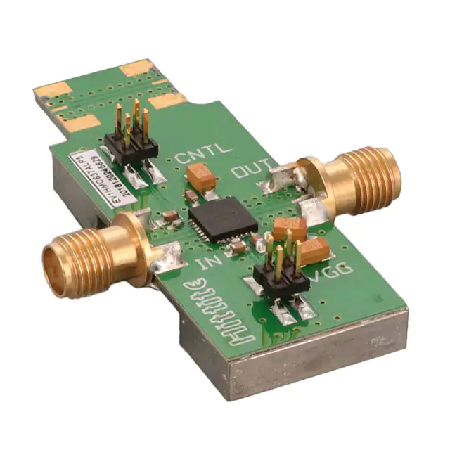
EVALUATION PCB
Figure 22. Evaluation Board PCB
LIST OF MATERIALS FOR PCB EV1HMC637ALP5E
It is recommended that the circuit board used in the application
follows proper RF circuit design techniques. Signal lines must
have 50 Ω impedance while the package ground leads and
package bottom are connected directly to the ground plane
similar to that shown in Figure 22. Ensure that a sufficient
number of via holes are used to connect the top and bottom
ground planes. The evaluation board thermal design must also
be considered and mounted to an appropriate heat sink. The
evaluation circuit board shown is available from Analog
Devices, Inc. upon request.
Table 5. Bill of Materials for Evaluation PCB
EV1HMC637ALP5E
Item
J1, J2
J3, J4
C1, C2
C3 to C6
C7 to C9
U1
PCB1
1
Description
SRI SMA connector
2 mm Molex header
100 pF capacitor, 0402 package
1000 pF capacitor, 0603 package
4.7 μF capacitor, tantalum
HMC637ALP5E
109765 evaluation PCB
Circuit board material: Rogers 4350.
Rev. C | Page 10 of 11
�Data Sheet
HMC637ALP5E
OUTLINE DIMENSIONS
DETAIL A
(JEDEC 95)
5.10
5.00 SQ
4.90
0.30
0.25
0.18
1
24
0.50
BSC
3.80
3.70 SQ
3.60
EXPOSED
PAD
17
0.45
0.40
0.35
TOP VIEW
0.90
0.85
0.80
PKG-004898
8
16
0.05 MAX
0.02 NOM
COPLANARITY
0.08
0.20 REF
SEATING
PLANE
P IN 1
IN D IC ATO R AR E A OP T IO N S
(SEE DETAIL A)
32
25
9
BOTTOM VIEW
3.50 REF
0.20 MIN
FOR PROPER CONNECTION OF
THE EXPOSED PAD, REFER TO
THE PIN CONFIGURATION AND
FUNCTION DESCRIPTIONS
SECTION OF THIS DATA SHEET.
COMPLIANT TO JEDEC STANDARDS MO-220-VHHD-4
02-19-2019-B
PIN 1
INDICATOR
AREA
Figure 23. 32-Lead Lead Frame Chip Scale Package [LFCSP]
5 mm × 5 mm and 0.85 mm Package Height
(HCP-32-1)
Dimensions shown in millimeters
ORDERING GUIDE
Model1
HMC637ALP5E
HMC637ALP5ETR
EV1HMC637ALP5
1
2
Temperature Range
−40°C to +85°C
−40°C to +85°C
MSL Rating2
MSL3
MSL3
Package Description
32-Lead Lead Frame Chip Scale Package [LFCSP]
32-Lead Lead Frame Chip Scale Package [LFCSP]
Evaluation Board
All devices are RoHS compliant.
See the Absolute Maximum Ratings section.
©2019 Analog Devices, Inc. All rights reserved. Trademarks and
registered trademarks are the property of their respective owners.
D17308-0-4/19(C)
Rev. C | Page 11 of 11
Package Option
HCP-32-1
HCP-32-1
�


 工商网监
湘ICP备2023018690号
工商网监
湘ICP备2023018690号
