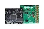
EVAL-AD5676SDZ/
EVAL-AD5676RSDZ User Guide
UG-814
One Technology Way • P.O. Box 9106 • Norwood, MA 02062-9106, U.S.A. • Tel: 781.329.4700 • Fax: 781.461.3113 • www.analog.com
Evaluating the AD5676/AD5676R Octal, 16-Bit nanoDAC+
FEATURES
GENERAL DESCRIPTION
Full featured evaluation board for the AD5676/AD5676R
Various link options
PC control in conjunction with the Analog Devices, Inc.,
EVAL-SDP-CB1Z system demonstration platform (SDP)
This user guide details the operation of the evaluation boards
for the AD5676/AD5676R octal channel, voltage output digitalto-analog converter (DAC).
EVALUATION KIT CONTENTS
EVAL-AD5676SDZ/EVAL-AD5676RSDZ evaluation board
ADDITIONAL EQUIPMENT AND SOFTWARE NEEDED
EVAL-SDP-CB1Z SDP board, includes a USB cable
Bench power supply (6 V dc)
PC running Windows 7 or later with USB 2.0 port
ONLINE RESOURCES
Documents Needed
AD5676/AD5676R data sheet
EVAL-AD5676SDZ/EVAL-AD5676RSDZ user guide
Required Software
ACE software
The EVAL-AD5676SDZ/EVAL-AD5676RSDZ evaluation
boards help users to quickly prototype new AD5676/AD5676R
circuits and reduce design time. The AD5676/AD5676R operate
from a single 2.7 V to 5.5 V supply. The AD5676R has an internal
2.5 V reference giving a maximum output voltage of 2.5 V or 5 V.
The AD5676 does not have an internal reference; therefore, an
ADR431 is provided on-board as a 2.5 V reference source. A
different reference voltage can be applied via the EXT_REF SMB
connector, if required.
Full data on the AD5676/AD5676R are available in the respective
product data sheets, available from Analog Devices, which should
be consulted in conjunction with this user guide when using the
evaluation boards.
The evaluation boards interface to the USB port of a PC via the
SDP board. The Analysis Control Evaluation (ACE) software is
available for use with the evaluation board to allow the user to
program the AD5676/AD5676R.
The evaluation boards are compatible with the EVAL-SDP-CB1Z
Blackfin® SDP controller board (SDP-B), which is available for
order on the Analog Devices website at www.analog.com.
PLEASE SEE THE LAST PAGE FOR AN IMPORTANT
WARNING AND LEGAL TERMS AND CONDITIONS.
Rev. A | Page 1 of 12
�UG-814
EVAL-AD5676SDZ/EVAL-AD5676RSDZ User Guide
TABLE OF CONTENTS
Features .............................................................................................. 1
Memory Map .................................................................................6
Evaluation Kit Contents ................................................................... 1
Evaluation Board Hardware .............................................................7
Additional Equipment and Software Needed................................... 1
Power Supplies ...............................................................................7
Online Resources .............................................................................. 1
Input Signals...................................................................................7
General Description ......................................................................... 1
Output Signals ...............................................................................7
Revision History ............................................................................... 2
Link Configuration Options ............................................................8
Typical Evaluation Setup ................................................................. 3
Setup Conditions ...........................................................................8
Getting Started .................................................................................. 4
Evaluation Board Circuitry ..............................................................9
Installing the Software ................................................................. 4
Evaluation Board Schematics........................................................ 10
Initial Setup ................................................................................... 4
Bill of Materials ............................................................................... 12
Block Diagram And Description .................................................... 5
REVISION HISTORY
5/2017—Rev. 0 to Rev. A
Changes to Features Section, Additional Equipment and
Software Needed Section, Online Resources Section, and
General Description Section ........................................................... 1
Changes to Installing the Software Section, Changed Evaluation
Board Setup Procedures Section to Initial Set-Up Section ......... 4
Added Figure 3 and Figure 4; Renumbered Sequentially ........... 4
Added Block Diagram and Description Section and Figure 4 ........ 5
Added Table 1; Renumbered Sequentially .................................... 5
Added Memory Map Section, Figure 5, and Figure 6 ................. 6
Deleted How to Use the Software Section ..................................... 8
Changes to Table 4 .......................................................................... 12
3/2015—Revision 0: Initial Version
Rev. A | Page 2 of 12
�EVAL-AD5676SDZ/EVAL-AD5676RSDZ User Guide
UG-814
TYPICAL EVALUATION SETUP
SDP BOARD
AD5676R EVALUATION BOARD
0.250A
6V
±25V
COM
POWER SUPPLY CONNECTORS
12993-001
6.000V
Figure 1.
Rev. A | Page 3 of 12
�UG-814
EVAL-AD5676SDZ/EVAL-AD5676RSDZ User Guide
GETTING STARTED
INSTALLING THE SOFTWARE
The EVAL-AD5676SDZ and EVAL-AD5676RSDZ evaluation
boards use the Analog Devices ACE software. ACE is a desktop
software application that allows the evaluation and control of
multiple evaluation systems.
The ACE installer installs necessary SDP drivers and .NET
Framework 4 by default. Install ACE before connecting the SDP
board to the USB port of the PC to ensure that the SDP board is
recognized when it connects to the PC. Use the following link
to download the software, and access full instructions on how
to install and use this software: http://www.analog.com/ace.
After the installation is finished, the EVAL-AD5676SDZ and
EVAL-AD5676RSDZ evaluation board plug-ins appear when
you open ACE.
Figure 2. Board View of the EVAL-AD5676RSDZ
INITIAL SETUP
1.
2.
3.
4.
5.
Connect the evaluation board to the SDP-B board and
connect the USB cable between the SDP-B board and the PC.
Power the SDP-B and evaluation board by connecting
6 V dc to the J3 connector.
Run the ACE application. The EVAL-AD5676SDZ/
EVAL-AD5676RSDZ board plug-ins appear in the
attached hardware section of the Start tab.
Double-click on the board plug-in to open the board view
seen in Figure 2.
The chip block diagram can be accessed by double-clicking
on the AD5676 or AD5676R chip. This view provides a
basic representation of functionality of the board. The
main functions are labeled in Figure 3.
Rev. A | Page 4 of 12
12993-003
To set up the evaluation board, take the following steps:
Figure 3. Chip Block Diagram View for the AD5676R
�EVAL-AD5676SDZ/EVAL-AD5676RSDZ User Guide
UG-814
BLOCK DIAGRAM AND DESCRIPTION
Some of the blocks and their functions are described here as
they pertain to the evaluation board. The full screen block
diagram is shown in Figure 4 and Table 1 describe the
functionality of each block.
12993-004
The EVAL-AD5676SDZ/EVAL-AD5676RSDZ software is
organized so that it appears similar to the functional block
diagram shown in the data sheets. In this way, it is easy to
correlate the functions on the board with the description in the
data sheets. A full description of each block, register, and its
settings is given in the AD5676/AD5676R data sheets.
Figure 4. Block Diagram with Labels
Table 1. Block Diagram Functions
Label
A
B
C
D
E
F
G
H
I
J
K
Function
The configuration wizard sets up the initial configuration for the board. From the Output Gain drop-down menu, the reference
gain case be selected. A gain of 1 is the default. After setting up the initial configuration, click Apply and the values are applied.
These settings can be modified at any stage while testing.
The GPIO buttons act as external GPIO pulses to the LDAC and RESET pins. The LDAC button pushes data from both input
registers (E) to the DAC registers (F). The RESET button clears all data from input registers and DAC registers. These buttons are
live, so there is no need to click Apply Changes (K).
The Command Option drop-down menu selects how the data being transferred to the device affects the Input and DAC registers.
After a data value is entered in an input register (see E), this menu determines if the data is transferred to the input register only, or
to the channel input register (E) and channel DAC register (F).
The Change Page Display drop-down menu selects which page of 4 DAC channel settings are displayed
The input registers transfer 16-bit data word to the device. Upon clicking the Apply Changes (K), this 16-bit data word is
transferred to the device.
The DAC registers display the value that is currently present in the DAC register on the device. The DAC registers can be updated
by selecting the appropriate command option or by toggling LDAC (B).
Software reset returns the board and software to default values. This button is live, so there is no need to click Apply Changes.
The Load LDAC buttons per channel control to control the loading of Input Register contents to the DAC Register.
The DAC Configuration options provide access to per channel configuration options such as power-down options and hardware
LDAC mask setting.
Selecting enabled from the internal reference setting enables the on-chip reference for the board, if disabled is selected, an
external reference must be applied. This control is only available on the AD5676R.
The Apply Changes button applies all modified values to the device. Note that if an evaluation board is not connected, values
entered into the Input Registers are not transferred to the DAC registers.
Rev. A | Page 5 of 12
�UG-814
EVAL-AD5676SDZ/EVAL-AD5676RSDZ User Guide
MEMORY MAP
12993-005
All registers are fully accessible from the memory map tab; this
allows registers to be edited at a bit level. The bits shaded in
dark gray are read only bits and cannot be accessed from ACE;
all other bits are toggled. Apply Changes is used to transfer data
to the device. All changes here correspond to the block diagram;
for example, if the internal register bit is enabled, it shows as
enabled on the block diagram. Any bits or registers that are in
bold are modified values that have not been transferred to the
board. After Apply Changes is clicked, the data is transferred to
the board.
12993-106
Figure 5. AD5676R Memory Map
Figure 6. AD5676R Memory Map with Unapplied Changes in DAC Input 0 Register
Rev. A | Page 6 of 12
�Evaluation Board User Guide
UG-815
EVALUATION BOARD HARDWARE
POWER SUPPLIES
INPUT SIGNALS
To use the evaluation board with the SDP-B board, a 6 V dc
power supply is required, which is connected to Connector J3.
The evaluation board can be used without the SDP-B board,
in which case, the J1 and J2 connectors are used as the power
supply inputs.
When the SDP-B board is used to control the evaluation board,
the digital input signals are applied to Connector J4. When the
SDP-B board is not used, apply the digital signal to Connector J5.
All supplies are decoupled to ground with 10 μF tantalum and
0.1 μF ceramic capacitors.
Voltage
External, VLOGIC supply
Analog power supply, VCC
6 V dc board positive power supply
EXT_REF
AGND
EXT_VDD
DGND
VREF
I2C
INTERFACE
10-WAY
HEADER
VOUT0
VOUT1
AD5675/
AD5675R
VOUT6
VOUT7
Figure 7. Evaluation Board Block Diagram
Rev. A | Page 7 of 13
12995-002
Connector Number
J1
J2
J3
ADR431
2.5V REF
EEPROM
SDP CONNECTOR
Table 2. Power Supply Connectors
EXT_VL
The DAC output voltages are available on the SMB connectors,
VOUT0 to VOUT7.
+6V
AGND
Both AGND and DGND inputs are provided on the board. The
AGND and DGND planes are connected at one location close
to the AD5676/AD5676R. It is recommended that AGND and
DGND not be connected elsewhere in the system to avoid
ground loop problems.
OUTPUT SIGNALS
�UG-814
EVAL-AD5676SDZ/EVAL-AD5676RSDZ User Guide
LINK CONFIGURATION OPTIONS
Multiple link (LKx) options must be set correctly to select the
appropriate operating setup before using the evaluation board.
The functions of these options are described in Table 3.
board. The evaluation boards can be operated in SDP controlled
mode to be used with the SDP-B board, or the evaluation board
can be used in standalone mode.
SETUP CONDITIONS
The Default Position column of Table 3 shows the default
positions in which the links are set when the evaluation board
is packaged. When the board is shipped, it is set up to operate
with the SDP-B board in SDP controlled mode.
Before applying power and signals to the evaluation board,
ensure that all link positions are as required by the operating
mode. There are two modes in which to operate the evaluation
Table 3. Link Functions
Link No.
LK1
LK2
LK3
LK4
LK5
1
Function
This link selects the DAC analog voltage source.
Position A selects the internal voltage source (INT_VCC) from the ADP3331 (U1).
Position B selects an external supply voltage (EXT_ VCC).
This link selects the DAC digital voltage source.
Position A selects the digital voltage source from the SDP-B board (V_IO).
Position B selects an external digital supply voltage (EXT_VLOGIC).
This link selects the reference source.
Position A selects the internal reference of the AD5676R as the reference source or an external reference source
from the SMB connector EXT_REF. Use only Position A with the EVAL-AD5676RSDZ.
Position B selects U6 as the 2.5 V reference source. Do not use Position B with the EVAL-AD5676RSDZ.
This link selects the RSTSEL setting of the AD5676/AD5676R.
Position A selects DAC power up to zero scale.
Position B selects DAC power up to midscale.
This link sets the internal gain setting of the AD5676/AD5676R.
Position A selects software control of the gain via the SDP-B board.
Position B selects a gain of 0 V to 2 × VREF.
Position C selects a gain of 0 V to VREF.
Position A is the default for the EVAL-AD5676RSDZ. Position B is the default for the EVAL-AD5676SDZ.
Rev. A | Page 8 of 12
Default
Position
A
A
A/B 1
A
A
�EVAL-AD5676SDZ/EVAL-AD5676RSDZ User Guide
UG-814
EVALUATION BOARD CIRCUITRY
The EVAL-AD5676SDZ/EVAL-AD5676RSDZ evaluation
boards allow the function and performance of the AD5676/
AD5676R to be easily tested. Each evaluation board contains two
voltage regulators that generate the analog and digital power
supplies and that also power the SDP-B board, if it is connected.
The two regulators are powered via a 6 V supply attached to
Connector J3. Alternatively, a separate analog supply can be
attached via Connector J2, and an external VLOGIC supply can be
connected to Connector J1.
Control of the AD5676/AD5676R is typically performed by the
SDP-B board, which is attached to Connector J4. The SDP-B
board allows the software provided with the kit to be used to
load register values, set the voltage of the DAC outputs, and
write to the control register of the AD5676/AD5676R. When
the SDP-B board is not required, the control signals can be
applied to the AD5676/AD5676R by connecting them to the
relevant pins on Connector J5.
The DAC output voltages are available on the SMB connectors,
VOUT0 to VOUT7.
Rev. A | Page 9 of 12
�UG-814
EVAL-AD5676SDZ/EVAL-AD5676RSDZ User Guide
EVALUATION BOARD SCHEMATICS
12993-006
Figure 8. EVAL-AD5676SDZ/EVAL-AD5676RSDZ Schematic, Page 1 of 2
Rev. A | Page 10 of 12
�EVAL-AD5676SDZ/EVAL-AD5676RSDZ User Guide
UG-814
12993-007
Figure 9. EVAL-AD5676SDZ/EVAL-AD5676RSDZ Schematic, Page 2 of 2
Rev. A | Page 11 of 12
�UG-814
EVAL-AD5676SDZ/EVAL-AD5676RSDZ User Guide
BILL OF MATERIALS
Table 4.
Qty
7
7
1
17
Description
Capacitor, Case A, 10 µF, 10 V
Capacitor, 100 nF, 50 V, 0603
Capacitor, 1 µF, 10 V, 0603
Do not populate
Supplier/Part Number 1
FEC 197-130
FEC 8820023
FEC 318-8840
Not inserted
3
1
1
1
3
1
1
1
1
1
1
4
2
9
1
1
1
1
1
Reference Designator
C1, C3, C5, C7 to C9, C16
C2, C4, C6, C10 to C12, C15
C14
C13, C17 to C19, C24 to C27,
R5 to R7, R10, R12 to R16
J1 to J3
J4
J5
L1
LK1 to LK3
LK4
LK5
R1
R2
R3
R4
R8, R9, R19, R20
R17, R18
TP1 to TP9
U1
U2
U3
U6
U8
2-pin terminal block
120-way female connector
10-pin (2 × 5), 0.1" header
Ferrite bead, 600 Ω at 100 MHz
Jumper block using 3-pin SIP header
2-way link option
3-way link option
Resistor, 1 MΩ, 0.063 W, 1%, 0603
Resistor, 300 kΩ, 0.1 W, 1%, 0603
Resistor, 1.5 Ω, 0.063 W, 5%, 0603
Resistor, 0 Ω, 0805
10 kΩ, SMD, resistor
100 kΩ, SMD, resistor
Red test point
Adjustable LDO regulator
32k I2C serial EEPROM
5 V, fixed, adjustable voltage regulator
Ultralow noise XFET voltage reference
Octal,16-bit nanoDAC+
9
VOUT0 to VOUT7, EXT_REF
Straight PCB mount SMB jack, 50 Ω
FEC 151789
FEC 1324660 or Digikey H1219-ND
FEC 1022244 (36-pin strip)
Digikey 490-1024-1-ND
FEC 1022248 and 150410
FEC 1022244
FEC 9331662
Digikey RMCF1/161MFRCT-ND
Digikey 541-300KHCT-ND
FEC 9331832
FEC 9333681
FEC 933-0399
FEC 9330402
FEC 8731144 (pack)
Analog Devices ADP3331ARTZ
FEC 1331330
Analog Devices ADP3367ARZ
Analog Devices ADR431BRZ
Analog Devices AD5676RARUZ
or AD5676ARUZ
FEC 1206013
1
FEC is Farnell Electronics Components.
ESD Caution
ESD (electrostatic discharge) sensitive device. Charged devices and circuit boards can discharge without detection. Although this product features patented or proprietary protection
circuitry, damage may occur on devices subjected to high energy ESD. Therefore, proper ESD precautions should be taken to avoid performance degradation or loss of functionality.
Legal Terms and Conditions
By using the evaluation board discussed herein (together with any tools, components documentation or support materials, the “Evaluation Board”), you are agreeing to be bound by the terms and conditions
set forth below (“Agreement”) unless you have purchased the Evaluation Board, in which case the Analog Devices Standard Terms and Conditions of Sale shall govern. Do not use the Evaluation Board until you
have read and agreed to the Agreement. Your use of the Evaluation Board shall signify your acceptance of the Agreement. This Agreement is made by and between you (“Customer”) and Analog Devices, Inc.
(“ADI”), with its principal place of business at One Technology Way, Norwood, MA 02062, USA. Subject to the terms and conditions of the Agreement, ADI hereby grants to Customer a free, limited, personal,
temporary, non-exclusive, non-sublicensable, non-transferable license to use the Evaluation Board FOR EVALUATION PURPOSES ONLY. Customer understands and agrees that the Evaluation Board is provided
for the sole and exclusive purpose referenced above, and agrees not to use the Evaluation Board for any other purpose. Furthermore, the license granted is expressly made subject to the following additional
limitations: Customer shall not (i) rent, lease, display, sell, transfer, assign, sublicense, or distribute the Evaluation Board; and (ii) permit any Third Party to access the Evaluation Board. As used herein, the term
“Third Party” includes any entity other than ADI, Customer, their employees, affiliates and in-house consultants. The Evaluation Board is NOT sold to Customer; all rights not expressly granted herein, including
ownership of the Evaluation Board, are reserved by ADI. CONFIDENTIALITY. This Agreement and the Evaluation Board shall all be considered the confidential and proprietary information of ADI. Customer may
not disclose or transfer any portion of the Evaluation Board to any other party for any reason. Upon discontinuation of use of the Evaluation Board or termination of this Agreement, Customer agrees to
promptly return the Evaluation Board to ADI. ADDITIONAL RESTRICTIONS. Customer may not disassemble, decompile or reverse engineer chips on the Evaluation Board. Customer shall inform ADI of any
occurred damages or any modifications or alterations it makes to the Evaluation Board, including but not limited to soldering or any other activity that affects the material content of the Evaluation Board.
Modifications to the Evaluation Board must comply with applicable law, including but not limited to the RoHS Directive. TERMINATION. ADI may terminate this Agreement at any time upon giving written notice
to Customer. Customer agrees to return to ADI the Evaluation Board at that time. LIMITATION OF LIABILITY. THE EVALUATION BOARD PROVIDED HEREUNDER IS PROVIDED “AS IS” AND ADI MAKES NO
WARRANTIES OR REPRESENTATIONS OF ANY KIND WITH RESPECT TO IT. ADI SPECIFICALLY DISCLAIMS ANY REPRESENTATIONS, ENDORSEMENTS, GUARANTEES, OR WARRANTIES, EXPRESS OR IMPLIED, RELATED
TO THE EVALUATION BOARD INCLUDING, BUT NOT LIMITED TO, THE IMPLIED WARRANTY OF MERCHANTABILITY, TITLE, FITNESS FOR A PARTICULAR PURPOSE OR NONINFRINGEMENT OF INTELLECTUAL
PROPERTY RIGHTS. IN NO EVENT WILL ADI AND ITS LICENSORS BE LIABLE FOR ANY INCIDENTAL, SPECIAL, INDIRECT, OR CONSEQUENTIAL DAMAGES RESULTING FROM CUSTOMER’S POSSESSION OR USE OF
THE EVALUATION BOARD, INCLUDING BUT NOT LIMITED TO LOST PROFITS, DELAY COSTS, LABOR COSTS OR LOSS OF GOODWILL. ADI’S TOTAL LIABILITY FROM ANY AND ALL CAUSES SHALL BE LIMITED TO THE
AMOUNT OF ONE HUNDRED US DOLLARS ($100.00). EXPORT. Customer agrees that it will not directly or indirectly export the Evaluation Board to another country, and that it will comply with all applicable
United States federal laws and regulations relating to exports. GOVERNING LAW. This Agreement shall be governed by and construed in accordance with the substantive laws of the Commonwealth of
Massachusetts (excluding conflict of law rules). Any legal action regarding this Agreement will be heard in the state or federal courts having jurisdiction in Suffolk County, Massachusetts, and Customer hereby
submits to the personal jurisdiction and venue of such courts. The United Nations Convention on Contracts for the International Sale of Goods shall not apply to this Agreement and is expressly disclaimed.
©2015–2017 Analog Devices, Inc. All rights reserved. Trademarks and
registered trademarks are the property of their respective owners.
UG12993-0-5/17(A)
Rev. A | Page 12 of 12
�


 工商网监
湘ICP备2023018690号
工商网监
湘ICP备2023018690号

