EVAL-ADM2795EEBZ User Guide
UG-997
One Technology Way • P.O. Box 9106 • Norwood, MA 02062-9106, U.S.A. • Tel: 781.329.4700 • Fax: 781.461.3113 • www.analog.com
Certified Evaluation Board for the ADM2795E Robust 5 kV rms Isolated RS-485/RS-422
Transceiver with Level 4 EMC and Full ±42 V Protection
FEATURES
GENERAL DESCRIPTION
5 kV rms signal isolated RS-485/RS-422 transceiver
Convenient connections for power supplies and signals
through screw terminal blocks and jumper connections
1.7 V to 5.5 V operating voltage range on VDD1 logic supply
3 V to 5.5 V operating voltage range on VDD2
Certified RS-485 A, B bus pin protection, passing
IEC 61000-4-5 surge to ±4 kV
IEC 61000-4-4 electrical fast transient (EFT) to ±2 kV
IEC 61000-4-2 electrostatic discharge (ESD) to
±8 kV (contact)
±15 kV (air)
IEC 61000-4-6 conducted radio frequency (RF) immunity to
Level 3 (10 V/m rms)
Human body model (HBM) ESD to > ±30 kV
Certified IEC electromagnetic compatibility (EMC) immunity
provided by isolation barrier, withstands
IEC 61000-4-5 surge to ±4 kV
IEC 61000-4-4 EFT to ±2 kV
IEC 61000-4-2 ESD to
±9 kV (contact)
±8 kV (air)
IEC 61000-4-6 conducted RF immunity Level 3 (10 V/m rms)
Certified evaluation board, passing
IEC 61000-4-3 radiated RF immunity Level 4 (30 V/m)
IEC 61000-4-8 magnetic field immunity Level 5 (100 A/m)
EN 55022 Class B radiated emissions with 6 dB μV margin
Provides A, B bus pin fault protection to ±42 V ac/dc peak
Use the EVAL-ADM2795EEBZ to easily evaluate the ADM2795E
5 kV rms signal isolated RS-485/RS-422 transceiver with
Level 4 IEC EMC and 24 V supply fault protection. The EVALADM2795EEBZ evaluation board is easily configured through
jumper connections and screw terminal blocks for signal and
power connections. The EVAL-ADM2795EEBZ can be powered
with either a 9 V battery or a standard configurable bench top
power supply. An on-board trimmer potentiometer and an onboard regulator circuit on both VDD1 and VDD2 allow easy
power configuration when connected to a 9 V battery.
CERTIFIED IEC EMC RS-485 EVALUATION BOARD
The EVAL-ADM2795EEBZ evaluation board has been lab tested
and certified to provide RS-485 A, B bus pin protection against
IEC 61000-4-5 surges to ±4 kV, IEC 61000-4-4 EFT to ±2 kV,
and IEC 61000-4-2 ESD to ±8 kV for contact and ±15 kV for air.
The ADM2795E isolation barrier was also tested and certified to
provide robust IEC EMC immunity. The EVAL-ADM2795EEBZ
can withstand high voltage faults to ±42 V ac/dc peak on RS-485
A, B bus pins. The EVAL-ADM2795EEBZ meets stringent EMI
emissions targets with a 6 dB μV margin from EN 55022 Class B
limits, by using a 120 pF, 0603 body size capacitor on the printed
circuit board (PCB) trace connected to the RxD pin.
EVALUATION KIT CONTENTS
EVAL-ADM2795EEBZ
14665-001
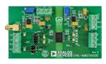
EVALUATION BOARD PHOTOGRAPH
Figure 1.
PLEASE SEE THE LAST PAGE FOR AN IMPORTANT
WARNING AND LEGAL TERMS AND CONDITIONS.
Rev. 0 | Page 1 of 16
�UG-997
EVAL-ADM2795EEBZ User Guide
TABLE OF CONTENTS
Features .............................................................................................. 1
IEC 61000-4-4 Electrical Fast Transients (EFT)............................5
Evaluation Kit Contents ................................................................... 1
IEC 61000-4-5 Surge .....................................................................6
General Description ......................................................................... 1
IEC 61000-4-6 Conducted RF Immunity ..................................7
Certified IEC EMC RS-485 Evaluation Board.............................. 1
IEC 61000-4-3 Radiated RF Immunity ......................................8
Evaluation Board Photograph ......................................................... 1
IEC 61000-4-8 Magnetic Immunity ...........................................8
Revision History ............................................................................... 2
±42 V Fault Protection .................................................................9
Evaluation Board Hardware Configuration .................................. 3
RS-485 Network Biasing and Termination ................................9
Test Setup ....................................................................................... 3
Passing EN 55022 Class B Radiated Emissions ......................... 10
Jumper Settings ............................................................................. 3
Evaluation Board Schematics........................................................ 12
Termination and Pull-Up/Pull-Down Resistors ...................... 4
Assembly Drawings and Board Layout ....................................... 14
Decoupling and Reservoir Capacitors ....................................... 4
Ordering Information .................................................................... 15
Board Internal Layer Thickness ................................................. 4
Bill of Materials ........................................................................... 15
IEC EMC Robust RS-485 Evaluation Board ............................. 4
IEC 61000-4-2 Electrostatic Discharge (ESD) .......................... 5
REVISION HISTORY
9/2016—Revision 0: Initial Version
Rev. 0 | Page 2 of 16
�EVAL-ADM2795EEBZ User Guide
UG-997
EVALUATION BOARD HARDWARE CONFIGURATION
TEST SETUP
JUMPER SETTINGS
The EVAL-ADM2795EEBZ evaluation board is shown in Figure 2
with the default jumper settings on LK1 and LK4 (driver and
receiver enabled), power connections on J5 and J2, input signal
connection on J3, and probes attached to RXD, TXD, A, and B
for a loopback test.
Use the jumpers on the EVAL-ADM2795EEBZ evaluation board
to configure the inputs on the ADM2795E (see Table 1). Do not
place multiple jumper blocks on LK1 and LK4 because the input
sources can short together. For each link, move a single jumper
block from one position to another, as specified in Table 1.
1.7V TO 5.5V
POWER
SUPPLY
OSCILLOSCOPE
VREG1 GND1 VDD1
J2
J5
SIGNAL
GENERATOR
VREG2
GND2
VDD1 GND1
TXD1
VDD2
A
B
C
D
TXD
DE
RE
TXD
RE
B
A
C
B
A
RXD
RXD
J3
DE
J1
B
A
GND2
3.3V OR 5V
POWER
SUPPLY
GND2
LK4
EVAL-ADM2795EEBZ REV B
14665-002
VDD2
GND2
LK1
Figure 2. Basic Operation of the Evaluation Board for the ADM2795E Robust 5 kV rms Isolated RS-485 Transceiver with Level 4 EMC and Full ±42 V Protected
Table 1. Jumper Configuration
Link
LK1
Connection
A
B
C
D
LK4
A
B
C
Description
Connects the driver enable input (DE) of the ADM2795E to VDD1. This setting enables the driver.
Connects the driver enable input (DE) of the ADM2795E to GND1. This setting disables the driver.
Connects the driver enable input (DE) of the ADM2795E to the J3-2 terminal block connector.
Connects the driver enable input (DE) of the ADM2795E to the receiver enable input (RE); that is, LK7 sets the input
for both RE and DE. This setting ensures that when the driver is enabled, the receiver is disabled, or when the driver is
disabled, the receiver is enabled.
Connects the receiver enable input (RE) of the ADM2795E to VDD1. This setting disables the receiver.
Connects the receiver enable input (RE) of the ADM2795E to GND1. This setting enables the receiver.
Connects the receiver enable input (RE) of the ADM2795E to the J3-3 terminal block connector.
Rev. 0 | Page 3 of 16
�UG-997
EVAL-ADM2795EEBZ User Guide
TERMINATION AND PULL-UP/PULL-DOWN
RESISTORS
BOARD INTERNAL LAYER THICKNESS
The EVAL-ADM2795EEBZ evaluation board includes a R1
footprint for fitting a termination resistor between the A and
the B driver outputs/receiver inputs. By default, the EVALADM2795EEBZ is not fitted with a 120 Ω resistor (R1) between
the A and B pins. If the EVAL-ADM2795EEBZ is connected to a
bus that is already terminated at both ends, remove this resistor.
For more information about proper termination, see the AN-960
Application Note, RS-485/RS-422 Circuit Implementation Guide.
Although the ADM2795E has a built-in receiver fail-safe for
the bus idle condition, there are footprints on the EVALADM2795EEBZ evaluation board for fitting the R6 pull-up
resistor to VDD2 on A, as well as the R7 pull-down resistor to
GND2 on B. These resistors can be fitted when the user connects to
other devices that require such external biasing resistors on the
bus. The exact value required for a 200 mV minimum differential
voltage in the bus idle condition depends on the VDD2 supply
voltage (for example, 960 Ω for 3.3 V and 1440 Ω for 5 V). For
more information about the bus idle fail-safe, see the AN-960
Application Note, RS-485/RS-422 Circuit Implementation Guide.
DECOUPLING AND RESERVOIR CAPACITORS
The EVAL-ADM2795EEBZ uses the following decoupling and
reservoir capacitors:
•
On the logic side of the EVAL-ADM2795EEBZ, the C5 and
C6 capacitors must be 10 µF tantalum and 100 nF ceramic
capacitors, respectively, and the C7 capacitor must not be
fitted.
• On the bus side of the EVAL-ADM2795EEBZ, the C3 and
C1 capacitors must be 10 µF tantalum and 100 nF ceramic
capacitors, respectively, and the C8 capacitor must not be
fitted. A 100 nF ceramic capacitor (C2) must also be
connected between Pin 12 and Pin 13.
Additional capacitors must be added for power regulation
circuits:
• The C10, C13, C14, and C19 10 µF tantalum capacitors
must be added to the VDD1 power regulation circuit.
• The C17 and C18 10 µF ceramic capacitors must be added
to the VDD2 power regulation circuit.
• The C12, C15, C16, and C20 100 nF ceramic capacitors
must be added to the power regulation circuits.
The EVAL-ADM2795EEBZ evaluation board consists of two
layers. The spacing between the top and bottom layer is 1.6 mm.
The EVAL-ADM2795EEBZ PCB has greater than 0.4 mm between
Layer 1 and Layer 2, meeting requirements for isolation standards
IEC 61010 Third Edition and IEC 60950, as described in the
AN-1109 Application Note, Recommendations for Control of
Radiated Emissions with iCoupler Devices.
IEC EMC ROBUST RS-485 EVALUATION BOARD
The EVAL-ADM2795EEBZ evaluation board has been lab tested
and certified to provide RS-485 A, B bus pin protection for the
following IEC system level standards and test levels:
•
•
•
Protection against IEC 61000-4-5 surge to ±4 kV
Protection against IEC 61000-4-4 EFT to ±2 kV
Protection against IEC 61000-4-2 ESD to ±8 kV for contact
and ±15 kV for air
• IEC 61000-4-6 conducted RF immunity to Level 3
(10 V/m rms)
The EVAL-ADM2795EEBZ was lab tested and confirmed to pass
HBM ESD to >±30 kV on the RS-485 A, B bus pins.
The EVAL-ADM2795EEBZ was lab tested and certified as follows
to a number of IEC standards showing the robust EMC immunity
provided by the isolation barrier:
•
•
•
•
Withstands IEC 61000-4-5 surge to ±4 kV
Withstands IEC 61000-4-4 EFT to ±2 kV
Withstands IEC 61000-4-2 ESD ±9 kV contact and ±8 kV air
IEC 61000-4-6 conducted RF immunity Level 3 (10 V/m)
The EVAL-ADM2795EEBZ evaluation board meets stringent
EMI emissions targets (EN55022 Class B) with minimal PCB
layout considerations. To achieve a 6 dB µV/m margin from
EN55022 Class B limits, a 120 pF, 0603 body size capacitor must
be added on the PCB trace connected to the RxD pin. The
EVAL-ADM2795EEBZ evaluation board also meets the following
immunity standards:
•
•
IEC 61000-4-3 radiated RF immunity Level 4 (30 V/m)
IEC 61000-4-8 magnetic field immunity Level 5 (100 A/m)
The EVAL-ADM2795EEBZ evaluation board can withstand high
voltage faults to ±42 V ac/dc peak on RS-485 A, B bus pins.
Rev. 0 | Page 4 of 16
�EVAL-ADM2795EEBZ User Guide
UG-997
IEC 61000-4-2 ELECTROSTATIC DISCHARGE (ESD)
IEC 61000-4-4 ELECTRICAL FAST TRANSIENTS (EFT)
The IEC 61000-4-2 ESD standard describes the tests using two
coupling methods: contact discharge and air gap discharge.
Contact discharge implies a direct contact between the discharge
gun and the unit under test. During air discharge testing, the
charged electrode of the discharge gun moves toward the unit
under test until a discharge occurs as an arc across the air gap.
The discharge gun does not make direct contact with the unit
under test. The ADM2795E data sheet provides additional
information on the IEC 61000-4-2 ESD standard, including test
waveforms. Figure 3 shows an example test setup where the
EVAL-ADM2795EEBZ PCB was tested to both contact and air
discharge IEC 61000-4-2 ESD. Testing was performed in normal
transceiver operation, with the ADM2795E clocking data at
2.5 Mbps. Testing was performed with the IEC ESD gun connected
to the Local Bus Ground 2 (GND2), and in this configuration,
Table 2 shows that the ADM2795E protects against IEC 61000-4-2
Level 4.
During IEC 61000-4-4 EFT testing, EFT fast burst transients
were coupled onto RS-485 communication lines using a
capacitive clamp, as shown in Figure 4. The IEC EFT clamp
edge was placed at 50 cm away from the equipment under test,
EUT (EVAL-ADM2795EEBZ). The EFT generator was setup for
both 5 kHz and 100 kHz repetitive EFT bursts. The ADM2795E
data sheet provides additional information on the IEC 61000-44 EFT standard, including test waveforms. Testing was
performed in normal transceiver operation, with the
ADM2795E clocking data at 2.5 Mbps.
In addition, testing was performed with an IEC ESD gun
connected to the logic side, Ground 1 (GND1). Testing to GND1
demonstrates the robustness of the ADM2795E isolation barrier.
The isolation barrier is capable of withstanding the IEC ESD test
levels as described in Table 2. Table 11 details the Class B
compliance of the ADM2795E to the IEC 61000-4-2 ESD.
With the IEC EFT clamp connected to GND2, the ADM2795E is
robust to IEC EFT transients and protects against the highest
level recognized in the Level 4standard, which defines a voltage
level of ±2 kV. With the IEC EFT clamp connected to GND1,
the ADM2795E is robust to IEC EFT transients and withstands
up to ±2 kV. Testing to GND1 demonstrates the robustness of
the ADM2795E isolation barrier. Table 3 summarizes the IEC
61000-4-4 EFT certified test results. Table 3 results are valid for
setup with or without an RS-485 cable shield connection to GND2.
Table 11 details the Class B compliance of the ADM2795E to
the IEC 61000-4-4 EFT.
ISOLATION
BARRIER
VDD1
VDD2
ISOLATION
BARRIER
VDD2
VDD1
VDD1
VDD2
VDD2
100nF
GND1
GND2
100nF
VDD1
100nF
GND1
GND2
100nF
ADM2795E
TxD
ADM2795E
DE
A
RE
B
IEC EFT
GENERATOR
5kHz, 100kHz
TxD
100nF
DE
A
RE
B
RxD
IEC ESD GUN1
GND1
100nF
GND2
RS-485
CABLE
RS-485
CABLE
SHIELD
IEC EFT CLAMP1
RxD
GND2
14665-003
1IEC
1IEC
ESD GUN GROUND RETURN PATH IS CONNECTED
TO EITHER GND1 OR GND2
EFT CLAMP GROUND RETURN PATH IS CONNECTED
TO EITHER GND1 OR GND2
Figure 4. IEC 61000-4-4 EFT Testing to GND1 or GND2
Figure 3. IEC 61000-4-2 ESD Testing to GND1 or GND2
Table 2. IEC 61000-4-2 ESD Certified Test Results
ESD Gun Connection Point
GND2
GND1
IEC 61000-4-2 Test Result
±15 kV for air and ±8 kV for contact, Level 4 protection
Withstands ±8 kV for air and ±9 kV for contact
Certified Result
Yes
Yes
Table 3. IEC 61000-4-4 EFT Certified Test Results
EFT Clamp Connection Point
GND2
GND1
IEC 61000-4-4 Test Result
±2 kV Level 4 protection
Withstands ±2 kV
Rev. 0 | Page 5 of 16
Certified Result
Yes
Yes
14665-004
GND1
�UG-997
EVAL-ADM2795EEBZ User Guide
IEC 61000-4-5 SURGE
ISOLATION
BARRIER
With the IEC surge generator connected to GND2, the
ADM2795E is robust to IEC 61000-4-5 events and protects
against the highest level recognized in the Level 4 standard,
which defines a peak voltage of ±4 kV.
VDD1
VDD2
VDD2
VDD1
100nF
GND1
100nF
GND2
100nF
TxD
ADM2795E
DE
A
RE
B
CD
GND2
COUPLING NETWORK
1IEC SURGE GENERATOR GROUND RETURN PATH IS CONNECTED
TO EITHER GND1 OR GND2
Figure 5. IEC 61000-4-5 Surge Testing to GND1 or GND2
With the IEC surge generator connected to GND1, the ADM2795E
is robust to IEC 61000-4-5 events and withstands up to ±4.0 kV.
Testing to GND1 demonstrates the robustness of the ADM2795E
isolation barrier. Table 4 summarizes the certified test results.
Table 11 details the Class B compliance of the ADM2795E to
the IEC 61000-4-5 surge when tested to GND2, and Class A
compliance of the ADM2795E to the IEC 61000-4-5 surge when
tested to GND1.
Table 4. IEC 61000-4-5 Surge Certified Test Results
Surge Generator Connection Point
GND2
GND1
IEC
SURGE
GENERATOR
80Ω
RxD
GND1
80Ω
14665-005
IEC 61000-4-5 surge testing involved using a coupling network
to couple the surge transient into the RS-485 A, B bus pins.
The coupling network for a half duplex RS-485 device consists
of an 80 Ω resistor on both the A and B lines and a coupling
device. The total parallel sum of the resistance is 40 Ω. The
coupling device (CD) can be capacitors, gas arrestors, clamping
devices, or any method that allows the EUT to function correctly
during the applied test. During the surge test, five positive
and five negative pulses were applied to the data ports with a
maximum time interval of one minute between each pulse.
Testing was performed in normal transceiver operation with the
ADM2795E clocking data at 2.5 Mbps. Figure 5 shows the test
setup for surge testing. The ADM2795E data sheet provides
additional information on the IEC 61000-4-5 surge, including
test waveforms.
IEC 61000-4-5 Test Result
±4 kV Level 4 protection
Withstands ±4 kV
Rev. 0 | Page 6 of 16
Certified Result
Yes
Yes
�EVAL-ADM2795EEBZ User Guide
UG-997
IEC 61000-4-6 CONDUCTED RF IMMUNITY
a communications cable between two EVAL-ADM2795EEBZ.
The ADM2795E was tested to Level 3, which is the highest test
level of 10 V. For all testing, the equipment and EUT setup is
described in Table 5 and Figure 6. For all tests, the IEC 61000-4-6
clamp was placed at the EVAL-ADM2795EEBZ EUT, and the
cable shield was either floating or earthed. The second EVALADM2795EEBZ (auxiliary equipment) was placed on the
network to terminate the communications bus. Table 6 shows
the test results where the EUT passed IEC 61000-4-6 to Level 3.
The IEC 61000-4-6 generator clamp was connected to either
GND1 or GND2 to provide a return current path for the IEC
61000-4-6 transient current.
The EVAL-ADM2795EEBZ was lab tested and certified to pass
IEC 61000-4-6 conducted RF immunity testing to Level 3
(10 V/m rms). The IEC 61000-4-6 conducted immunity test is
applicable to products that operate in environments where RF
fields are present, and where they are connected to the mains
power supplies or other networks (signal or control lines). The
source of conducted disturbances are electromagnetic fields,
emanating from RF transmitters that may act on the whole length
of cables connected to installed equipment. In the IEC 61000-4-6
test, the RF voltage swept and stepped from 150 kHz to 80 MHz.
The RF voltage was amplitude modulated 80% at 1 kHz. The RF
voltage was applied to the EUT (one EVAL-ADM2795EEBZ)
using a clamp, as specified in Table 6. The clamp was placed on
Table 11 details the Class A compliance of the ADM2795E to the
IEC 61000-4-6 conducted RF immunity.
IEC
61000-4-6
GENERATOR
ISOLATION
BARRIER
VDD1
VDD2
VDD2
ISOLATION
BARRIER
VDD1
VDD2
VDD2
VDD1
100nF
VDD1
GND1
100nF
GND2
100nF
100nF
100nF
GND1
100nF
GND2
ADM2795E
DE
EUT
RE
TxD
RS-485
CABLE
A
A
B
RxD
GND1
GND2
ADM2795E
AUXILIARY
EQUIPMENT
B
RS-485
CABLE
SHIELD
IEC
61000-4-6
CLAMP
GND1
DE
RE
RxD
GND2
GND1
1IEC SURGE GENERATOR GROUND RETURN PATH IS CONNECTED TO EITHER GND1 OR GND2
14665-006
TxD
Figure 6. IEC 61000-4-6 Conducted RF Immunity Example Test Setup
Table 5. IEC 61000-4-6 EUT Set Up and Equipment
Parameter
IEC 61000-4-6 Clamp
IEC 61000-4-6 Test Level
EUT
EUT Data Rate
EUT Power
Cable Between EUT
Cable Termination
Pass/Fail Criteria
Details
Schaffner KEMZ 801, placed at 30 cm away from the EUT
Level 3, 0.15 MHz to 100 MHz, 10 V/m rms, 80% amplitude modulated by a 1 kHz sinusoidal
EVAL-ADM2795EEBZ
2.5 Mbps
9 V battery at VDD1 and VDD2, regulated on EUT to 5 V
5 m, Unitronic ProfiBus, 22 American wire gauge (AWG)
120 Ω resistor at both cable ends
Pass: data at receiver with a pulse width distortion within 10% of mean
Table 6. IEC 61000-4-6 Conducted RF Immunity Certified Test Results
Clamp Location
30 cm from EUT
30 cm from EUT
30 cm from EUT
30 cm from EUT
Cable Shield
Floating
Earthed
Floating
Earthed
Current Return Path
GND1
GND1
GND2
GND2
Rev. 0 | Page 7 of 16
IEC 61000-4-6 Test Frequency (MHz)
0.15 to 80
0.15 to 80
0.15 to 80
0.15 to 80
Certified Result
Pass
Pass
Pass
Pass
�UG-997
EVAL-ADM2795EEBZ User Guide
IEC 61000-4-3 RADIATED RF IMMUNITY
IEC 61000-4-8 MAGNETIC IMMUNITY
Testing to IEC 61000-4-3 ensures that electronic equipment is
immune to commonly occurring radiated RF fields. Some
commonly occurring unintentional RF emitting devices in an
industrial application are electric motors and welders.
Testing to IEC 61000-4-8 ensures that electronic equipment is
immune to commonly occurring magnetic fields. The source of
magnetic fields in typical industrial communication applications is
a power line current or 50/60 Hz transformers in close proximity
to equipment.
In the IEC 61000-4-3 test, an antenna in a shielded anechoic
chamber using a precalibrated field, swept from 80 MHz to
2.7 GHz, generated a radiated RF field. The RF voltage was
amplitude modulated 80% at 1 kHz. Each face of the EUT was
subjected to vertical and horizontal polarizations.
In the IEC 61000-4-8 test, a controlled magnetic field of defined
field strength was produced by driving a large coil (induction
coil) with a test generator. The EUT was placed at the center of
the induction coil, subjecting the EUT to a magnetic field.
Figure 7 shows the IEC 61000-4-3 radiated RF immunity test
setup with the EUT (EVAL-ADM2795EEBZ) placed in an
anechoic chamber, powered with two 9 V batteries. The EVALADM2795EEBZ on-board regulators power VDD1 and VDD2
at 5 V. The EVAL-ADM2795EEBZ is loaded with a R1 termination
120 Ω resistance (see Figure 12) for the duration of the test.
A pattern generator provides 2.5 Mbps of data input to the
ADM2795E TxD pin. The ADM2795E receiver output (RxD)
was monitored with an oscilloscope.
The pass criteria is less than a 10% change in the bit width of
the RxD signal in the presence of the IEC 61000-4-3 radiated
RF field.
The EVAL-ADM2795EEBZ was tested and certified to pass the
IEC 61000-4-3 radiated RF immunity testing to Level 4 (30 V/m).
Level 4 is the highest level in the IEC 61000-4-3 standard. Table 11
details the Class A compliance of the ADM2795E to the IEC
61000-4-3 radiated RF immunity.
EUT
TESTED ON ALL FOUR SIDES
Figure 8 shows the IEC 61000-4-8 magnetic immunity test
setup with the EUT (EVAL-ADM2795EEBZ) placed in an
anechoic chamber, powered with two 9 V batteries. The EVALADM2795EEBZ on-board regulators power VDD1 and VDD2
at 5 V. The EVAL-ADM2795EEBZ is loaded with a R1 termination
120 Ω resistance (see Figure 12) for the duration of the test.
A pattern generator provides 2.5 Mbps of data input to the
ADM2795E TxD pin. The ADM2795E receiver output (RxD)
was monitored with an oscilloscope. The pass criteria is less
than a 10% change in the bit width of the RxD signal in the
presence of the IEC 61000-4-8 magnetic field.
The EVAL-ADM2795EEBZ was tested and certified to pass
IEC 61000-4-8 magnetic immunity testing to Level 5 (100 A/m).
Level 5 is the highest level specified in the IEC 61000-4-8
standard. Table 11 details the Class A compliance of the
ADM2795E to the IEC 61000-4-8 magnetic immunity.
ANECHOIC
CHAMBER
EUT
RF ABSORBING
MATERIAL
INDUCTION LOOP
VDD1
9V
BATTERY
EVAL-ADM2795EEBZ
VDD1
9V
BATTERY
VDD2
9V
BATTERY
TRANSMIT
ANTENNA
VDD2
9V
BATTERY
EVAL-ADM2795EEBZ
IEC 61000-4-8
TEST CURRENT
GENERATOR
EUT
EUT
ISOLATION
BARRIER
ISOLATION
BARRIER
ANTENNA AT
1 METER TO 3 METERS
FROM EUT
POWER MONITOR
AND AMPLIFIER
OSCILLOSCOPE MONITORING
RxD RECEIVER OUTPUT
PATTERN GENERATOR
TxD DRIVER INPUT
Figure 7. IEC 61000-4-3 Radiated RF Immunity Test Setup
Rev. 0 | Page 8 of 16
PATTERN GENERATOR
TxD DRIVER INPUT
Figure 8. IEC 61000-4-8 Magnetic Immunity Test Setup
14665-108
14665-107
OSCILLOSCOPE MONITORING
RxD RECEIVER OUTPUT
�EVAL-ADM2795EEBZ User Guide
UG-997
±42 V FAULT PROTECTION
RS-485 NETWORK BIASING AND TERMINATION
The ADM2795E is protected against high voltage miswire events
when it operates on a bus that does not have RS-485 termination or
bus biasing resistors installed. A typical miswire event is where
a high voltage 24 V ac/dc power supply is connected directly
to RS-485 bus pin connectors. The ADM2795E can withstand
miswiring faults of up to ±42 V peak on the RS-485 bus pins
with respect to GND2 without damage. Miswiring protection
is guaranteed on the ADM2795E RS-485 A, B bus pins and is
guaranteed in the case of a hot swap of connectors to the bus
pins. Table 7 and Table 8 provide a summary of the high voltage
miswire protection offered by the ADM2795E. The EVALADM2795EEBZ was tested with ±42 V dc and with ±24 V
± 20% rms, 50 Hz/60Hz, with both a hot plug and dc ramp
test waveforms. The test was performed in both powered and
unpowered/floating power supply cases, and at a range of different
states for the RS-485 TxD input and DE/RE enable pins. The
RS-485 bus pins survive a high voltage miswire from Pin A to
ground, from Pin B to ground, and between Pin A and Pin B.
For a high voltage miswire on the RS-485 A, B bus pins with
biasing and termination resistors installed, there is a current
path through the biasing network to the ADM2795E power
supply VDD2 pin. To protect the ADM2795E in this scenario, the
device has an integrated VDD2 protection circuit. The ADM2795E
is the only fault protected RS-485 device on the market that also
features protection for its power supply pin. This protection
means that the current path through the R1 pull-up resistor
does not cause damage to the VDD2 pin, although the pull-up
resistor itself can be damaged if it is not appropriately power
rated (see Figure 9). The R1 pull-up resistor, power rating
depends on the miswire voltage and the resistance value.
If there is a miswire between the A and the B pins in the Figure 9
bus setup, the ADM2795E is protected, but the RT bus termination
resistor can be damaged if not appropriately power rated. The
RT termination resistor, power rating depends on the miswire
voltage and the resistance value.
VDD2
VDD1
Table 7. Miswire Protection Table Abbreviations
Description
High level for logic pin
Low level for logic pin
On or off power supply state
DIGITAL ISOLATOR
RxD
RS-485
TRANSCEIVER
R1
390Ω
A
RE
EMC
PROTECTION
CICRUIT
DE
VDD1
X
X
X
X
VDD2
X
X
X
X
DE
H/L
H/L
H/L
H/L
Inputs
RE
H/L
H/L
H/L
H/L
TxD
H/L
H/L
H/L
H/L
VDD2
R
Table 8. High Voltage Miswire Protection
Supply
ADM2795E
Miswire Protection at
RS-485 Outputs Pins1, 2
−42 V dc ≤ VA ≤ +42 V dc
−42 V dc ≤ VB ≤ +42 V dc
−42 V ac ≤ VA ≤ +42 V ac
−42 V ac ≤ VB ≤ +42 V ac
B
R2
390Ω
D
TxD
B
A
RT
220Ω
GND2
GND1
ISOLATION
BARRIER
GND2
Figure 9. High Voltage Miswiring Protection for the ADM2795E with Bus
Termination and Biasing Resistors
This is the ac/dc peak miswire voltage between Pin A and GND2, or Pin B and
GND2, or between Pin A and Pin B.
2
VA refers to the voltage on Pin A, and VB refers to the voltage on Pin B.
1
Rev. 0 | Page 9 of 16
14129-007
Letter
H
L
X
�UG-997
EVAL-ADM2795EEBZ User Guide
80
The EVAL-ADM2795EEBZ passed the EN 55022 Class B
radiated emissions standard. The EVAL-ADM2795EEBZ was
configured and tested with 1.7 V VDD1 and 3.0 V VDD2 power
supplies, and it was also tested with 5.0 V VDD1 and 5.0 V
VDD2 power supplies. Testing was performed at a 2.5 Mbps
clock data on the TxD input. The RS-485 A, B bus pins were
loaded with a 120 Ω termination resistor. Testing was also
performed without a 120 Ω termination resistor.
70
60
50
EN55022
40
EN55022B
30
20
10
0
30M
14665-009
Measurements were done in a semianechoic chamber at 10 meters
within the 30 MHz to 2 GHz frequency range. Table 9 shows the
list of test equipment used. Figure 10 and Figure 11 show the
results of the worst case horizontal and vertical scans with 5.0 V
VDD1 and 5.0 V VDD2 power supplied to the ADM2795E, using
9 V batteries and on-board regulator circuitry, with data switching
at the 2.5 Mbps clock on TxD, and a 120 Ω termination resistor
installed at R1 on the EVAL-ADM2795EEBZ. Table 10 details
the certified results. The EVAL-ADM2795EEBZ evaluation board
meets the EN 55022 Class B emission standard with more than a
6 dB μV margin. To obtain a 6 dB μV margin, it is recommended
that a 120 pF, 0603 body size capacitor be added on the PCB trace
connected to the RxD pin. EN 55022 Class B certification
documents for the EVAL-ADM2795EEBZ evaluation board are
available upon request from Analog Devices, Inc.
QUASI PEAK LEVEL (dBµV/m)
PASSING EN 55022 CLASS B RADIATED EMISSIONS
100M
FREQUENCY (Hz)
1G
Figure 11. Worst Case Vertical Emissions, VDD1 = VDD2 = 5 V
Table 9. Radiated Emissions Test Equipment
Instrument
Measuring Receiver
Bilog Antenna
Spectrum Analyzer
Horn Antenna
Manufacturer
Rohde & Schwarz
Chase
Agilent
EMCO
Model
ESVS30
Not applicable
E4408B
EMCO 3115
80
QUASI PEAK LEVEL (dBµV/m)
70
60
50
EN55022
40
EN55022B
30
20
0
30M
14665-008
10
100M
FREQUENCY (Hz)
1G
Figure 10. Worst Case Horizontal Emissions, VDD1 = VDD2 = 5.0 V
Table 10. EVAL-ADM2795EEBZ 5.0 V VDD1/VDD2 EN 55022 Certified Test Results
Frequency (MHz)
46.272
48.776
48.772
65.132
Quasipeak Level dB (μV/m)
23.9
23.7
16.8
16
EN55022 Class B dB (μV/m)
30
30
30
30
Rev. 0 | Page 10 of 16
Antenna Position
Vertical
Vertical
Horizontal
Horizontal
Pass/Fail
Pass, with 6.1 dB (μV/m) margin
Pass, with 6.3 dB (μV/m) margin
Pass, with 13.2 dB (μV/m) margin
Pass, with 14.0 dB (μV/m) margin
�EVAL-ADM2795EEBZ User Guide
UG-997
Table 11 summarizes the EVAL-ADM2795EEBZ performance
and classification achieved for the noted IEC system level EMC
standards.
The performance that corresponds to each classification follows:
•
•
•
•
Class A means normal operation.
Class B means a temporary loss of performance (bit errors).
Class C means that the system needs a reset.
Class D means a permanent loss of function.
Table 11. EVAL-ADM2795EEBZ Performance and Classification Achieved
Test
IEC 61000-4-5 Surge
IEC 61000-4-4 Electrical Fast Transient (EFT)
IEC 61000-4-2 Electrostatic Discharge (ESD)
IEC 61000-4-6 Conducted RF Immunity
IEC 61000-4-3 Radiated RF Immunity
IEC 61000-4-8 Magnetic Immunity
Ground Connection
GND1
GND2
GND1
GND2
GND1
GND2
GND1
GND2
GND2
GND2
Rev. 0 | Page 11 of 16
Classification
Class A
Class B
Class B
Class B
Class B
Class B
Class A
Class A
Class A
Class A
Highest Pass Level
±4 kV
±4 kV
±2 kV
±2 kV
±8 kV (air), ±9 kV (contact)
±15 kV (air), ±8 kV (contact)
10 V/m
10 V/m
30 V/m
100 A/m
�Rev. 0 | Page 12 of 16
J3-4
J3-3
VDD1
GND1
C
B
A
LK4
D
C
B
LK1
A
+
C5
10µF
VDD1
GND1
GND1 _2
SMA
TXD1
GND1
GND1 _1
RXD
RE
DE
TXD
100nF
GND1
C11
VDD1
Figure 12. Schematics of the EVAL-ADM2795EEBZ Evaluation Board, Page 1
GND1
1 20pF
GND1
GND1
NC
RXD
RE
DE
TXD
GND1
VDD1
U1
VDD2
GND2
GND2
A
GND2
VDD2
B
GND2
ADM2 7 95EBRWZ
8
7
6
5
4
3
2
1
Ω
J3-2
J3-1
GND1
100nF
C6
9
10
11
12
13
14
15
16
GND2
VDD2
C1
1 0 0nF
VDD2
J2-1
C2
100nF
GND2
A
B
GND2
1 0uF
GND2_2
C8
100nF
C3
+
J5-2
GND1 _3
J5-1
C7
VDD1
J2-2
1.2kΩ* DO NOT FIT
R6
1.2kΩ* DO NOT FIT
R7
VDD2
GND2
GND2
R1
120Ω* DO NOT FIT
J1-3
J1-2
J1-1
UG-997
EVAL-ADM2795EEBZ User Guide
EVALUATION BOARD SCHEMATICS
14665-010
�EVAL-ADM2795EEBZ User Guide
UG-997
T93 _POT
R2
A
B
C
1
R4
2
7 1 .5kΩ
R5
2 0 0kΩ
GND1
3
U3
R15
1
0Ω* DO NOT FIT
2
VDD1
3
+
4
C20
1 0 0nF
C10
10µF
DD
OUT
6
SET
GND
0Ω
J5-3
7
LBO
LBI
R9
8
IN
5
SHDN
+
C12
C18
100nF
1 0µF
C19
10µF
ADP6 6 7ARZ
GND1
GND1
T9 3 _POT
R11
A
B
C
1
R12
2
240kΩ
R13
200kΩ
3
GND2
U2
R10
0Ω* DO NOT FIT
1
2
VDD2
3
C13
1 0µF
4
IN
OUT
LBO
LBI
SET
GND
SHDN
R14
8
0Ω
J2-3
7
6
5
C15
C17
100nF
10µF
+
C14
10µF
ADP66 7ARZ
GND2
GND2
Figure 13. Schematics of the EVAL-ADM2795EEBZ Evaluation Board, Page 2
Rev. 0 | Page 13 of 16
14665-011
+
C16
100nF
DD
�UG-997
EVAL-ADM2795EEBZ User Guide
14665-012
ASSEMBLY DRAWINGS AND BOARD LAYOUT
14665-013
Figure 14. EVAL-ADM2795EEBZ Evaluation Board Silkscreen
14665-014
Figure 15. EVAL-ADM2795EEBZ Evaluation Board Top Layer
Figure 16. EVAL-ADM2795EEBZ Evaluation Board Bottom Layer
Rev. 0 | Page 14 of 16
�EVAL-ADM2795EEBZ User Guide
UG-997
ORDERING INFORMATION
BILL OF MATERIALS
Table 12.
Quantity
3
2
2
4
1
4
2
3
1
2
1
1
1
2
1
2
2
2
2
1
6
5
2
1
1
Reference Designator
C1, C2, C6
C3, C5
C7, C8
C10, C13, C14, C19
C11
C12, C15, C16, C20
C17, C18
J1, J2, J5
J3
J4, J6
LK1
LK4
R1
R2, R11
R4
R5, R13
R6, R7
R9, R14
R10, R15
R12
RXD, RE, DE, TXD, A, B
GND1_1, GND1_2,
GND1_3, GND2_1,
GND2_2,
GND1, GND 2
TXD1
U1
2
2
U2
VDD1, VDD2
Description
Capacitors, size 0603, 100 nF
Capacitors, tantalum, Case B, 10 µF
Capacitors, size 0603, 100 nF
Capacitors, tantalum, Case C, 10 µF
Capacitor, size 0603, 120 pF
Capacitors, size 0805, 100 nF
Capacitors, size 0805, 10 µF
CON\POWER3, 3-pin terminal blocks
CON\POWER4, 4-pin terminal block
CON\POWER2, 2-pin terminal blocks
8-pin (4 × 2), 2.54 mm header and shorting block
6-pin (3 × 2), 2.54 mm header and shorting block
Resistor, 120 Ω, size 0805 (not inserted)
Trimmer potentiometers
Resistor, 71.5 kΩ, size 0805
Resistors, 200 kΩ, size 0603
Resistors, 1.2 kΩ, size 0805 (not inserted)
Resistors, 0 Ω, size 0805
Resistors, 0 Ω, size 0603 (not inserted)
Resistor, 240 kΩ, size 0603
Test points, yellow
Test points, yellow
Supplier
AVX
KEMET
AVX
KEMET
AVX
Multicomp
AVX
Camden
Lumberg
Lumberg
Harwin
Harwin
Welwyn
Vishay
Welwyn
Bourns
Panasonic
Welwyn
Multicomp
Vishay
Vero
Vero
Device No.
06033C104JAT2A
B45196H3106K209
06033C104JAT2A
B45196E3106K309
0201YC121KAT2A
MC0805F104Z160CT
08056C106KAT2A
CTB5000/3
KRM 04
KRM 02
M20-9953646
M20-9983646
WCR0805-120RFI
T93YB504KT20
MC0063W0603171K5
CR0603-FX-2003ELF
ERA6AEB122V
WCR0805-R005JI
MC0063W06030R
CRCW0603240KFKEA
20-313140
20-313140
Test points, black
RH SMA connector
Isolated Level 4 EMC and 24 V supply fault
protected RS-485 transceiver
5 V fixed, adjustable voltage regulator
Test points, red
Vero
TE Connectivity
Analog Devices
20-2137
5-1814400-1
ADM2795EBRWZ
Analog Devices
Vero
ADP667ARZ
20-313137
Rev. 0 | Page 15 of 16
�UG-997
EVAL-ADM2795EEBZ User Guide
NOTES
ESD Caution
ESD (electrostatic discharge) sensitive device. Charged devices and circuit boards can discharge without detection. Although this product features patented or proprietary protection
circuitry, damage may occur on devices subjected to high energy ESD. Therefore, proper ESD precautions should be taken to avoid performance degradation or loss of functionality.
Legal Terms and Conditions
By using the evaluation board discussed herein (together with any tools, components documentation or support materials, the “Evaluation Board”), you are agreeing to be bound by the terms and conditions
set forth below (“Agreement”) unless you have purchased the Evaluation Board, in which case the Analog Devices Standard Terms and Conditions of Sale shall govern. Do not use the Evaluation Board until you
have read and agreed to the Agreement. Your use of the Evaluation Board shall signify your acceptance of the Agreement. This Agreement is made by and between you (“Customer”) and Analog Devices, Inc.
(“ADI”), with its principal place of business at One Technology Way, Norwood, MA 02062, USA. Subject to the terms and conditions of the Agreement, ADI hereby grants to Customer a free, limited, personal,
temporary, non-exclusive, non-sublicensable, non-transferable license to use the Evaluation Board FOR EVALUATION PURPOSES ONLY. Customer understands and agrees that the Evaluation Board is provided
for the sole and exclusive purpose referenced above, and agrees not to use the Evaluation Board for any other purpose. Furthermore, the license granted is expressly made subject to the following additional
limitations: Customer shall not (i) rent, lease, display, sell, transfer, assign, sublicense, or distribute the Evaluation Board; and (ii) permit any Third Party to access the Evaluation Board. As used herein, the term
“Third Party” includes any entity other than ADI, Customer, their employees, affiliates and in-house consultants. The Evaluation Board is NOT sold to Customer; all rights not expressly granted herein, including
ownership of the Evaluation Board, are reserved by ADI. CONFIDENTIALITY. This Agreement and the Evaluation Board shall all be considered the confidential and proprietary information of ADI. Customer may
not disclose or transfer any portion of the Evaluation Board to any other party for any reason. Upon discontinuation of use of the Evaluation Board or termination of this Agreement, Customer agrees to
promptly return the Evaluation Board to ADI. ADDITIONAL RESTRICTIONS. Customer may not disassemble, decompile or reverse engineer chips on the Evaluation Board. Customer shall inform ADI of any
occurred damages or any modifications or alterations it makes to the Evaluation Board, including but not limited to soldering or any other activity that affects the material content of the Evaluation Board.
Modifications to the Evaluation Board must comply with applicable law, including but not limited to the RoHS Directive. TERMINATION. ADI may terminate this Agreement at any time upon giving written notice
to Customer. Customer agrees to return to ADI the Evaluation Board at that time. LIMITATION OF LIABILITY. THE EVALUATION BOARD PROVIDED HEREUNDER IS PROVIDED “AS IS” AND ADI MAKES NO
WARRANTIES OR REPRESENTATIONS OF ANY KIND WITH RESPECT TO IT. ADI SPECIFICALLY DISCLAIMS ANY REPRESENTATIONS, ENDORSEMENTS, GUARANTEES, OR WARRANTIES, EXPRESS OR IMPLIED, RELATED
TO THE EVALUATION BOARD INCLUDING, BUT NOT LIMITED TO, THE IMPLIED WARRANTY OF MERCHANTABILITY, TITLE, FITNESS FOR A PARTICULAR PURPOSE OR NONINFRINGEMENT OF INTELLECTUAL
PROPERTY RIGHTS. IN NO EVENT WILL ADI AND ITS LICENSORS BE LIABLE FOR ANY INCIDENTAL, SPECIAL, INDIRECT, OR CONSEQUENTIAL DAMAGES RESULTING FROM CUSTOMER’S POSSESSION OR USE OF
THE EVALUATION BOARD, INCLUDING BUT NOT LIMITED TO LOST PROFITS, DELAY COSTS, LABOR COSTS OR LOSS OF GOODWILL. ADI’S TOTAL LIABILITY FROM ANY AND ALL CAUSES SHALL BE LIMITED TO THE
AMOUNT OF ONE HUNDRED US DOLLARS ($100.00). EXPORT. Customer agrees that it will not directly or indirectly export the Evaluation Board to another country, and that it will comply with all applicable
United States federal laws and regulations relating to exports. GOVERNING LAW. This Agreement shall be governed by and construed in accordance with the substantive laws of the Commonwealth of
Massachusetts (excluding conflict of law rules). Any legal action regarding this Agreement will be heard in the state or federal courts having jurisdiction in Suffolk County, Massachusetts, and Customer hereby
submits to the personal jurisdiction and venue of such courts. The United Nations Convention on Contracts for the International Sale of Goods shall not apply to this Agreement and is expressly disclaimed.
©2016 Analog Devices, Inc. All rights reserved. Trademarks and
registered trademarks are the property of their respective owners.
UG14665-0-9/16(0)
Rev. 0 | Page 16 of 16
�


 工商网监
湘ICP备2023018690号
工商网监
湘ICP备2023018690号

