10 W, GaN Power Amplifier,
2.7 GHz to 3.8 GHz
HMC1114
Data Sheet
FUNCTIONAL BLOCK DIAGRAM
Extended battery operation for public mobile radios
Power amplifier stage for wireless infrastructure
Test and measurement equipment
Commercial and military radars
General-purpose transmitter amplification
GND
GND
VDD1
GND
GND
VDD2
VDD2
GND
32
31
30
29
28
27
26
25
GND
GND
GND
RFIN
RFIN
GND
GND
GND
1
2
3
4
5
6
7
8
24
23
22
21
20
19
18
17
GND
GND
GND
RFOUT
RFOUT
GND
GND
GND
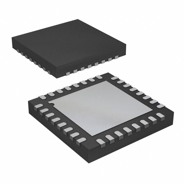
PACKAGE
BASE
13530-001
APPLICATIONS
HMC1114
9
10
11
12
13
14
15
16
High saturated output power (PSAT): 41.5 dBm typical
High small signal gain: 35 dB typical
High power gain for saturated output power: 25.5 dB typical
Bandwidth: 2.7 GHz to 3.8 GHz
High power added efficiency (PAE): 54% typical
High output IP3: 44 dBm typical
Supply voltage: VDD = 28 V at 150 mA
32-lead, 5 mm × 5 mm LFCSP_CAV package
GND
VGG1
GND
GND
VGG2
GND
GND
GND
FEATURES
Figure 1.
GENERAL DESCRIPTION
The HMC1114 is a gallium nitride (GaN), broadband power
amplifier, delivering 10 W with more than 50% power added
efficiency (PAE) across a bandwidth of 2.7 GHz to 3.8 GHz. The
HMC1114 provides ±0.5 dB gain flatness.
Rev. A
The HMC1114 is ideal for pulsed or continuous wave (CW)
applications such as wireless infrastructure, radar, public mobile
radio, and general-purpose amplification.
The HMC1114 is housed in a compact LFCSP_CAV package.
Document Feedback
Information furnished by Analog Devices is believed to be accurate and reliable. However, no
responsibility is assumed by Analog Devices for its use, nor for any infringements of patents or other
rights of third parties that may result from its use. Specifications subject to change without notice. No
license is granted by implication or otherwise under any patent or patent rights of Analog Devices.
Trademarks and registered trademarks are the property of their respective owners.
One Technology Way, P.O. Box 9106, Norwood, MA 02062-9106, U.S.A.
Tel: 781.329.4700 ©2016–2017 Analog Devices, Inc. All rights reserved.
Technical Support
www.analog.com
�HMC1114
Data Sheet
TABLE OF CONTENTS
Features .............................................................................................. 1
Interface Schematics .....................................................................5
Applications ....................................................................................... 1
Typical Performance Characteristics ..............................................6
Functional Block Diagram .............................................................. 1
Theory of Operation ...................................................................... 12
General Description ......................................................................... 1
Applications Information .............................................................. 13
Revision History ............................................................................... 2
Recommended Bias Sequence .................................................. 13
Specifications..................................................................................... 3
Typical Application Circuit ....................................................... 13
Electrical Specifications ............................................................... 3
Evaluation Printed Circuit Board (PCB) ..................................... 14
Total Supply Current by VDD ....................................................... 3
Bill of Materials ........................................................................... 14
Absolute Maximum Ratings ............................................................ 4
Outline Dimensions ....................................................................... 15
ESD Caution .................................................................................. 4
Ordering Guide .......................................................................... 15
Pin Configuration and Function Descriptions ............................. 5
REVISION HISTORY
3/2017—Rev. 0 to Rev. A
Changed EVL1HMC1114LP5D to
EV1HMC1114LP5D ..................................................... Throughout
Changes to Ordering Guide .......................................................... 15
9/2016—Revision 0: Initial Version
Rev. A | Page 2 of 15
�Data Sheet
HMC1114
SPECIFICATIONS
ELECTRICAL SPECIFICATIONS
TA = 25°C, VDD = 28 V, IDQ = 150 mA, frequency range = 2.7 GHz to 3.2 GHz, unless otherwise noted.
Table 1.
Parameter
FREQUENCY RANGE
GAIN
Small Signal Gain
Gain Flatness
Power Gain for 4 dB Compression
Power Gain for Saturated Output Power
RETURN LOSS
Input
Output
POWER
Output Power for 4 dB Compression
Saturated Output Power
Power Added Efficiency
OUTPUT THIRD-ORDER INTERCEPT
TARGET QUIESCENT CURRENT
Symbol
Min
2.7
Typ
32
35
±0.5
29
25.5
dB
dB
dB
dB
14
11
dB
dB
39
41.5
54
44
150
dBm
dBm
%
Measurement taken at PIN = 16 dBm
mA
Measurement taken at POUT/tone = 30 dBm
Adjust the gate control voltage (VGG1, VGG2) between
−8 V and 0 V to achieve an IDQ = 150 mA typical
P4dB
PSAT
PAE
IP3
IDQ
Max
3.2
Unit
GHz
Test Conditions/Comments
Measurement taken at PIN = 16 dBm
TA = 25°C, VDD = 28 V, IDQ = 150 mA, frequency range = 3.2 GHz to 3.8 GHz, unless otherwise noted.
Table 2.
Parameter
FREQUENCY RANGE
GAIN
Small Signal Gain
Gain Flatness
Power Gain for 4 dB Compression
Power Gain for Saturated Output Power
RETURN LOSS
Input
Output
POWER
Output Power for 4 dB Compression
Saturated Output Power
Power Added Efficiency
OUTPUT THIRD-ORDER INTERCEPT
TARGET QUIESCENT CURRENT
Symbol
P4dB
PSAT
PAE
IP3
IDQ
Min
3.2
Typ
Max
3.8
Unit
GHz
Test Conditions/Comments
29
32
±1
28
25
dB
dB
dB
dB
25
9
dB
dB
40
40.5
53
44
150
dBm
dBm
%
Measurement taken at PIN = 16 dBm
mA
Measurement taken at POUT/tone = 30 dBm
Adjust the gate control voltage (VGG1, VGG2) between
−8 V and 0 V to achieve an IDQ = 150 mA typical
Measurement taken at PIN = 16 dBm
TOTAL SUPPLY CURRENT BY VDD
Table 3.
Parameter
SUPPLY CURRENT
VDD = 25 V
VDD = 28 V
VDD = 32 V
Symbol
IDQ
Min
Typ
150
150
150
Max
Unit
mA
mA
mA
Rev. A | Page 3 of 15
Test Conditions/Comments
Adjust VGG1, VGG2 to achieve an IDQ = 150 mA typical
�HMC1114
Data Sheet
ABSOLUTE MAXIMUM RATINGS
Table 4.
Parameter
Drain Bias Voltage (VDD1, VDD2)
Gate Bias Voltage (VGG1, VGG2)
RF Input Power (RFIN)
Maximum Forward Gate Current
Continuous Power Dissipation, PDISS (TA = 85°C,
Derate 227 mW/°C Above 120°C)
Thermal Resistance, Junction to Back of Paddle
Channel Temperature
Maximum Peak Reflow Temperature (MSL3)1
Storage Temperature Range
Operating Temperature Range
ESD Sensitivity (Human Body Model)
1
Rating
35 V dc
−8 V to 0 V dc
30 dBm
4 mA
24 W
4.4°C/W
225°C
260°C
−40°C to +125°C
−40°C to +85°C
Class 1A,
passed 250 V
Stresses at or above those listed under Absolute Maximum
Ratings may cause permanent damage to the product. This is a
stress rating only; functional operation of the product at these
or any other conditions above those indicated in the operational
section of this specification is not implied. Operation beyond
the maximum operating conditions for extended periods may
affect product reliability.
ESD CAUTION
See the Ordering Guide section.
Rev. A | Page 4 of 15
�Data Sheet
HMC1114
32
31
30
29
28
27
26
25
GND
GND
VDD1
GND
GND
VDD2
VDD2
GND
PIN CONFIGURATION AND FUNCTION DESCRIPTIONS
1
2
3
4
5
6
7
8
HMC1114
TOP VIEW
(Not to Scale)
24
23
22
21
20
19
18
17
GND
GND
GND
RFOUT
RFOUT
GND
GND
GND
NOTES
1. EXPOSED PAD. EXPOSED PAD MUST
BE CONNECTED TO RF/DC GROUND.
13530-002
GND
VGG1
GND
GND
VGG2
GND
GND
GND
9
10
11
12
13
14
15
16
GND
GND
GND
RFIN
RFIN
GND
GND
GND
Figure 2. Pin Configuration
Table 5. Pin Function Descriptions
Pin No.
1 to 3, 6 to 9, 11, 12, 14 to
19, 22 to 25, 28, 29, 31, 32
4, 5
Mnemonic
GND
10, 13
VGG1, VGG2
20, 21
RFOUT
26, 27, 30
VDD1, VDD2
RFIN
EPAD
Description
Ground. These pins and the package bottom (EPAD) must be connected to RF/dc ground. See
Figure 3 for the GND interface schematic.
RF Input. These pins are dc-coupled and matched to 50 Ω. See Figure 4 for the RFIN interface
schematic.
Gate Control Voltage Pins. External bypass capacitors of 1 μF and 10 μF are required. See
Figure 5 for the VGG1 and VGG2 interface schematic.
RF Output. These pins are ac-coupled and matched to 50 Ω. See Figure 6 for the RFOUT
interface schematic.
Drain Bias Pins for the Amplifier. External bypass capacitors of 100 pF, 1 μF, and 10 μF are
required. See Figure 7 for the VDD1 and VDD2 interface schematic.
Exposed Pad. The exposed pad must be connected to RF/dc ground.
RFOUT
Figure 3. GND Interface
13530-006
GND
13530-003
INTERFACE SCHEMATICS
Figure 6. RFOUT Interface
VDD1 , VDD2
13530-004
13530-007
RFIN
Figure 4. RFIN Interface
Figure 7. VDD1 and VDD2 Interface
13530-005
VGG1, VGG2
Figure 5. VGG1 and VGG2 Interface
Rev. A | Page 5 of 15
�HMC1114
Data Sheet
TYPICAL PERFORMANCE CHARACTERISTICS
40
40
30
36
S22
S21
S11
10
GAIN (dB)
RESPONSE (dB)
20
0
–10
–20
32
+85°C
+25°C
–40°C
28
24
2.25
2.50
2.75
3.00
3.25
3.50
3.75
4.00
4.25
4.50
FREQUENCY (GHz)
20
2.6
13530-008
–40
2.00
2.8
3.0
3.2
3.4
3.6
3.8
4.0
FREQUENCY (GHz)
Figure 8. Response (Gain and Return Loss) vs. Frequency
13530-011
–30
Figure 11. Gain vs. Frequency at Various Temperatures
0
0
OUTPUT RETURN LOSS (dB)
–5
INPUT RETURN LOSS (dB)
–10
–15
–20
–25
+85°C
+25°C
–40°C
–30
–5
–10
+85°C
+25°C
–40°C
–15
2.8
3.0
3.2
3.4
3.6
3.8
4.0
FREQUENCY (GHz)
Figure 9. Input Return Loss vs. Frequency at Various Temperatures
36
36
32
32
GAIN (dB)
40
32V
28V
25V
20V
3.2
3.4
3.6
3.8
4.0
300mA
225mA
150mA
100mA
28
2.8
3.0
3.2
3.4
3.6
3.8
FREQUENCY (GHz)
4.0
Figure 10. Gain vs. Frequency at Various Supply Voltages
20
2.6
2.8
3.0
3.2
3.4
3.6
3.8
FREQUENCY (GHz)
Figure 13. Gain vs. Frequency at Various Supply Currents
Rev. A | Page 6 of 15
4.0
13530-013
24
24
20
2.6
3.0
Figure 12. Output Return Loss vs. Frequency at Various Temperatures
40
28
2.8
FREQUENCY (GHz)
13530-010
GAIN (dB)
–20
2.6
13530-009
–40
2.6
13530-012
–35
�HMC1114
44
42
42
40
40
P4dB (dBm)
44
36
34
32
32
2.8
3.0
3.2
3.4
3.6
3.8
4.0
FREQUENCY (GHz)
30
2.6
44
42
42
40
40
38
32V
28V
25V
20V
34
3.4
3.6
3.8
4.0
38
+85°C
+25°C
–40°C
36
3.0
3.2
3.4
3.6
3.8
4.0
30
2.6
13530-015
2.8
42
42
40
40
P4dB (dBm)
44
32V
28V
25V
20V
34
3.2
3.4
3.6
3.8
4.0
Figure 18. Saturated Output Power (PSAT) vs. Frequency at Various
Temperatures, Measurement Taken at PIN = 16 dBm
44
36
3.0
FREQUENCY (GHz)
Figure 15. Output Power for 4 dB Compression (P4dB) vs. Frequency at
Various Supply Voltages
38
2.8
13530-018
32
FREQUENCY (GHz)
38
300mA
225mA
150mA
100mA
36
34
3.0
3.2
3.4
FREQUENCY (GHz)
3.6
3.8
4.0
30
2.6
13530-016
2.8
Figure 16. Saturated Output Power (PSAT) vs. Frequency at Various Supply
Voltages, Measurement Taken at PIN = 16 dBm
2.8
3.0
3.2
3.4
FREQUENCY (GHz)
3.6
3.8
4.0
13530-019
32
32
30
2.6
3.2
34
32
30
2.6
3.0
Figure 17. Output Power for 4 dB Compression (P4dB) vs. Frequency at
Various Temperatures
44
36
2.8
FREQUENCY (GHz)
PSAT (dBm)
P4dB (dBm)
Figure 14. Output Power (POUT) vs. Frequency,
Measurement Taken at PIN = 16 dBm
+85°C
+25°C
–40°C
36
34
30
2.6
PSAT (dBm)
38
13530-017
P1dB
P4dB
PSAT AT PIN = 16dBm
38
13530-014
POUT (dBm)
Data Sheet
Figure 19. Output Power for 4 dB Compression (P4dB) vs. Frequency at
Various Supply Currents
Rev. A | Page 7 of 15
�HMC1114
Data Sheet
44
50
42
48
46
OUTPUT IP3 (dBm)
38
300mA
225mA
150mA
100mA
36
34
3.2
3.4
3.6
3.8
4.0
34
2.6
48
46
46
OUTPUT IP3 (dBm)
48
40
+85°C
+25°C
–40°C
38
44
42
300mA
225mA
150mA
100mA
40
38
36
3.0
3.2
3.4
3.6
3.8
34
2.6
13530-021
2.8
Figure 21. Output Third-Order Intercept (IP3) vs. Frequency at Various
Temperatures, POUT/Tone = 30 dBm
2.8
3.0
3.2
3.4
3.8
Figure 24. Output Third-Order Intercept (IP3) vs. Frequency at Various Supply
Currents, POUT/Tone = 30 dBm
35
50
33
3.8GHz
3.25GHz
2.7GHz
45
31
40
OUTPUT IM3 (dBc)
29
27
25
23
P1dB
P4dB
PSAT AT PIN = 16dBm
21
35
30
25
20
19
15
17
2.8
3.0
3.2
3.4
3.6
FREQUENCY (GHz)
3.8
4.0
13530-022
POWER GAIN (dB)
3.6
FREQUENCY (GHz)
13530-024
36
FREQUENCY (GHz)
15
2.6
3.8
3.6
Figure 23. Output Third-Order Intercept (IP3) vs. Frequency at Various Supply
Voltages, POUT/Tone = 30 dBm
50
42
3.4
3.2
3.0
FREQUENCY (GHz)
50
44
2.8
13530-023
3.0
13530-020
2.8
Figure 20. Saturated Output Power (PSAT) vs. Frequency at Various Supply
Currents, Measurement Taken at PIN = 16 dBm
34
2.6
32V
28V
25V
20V
40
36
FREQUENCY (GHz)
OUTPUT IP3 (dBm)
42
38
32
30
2.6
44
10
15
17
19
21
23
25
27
29
31
33
POUT /TONE (dBm)
Figure 25. Output Third-Order Intermodulation (IM3) vs.
POUT/Tone at VDD = 20 V
Figure 22. Power Gain vs. Frequency
Rev. A | Page 8 of 15
35
13530-025
PSAT (dBm)
40
�Data Sheet
HMC1114
50
3.8GHz
3.25GHz
2.7GHz
OUTPUT IM3 (dBc)
40
35
30
25
30
25
20
15
15
17
19
21
23
25
29
27
31
33
35
POUT /TONE (dBm)
10
15
17
19
21
23
25
27
29
31
Figure 26. Output Third-Order Intermodulation (IM3) vs. POUT/Tone at VDD = 25 V
60
35
30
25
20
1000
POUT
GAIN
PAE
IDD
50
POUT (dBm), GAIN (dB), PAE (%)
3.8GHz
3.25GHz
2.7GHz
40
900
800
700
40
600
500
30
400
300
20
200
15
100
21
23
25
29
27
31
33
35
POUT /TONE (dBm)
30
600
IDD (mA)
1050
750
450
20
20
POUT
GAIN
PAE
IDD
50
POUT (dBm), GAIN (dB), PAE (%)
1200
900
16
300
900
800
700
40
600
500
400
30
300
20
200
100
150
10
–4
0
4
8
12
16
20
0
24
1000
1350
40
12
60
0
24
10
–4
13530-027
POUT (dBm), GAIN (dB), PAE (%)
50
8
Figure 30. Output Power (POUT), Gain, Power Added Efficiency (PAE), and
Supply Current (IDD) vs. Input Power at 3.2 GHz
1500
POUT
GAIN
PAE
IDD
4
INPUT POWER (dBm)
Figure 27. Output Third-Order Intermodulation (IM3) vs. POUT/Tone at VDD = 28 V
60
0
13530-030
19
IDD (mA)
17
10
–4
13530-026
10
15
35
Figure 29. Output Third-Order Intermodulation (IM3) vs. POUT/Tone at VDD = 32 V
50
45
33
POUT /TONE (dBm)
INPUT POWER (dBm)
Figure 28. Output Power (POUT), Gain, Power Added Efficiency (PAE), and
Supply Current (IDD) vs. Input Power at 2.7 GHz
0
4
8
12
16
20
0
24
INPUT POWER (dBm)
Figure 31. Output Power (POUT), Gain, Power Added Efficiency (PAE), and
Supply Current (IDD) vs. Input Power at 3.8 GHz
Rev. A | Page 9 of 15
13530-031
10
15
OUTPUT IM3 (dBc)
35
20
13530-028
OUTPUT IM3 (dBc)
40
3.8GHz
3.25GHz
2.7GHz
45
IDD (mA)
45
13530-029
50
�HMC1114
Data Sheet
45
REVERSE ISOLATION (dB)
GAIN (dB), P4dB (dBm), PSAT (dBm)
+85°C
+25°C
–40°C
–10
–20
–30
–40
–50
–70
2.6
2.8
3.0
3.2
3.4
3.6
3.8
4.0
FREQUENCY (GHz)
35
30
P1dB
P4dB
PSAT AT PIN = 16dBm
25
20
24
13530-032
–60
40
25
Figure 32. Reverse Isolation vs. Frequency at Various Temperatures
27
28
Figure 35. Gain, P4dB, and PSAT vs. Supply Voltage (VDD) at 3.2 GHz
45
20
18
40
3.8GHz
3.25GHz
2.7GHz
16
POWER DISSIPATION (W)
GAIN (dB), P4dB (dBm), PSAT (dBm)
26
VDD (V)
13530-035
0
35
30
P1dB
P4dB
PSAT AT PIN = 16dBm
25
14
12
10
8
6
4
200
250
300
IDD (mA)
13530-033
150
0
20
15
25
Figure 36. Power Dissipation vs. Input Power at 85°C
80
40
35
SECOND HARMONIC (dBc)
+85°C
+25°C
–40°C
70
60
50
40
30
20
30
25
20
+85°C
+25°C
–40°C
15
10
2.8
3.0
3.2
3.4
3.6
3.8
4.0
FREQUENCY (GHz)
Figure 34. Power Added Efficiency (PAE) vs. Frequency at Various
Temperatures, PIN = 16 dBm
0
2.6
2.8
3.0
3.2
3.4
FREQUENCY (GHz)
3.6
3.8
4.0
13530-037
5
13530-034
PAE (%)
10
5
INPUT POWER (dBm)
Figure 33. Gain, Output Power for 4 dB Compression (P4dB), and Saturated
Output Power (PSAT) vs. Supply Current (IDD)
10
2.6
0
13530-036
2
20
100
Figure 37. Second Harmonic vs. Frequency at Various Temperatures,
POUT = 30 dBm
Rev. A | Page 10 of 15
�Data Sheet
HMC1114
50
40
45
40
30
SECOND HARMONIC (dBc)
25
32V
28V
25V
20V
20
15
10
30
25
20dBm
25dBm
30dBm
35dBm
40dBm
20
15
10
5
5
2.8
3.0
3.2
3.4
FREQUENCY (GHz)
3.6
3.8
4.0
0
2.6
13530-038
0
2.6
35
Figure 38. Second Harmonic vs. Frequency at Various Supply Voltages,
POUT = 30 dBm
2.8
3.0
3.2
3.4
FREQUENCY (GHz)
3.6
3.8
4.0
13530-039
SECOND HARMONIC (dBc)
35
Figure 39. Second Harmonic vs. Frequency at Various Output Powers
Rev. A | Page 11 of 15
�HMC1114
Data Sheet
THEORY OF OPERATION
The HMC1114 is a 10 W, gallium nitride (GaN), power amplifier
that consists of two gain stages in series, and the basic block
diagram for the amplifier is shown in Figure 40.
VDD2 VDD2
RFIN
RFOUT
VGG1
VGG2
13530-140
VDD1
Figure 40. Basic Block Diagram
The recommended dc bias conditions put the device in deep
Class AB operation, resulting in high PSAT (41.5 dBm typical) at
improved levels of PAE (54% typical). The voltage applied to the
VGG1 and VGG2 pads sets the gate bias of the field effect transistors
(FETs), providing control of the drain current. For this reason,
the application of a bias voltage to the VGG1 and VGG2 pads is
required and not optional.
The HMC1114 has single-ended input and output ports whose
impedances are nominally equal to 50 Ω over the 2.7 GHz to
3.8 GHz frequency range. Consequently, it can directly insert
into a 50 Ω system with no required impedance matching
circuitry, which also means that multiple HMC1114 amplifiers
can be cascaded back to back without the need for external
matching circuitry. The input and output impedances are
sufficiently stable vs. variations in temperature and supply
voltage that no impedance matching compensation is required.
Note that it is critical to supply very low inductance ground
connections to the GND pins and the package base exposed pad
to ensure stable operation. To achieve optimal performance
from the HMC1114 and prevent damage to the device, do not
exceed the absolute maximum ratings.
Rev. A | Page 12 of 15
�Data Sheet
HMC1114
APPLICATIONS INFORMATION
Figure 41 shows the basic connections for operating the HMC1114.
The RFIN port is dc-coupled. An appropriate valued external dc
block capacitor is required at RFIN port. The RFOUT port has
on-chip dc block capacitors that eliminate the need for external ac
coupling capacitors.
Unless otherwise noted, all measurements and data shown were
taken using the typical application circuit (see Figure 41) on the
evaluation board (see Figure 42) and biased per the conditions
in the Recommended Bias Sequence section. The VDD1 and two
VDD2 pins are connected together. Similarly, the VGG1 and VGG2
pins are also connected together. The bias conditions shown in
the Recommended Bias Sequence section are the operating
points recommended to optimize the overall performance.
Operation using other bias conditions may provide performance
that differs from what is in Table 1 and Table 2. Increasing the
VDD1 and VDD2 levels typically increase gain and PSAT at the
expense of power consumption. This behavior is seen in the
Typical Performance Characteristics section. For applications
where the PSAT requirement is not stringent, reduce the VDD1 and
the VDD2 of the HMC1114 to improve power consumption. To
obtain the best performance while not damaging the device,
follow the recommended biasing sequence outlined in the
Recommended Bias Sequence section.
RECOMMENDED BIAS SEQUENCE
During Power-Up
The recommended bias sequence during power-up is the
following:
1.
2.
3.
4.
5.
Connect to ground.
Set VGG1 and VGG2 to −8 V.
Set VDD1 and VDD2 to 28 V.
Increase VGG1 and VGG2 to achieve a typical IDQ = 150 mA.
Apply the RF signal.
During Power-Down
The recommended bias sequence during power-down is the
following:
1.
2.
3.
4.
Turn off the RF signal.
Decrease VGG1 to −8 V to achieve a typical IDQ = 0 mA.
Decrease VDD1 and VDD2 to 0 V.
Increase VGG1 to 0 V.
TYPICAL APPLICATION CIRCUIT
VDD1 , VDD2
C2
1000pF
C3
1µF
C8
10µF
25
26
27
24
2
23
3
22
4
21
5
20
6
19
7
RFOUT
18
C5
1µF
C4
1µF
VGG1, VGG2
Figure 41. Typical Application Circuit
Rev. A | Page 13 of 15
C10
10µF
13530-040
16
15
12
11
9
10
14
HMC1114 17
8
C9
10µF
28
29
1
13
RFIN
30
32
C1
1000pF
31
C6
10µF
C7
10µF
�HMC1114
Data Sheet
EVALUATION PRINTED CIRCUIT BOARD (PCB)
directly connect the package ground leads and exposed paddle
to the ground plane, similar to that shown in Figure 42. Use a
sufficient number of via holes to connect the top and bottom
ground planes. The evaluation PCB shown in Figure 42 is
available from Analog Devices, Inc., upon request.
The EV1HMC1114LP5D (600-01209-00) evaluation PCB is
shown in Figure 42.
BILL OF MATERIALS
Use RF circuit design techniques for the circuit board used in
the application. Provide 50 Ω impedance for the signal lines and
J3
1
GND
GND
VDD1/VDD2
VGG1/VGG2
C8
C7
C3
C2
J1
U1
JP1
RFIN
C6
C1
C4
C5
RFOUT
C10
13530-041
C9
J2
Figure 42. Evaluation Printed Circuit Board (PCB)
Table 6. Bill of Materials for Evaluation PCB EV1HMC1114LP5D (600-01209-00)
Item
J1, J2
J3
JP1
C1, C2
C3 to C6
C7 to C10
U1
PCB
Description
SMA connectors
DC pins
Preform jumper
1000 pF capacitors, 0603 package
1 µF capacitors, 0603 package
10 µF capacitors, 1210 package
HMC1114LP5DE
600-01209-00 evaluation PCB; circuit board material: Rogers 4350 or Arlon 25FR
Rev. A | Page 14 of 15
�Data Sheet
HMC1114
OUTLINE DIMENSIONS
PIN 1
INDICATOR
0.30
0.25
0.18
24
1
0.50
BSC
3.15
3.00 SQ
2.85
EXPOSED
PAD
4.81 REF
SQ
8
17
0.55
0.50
0.35
TOP VIEW
6° BSC
SIDE VIEW
1.53
1.35
1.15
COPLANARITY
0.08
PIN 1
INDICATOR
32
25
16
BOTTOM VIEW
3.50 REF
9
0.50 MIN
FOR PROPER CONNECTION OF
THE EXPOSED PAD, REFER TO
THE PIN CONFIGURATION AND
FUNCTION DESCRIPTIONS
SECTION OF THIS DATA SHEET.
PKG-004844
SEATING
PLANE
03-30-2016-A
5.10
5.00 SQ
4.90
Figure 43. 32-Lead Lead Frame Chip Scale Package, Premolded Cavity [LFCSP_CAV]
5 mm × 5 mm Body and 1.34 mm Package Height
(CG-32-1)
Dimensions shown in millimeters
ORDERING GUIDE
Model 1, 2,
HMC1114LP5DE
Temperature
−40°C to +85°C
MSL
Rating 3
MSL3
HMC1114LP5DETR
−40°C to +85°C
MSL3
EV1HMC1114LP5D
Description 4
32-Lead Lead Frame Chip Scale Package,
Premolded Cavity [LFCSP_CAV]
Package Option
CG-32-1
32-Lead Lead Frame Chip Scale Package,
Premolded Cavity [LFCSP_CAV]
CG-32-1
Evaluation Board
The HMC1114LP5DE and the HMC1114LP5DETR are LFCSP premolded copper alloy lead frame and RoHS Compliant Parts.
When ordering the evaluation board only, reference the EV1HMC1114LP5D model number.
See the Absolute Maximum Ratings section for additional information.
4
The lead finish of the HMC1114LP5DE and HMC1114LP5DETR are nickel palladium gold (NiPdAu).
5
The HMC1114LP5DE and HMC1114LP5DETR four-digit lot number is represented by XXXX.
1
2
3
©2016–2017 Analog Devices, Inc. All rights reserved. Trademarks and
registered trademarks are the property of their respective owners.
D13530-0-3/17(A)
Rev. A | Page 15 of 15
Package
Marking 5
H1114
XXXX
H1114
XXXX
�


 工商网监
湘ICP备2023018690号
工商网监
湘ICP备2023018690号
