FEATURES
FUNCTIONAL BLOCK DIAGRAM
HMC943APM5E
32
31
30
29
28
27
26
25
GND
VG1
VD1
VD3
VD5
NIC
VD7
GND
High saturated output power (PSAT): 34 dBm
High output IP3: 39 dBm
High gain: 23 dB
DC supply: 5.5 V at 1300 mA
No external matching required
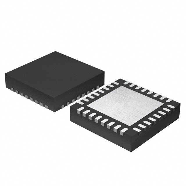
32-lead, 5 mm × 5 mm LFCSP_CAV package
Point to point radios
Point to multipoint radios
Microwave radios, very small aperture terminals (VSATs),
and satellite communications (SATCOM)
Military and space
1
2
3
4
5
6
7
8
2kΩ
2kΩ
24
23
22
21
20
19
18
17
GND
NIC
GND
RFOUT
GND
VDET
VREF
GND
PACKAGE
BASE
GND
16864-001
APPLICATIONS
GND
NIC
GND
RFIN
GND
NIC
NIC
GND
GND 9
VG2 10
VD2 11
VD4 12
VD6 13
NIC 14
VD8 15
GND 16
Data Sheet
>1.5 W (34 dBm), 24 GHz to 34 GHz,
GaAs, pHEMT, MMIC, Power Amplifier
HMC943APM5E
Figure 1.
GENERAL DESCRIPTION
The HMC943APM5E is a four stage, gallium arsenide (GaAs),
pseudomorphic high electron mobility transistor (pHEMT),
monolithic microwave integrated circuit (MMIC), >1.5 W
power amplifier that operates between 24 GHz to 34 GHz. The
HMC943APM5E provides 23 dB of gain, 34 dBm of saturated
output power (PSAT), and 23% power added efficiency (PAE)
from a 5.5 V supply. The high output third-order intercept (IP3)
Rev. B
of 39 dBm makes the HMC943APM5E ideal for microwave
radio applications. A power detector output is also available.
The HMC943APM5E amplifier input/outputs (I/Os) are
internally matched to 50 Ω. The device is packaged in a leadless,
5 mm × 5 mm, surface-mount LFCSP_CAV package, and
requires no external matching components.
Document Feedback
Information furnished by Analog Devices is believed to be accurate and reliable. However, no
responsibility is assumed by Analog Devices for its use, nor for any infringements of patents or other
rights of third parties that may result from its use. Specifications subject to change without notice. No
license is granted by implication or otherwise under any patent or patent rights of Analog Devices.
Trademarks and registered trademarks are the property of their respective owners.
One Technology Way, P.O. Box 9106, Norwood, MA 02062-9106, U.S.A.
Tel: 781.329.4700
©2018 Analog Devices, Inc. All rights reserved.
Technical Support
www.analog.com
�HMC943APM5E
Data Sheet
TABLE OF CONTENTS
Features .............................................................................................. 1
Pin Configuration and Function Descriptions..............................5
Applications ....................................................................................... 1
Interface Schematics .....................................................................6
Functional Block Diagram .............................................................. 1
Typical Performance Characteristics ..............................................7
General Description ......................................................................... 1
Theory of Operation ...................................................................... 14
Revision History ............................................................................... 2
Applications Information .............................................................. 15
Specifications..................................................................................... 3
Power Detection ......................................................................... 15
Electrical Specifications ............................................................... 3
Evaluation Board ............................................................................ 16
Absolute Maximum Ratings............................................................ 4
Evaluation Board Schematic ..................................................... 17
Thermal Resistance ...................................................................... 4
Outline Dimensions ....................................................................... 18
ESD Caution .................................................................................. 4
Ordering Guide .......................................................................... 18
REVISION HISTORY
11/2018—Rev. A to Rev. B
Changes to Figure 1 .......................................................................... 1
Changes to Table 5 ............................................................................ 5
Changes to Figure 4 and Figure 6 ................................................... 6
Changes to Figure 51 ...................................................................... 17
9/2018—Rev. 0 to Rev. A
Changes to Storage Temperature Range Parameter, Table 3 ....... 4
8/2018—Revision 0: Initial Version
Rev. B | Page 2 of 18
�Data Sheet
HMC943APM5E
SPECIFICATIONS
ELECTRICAL SPECIFICATIONS
TA = 25°C, VD1 − VD8 = 5.5 V, quiescent supply current (IDDQ) = 1300 mA, and frequency range = 24 GHz to 29 GHz
Table 1.
Parameter
FREQUENCY RANGE
GAIN
Gain Variation over
Temperature
RETURN LOSS
Input
Output
POWER
Output Power for 1 dB
Compression
Saturated Output Power
Symbol
23
0.04
Unit
GHz
dB
dB/°C
12
12
dB
dB
33
dBm
PSAT
34
dBm
OUTPUT THIRD-ORDER
INTERCEPT
SUPPLY VOLTAGE
QUIESCENT SUPPLY
CURRENT
IP3
39
dBm
P1dB
VDD
IDDQ
Min
24
20.5
29
4
Typ
5.5
1300
Max
29
6
V
mA
Test Conditions/Comments
Output power (POUT) per tone = 22 dBm
Adjust VG1 or VG2 between −2 V and 0 V to achieve 1300 mA typical,
VGx = −0.85 V typical to achieve IDDQ = 1300 mA
TA = 25°C, VD1 − VD8 = 5.5 V, IDDQ = 1300 mA, and frequency range = 29 GHz to 34 GHz
Table 2.
Parameter
FREQUENCY RANGE
GAIN
Gain Variation over
Temperature
RETURN LOSS
Input
Output
POWER
Output Power for 1 dB
Compression
Saturated Output Power
OUTPUT THIRD-ORDER
INTERCEPT
SUPPLY VOLTAGE
QUIESCENT SUPPLY
CURRENT
Symbol
P1dB
Min
29
20.5
30
PSAT
IP3
VDD
IDDQ
4
Typ
23
0.04
Unit
GHz
dB
dB/°C
10
13
dB
dB
33
dBm
34
37.5
dBm
dBm
5.5
1300
Max
34
6
V
mA
Test Conditions/Comments
POUT per tone = 22 dBm
Adjust VG1 or VG2 between −2 and 0 V to achieve 1300 mA typical,
VGx = −0.85 V typical to achieve IDDQ = 1300 mA
Rev. B | Page 3 of 18
�HMC943APM5E
Data Sheet
ABSOLUTE MAXIMUM RATINGS
THERMAL RESISTANCE
Table 3.
Parameter
Drain Bias Voltage (VDx)
Gate Bias Voltage (VGx)
Radio Frequency (RF) Input Power (RFIN)
Output Load Standing Wave Ratio (VSWR)
Junction Temperature to Maintain 1 Million
Hour Mean Time to Failure (MTTF)
Maximum Peak Reflow Temperature (MSL3)2
Nominal Junction Temperature
(TA = 85°C, VDx = 5.5 V)
Continuous Power Dissipation, PDISS (TA =
85°C, Derate 116.3 m W/°C Above 85°C)
Storage Temperature Range
Operating Temperature Range
ESD Sensitivity (Human Body Model)
1
Rating
6.5 V
−2 V to 0 V dc
20 dBm
7:1
175°C
Thermal performance is directly linked to printed circuit board
(PCB) design and operating environment. Careful attention to
PCB thermal design is required.
θJC is the junction to case thermal resistance.
Table 4. Thermal Resistance
Package Type
CG-32-21
260°C
146.5°C
1
10.5 W
−65°C to +150°C
−40°C to +85°C
Class 0B, passed
150 V
θJC
8.6
Unit
°C/W
Thermal resistance (θJC) is determined by simulation under the following
conditions: the heat transfer is due solely to thermal conduction from the
channel, through the ground pad, to the PCB, and the ground pad is held
constant at the operating temperature of 85°C.
ESD CAUTION
When referring to a single function of a multifunction pin in the parameters,
only the portion of the pin name that is relevant to the Absolute Maximum
Rating is listed. For full pin names of multifunction pins, refer to the Pin
Configuration and Function Descriptions section.
2
See the Ordering Guide for additional information.
1
Stresses at or above those listed under Absolute Maximum
Ratings may cause permanent damage to the product. This is a
stress rating only; functional operation of the product at these
or any other conditions above those indicated in the operational
section of this specification is not implied. Operation beyond
the maximum operating conditions for extended periods may
affect product reliability.
Rev. B | Page 4 of 18
�Data Sheet
HMC943APM5E
32
31
30
29
28
27
26
25
GND
VG1
VD1
VD3
VD5
NIC
VD7
GND
PIN CONFIGURATION AND FUNCTION DESCRIPTIONS
1
2
3
4
5
6
7
8
HMC943APM5E
TOP VIEW
(Not to Scale)
24
23
22
21
20
19
18
17
GND
NIC
GND
RFOUT
GND
VDET
VREF
GND
NOTES
1. NIC = NOT INTERNALLY CONNECTED.
2. THE EXPOSED PAD MUST BE CONNECTED
TO RF AND DC GROUND.
16864-002
GND 9
VG2 10
VD2 11
VD4 12
VD6 13
NIC 14
VD8 15
GND 16
GND
NIC
GND
RFIN
GND
NIC
NIC
GND
Figure 2. Pin Configuration
Table 5. Pin Function Descriptions
Pin No.
1, 3, 5, 8, 9,
16, 17, 20,
22, 24, 25,
32
2, 6, 7, 14,
23, 27
4
10, 31
Mnemonic
GND
Description
Ground. These pins are exposed ground pads that must be connected to RF and dc ground.
NIC
11, 12, 13,
15, 26, 28,
29, 30
18
VD2, VD4, VD6, VD8,
VD7, VD5, VD3, and
VD1
VREF
Not Internally Connected. These pins are not connected internally. However, all data is measured with
these pins connected to RF and dc ground externally.
RF Input. This pin is dc-coupled and matched to 50 Ω. See Figure 4 for the RFIN interface schematic.
Gate Control for the Amplifier. Adjust VGx to achieve the recommended bias current. External bypass
capacitors of 100 pF, 10 nF, and 4.7 μF are required. See Figure 7 for the VGx interface schematic. VG1 and
VG2 are internally connected. Therefore, external bias can be applied to either VG1 or VG2.
Drain Bias for the Amplifier. External bypass capacitors of 100 pF, 0.01 µF, and 4.7 µF are required on each
pin. See Figure 5 for the VDx interface schematic.
19
VDET
21
RFOUT
RFIN
VG2, VG1
EPAD
Reference Diode Used for Temperature Compensation of VDET RF Output Power Measurements. Used in
combination with VDET, this voltage provides temperature compensation to VDET RF output power
measurements. See Figure 8 for the VREF interface schematic.
Detector Diode Used for Measurement of the RF Output Power. Detection via this pin requires the
application of a dc bias voltage through the external series resistor. Used in combination with VREF, the
difference voltage, VREF − VDET, is a temperature compensated dc voltage proportional to the RF output
power. See Figure 9 for the VDET interface schematic.
RF Signal Output. This pad is dc-coupled and matched to 50 Ω over the operating frequency range. See
Figure 6 for the RFOUT interface schematic.
Exposed Pad. The exposed pad must be connected to RF and dc ground.
Rev. B | Page 5 of 18
�HMC943APM5E
Data Sheet
INTERFACE SCHEMATICS
RFOUT
16864-003
2.0kΩ
Figure 3. GND Interface Schematic
16864-006
GND
Figure 6. RFOUT Interface Schematic
Figure 4. RFIN Interface Schematic
VG1, VG2
16864-007
2.0kΩ
16864-004
RFIN
Figure 7. VG1, VG2 Interface Schematic
VREF
16864-008
16864-005
VD1 TO VD8
Figure 5. VD1 to VD8 Interface Schematic
VDET
16864-009
Figure 8. VREF Interface Schematic
Figure 9. VDET Interface Schematic
Rev. B | Page 6 of 18
�Data Sheet
HMC943APM5E
30
30
25
28
20
26
15
24
5
GAIN (dB)
INPUT RETURN LOSS
BROADBAND GAIN
OUTPUT RETURN LOSS
0
22
20
18
–5
16
–10
14
–15
12
–20
20
24
22
26
28
30
32
34
36
38
FREQUENCY (GHz)
10
23
25
26
28
27
29
30
31
32
33
34
Figure 13. Gain vs. Frequency at Various Temperatures
0
0
–5
–5
S22 (dB)
–10
+85°C
+25°C
–40°C
–10
24
25
26
27
28
29
30
31
32
33
34
FREQUENCY (GHz)
–20
23
16864-011
–20
23
+85°C
+25°C
–40°C
Figure 11. Input Return Loss (S11) vs. Frequency at Various Temperatures
36
34
34
32
32
P1dB (dBm)
36
24
24
+85°C
+25°C
–40°C
25
26
27
28
29
30
31
32
33
34
FREQUENCY (GHz)
35
29
30
31
32
33
34
4.0V
4.5V
5.0V
5.5V
6.0V
22
16864-012
24
28
28
26
20
23
27
30
26
22
26
Figure 14. Output Return Loss (S22) vs. Frequency at Various Temperatures
38
28
25
FREQUENCY (GHz)
38
30
24
16864-014
–15
–15
Figure 12. P1dB vs. Frequency at Various Temperatures
20
23
24
25
26
27
28
29
30
31
32
33
34
FREQUENCY (GHz)
Figure 15. P1dB vs. Frequency at Various Supply Voltages
Rev. B | Page 7 of 18
35
16864-015
S11 (dB)
24
FREQUENCY (GHz)
Figure 10. Broadband Gain (S21), Input Return Loss (S11), and
Output Return Loss (S22) Response vs. Frequency
P1dB (dBm)
+85°C
+25°C
–40°C
16864-013
10
16864-010
RESPONSE (dB)
TYPICAL PERFORMANCE CHARACTERISTICS
�Data Sheet
38
38
36
36
34
34
32
32
PSAT (dBm)
30
28
26
28
26
24
1400mA
1300mA
1200mA
1000mA
24
25
26
27
28
29
30
31
32
33
34
35
FREQUENCY (GHz)
20
23
36
36
34
34
32
32
PSAT (dBm)
26
27
28
29
30
31
32
33
34
35
30
28
30
28
26
4.0V
4.5V
5.0V
5.5V
6.0V
22
24
25
24
1400mA
1300mA
1200mA
1000mA
22
26
27
28
29
30
31
32
33
34
35
FREQUENCY (GHz)
20
23
16864-017
24
24
25
26
27
28
29
30
31
32
33
34
35
FREQUENCY (GHz)
Figure 17. PSAT vs. Frequency at Various Supply Voltages
16864-020
PSAT (dBm)
38
26
Figure 20. PSAT vs. Frequency at Various Quiescent Currents
50
50
+85°C
+25°C
–40°C
45
45
OUTPUT IP3 (dBm)
40
35
30
25
20
40
35
30
25
4.0V
4.5V
5.0V
5.5V
6.0V
20
24
25
26
27
28
29
30
31
32
33
34
35
FREQUENCY (GHz)
16864-018
OUTPUT IP3 (dBm)
25
Figure 19. PSAT vs. Frequency at Various Temperatures
38
15
23
24
FREQUENCY (GHz)
Figure 16. P1dB vs. Frequency at Various Quiescent Currents
20
23
+85°C
+25°C
–40°C
22
16864-016
22
16864-019
24
20
23
30
Figure 18. Output IP3 vs. Frequency at Various Temperatures,
POUT per Tone = 22 dBm
15
23
24
25
26
27
28
29
30
31
32
33
34
35
FREQUENCY (GHz)
Figure 21. Output IP3 vs. Frequency at Various Supply Voltages,
POUT per Tone = 22 dBm
Rev. B | Page 8 of 18
16864-021
P1dB (dBm)
HMC943APM5E
�Data Sheet
HMC943APM5E
45
50
34GHz
32GHz
30GHz
28GHz
26GHz
24GHz
40
45
OUTPUT IM3 (dBc)
35
30
25
26
15
5
27
28
29
31
30
32
34
33
35
FREQUENCY (GHz)
0
18
22
23
24
25
26
26
26
50
34GHz
32GHz
30GHz
28GHz
26GHz
24GHz
45
40
40
OUTPUT IM3 (dBc)
35
30
25
20
15
35
30
25
20
15
10
10
5
5
19
20
21
22
23
24
25
34GHz
32GHz
30GHz
28GHz
26GHz
24GHz
45
26
POUT/TONE (dBm)
0
18
16864-023
OUTPUT IM3 (dBc)
21
Figure 25. Output IM3 vs. POUT per Tone, VDD = 4.0 V
50
19
20
21
22
23
24
25
POUT/TONE (dBm)
Figure 23. Output Third-Order Intermodulation Distortion (IM3)
vs. POUT per Tone, VDD = 4.5 V
Figure 26. Output IM3 vs. POUT per Tone, VDD = 5.0 V
50
50
34GHz
32GHz
30GHz
28GHz
26GHz
24GHz
45
40
40
OUTPUT IM3 (dBc)
35
34GHz
32GHz
30GHz
28GHz
26GHz
24GHz
45
30
25
20
15
10
35
30
25
20
15
10
5
5
0
18
0
18
19
20
21
22
23
24
25
POUT/TONE (dBm)
26
16864-024
OUTPUT IM3 (dBc)
20
POUT/TONE (dBm)
Figure 22. Output IP3 vs. Frequency at Various Quiescent Currents,
POUT per Tone = 22 dBm
0
18
19
16864-025
25
20
16864-026
24
25
16864-027
15
23
30
10
1400mA
1300mA
1200mA
1000mA
20
16864-022
OUTPUT IP3 (dBm)
35
40
Figure 24. Output IM3 vs. POUT per Tone, VDD = 5.5 V
19
20
21
22
23
24
25
POUT/TONE (dBm)
Figure 27. Output IM3 vs. POUT per Tone, VDD = 6.0 V
Rev. B | Page 9 of 18
�HMC943APM5E
Data Sheet
45
40
–40°C
+25°C
+85°C
40
35
30
25
25
PAE (%)
20
20
15
15
10
10
27
28
29
30
31
32
33
34
35
FREQUENCY (GHz)
0
32
GAIN (dB), POUT (dBm), PAE (%)
30
PAE (%)
25
20
15
10
5
23
24
25
26
27
28
29
30
31
33
32
34
35
FREQUENCY (GHz)
28
1400
12
1300
8
1200
4
0
–15
–10
–5
0
5
10
15
GAIN (dB), POUT (dBm), PAE (%)
1700
16
34
35
1900
POUT
GAIN
PAE
I DD
1800
1700
1400
12
1300
8
1200
4
1100
32
1500
33
16
1800
20
32
1500
36
1600
31
30
20
1900
24
29
–10
–5
0
5
10
15
1000
INPUT POWER (dBm)
28
2100
POUT
GAIN
PAE
I DD
2000
1900
24
1800
20
1700
16
1600
12
1500
8
1400
1100
4
1300
1000
0
–15
INPUT POWER (dBm)
IDD (mA)
28
28
Figure 32. Gain, POUT, PAE, and IDD vs. Input Power,
Power Compression at 24 GHz
16864-031
GAIN (dB), POUT (dBm), PAE (%)
32
POUT
GAIN
PAE
I DD
27
1600
Figure 29. PAE vs. Frequency at Various Supply Voltages, PAE Measured
at PSAT
36
26
24
0
–15
16864-129
0
25
Figure 31. PAE vs. Frequency at Various Quiescent Currents, PAE Measured
at PSAT
36
4V
4.5V
5V
5.5V
6V
35
24
FREQUENCY (GHz)
Figure 28. PAE vs. Frequency at Various Temperatures, PAE Measured at PSAT
40
23
IDD (mA)
26
16864-028
25
Figure 30. Gain, POUT, PAE, and Drain Current (IDD) vs. Input Power,
Power Compression at 29 GHz
–10
–5
0
5
10
INPUT POWER (dBm)
Figure 33. Gain, POUT, PAE, and IDD vs. Input Power,
Power Compression at 34 GHz
Rev. B | Page 10 of 18
15
1200
IDD (mA)
24
16864-128
23
16864-131
5
5
16864-029
PAE (%)
30
0
1000mA
1200mA
1300mA
1400mA
35
�HMC943APM5E
37
35
35
33
31
29
27
25
23
GAIN
P1dB
P SAT
17
4.0
4.5
5.0
5.5
29
27
25
23
21
6.0
VDD (V)
17
4.0
GAIN (dB), P1dB (dBm), PSAT (dBm)
35
33
31
29
27
25
23
GAIN
P1dB
P SAT
4.5
5.0
5.5
6.0
VDD (V)
31
29
27
25
23
21
17
600
GAIN (dB), P1dB (dBm), PSAT (dBm)
35
33
31
29
27
25
23
GAIN
P1dB
P SAT
800
900
1000
1100
1200
1300
IDDQ (mA)
800
900
1000
1100
1200
1300
1400
1400
33
31
29
27
25
23
21
GAIN
P1dB
PSAT
19
1400
16864-035
GAIN (dB), P1dB (dBm), PSAT (dBm)
37
700
700
Figure 38. Gain, P1dB, and PSAT vs. IDDQ at 24 GHz
37
17
600
GAIN
P1dB
PSAT
IDDQ (mA)
35
19
6.0
33
Figure 35. Gain, P1dB, and PSAT vs. VDD at 34 GHz
21
5.5
19
16864-034
GAIN (dB), P1dB (dBm), PSAT (dBm)
37
35
17
4.0
5.0
Figure 37. Gain, P1dB, and PSAT vs. VDD at 29 GHz
37
19
4.5
VDD (V)
Figure 34. Gain, P1dB, and PSAT vs. VDD at 24 GHz
21
GAIN
P1dB
P SAT
19
16864-037
19
31
16864-038
21
33
16864-033
GAIN (dB), P1dB (dBm), PSAT (dBm)
37
16864-030
GAIN (dB), P1dB (dBm), PSAT (dBm)
Data Sheet
17
600
700
800
900
1000
1100
1200
1300
IDDQ (mA)
Figure 39. Gain, P1dB, and PSAT vs. IDDQ at 34 GHz
Figure 36. Gain, P1dB, and PSAT vs. IDDQ at 29 GHz
Rev. B | Page 11 of 18
�HMC943APM5E
Data Sheet
10
0
34GHz
29GHz
24GHz
+85°C
+25°C
–40°C
–10
VREF – VDET (V)
S12 (dB)
–20
–30
–40
1
–50
24
26
28
30
32
34
36
FREQUENCY (GHz)
0.1
16864-032
–70
22
5
20
25
30
35
40
Figure 43. VREF – VDET vs. Output Power at Various Frequencies
10
10
+85°C
+25°C
–40°C
1
5
10
15
20
25
30
35
40
OUTPUT POWER (dBm)
Figure 41. VREF – VDET vs. Output Power at Various Temperatures at 24 GHz
1
0.1
5
10
15
20
25
30
35
40
OUTPUT POWER (dBm)
16864-040
VREF – VDET (V)
+85°C
+25°C
–40°C
16864-039
VREF – VDET (V)
15
OUTPUT POWER (dBm)
Figure 40. Reverse Isolation (S12) vs. Frequency at Various Temperatures
0.1
10
16864-036
–60
Figure 44. VREF – VDET vs. Output Power at Various Temperatures at 29 GHz
10
5
+85°C
+25°C
–40°C
0
–10
1
–15
–20
34GHz
31GHz
30GHz
29GHz
28GHz
27GHz
26GHz
24GHz
–25
0.1
5
11
17
23
OUTPUT POWER (dBm)
29
35
16864-043
–30
Figure 42. VREF – VDET vs. Output Power at Various Temperatures at 34 GHz
Rev. B | Page 12 of 18
–35
0
2.5
5.0
7.5
10.0
12.5
15.0
INPUT POWER (dBm)
Figure 45. Gate Current (IGG) vs. Input Power at Various Frequencies
16864-041
IGG (mA)
VREF – VDET (V)
–5
�Data Sheet
HMC943APM5E
12
1700
1500
1300
1100
24GHz
26GHz
27GHz
28GHz
29GHz
30GHz
31GHz
34GHz
MAXIMUM PDISS AT 85ºC
4
2
0
0
1
2
3
4
5
6
7
900
700
500
300
100
8
9
10 11 12 13 14 15
INPUT POWER (dBm)
–100
–2.0
Figure 46. Power Dissipation vs. Input Power at Various Frequencies,
TA = 85°C
–1.8
–1.6
–1.4
VG (V)
–1.2
–1.0
–0.8
16864-042
6
IDDQ (mA)
8
16864-044
POWER DISSIPATION (W)
10
Figure 47. IDDQ vs. Gate Bias Voltage (VGx), VDx = 5.5 V, Representative of a
Typical Device
Rev. B | Page 13 of 18
�HMC943APM5E
Data Sheet
THEORY OF OPERATION
Device drain connections for all stages are available at the package
leads. Gate voltage bias can be applied to either VG1 or VG2
because the bias is internally connected to the gates of devices
for all stages.
The HMC943APM5E is a GaAs, pHEMT, MMIC, >1.5 W power
amplifier consisting of four cascaded gain stages. A simplified
schematic is shown in Figure 48. The input signal is evenly divided
and amplified through four gain stages. These amplified signals
are then recombined at the output. Both inputs and outputs are
internally matched to 50 Ω for ease of use.
VG1
VD1
VD3
VD5
VD7
VD2
VD4
VD6
VD8
VG2
Figure 48. Simplified Schematic Diagram of Amplifier Stages
Rev. B | Page 14 of 18
16864-045
RFOUT
RFIN
�Data Sheet
HMC943APM5E
APPLICATIONS INFORMATION
The HMC943A is a GaAs, pHEMT, MMIC power amplifier.
Capacitive bypassing is required for VDx as well as for VGx (see
Figure 51). Drain bias voltage must be applied to all VDx pins,
and gate bias voltage must be applied to VGx. Though the RFIN
and RFOUT ports ac couple the signal, dc paths to GND are provided
to increase the ESD robustness of the device. External dc blocking
of both RFIN and RFOUT is desirable when appreciable levels of dc
are expected to be present.
The bias conditions previously listed (VDx = 5.5 V, IDDQ = 1300 mA)
are the recommended operating points to achieve optimum
performance. The data used in this data sheet is taken with the
recommended bias conditions. When using the HMC943APM5E
with different bias conditions, different performance conclusions
may result other than from what is shown in the Typical
Performance Characteristics section.
The VDET and VREF pins are the output pins for the internal power
detector. The VDET pin is the dc voltage output pin that represents
the RF output power rectified by the internal diode and capacitor,
which is biased through an external resistor. The VREF pin is the dc
voltage output pin that represents the reference diode voltage,
which is biased through an external resistor. This voltage is then
used to compensate for the temperature variation effects on both
diodes. A typical circuit is shown in the Evaluation Board
Schematic section that reads out the output voltage and
represents the RF output power as shown in Figure 51.
All measurements for this device are taken using the evaluation
board schematic shown in Figure 51, configured as shown in the
evaluation PCB in Figure 50.
The recommended bias sequence during power-up is as follows:
5.
Connect the power supply ground to circuit ground (GND).
Set VG1 or VG2 to −2 V.
Set VDx to 5.5 V.
Slowly increase VG1 or VG2 from −2 V until typical
IDDQ = 1300 mA is reached.
Apply the RF signal.
POWER DETECTION
This device has internal output power detection, shown in
Figure 49. Power detection is achieved through referencing
VREF – VDET to the corresponding output power. The sensing
circuit is composed of two diode connected circuit paths, VREF
and VDET. VDET changes when the RF output signal couples to
the VDET path. The coupled RF signal is then rectified by the
detector diode and smoothed out by the shunt capacitor. Because
the forward bias voltage for the detector diode is temperature
dependent, VREF is used as reference to compensate for temperature
in calculation.
The recommended bias sequence during power-down is as
follows:
1.
2.
3.
4.
Turn the RF signal off.
Decrease VG1 or VG2 back to −2 V.
Decrease VDx to 0 V.
Decrease VG1 or VG2 to 0 V.
RFIN
RFOUT
EXTERNAL CIRCUIT
40kΩ
VDET
VREF
+6V
40kΩ
Figure 49. Power Detection Circuit
Rev. B | Page 15 of 18
16864-046
1.
2.
3.
4.
�HMC943APM5E
Data Sheet
EVALUATION BOARD
The HMC943APM5E evaluation board is a 2-layer board
fabricated using Rogers 4350 material and best practices for
high frequency RF design. The RF input and RF output traces
have a 50 Ω characteristic impedance. The circuit board is
attached to a heat sink using SN96 solder and provides a low
thermal resistance path. Components are mounted using SN63
solder, allowing rework of the surface-mount components
without compromising the circuit board to heat sink attachment.
The evaluation board schematic is shown in Figure 51. A fully
populated and tested evaluation board (see Figure 50) is available
from Analog Devices, Inc., upon request.
Table 6. Bill of Materials for Evaluation PCB EV1HMC943APM5
Item
J7, J2
J3, J4
C1 to C10
C11 to C20
C21 to C30
R1, R2
U1
Heat Sink
PCB
1
Description
Connectors, SRI K connector, SRI 25-146-1000-92
DC pins
100 pF capacitors, 0402 package
10,000 pF capacitors, 0402 package
4.7 μF capacitors, Case A package
40.2 kΩ resistors, 0402 package
HMC943APM5E amplifier
Used for thermal transfer from the HMC943APM5E amplifier
EV1HMC943APM51
Circuit board material is Rogers 4350.
Rev. B | Page 16 of 18
16864-047
The evaluation board and populated components are designed
to operate over the ambient temperature range of −40°C to
+85°C. During operation, to control the temperature of the
HMC943APM5E, attach the evaluation board to a temperature
controlled plate. For proper bias sequence, see the Applications
Information section.
Figure 50. Evaluation PCB
�Data Sheet
HMC943APM5E
EVALUATION BOARD SCHEMATIC
VD3
P+ C28
N 4.7µF
GND
C18
0.01µF
C8
100pF
GND
GND
VD1
VD5
P+ C29
N 4.7µF
GND
C19
0.01µF
C9
100pF
GND
GND
C7
100pF
C17
0.01µF
C27
4.7µF
GND
GND
GND
VG1
N
P+
+P
N
VD7
VD5
VD3
VD1
VG1
VD7
C30
4.7µF
C20
0.01µF
C10
100pF
GND
GND
GND
C6
100pF
C16
0.01µF
C26
4.7µF
GND
GND
GND
+P
J3
J3
2
4
6
8
10
1
3
5
7
9
J4
J4
N
GND
PAD
32
31
30
29
28
27
26
25
HMC943APM5E
234
GND
2kΩ
24
23
22
21
20
19
18
17
J2
RFOUT
R2
VDET
40.2kΩ
VREF
GND
R1
VDD6
1
25-146-1000-92
4 3 2
GND
40.2kΩ
GND
VG2
N
P+
VG2
VD2
VD4
VD6
VD8
VREF
VDD6
VD8
C21
4.7µF
C11
0.01µF
C1
100pF
GND
GND
GND
C5
100pF
C15
0.01µF
C25
4.7µF
GND
GND
GND
VD2
P+ C22
4.7µF
N
GND
+P
N
2
4
6
8
10
12
14
1
3
5
7
9
11
13
87759-1450
VDET
GND
VD6
C12
0.01µF
C2
100pF
GND
GND
C13
0.01µF
C3
100pF
GND
GND
C4
100pF
C14
0.01µF
C24
4.7µF
GND
GND
GND
+P
N
VD4
P+ C23
4.7µF
N
GND
DNI
25-146-1000-92
1
J5
2 3 4
GND
Figure 51. Evaluation Board Schematic
Rev. B | Page 17 of 18
THRUCAL
J6
1
DNI
25-146-1000-92
432
GND
16864-048
1
1
2
3
4
5
6 2kΩ
7
8
RFIN
9
10
11
12
13
14
15
16
25-146-1000-92
J7
�HMC943APM5E
Data Sheet
OUTLINE DIMENSIONS
DETAIL A
(JEDEC 95)
5.10
5.00 SQ
4.90
25
3.20
3.10 SQ
3.00
EXPOSED
PAD
17
0.45
0.40
0.35
PKG-005068
1.35
1.25
1.15
0.60 REF SIDE VIEW
8
9
16
BOTTOM VIEW
0.40
0.050 MAX
0.035 NOM
COPLANARITY
0.08
0.203 REF
SEATING
PLANE
(SEE DETAIL A)
1
0.50
BSC
TOP VIEW
PIN 1
INDICATOR AREA OPTIONS
32
24
3.50 REF
FOR PROPER CONNECTION OF
THE EXPOSED PAD, REFER TO
THE PIN CONFIGURATION AND
FUNCTION DESCRIPTIONS
SECTION OF THIS DATA SHEET.
08-15-2018-A
PIN 1
INDICATOR
0.30
0.25
0.20
Figure 52. 32-Lead Lead Frame Chip Scale Package [LFCSP_CAV]
5 mm × 5 mm Body and 1.25 mm Package Height
(CG-32-2)
Dimensions shown in millimeters
ORDERING GUIDE
Model1, 2
HMC943APM5E
HMC943APM5ETR
EV1HMC943APM5
Temperature Range
−40°C to +85°C
−40°C to +85°C
Moisture Sensitivity Level (MSL) Rating3
MSL3
MSL3
1
All models are RoHS compliant parts.
When ordering the evaluation board, reference Model Number EV1HMC943APM5.
See the Absolute Maximum Ratings section for additional information.
4
The lead finish of the HMC943APM5E and the HMC943APM5ETR is nickel palladium gold (NiPdAu).
2
3
©2018 Analog Devices, Inc. All rights reserved. Trademarks and
registered trademarks are the property of their respective owners.
D16864-0-11/18(B)
Rev. B | Page 18 of 18
Package Description4
32-Lead LFCSP_CAV
32-Lead LFCSP_CAV
Evaluation Board
Package Option
CG-32-2
CG-32-2
�


 工商网监
湘ICP备2023018690号
工商网监
湘ICP备2023018690号
