IA186EM/IA188EM
8-Bit/16-Bit Microcontrollers
Data Sheet
February 25, 2011
®
IA186EM/IA188EM
8-Bit/16-Bit Microcontrollers
Data Sheet
®
IA211050831-19
UNCONTROLLED WHEN PRINTED OR COPIED
Page 1 of 146
http://www.Innovasic.com
Customer Support:
1-888-824-4184
�IA186EM/IA188EM
8-Bit/16-Bit Microcontrollers
Copyright
Data Sheet
February 25, 2011
2011 by Innovasic Semiconductor, Inc.
Published by Innovasic Semiconductor, Inc.
3737 Princeton Drive NE, Suite 130, Albuquerque, NM 87107
AMD, Am186, and Am188 are trademarks of Advanced Micro Devices, Inc.
MILES™ is a trademark of Innovasic Semiconductor, Inc.
®
IA211050831-19
UNCONTROLLED WHEN PRINTED OR COPIED
Page 2 of 146
http://www.Innovasic.com
Customer Support:
1-888-824-4184
�IA186EM/IA188EM
8-Bit/16-Bit Microcontrollers
Data Sheet
February 25, 2011
TABLE OF CONTENTS
List of Figures ..................................................................................................................................8
List of Tables ...................................................................................................................................9
Conventions ...................................................................................................................................12
Acronyms and Abbreviations ........................................................................................................13
1.
Introduction...........................................................................................................................14
1.1 General Description.....................................................................................................14
1.2 Features .......................................................................................................................14
2.
Packaging , Pin Descriptions, and Physical Dimensions ......................................................15
2.1 Packages and Pinouts ..................................................................................................15
2.1.1 IA186EM TQFP Package ...............................................................................16
2.1.2 IA188EM TQFP Package ...............................................................................19
2.1.3 TQFP Physical Dimensions ............................................................................22
2.1.4 IA186EM PQFP Package ...............................................................................23
2.1.5 IA188EM PQFP Package ...............................................................................26
2.1.6 PQFP Physical Dimensions ............................................................................29
2.2 Pin Descriptions ..........................................................................................................30
2.2.1 a19/pio9, a18/pio8, a17/pio7, a16–a0—Address Bus (synchronous
outputs with tristate) .......................................................................................30
2.2.2 ad15–ad8 (IA186EM)—Address/data bus (level-sensitive
synchronous inouts with tristate) ....................................................................30
2.2.3 ad7–ad0—Address/Data bus (level-sensitive synchronous inouts with
tristate) ............................................................................................................30
2.2.4 ao15–ao8 (IA188EM)—Address-only bus (level-sensitive
synchronous outputs with tristate) ..................................................................30
2.2.5 ale—Address Latch Enable (synchronous output) .........................................31
2.2.6 ardy—Asynchronous Ready (level-sensitive asynchronous input) ................31
2.2.7 bhe_n/aden_n (IA186EM)—Bus High Enable (synchronous output
with tristate)/Address Enable (input with internal pull-up) ............................31
2.2.8 clkouta—Clock Output A (synchronous output) ............................................32
2.2.9 clkoutb—Clock Output B (synchronous output) ............................................32
2.2.10 den_n/pio5—Data Enable Strobe (synchronous output with tristate) ............32
2.2.11 drq1/pio12–drq0/pio13—DMA Requests (synchronous level-sensitive
inputs) .............................................................................................................32
2.2.12 dt/r_n/pio4—Data Transmit or Receive (synchronous output with
tristate) ............................................................................................................32
2.2.13 gnd—Ground ..................................................................................................32
2.2.14 hlda—Bus Hold Acknowledge (synchronous output) ....................................33
2.2.15 hold—Bus Hold Request (synchronous level-sensitive input) .......................33
2.2.16 int0—Maskable Interrupt Request 0 (asynchronous input) ............................33
2.2.17 int1/select_n—Maskable Interrupt Request 1/Slave Select (both are
asynchronous inputs) ......................................................................................33
®
IA211050831-19
UNCONTROLLED WHEN PRINTED OR COPIED
Page 3 of 146
http://www.Innovasic.com
Customer Support:
1-888-824-4184
�IA186EM/IA188EM
8-Bit/16-Bit Microcontrollers
Data Sheet
February 25, 2011
2.2.18 int2/inta0_n/pio31—Maskable Interrupt Request 2 (asynchronous
input)/Interrupt Acknowledge 0 (synchronous output) ..................................34
2.2.19 int3/inta1_n/irq—Maskable Interrupt Request 3 (asynchronous
input)/Interrupt Acknowledge 1 (synchronous output)/Interrupt
Acknowledge (synchronous output) ...............................................................34
2.2.20 int4/pio30—Maskable Interrupt Request 4 (asynchronous input)..................34
2.2.21 lcs_n/once0_n—Lower Memory Chip Select (synchronous output
with internal pull-up)/ONCE Mode Request (input) ......................................35
2.2.22 mcs2_n—mcs0_n (no pio, pio15, pio 14)—Midrange Memory Chip
Selects (synchronous outputs with internal pull-up) ......................................35
2.2.23 mcs3_n/rfsh_n (pio25)—Midrange Memory Chip Select
(synchronous output with internal pull-up)/Automatic Refresh
(synchronous output) ......................................................................................35
2.2.24 nmi—Nonmaskable Interrupt (synchronous edge-sensitive input) ................35
2.2.25 pcs3_n–pcs0_n (pio19–pio16)—Peripheral Chip Selects 3–0
(synchronous outputs) .....................................................................................36
2.2.26 pcs5_n/a1—Peripheral Chip Select 5 (synchronous output)/Latched
Address Bit 1 (synchronous output) ...............................................................36
2.2.27 pcs6_n/a2—Peripheral Chip Select 6 (synchronous output)/latched
Address Bit 2 (synchronous output) ...............................................................36
2.2.28 pio31–pio0—Programmable I/O Pins (asynchronous input/output
open-drain) ......................................................................................................37
2.2.29 rd_n—Read strobe (synchronous output with tristate) ...................................37
2.2.30 res_n—Reset (asynchronous level-sensitive input) ........................................37
2.2.31 rfsh2_n/aden_n (IA188EM)—Refresh 2 (synchronous output with
tristate)/Address Enable (input with internal pull-up) ....................................37
2.2.32 rxd/pio28—Receive Data (asynchronous input) ............................................37
2.2.33 s2_n–s0_n—Bus Cycle Status (synchronous outputs with tristate) ...............38
2.2.34 s6/clkdiv2_n/pio29—Bus Cycle Status Bit 6 (synchronous
output)/Clock Divide by 2 (input with internal pull-up) ................................38
2.2.35 sclk—Serial Clock (synchronous outputs with tristate) .................................38
2.2.36 sdata—Serial Data (synchronous inout) .........................................................39
2.2.37 sden1–sden0—Serial Data Enables (synchronous outputs with
tristate) ............................................................................................................39
2.2.38 srdy/pio6—Synchronous Ready (synchronous level-sensitive input) ............39
2.2.39 tmrin0/pio11—Timer Input 0 (synchronous edge-sensitive input) ................39
2.2.40 tmrin1/pio0—Timer Input 1 (synchronous edge-sensitive input) ..................39
2.2.41 tmrout0/pio10—Timer Output 0 (synchronous output) .................................39
2.2.42 tmrout1/pio1—Timer Output 1 (synchronous output) ...................................39
2.2.43 txd/pio22—Transmit Data (asynchronous output) .........................................39
2.2.44 ucs_n/once1_n—Upper Memory Chip Select (synchronous
output)/ONCE Mode Request 1 (input with internal pull-up) ........................40
2.2.45 uzi_n/pio26—Upper Zero Indicate (synchronous output) ..............................40
®
IA211050831-19
UNCONTROLLED WHEN PRINTED OR COPIED
Page 4 of 146
http://www.Innovasic.com
Customer Support:
1-888-824-4184
�IA186EM/IA188EM
8-Bit/16-Bit Microcontrollers
3.
4.
5.
Data Sheet
February 25, 2011
2.2.46 vcc—Power Supply (input)..............................................................................40
2.2.47 whb_n (IA186EM)—Write High Byte (synchronous output with
tristate) ............................................................................................................40
2.2.48 wlb_n/wb_n—Write Low Byte (IA186EM) (synchronous output with
tristate)/Write Byte (IA188EM) (synchronous output with tristate) ..............40
2.2.49 wr_n—Write Strobe (synchronous output) ....................................................41
2.2.50 x1—Crystal Input (input) ...............................................................................41
2.2.51 x2—Crystal Input (input) ...............................................................................41
2.3 Pins Used by Emulators ..............................................................................................41
Maximum Ratings, Thermal Characteristics, and DC Parameters .......................................42
Device Architecture ..............................................................................................................43
4.1 Bus Interface and Control ...........................................................................................43
4.2 Clock and Power Management ...................................................................................45
4.3 System Clocks .............................................................................................................45
4.4 Power-Save Mode .......................................................................................................46
4.5 Initialization and Reset ................................................................................................46
4.6 Reset Configuration Register ......................................................................................46
4.7 Chip Selects .................................................................................................................47
4.8 Chip-Select Timing .....................................................................................................47
4.9 Ready- and Wait-State Programming..........................................................................47
4.10 Chip Select Overlap ....................................................................................................47
4.11 Upper Memory Chip Select.........................................................................................48
4.12 Low Memory Chip Select ...........................................................................................49
4.13 Midrange Memory Chip Selects .................................................................................49
4.14 Peripheral Chip Selects ...............................................................................................49
4.15 Refresh Control ...........................................................................................................50
4.16 Interrupt Control ..........................................................................................................50
4.16.1 Interrupt Types................................................................................................51
4.17 Timer Control ..............................................................................................................52
4.18 Direct Memory Access (DMA) ...................................................................................52
4.19 DMA Operation...........................................................................................................53
4.20 DMA Channel Control Registers ................................................................................53
4.21 DMA Priority ..............................................................................................................54
4.22 Asynchronous Serial Port ............................................................................................54
4.23 Synchronous Serial Port ..............................................................................................55
4.24 Programmable I/O (PIO) .............................................................................................55
Peripheral Architecture .........................................................................................................57
5.1 Control and Registers ..................................................................................................57
5.1.1 RELREG (0feh) ..............................................................................................59
5.1.2 RESCON (0f6h)..............................................................................................59
5.1.3 PRL (0f4h) ......................................................................................................59
5.1.4 PDCON (0f0h) ................................................................................................60
5.1.5 EDRAM (0e4h) ..............................................................................................61
®
IA211050831-19
UNCONTROLLED WHEN PRINTED OR COPIED
Page 5 of 146
http://www.Innovasic.com
Customer Support:
1-888-824-4184
�IA186EM/IA188EM
8-Bit/16-Bit Microcontrollers
5.1.6
5.1.7
5.1.8
5.1.9
5.1.10
5.1.11
5.1.12
5.1.13
5.1.14
5.1.15
5.1.16
5.1.17
5.1.18
5.1.19
5.1.20
5.1.21
5.1.22
5.1.23
5.1.24
5.1.25
5.1.26
5.1.27
5.1.28
5.1.29
5.1.30
5.1.31
5.1.32
5.1.33
5.1.34
5.1.35
5.1.36
5.1.37
5.1.38
5.1.39
5.1.40
5.1.41
5.1.42
5.1.43
5.1.44
Data Sheet
February 25, 2011
CDRAM (0e2h) ..............................................................................................61
MDRAM (0e0h) .............................................................................................62
D1CON (0dah) and D0CON (0cah) ...............................................................62
D1TC (0d8h) and D0TC (0c8h) .....................................................................64
D1DSTH (0d6h) and D0DSTH (0c6h) ...........................................................64
DIDSTL (0d4h) and D0DSTL (0c4h) ............................................................65
D1SRCH (0d2h) and D0SRCH (0c2h) ...........................................................65
D1SRCL (0d0h) and D0SRCL (0c0h) ............................................................66
MPCS (0a8h) ..................................................................................................66
MMCS (0a6h) .................................................................................................67
PACS (0a4h) ...................................................................................................68
LMCS (0a2h) ..................................................................................................70
UMCS (0a0h)..................................................................................................71
SPBAUD (088h) .............................................................................................72
SPRD (086h) ...................................................................................................73
SPTD (084h) ...................................................................................................74
SPSTS (082h) .................................................................................................74
SPCT (080h) ...................................................................................................75
PDATA1 (07ah) and PDATA0 (074h) ...........................................................77
PDIR1 (078h) and PDIR0 (072h) ...................................................................79
PIOMODE1 (076h) and PIOMODE0 (070h) .................................................79
T1CON (05eh) and T0CON (056h) ................................................................80
T2CON (066h) ................................................................................................81
T2COMPA (062h), T1COMPB (05ch), T1COMPA (05ah),
T0COMPB (054h), and T0COMPA (052h) ...................................................82
T2CNT (060h), T1CNT (058h), and T0CNT (050h) .....................................83
SPICON (044h) (Master Mode) .....................................................................83
WDCON (044h) (Master Mode) ....................................................................84
I4CON (040h) (Master Mode) ........................................................................84
I3CON (03eh) and I2CON (03ch) (Master Mode) .........................................85
I1CON (03ah) and I0CON (038h) (Master Mode) .........................................85
TCUCON (032h) (Master Mode) ...................................................................86
T2INTCON (03ah), T1INTCON (038h), and T0INTCON (032h)
(Slave Mode) ..................................................................................................87
DMA1CON/INT6CON (036h) and DMA0CON/INT5CON (034h)
(Master Mode) ................................................................................................87
DMA1CON/INT6 (036h) and DMA0CON/INT5 (034h) (Slave
Mode) ..............................................................................................................87
INTSTS (030h) (Master Mode) ......................................................................88
INTSTS (030h) (Slave Mode) ........................................................................88
REQST (02eh) (Master Mode) .......................................................................89
REQST (02eh) (Slave Mode) .........................................................................90
INSERV (02ch) (Master Mode) .....................................................................90
®
IA211050831-19
UNCONTROLLED WHEN PRINTED OR COPIED
Page 6 of 146
http://www.Innovasic.com
Customer Support:
1-888-824-4184
�IA186EM/IA188EM
8-Bit/16-Bit Microcontrollers
6.
7.
8.
9.
10.
11.
Data Sheet
February 25, 2011
5.1.45 INSERV (02ch) (Slave Mode)........................................................................91
5.1.46 PRIMSK (02ah) (Master and Slave Mode) ....................................................92
5.1.47 IMASK (028h) (Master Mode) .......................................................................92
5.1.48 IMASK (028h) (Slave Mode) .........................................................................93
5.1.49 POLLST (026h) (Master Mode) .....................................................................94
5.1.50 POLL (024h) (Master Mode)..........................................................................94
5.1.51 EOI (022h) End-Of-Interrupt Register (Master Mode) ..................................95
5.1.52 EOI (022h) Specific End-Of-Interrupt Register (Slave Mode) ......................95
5.1.53 INTVEC (020h) Interrupt Vector Register (Slave Mode) ..............................96
5.1.54 SSR (018h)......................................................................................................96
5.1.55 SSD0 (016h) and SSD0 (014h).......................................................................96
5.1.56 SSC (012h)......................................................................................................97
5.1.57 SSS (010h) ......................................................................................................97
5.2 Reference Documents .................................................................................................98
AC Specifications .................................................................................................................98
Instruction Set Summary Table ..........................................................................................126
7.1 Key to Abbreviations Used in Instruction Set Summary Table ................................136
7.1.1 Operand Address Byte ..................................................................................136
7.1.2 Modifier Field ...............................................................................................136
7.1.3 Auxiliary Field ..............................................................................................137
7.1.4 r/m Field........................................................................................................137
7.1.5 Displacement ................................................................................................137
7.1.6 Immediate Bytes ...........................................................................................137
7.1.7 Segment Override Prefix ..............................................................................137
7.1.8 Segment Register ..........................................................................................138
7.2 Explanation of Notation Used in Instruction Set Summary Table ............................138
7.2.1 Opcode ..........................................................................................................139
7.2.2 Flags Affected After Instruction ...................................................................139
Innovasic/AMD Part Number Cross-Reference Tables......................................................140
Errata...................................................................................................................................142
9.1 Errata Summary.........................................................................................................142
9.2 Errata Detail ..............................................................................................................142
Revision History .................................................................................................................145
For Additional Information.................................................................................................146
®
IA211050831-19
UNCONTROLLED WHEN PRINTED OR COPIED
Page 7 of 146
http://www.Innovasic.com
Customer Support:
1-888-824-4184
�IA186EM/IA188EM
8-Bit/16-Bit Microcontrollers
Data Sheet
February 25, 2011
LIST OF FIGURES
Figure 1. IA186EM TQFP Package Diagram ...............................................................................16
Figure 2. IA188EM TQFP Package Diagram ...............................................................................19
Figure 3. TQFP Package Dimensions ...........................................................................................22
Figure 4. IA186EM PQFP Package Diagram ...............................................................................23
Figure 5. IA188EM PQFP Package Diagram ...............................................................................26
Figure 6. PQFP Package Dimensions ...........................................................................................29
Figure 7. Functional Block Diagram ............................................................................................44
Figure 8. Crystal Configuration ....................................................................................................45
Figure 9. Organization of Clock ...................................................................................................46
Figure 10. DMA Unit ....................................................................................................................54
Figure 11. Read Cycle.................................................................................................................106
Figure 12. Multiple Read Cycles ................................................................................................107
Figure 13. Write Cycle ................................................................................................................109
Figure 14. Multiple Write Cycles ...............................................................................................110
Figure 15. PSRAM Read Cycle ..................................................................................................112
Figure 16. PSRAM Write Cycle .................................................................................................114
Figure 17. PSRAM Refresh Cycle ..............................................................................................116
Figure 18. Interrupt Acknowledge Cycle....................................................................................117
Figure 19. Software Halt Cycle ..................................................................................................119
Figure 20. Clock—Active Mode.................................................................................................120
Figure 21. Clock—Power-Save Mode ........................................................................................120
Figure 22. srdy—Synchronous Ready ........................................................................................121
Figure 23. ardy—Asynchronous Ready......................................................................................122
Figure 24. Peripherals .................................................................................................................122
Figure 25. Reset 1 .......................................................................................................................123
Figure 26. Reset 2 .......................................................................................................................123
Figure 27. Bus Hold Entering .....................................................................................................124
Figure 28. Bus Hold Leaving ......................................................................................................124
Figure 29. Synchronous Serial Interface .....................................................................................125
®
IA211050831-19
UNCONTROLLED WHEN PRINTED OR COPIED
Page 8 of 146
http://www.Innovasic.com
Customer Support:
1-888-824-4184
�IA186EM/IA188EM
8-Bit/16-Bit Microcontrollers
Data Sheet
February 25, 2011
LIST OF TABLES
Table 1. IA186EM TQFP Numeric Pin Listing ............................................................................17
Table 2. IA186EM TQFP Alphabetic Pin Listing ........................................................................18
Table 3. IA188EM TQFP Numeric Pin Listing ............................................................................20
Table 4. IA188EM TQFP Alphabetic Pin Listing ........................................................................21
Table 5. IA186EM PQFP Numeric Pin Listing ............................................................................24
Table 6. IA186EM PQFP Alphabetic Pin Listing ........................................................................25
Table 7. IA188EM PQFP Numeric Pin Listing ............................................................................27
Table 8. IA188EM PQFP Alphabetic Pin Listing ........................................................................28
Table 9. Bus Cycle Types for bhe_n and ad0 ...............................................................................31
Table 10. Bus Cycle Types for s2_n, s1_n, and s0_n ...................................................................38
Table 11. IA186EM and IA188EM Absolute Maximum Ratings ................................................42
Table 12. IA186EM and IA188EM Thermal Characteristics .......................................................42
Table 13. DC Characteristics Over Commercial Operating Ranges .............................................42
Table 14. Interrupt Types ..............................................................................................................51
Table 15. Default Status of PIO Pins at Reset ..............................................................................56
Table 16. Peripheral Control Registers .........................................................................................58
Table 17. Peripheral Control Block Relocation Register..............................................................59
Table 18. Reset Configuration Register ........................................................................................59
Table 19. Processor Release Level Register .................................................................................60
Table 20. Power-Save Control Register........................................................................................60
Table 21. Enable Dynamic RAM Refresh Control Register.........................................................61
Table 22. Count for Dynamic RAM Refresh Control Register ....................................................62
Table 23. Memory Partition for Dynamic RAM Refresh Control Register .................................62
Table 24. DMA Control Registers ................................................................................................62
Table 25. DMA Transfer Count Registers ....................................................................................64
Table 26. DMA Destination Address High Register ....................................................................65
Table 27. DMA Destination Address Low Register .....................................................................65
Table 28. DMA Source Address High Register............................................................................65
Table 29. DMA Source Address Low Register ............................................................................66
Table 30. MCS and PCS Auxiliary Register ................................................................................66
Table 31. Midrange Memory Chip Select Register ......................................................................68
Table 32. Peripheral Chip Select Register ....................................................................................69
Table 33. Low-Memory Chip Select Register ..............................................................................70
Table 34. Upper-Memory Chip Select Register ...........................................................................72
Table 35. Baud Rates ....................................................................................................................73
Table 36. Serial Port Baud Rate Divisor Registers .......................................................................73
Table 37. Serial Port Receive Data Register .................................................................................74
Table 38. Serial Port Transmit Data Register ...............................................................................74
Table 39. Serial Port Status Register ............................................................................................74
Table 40. Serial Port Control Register ..........................................................................................75
Table 41. PIO Pin Assignments ....................................................................................................77
®
IA211050831-19
UNCONTROLLED WHEN PRINTED OR COPIED
Page 9 of 146
http://www.Innovasic.com
Customer Support:
1-888-824-4184
�IA186EM/IA188EM
8-Bit/16-Bit Microcontrollers
Table 42.
Table 43.
Table 44.
Table 45.
Table 46.
Table 47.
Table 48.
Table 49.
Table 50.
Table 51.
Table 52.
Table 53.
Table 54.
Table 55.
Table 56.
Table 57.
Table 58.
Table 59.
Table 60.
Table 61.
Table 62.
Table 63.
Table 64.
Table 65.
Table 66.
Table 67.
Table 68.
Table 69.
Table 70.
Table 71.
Table 72.
Table 73.
Table 74.
Table 75.
Table 76.
Table 77.
Table 78.
Table 79.
Table 80.
Table 81.
Table 82.
Table 83.
Table 84.
Data Sheet
February 25, 2011
PDATA 0 ......................................................................................................................78
PDATA 1 ......................................................................................................................78
PIO Mode and PIO Direction Settings .........................................................................79
PDIR0 ...........................................................................................................................79
PDIR1 ...........................................................................................................................79
PIOMODE0 ..................................................................................................................79
PMODE1 ......................................................................................................................80
Timer 0 and Timer 1 Mode and Control Registers .......................................................80
Timer 2 Mode and Control Registers ...........................................................................81
Timer Maxcount Compare Registers ............................................................................82
Timer Count Registers ..................................................................................................83
Serial Port Interrupt Control Registers .........................................................................83
Watchdog Timer Interrupt Control Register .................................................................84
INT4 Control Register ..................................................................................................84
INT2/INT3 Control Register ........................................................................................85
INT0/INT1 Control Register ........................................................................................86
Timer Control Unit Interrupt Control Register .............................................................86
Timer Interrupt Control Register ..................................................................................87
DMA and Interrupt Control Register (Master Mode) ...................................................87
DMA and Interrupt Control Register (Slave Mode) .....................................................88
Interrupt Status Register (Master Mode) ......................................................................88
Interrupt Status Register (Slave Mode) ........................................................................89
Interrupt Request Register (Master Mode) ...................................................................89
Interrupt Request Register (Slave Mode) .....................................................................90
In-Service Register (Master Mode) ..............................................................................91
In-Service Register (Slave Mode).................................................................................91
Priority Mask Register ..................................................................................................92
Interrupt MASK Register (Master Mode) ....................................................................93
Interrupt MASK Register (Slave Mode) .......................................................................93
POLL Status Register ...................................................................................................94
Poll Register ..................................................................................................................95
End-of-Interrupt Register ..............................................................................................95
Specific End-of-Interrupt Register................................................................................95
Interrupt Vector Register ..............................................................................................96
Synchronous Serial Receive Register ...........................................................................96
Synchronous Serial Transmit Registers ........................................................................97
Synchronous Serial Control Registers ..........................................................................97
Synchronous Serial Status Registers.............................................................................98
AC Characteristics Over Commercial Operating Ranges (40 MHz) ............................99
Alphabetic Key to Waveform Parameters ..................................................................102
Numeric Key to Waveform Parameters ......................................................................104
Read Cycle Timing .....................................................................................................108
Write Cycle Timing ....................................................................................................111
®
IA211050831-19
UNCONTROLLED WHEN PRINTED OR COPIED
Page 10 of 146
http://www.Innovasic.com
Customer Support:
1-888-824-4184
�IA186EM/IA188EM
8-Bit/16-Bit Microcontrollers
Table 85.
Table 86.
Table 87.
Table 88.
Table 89.
Table 90.
Table 91.
Table 92.
Table 93.
Table 94.
Table 95.
Table 96.
Table 97.
Table 98.
Data Sheet
February 25, 2011
PSRAM Read Cycle Timing.......................................................................................113
PSRAM Write Cycle Timing ......................................................................................115
PSRAM Refresh Cycle ...............................................................................................116
Interrupt Acknowledge Cycle Timing ........................................................................118
Software Halt Cycle Timing .......................................................................................119
Clock Timing ..............................................................................................................121
Ready and Peripheral Timing .....................................................................................123
Reset and Bus Hold Timing ........................................................................................125
Synchronous Serial Interface Timing .........................................................................126
Instruction Set Summary ............................................................................................126
Innovasic/AMD Part Number Cross-Reference for the TQFP ...................................140
Innovasic/AMD Part Number Cross-Reference for the PQFP ...................................141
Summary of Errata ......................................................................................................142
Revision History .........................................................................................................145
®
IA211050831-19
UNCONTROLLED WHEN PRINTED OR COPIED
Page 11 of 146
http://www.Innovasic.com
Customer Support:
1-888-824-4184
�IA186EM/IA188EM
8-Bit/16-Bit Microcontrollers
Data Sheet
February 25, 2011
CONVENTIONS
Arial Bold
Designates headings, figure captions, and table captions.
Blue
Designates hyperlinks (PDF copy only).
Italics
Designates emphasis or caution related to nearby information. Italics is also
used to designate variables, refer to related documents, and to differentiate
terms from other common words (e.g., “During refresh cycles, the a and ad
busses may not have the same address during the address phase of the ad bus
cycle.” “The hold latency time [time between the hold and hlda] depends on
the current processor activity when the hold is received.”).
®
IA211050831-19
UNCONTROLLED WHEN PRINTED OR COPIED
Page 12 of 146
http://www.Innovasic.com
Customer Support:
1-888-824-4184
�IA186EM/IA188EM
8-Bit/16-Bit Microcontrollers
Data Sheet
February 25, 2011
ACRONYMS AND ABBREVIATIONS
AMD
BIC
CDRAM
CSC
DA
DMA
EOI
ISR
LMCS
MC
MDRAM
MILES™
MMCS
NMI
PCB
PIO
PLL
POR
PQFP
PSRAM
RCU
RoHS
SFNM
TQFP
UART
UMCS
Advanced Micro Devices
Bus Interface and Control
Count for Dynamic RAM
Chip Selects and Control
Disable Address
Direct Memory Access
End of Interrupt
Interrupt Service Routine
Low-Memory Chip Select
Maximum Count
Memory Partition for Dynamic RAM
Managed IC Lifetime Extension System
Midrange Memory Chip Select
nonmaskable interrupt
peripheral control block
programmable I/O
phase-lock-loop
power-on reset
Plastic Quad Flat Package
Pseudo-Static RAM
Refresh Control Unit
Restriction of Hazardous Substances
Special Fully Nested mode
Thin Quad Flat Package
Universal Asynchronous Receiver-Transmitter
Upper Memory Chip Select
®
IA211050831-19
UNCONTROLLED WHEN PRINTED OR COPIED
Page 13 of 146
http://www.Innovasic.com
Customer Support:
1-888-824-4184
�IA186EM/IA188EM
8-Bit/16-Bit Microcontrollers
1.
Data Sheet
February 25, 2011
Introduction
The IA186EM/IA188EM is a form, fit, and function replacement for the original Advanced
Micro Devices Am186EM/Am188EM family of microcontrollers. Innovasic produces
replacement ICs using its MILESTM, or Managed IC Lifetime Extension System cloning
technology. This technology produces replacement ICs far more complex than “emulation”
while ensuring they are compatible with the original IC. MILES TM captures the design of a
clone so it can be produced even as silicon technology advances. MILESTM also verifies the
clone against the original IC so that even the “undocumented features” are duplicated.
1.1
General Description
The IA186EM/IA188EM family of microcontrollers replaces obsolete Am186EM/188EM
devices, allowing customers to retain existing board designs, software compilers/assemblers and
emulation tools, thereby avoiding expensive redesign efforts.
The IA186EM/IA188EM microcontrollers are an upgrade for the 80C186/80C 188
microcontroller designs, with integrated peripherals to provide increased functionality and
reduce system costs. The Innovasic devices are created to satisfy requirements of embedded
products designed for telecommunications, office automation and storage, and industrial
controls.
1.2
Features
Pin-for-pin compatible with Am186EM/Am188EM devices
All features are retained, including:
– A phase-lock loop (PLL) allowing same crystal/system clock frequency
– 8086/8088 instruction set with additional 186 instruction set extensions
– Programmable interrupt controller
– Two Direct Memory Access (DMA) channels
– Three 16-bit timers
– Programmable chip select logic and wait-state generator
– Dedicated watchdog timer
– Two independent asynchronous serial ports (UARTs)
o DMA capability
o Hardware flow control
o 7-, 8-, or 9-bit data capability
Pulse Width Demodulator feature
Up to 32 programmable I/O pins (PIO)
Pseudo-static/dynamic RAM controller
Fully static CMOS design
40-MHz operation at industrial operating conditions
+5 VDC power supply
®
IA211050831-19
UNCONTROLLED WHEN PRINTED OR COPIED
Page 14 of 146
http://www.Innovasic.com
Customer Support:
1-888-824-4184
�IA186EM/IA188EM
8-Bit/16-Bit Microcontrollers
2.
Data Sheet
February 25, 2011
Packaging , Pin Descriptions, and Physical Dimensions
Information on the packages and pin descriptions for the IA186EM and the IA188EM is
provided separately. Refer to sections, figures, and tables for information on the device of
interest.
2.1
Packages and Pinouts
The Innovasic Semiconductor IA186EM and IA188EM microcontroller is available in the
following packages:
100-Pin Thin Quad Flat Package (TQFP), equivalent to original SQFP package
100-Plastic Quad Flat Package (PQFP), equivalent to original PQFP package
®
IA211050831-19
UNCONTROLLED WHEN PRINTED OR COPIED
Page 15 of 146
http://www.Innovasic.com
Customer Support:
1-888-824-4184
�IA186EM/IA188EM
8-Bit/16-Bit Microcontrollers
2.1.1
Data Sheet
February 25, 2011
IA186EM TQFP Package
drq0/pio12
drq1/pio13
tmrin0/pio11
tmrout0/pio10
tmrout1/pio1
tmrin1/pio0
res_n
gnd
mcs3_n/rfsh_n/pio25
mcs2_n/pio24
vcc
pcs0_n/pio16
pcs1_n/pio17
gnd
pcs2_n/pio18
pcs3_n/pio19
vcc
pcs5_n/a1/pio3
pcs6_n/a2/pio2
lcs_n/once0_n
ucs_n/once1_n
int0
int1/select_n
int2/inta0_n/pio31
int3/inta1_n/irq
The pinout for the IA186EM TQFP package is as shown in Figure 1. The corresponding pinout
is provided in Tables 1 and 2.
ad0
ad8
ad1
ad9
ad2
ad10
ad3
ad11
ad4
ad12
ad5
gnd
ad13
ad6
vcc
ad14
ad7
ad15
s6/clkdiv2/pio29
uzi_n/pio26
txd
rxd
sdata/pio21
sden1/pio23
sden0/pio2
int4/pio30
mcs1_n/pio15
mcs0_n/pio14
den_n/pio5
dt/r_n/pio4
nmi
srdy/pio6
hold
hlda
wlb_n
whb_n
gnd
a0
a1
vcc
a2
a3
a4
a5
a6
a7
a8
a9
a10
a11
®
sclk/pio20
bhe_n/aden_n
wr_n
rd_n
ale
ardy
s2_n
s1_n
s0_n
gnd
x1
x2
vcc
clkouta
clkoutb
gnd
a19/pio9
a18/pio8
vcc
a17/pio7
a16
a15
a14
a13
a12
IA186EM
TQFP
Figure 1. IA186EM TQFP Package Diagram
®
IA211050831-19
UNCONTROLLED WHEN PRINTED OR COPIED
Page 16 of 146
http://www.Innovasic.com
Customer Support:
1-888-824-4184
�IA186EM/IA188EM
8-Bit/16-Bit Microcontrollers
Data Sheet
February 25, 2011
Table 1. IA186EM TQFP Numeric Pin Listing
Pin
1
2
3
4
5
6
7
8
9
10
11
12
13
14
15
16
17
18
19
20
21
22
23
24
25
26
27
28
29
30
31
32
33
34
Name
ad0
ad8
ad1
ad9
ad2
ad10
ad3
ad11
ad4
ad12
ad5
gnd
ad13
ad6
vcc
ad14
ad7
ad15
s6/clkdiv2/pio29
uzi_n/pio26
txd
rxd
sdata/pio21
sden1/pio23
sden0/pio22
sclk/pio20
bhe_n/aden_n
wr_n
rd_n
ale
ardy
s2_n
s1_n
s0_n
®
Pin
35
36
37
38
39
40
41
42
43
44
45
46
47
48
49
50
51
52
53
54
55
56
57
58
59
60
61
62
63
64
65
66
67
Name
gnd
x1
x2
vcc
clkouta
clkoutb
gnd
a19/pio9
a18/pio8
vcc
a17/pio7
a16
a15
a14
a13
a12
a11
a10
a9
a8
a7
a6
a5
a4
a3
a2
vcc
a1
a0
gnd
whb_n
wlb_n
hlda
Pin
68
69
70
71
72
73
74
75
76
77
78
79
80
81
82
83
84
85
86
87
88
89
90
91
92
93
94
95
96
97
98
99
100
IA211050831-19
UNCONTROLLED WHEN PRINTED OR COPIED
Page 17 of 146
Name
hold
srdy/pio6
nmi
dt/r_n/pio4
den_n/pio5
mcs0_n/pio14
mcs1_n/pio15
int4/pio30
int3/inta1_n/irq
int2/inta0_n/pio31
int1/select_n
int0
ucs_n/once1_n
lcs_n/once0_n
pcs6_n/a2/pio2
pcs5_n/a1/pio3
vcc
pcs3_n/pio19
pcs2_n/pio18
gnd
pcs1_n/pio17
pcs0_n/pio16
vcc
mcs2_n/pio24
mcs3_n/rfsh_n/pio25
gnd
res_n
tmrin1/pio0
tmrout1/pio1
tmrout0/pio10
tmrin0/pio11
drq1/pio13
drq0/pio12
http://www.Innovasic.com
Customer Support:
1-888-824-4184
�IA186EM/IA188EM
8-Bit/16-Bit Microcontrollers
Data Sheet
February 25, 2011
Table 2. IA186EM TQFP Alphabetic Pin Listing
Name
a0
a1
a2
a3
a4
a5
a6
a7
a8
a9
a10
a11
a12
a13
a14
a15
a16
a17/pio7
a18/pio8
a19/pio9
ad0
ad1
ad2
ad3
ad4
ad5
ad6
ad7
ad8
ad9
ad10
ad11
ad12
ad13
Pin
63
62
60
59
58
57
56
55
54
53
52
51
50
49
48
47
46
45
43
42
1
3
5
7
9
11
14
17
2
4
6
8
10
13
®
Name
ad14
ad15
ale
ardy
bhe_n/aden_n
clkouta
clkoutb
den_n/pio5
drq0/pio12
drq1/pio13
dt/r_n/pio4
gnd
gnd
gnd
gnd
gnd
gnd
hlda
hold
int0
int1/select_n
int2/inta0_n/pio31
int3/inta1_n/irq
int4/pio30
lcs_n/once0_n
mcs0_n/pio14
mcs1_n/pio15
mcs2_n/pio24
mcs3_n/rfsh_n/pio25
nmi
pcs0_n/pio16
pcs1_npio
pcs2_n/pio18
Pin
16
18
30
30
27
39
40
72
100
99
71
12
36
41
64
87
93
67
68
79
78
77
76
75
81
73
74
91
92
70
89
88
86
Name
pcs3_n/pio19
pcs5_n/a1/pio3
pcs6_n/a2/pio2
rd_n
res_n
rxd/pio23
s0_n
s1_n
s2_n
s6/clkdiv2/pio29
sclk/pio20
sdata/pio21
sden0/pio22
sden1/pio23
srdy/pio6
tmrin0/pio11
tmrin1/pio0
tmrout0/pio10
tmrout1/pio1
txd/pio27
ucs_n/once1_n
uzi_n/pio26
vcc
vcc
vcc
vcc
vcc
vcc
whb_n
wlb_n
wr_n
x1
x2
IA211050831-19
UNCONTROLLED WHEN PRINTED OR COPIED
Page 18 of 146
Pin
85
83
82
29
94
24
34
33
32
19
26
23
25
24
69
98
95
97
96
21
80
20
15
38
44
61
84
90
65
66
28
36
37
http://www.Innovasic.com
Customer Support:
1-888-824-4184
�IA186EM/IA188EM
8-Bit/16-Bit Microcontrollers
2.1.2
Data Sheet
February 25, 2011
IA188EM TQFP Package
drq0/pio12
drq1/pio13
tmrin0/pio11
tmrout0/pio10
tmrout1/pio1
tmrin1/pio0
res_n
gnd
mcs3_n/rfsh_n/pio25
mcs2_n/pio24
vcc
pcs0_n/pio16
pcs1_n/pio17
gnd
pcs2_n/pio18
pcs3_n/pio19
vcc
pcs5_n/a1/pio3
pcs6_n/a2/pio2
lcs_n/once0_n
ucs_n/once1_n
int0
int1/select_n
int2/inta0_n/pio31
int3/inta1_n/irq
The pinout for the IA188EM TQFP package is as shown in Figure 2. The corresponding pinout
is provided in Tables 3 and 4.
ad0
ao8
ad1
ao9
ad2
ao10
ad3
ao11
ad4
ao12
ad5
gnd
ao13
ad6
vcc
ao14
ad7
ao15
s6/clkdiv2/pio29
uzi_n/pio26
txd/pio27
rxd/pio28
sdata/pio21
sden1/pio23
sden0/pio22
®
sclk/pio20
rfsh2_n/aden_n
wr_n
rd_n
ale
ardy
s2_n
s1_n
s0_n
gnd
x1
x2
vcc
clkouta
clkoutb
gnd
a19/pio9
a18/pio8
vcc
a17/pio7
a16
a15
a14
a13
a12
IA188EM
TQFP
int4/pio30
mcs1_n/pio15
mcs0_n/pio14
den_n/pio5
dt/r_n/pio4
nmi
srdy/pio6
hold
hlda
wb_n
gnd
gnd
a0
a1
vcc
a2
a3
a4
a5
a6
a7
a8
a9
a10
a11
Figure 2. IA188EM TQFP Package Diagram
®
IA211050831-19
UNCONTROLLED WHEN PRINTED OR COPIED
Page 19 of 146
http://www.Innovasic.com
Customer Support:
1-888-824-4184
�IA186EM/IA188EM
8-Bit/16-Bit Microcontrollers
Data Sheet
February 25, 2011
Table 3. IA188EM TQFP Numeric Pin Listing
Pin
1
2
3
4
5
6
7
8
9
10
11
12
13
14
15
16
17
18
19
20
21
22
23
24
25
26
27
28
29
30
31
32
33
34
Name
ad0
ao8
ad1
ao9
ad2
ao10
ad3
ao11
ad4
ao12
ad5
gnd
ao13
ad6
vcc
ao14
ad7
ao15
s6/clkdiv2/pio29
uzi_n/pio26
txd/pio27
rxd/pio28
sdata/pio21
sden1/pio23
sden0/pio22
sclk/pio20
rfsh2_n/aden_n
wr_n
rd_n
ale
ardy
s2_n
s1_n
s0_n
®
Pin
35
36
37
38
39
40
41
42
43
44
45
46
47
48
49
50
51
52
53
54
55
56
57
58
59
60
61
62
63
64
65
66
67
Name
gnd
x1
x2
vcc
clkouta
clkoutb
gnd
a19/pio9
a18/pio8
vcc
a17/pio7
a16
a15
a14
a13
a12
a11
a10
a9
a8
a7
a6
a5
a4
a3
a2
vcc
a1
a0
gnd
gnd
wb_n
hlda
Pin
68
69
70
71
72
73
74
75
76
77
78
79
80
81
82
83
84
85
86
87
88
89
90
91
92
93
94
95
96
97
98
99
100
IA211050831-19
UNCONTROLLED WHEN PRINTED OR COPIED
Page 20 of 146
Name
hold
srdy/pio6
nmi
dt/r_n/pio4
den_n/pio5
mcs0_n/pio14
mcs1_n/pio15
int4/pio30
int3/inta1_n/irq
int2/inta0_n/pio31
int1/select_n
int0
ucs_n/once1_n
lcs_n/once0_n
pcs6_n/a2/pio2
pcs5_n/a1/pio3
vcc
pcs3_n/pio19
pcs2_n/pio18
gnd
pcs1_n/pio17
pcs0_n/pio16
vcc
mcs2_n/pio24
mcs3_n/rfsh_n/pio25
gnd
res_n
tmrin1/pio0
tmrout1/pio1
tmrout0/pio10
tmrin0/pio11
drq1/pio13
drq0/pio12
http://www.Innovasic.com
Customer Support:
1-888-824-4184
�IA186EM/IA188EM
8-Bit/16-Bit Microcontrollers
Data Sheet
February 25, 2011
Table 4. IA188EM TQFP Alphabetic Pin Listing
Name
a0
a1
a2
a3
a4
a5
a6
a7
a8
a9
a10
a11
a12
a13
a14
a15
a16
a17/pio7
a18/pio8
a19/pio9
ale
ad0
ad1
ad2
ad3
ad4
ad5
ad6
ad7
ao8
ao9
ao10
ao11
ao12
Pin
63
62
60
59
58
57
56
55
54
53
52
51
50
49
48
47
46
45
43
42
30
1
3
5
7
9
11
14
17
2
4
6
8
10
®
Name
ao13
ao14
ao15
ardy
clkouta
clkoutb
den_n/pio5
drq0/pio12
drq1/pio13
dt/r_n/pio4
gnd
gnd
gnd
gnd
gnd
gnd
gnd
hlda
hold
int0
int1/select_n
int2/inta0_n/pio31
int3/inta1_n/irq
int4/pio30
lcs_n/once0_n
mcs0_n/pio14
mcs1_n/pio15
mcs2_n/pio24
mcs3_n/rfsh_n/pio25
nmi
pcs0_n/pio16
pcs1_n/pio17
pcs2_n/pio18
Pin
13
16
18
30
39
40
72
100
99
71
12
35
41
64
65
87
93
67
68
79
78
77
76
75
81
73
74
91
92
70
89
88
86
Name
pcs3_n/pio19
pcs5_n/a1/pio3
pcs6_n/a2/pio2
rd_n
res_n
rfsh2_n/aden_n
rxd/pio28
s0_n
s1_n
s2_n
s6/lock_n/clkdiv2/pio29
sclk/pio20
sdata/pio21
sden0/pio22
sden1/pio23
srdy/pio6
tmrin0/pio11
tmrin1/pio0
tmrout0/pio10
tmrout1/pio1
txd/pio27
ucs_n/once1_n
uzi_n/pio26
vcc
vcc
vcc
vcc
vcc
vcc
wb_n
wr_n
x1
x2
IA211050831-19
UNCONTROLLED WHEN PRINTED OR COPIED
Page 21 of 146
Pin
85
83
82
29
94
27
22
34
33
32
19
26
23
25
24
69
98
95
97
96
21
80
20
15
38
44
61
84
90
66
28
36
37
http://www.Innovasic.com
Customer Support:
1-888-824-4184
�IA186EM/IA188EM
8-Bit/16-Bit Microcontrollers
2.1.3
Data Sheet
February 25, 2011
TQFP Physical Dimensions
The physical dimensions for the TQFP are as shown in Figure 3.
Legend:
Seating
Plane
Millimeter
Inch
Symbol Min Nom Max Min Nom Max
A
–
– 1.20 –
– 0.047
A1
0.05 – 0.15 0.002 – 0.006
A2
0.95 1.00 1.05 0.037 0.039 0.041
b
0.17 0.20 0.27 0.007 0.008 0.011
c
0.09 – 0.20 0.004 – 0.008
D
16.00 BSC.
0.630 BSC.
D1
14.00 BSC.
0.551 BSC.
D2
12.00
0.472
e
0.50 BSC.
0.02 BSC.
E
16.00 BSC.
0.630 BSC.
E1
14.00 BSC.
0.551 BSC.
E2
12.00
0.472
L
0.45 0.60 0.75 0.018 0.024 0.030
L1
1.00 REF
0.039 REF
R1
0.08 –
– 0.003 –
–
R2
0.08 – 0.20 0.003 – 0.008
S
0.20 –
– 0.008 –
–
θ
0° 3.5° 7° 0° 3.5° 7°
0° –
–
0°
–
–
θ1
11° 12° 13° 11° 12° 13°
θ2
11° 12° 13° 11° 12° 13°
θ3
Tolerances of Form and Position
aaa
0.20
0.008
bbb
0.20
0.008
ccc
0.08
0.003
ddd
0.08
0.003
Note:
Control dimensions are in millimeters.
Figure 3. TQFP Package Dimensions
®
IA211050831-19
UNCONTROLLED WHEN PRINTED OR COPIED
Page 22 of 146
http://www.Innovasic.com
Customer Support:
1-888-824-4184
�IA186EM/IA188EM
8-Bit/16-Bit Microcontrollers
2.1.4
Data Sheet
February 25, 2011
IA186EM PQFP Package
sdata/pio21
rxd/pio28
txd/pio27
uzi_n/pio26
s6/clkdiv2_n/pio29
ad15
ad7
ad14
vcc
ad6
ad13
gnd
ad5
ad12
ad4
ad11
ad3
ad10
ad2
ad9
The pinout for the IA186EM PQFP package is as shown in Figure 4. The corresponding pinout
is provided in Tables 5 and 6.
sden1/pio23
sden0/pio22
sclk/pio20
bhe_n/aden_n
wr_n
rd_n
ale
ardy
s2_n
s1_n
s0_n
gnd
x1
x2
vcc
clkouta
clkoutb
gnd
a19/pio29
a18/pio8
vcc
a17/pio7
a16
a15
a14
a13
a12
a11
a10
a9
®
®
a8
a7
a6
a5
a4
a3
a2
vcc
a1
a0
gnd
whb_n
wlb_n
hlda
hold
srdy/pio6
nmi
dt/r_n/pio4
den_n/pio5
mcs0_n/pio14
IA186EM
IA186ES
PQFP
TQFP
ad1
ad8
ad0
drq0/pio12
drq1/pio13
tmrin0/pio11
tmrout0/pio10
tmrout1/pio1
tmrin1/pio25
res_n
gnd
mcs3_n/rfsh_n/pio25
mcs2_n/pio24
vcc
pcs0_n/pio16
pcs1_n/pio17
gnd
pcs2_n/pio18
pcs3_n/pio19
vcc
pcs5_n/a1/pio3
pcs6_n/a2/pio2
lcs_n/once0_n
ucs_n/once1_n
int0
int1/select_n
int2/inta0_n/pio31
int3/inta1_n/irq
int4/pio30
mcs1_n/pio15
Figure 4. IA186EM PQFP Package Diagram
®
IA211050831-19
UNCONTROLLED WHEN PRINTED OR COPIED
Page 23 of 146
http://www.Innovasic.com
Customer Support:
1-888-824-4184
�IA186EM/IA188EM
8-Bit/16-Bit Microcontrollers
Data Sheet
February 25, 2011
Table 5. IA186EM PQFP Numeric Pin Listing
Pin
1
2
3
4
5
6
7
8
9
10
11
12
13
14
15
16
17
18
19
20
21
22
23
24
25
26
27
28
29
30
31
32
33
34
Name
sden1/pio23
sden0/pio22
sclk/pio20
bhe_n/aden_n
wr_n
rd_n
ale
ardy
s2_n
s1_n
s0_n
gnd
x1
x2
vcc
clkouta
clkoutb
gnd
a19/pio29
a18/pio8
vcc
a17/pio7
a16
a15
a14
a13
a12
a11
a10
a9
a8
a7
a6
a5
Pin
35
36
37
38
39
40
41
42
43
44
45
46
47
48
49
50
51
52
53
54
55
56
57
58
59
60
61
62
63
64
65
66
67
®
Name
a4
a3
a2
vcc
a1
a0
gnd
whb_n
wlb_n
hlda
hold
srdy/pio6
nmi
dt/r_n/pio4
den_n/pio5
mcs0_n/pio14
mcs1_n/pio15
int4/pio30
int3/inta1_n/irq
int2/inta0_n/pio31
int1/select_n
int0
ucs_n/once1_n
lcs_n/once0_n
pcs6_n/a2/pio2
pcs5_n/a1/pio3
vcc
pcs3_n/pio19
pcs2_n/pio18
gnd
pcs1_n/pio17
pcs0_n/pio16
vcc
Pin
68
69
70
71
72
73
74
75
76
77
78
79
80
81
82
83
84
85
86
87
88
89
90
91
92
93
94
95
96
97
98
99
100
IA211050831-19
UNCONTROLLED WHEN PRINTED OR COPIED
Page 24 of 146
Name
mcs2_n/pio24
mcs3_n/rfsh_n/pio25
gnd
res_n
tmrin1/pio25
tmrout1/pio1
tmrout0/pio10
tmrin0/pio11
drq1/pio13
drq0/pio12
ad0
ad8
ad1
ad9
ad2
ad10
ad3
ad11
ad4
ad12
ad5
gnd
ad13
ad6
vcc
ad14
ad7
ad15
s6/clkdiv2_n/pio29
uzi_n/pio26
txd/pio27
rxd/pio28
sdata/pio21
http://www.Innovasic.com
Customer Support:
1-888-824-4184
�IA186EM/IA188EM
8-Bit/16-Bit Microcontrollers
Data Sheet
February 25, 2011
Table 6. IA186EM PQFP Alphabetic Pin Listing
Name
a0
a1
a2
a3
a4
a5
a6
a7
a8
a9
a10
a11
a12
a13
a14
a15
a16
a17/pio7
a18/pio8
a19/pio9
ad0
ad1
ad2
ad3
ad4
ad5
ad6
ad7
ad8
ad9
ad10
ad11
ad12
ad13
Pin
40
39
37
36
35
34
33
32
31
30
29
28
27
26
25
24
23
22
20
19
78
80
82
84
86
88
91
94
79
81
83
85
87
90
®
Name
ad14
ad15
ale
ardy
bhe_n/aden_n
clkouta
clkoutb
den_n/pio5
drq0/pio12
drq1/pio13
dt/r_n/pio4
gnd
gnd
gnd
gnd
gnd
gnd
hlda
hold
int0
int1/select_n
int2/inta0_n/pio31
int3/inta1_n/irq
int4/pio30
lcs_n/once0_n
mcs0_n/pio14
mcs1_n/pio15
mcs2_n/pio24
mcs3_n/rfsh_n/pio25
nmi
pcs0_n/pio16
pcs1_n/pio17
pcs2_n/pio18
Pin
93
95
7
8
4
16
17
49
77
76
48
12
18
41
64
70
89
44
45
56
55
54
53
52
58
50
51
68
69
47
66
65
63
Name
pcs3_n/pio19
pcs5_n/a1/pio3
pcs6_n/a2/pio2
rd_n
res_n
rxd/pio28
s0_n
s1_n
s2_n
s6/clkdiv2/pio29
sclk/pio20
sdata/pio21
sden0/pio22
sden1/pio23
srdy/pio6
tmrin0/pio11
tmrin1/pio0
tmrout0/pio10
tmrout1/pio1
txd/pio27
ucs_n/once1_n
uzi_n/pio26
vcc
vcc
vcc
vcc
vcc
vcc
whb_n
wlb_n
wr_n
x1
x2
IA211050831-19
UNCONTROLLED WHEN PRINTED OR COPIED
Page 25 of 146
Pin
62
60
59
6
71
99
11
10
9
96
3
100
2
1
46
75
72
74
73
98
57
97
15
21
38
61
67
92
42
43
5
13
14
http://www.Innovasic.com
Customer Support:
1-888-824-4184
�IA186EM/IA188EM
8-Bit/16-Bit Microcontrollers
2.1.5
Data Sheet
February 25, 2011
IA188EM PQFP Package
sdata/pio21
rxd/pio28
txd/pio27
uzi_n/pio26
s6/clkdiv2_n/pio29
ao15
ad7
ao14
vcc
ad6
ao13
gnd
ad5
ao12
ad4
ao11
ad3
ao10
ad2
ao9
The pinout for the IA188EM PQFP package is as shown in Figure 5. The corresponding pinout
is provided in Tables 7 and 8.
sden1/pio23
sden0/pio22
sclk/pio20
rfsh2_n/aden_n
wr_n
rd_n
ale
ardy
s2_n
s1_n
s0_n
gnd
x1
x2
vcc
clkouta
clkoutb
gnd
a19/pio29
a18/pio8
vcc
a17/pio7
a16
a15
a14
a13
a12
a11
a10
a9
®
a8
a7
a6
a5
a4
a3
a2
vcc
a1
a0
gnd
gnd
wb_n
hlda
hold
srdy/pio6
nmi
dt/r_n/pio4
den_n/pio5
mcs0_n/pio14
IA188EM
IA186ES
PQFP
TQFP
ad1
ao8
ad0
drq0/pio12
drq1/pio13
tmrin0/pio11
tmrout0/pio10
tmrout1/pio1
tmrin1/pio25
res_n
gnd
mcs3_n/rfsh_n/pio25
mcs2_n/pio24
vcc
pcs0_n/pio16
pcs1_n/pio17
gnd
pcs2_n/pio18
pcs3_n/pio19
vcc
pcs5_n/a1/pio3
pcs6_n/a2/pio2
lcs_n/once0_n
ucs_n/once1_n
int0
int1/select_n
int2/inta0_n/pwd/pio31
int3/inta1_n/irq
int4/pio30
mcs1_n/pio15
Figure 5. IA188EM PQFP Package Diagram
®
IA211050831-19
UNCONTROLLED WHEN PRINTED OR COPIED
Page 26 of 146
http://www.Innovasic.com
Customer Support:
1-888-824-4184
�IA186EM/IA188EM
8-Bit/16-Bit Microcontrollers
Data Sheet
February 25, 2011
Table 7. IA188EM PQFP Numeric Pin Listing
Pin
1
2
3
4
5
6
7
8
9
10
11
12
13
14
15
16
17
18
19
20
21
22
23
24
25
26
27
28
29
30
31
32
33
34
Name
sden1/pio23
sden0/pio22
sclk/pio20
rfsh2_n/aden_n
wr_n
rd_n
ale
ardy
s2_n
s1_n
s0_n
gnd
x1
x2
vcc
clkouta
clkoutb
gnd
a19/pio29
a18/pio8
vcc
a17/pio7
a16
a15
a14
a13
a12
a11
a10
a9
a8
a7
a6
a5
®
Pin
35
36
37
38
39
40
41
42
43
44
45
46
47
48
49
50
51
52
53
54
55
56
57
58
59
60
61
62
63
64
65
66
67
Name
a4
a3
a2
vcc
a1
a0
gnd
gnd
wb_n
hlda
hold
srdy/pio6
nmi
dt/r_n/pio4
den_n/pio5
mcs0_n/pio14
mcs1_n/pio15
int4/pio30
int3/inta1_n/irq
int2/inta0_n/pwd/pio31
int1/select_n
int0
ucs_n/once1_n
lcs_n/once0_n
pcs6_n/a2/pio2
pcs5_n/a1/pio3
vcc
pcs3_n/pio19
pcs2_n/pio18
gnd
pcs1_n/pio17
pcs0_n/pio16
vcc
Pin
68
69
70
71
72
73
74
75
76
77
78
79
80
81
82
83
84
85
86
87
88
89
90
91
92
93
94
95
96
97
98
99
100
IA211050831-19
UNCONTROLLED WHEN PRINTED OR COPIED
Page 27 of 146
Name
mcs2_n/pio24
mcs3_n/rfsh_n/pio25
gnd
res_n
tmrin1/pio25
tmrout1/pio1
tmrout0/pio10
tmrin0/pio11
drq1/pio13
drq0/pio12
ad0
ao8
ad1
ao9
ad2
ao10
ad3
ao11
ad4
ao12
ad5
gnd
ao13
ad6
vcc
ao14
ad7
ao15
s6/clkdiv2_n/pio29
uzi_n/pio26
txd/pio27
rxd/pio28
sdata/pio21
http://www.Innovasic.com
Customer Support:
1-888-824-4184
�IA186EM/IA188EM
8-Bit/16-Bit Microcontrollers
Data Sheet
February 25, 2011
Table 8. IA188EM PQFP Alphabetic Pin Listing
Name
a0
a1
a2
a3
a4
a5
a6
a7
a8
a9
a10
a11
a12
a13
a14
a15
a16
a17/pio7
a18/pio8
a19/pio9
ad0
ad1
ad2
ad3
ad4
ad5
ad6
ad7
ale
ao8
ao9
ao10
ao11
ao12
Pin
40
39
37
36
35
34
33
32
31
30
29
28
27
26
25
24
23
22
20
19
78
80
82
84
86
88
91
94
7
79
81
83
85
87
Name
ao13
ao14
ao15
ardy
clkouta
clkoutb
den_n/ds_n/pio5
drq0/pio12
drq1/pio13
dt/r_n/pio4
gnd
gnd
gnd
gnd
gnd
gnd
gnd
hlda
hold
int0
int1/select_n
int2/inta0_n/pwd/pio31
int3/inta1_n/irq
int4/pio30
lcs_n/once0_n
mcs0_n/pio14
mcs1_n/pio15
mcs2_n/pio24
mcs3_n/rfsh_n/pio25
nmi
pcs0_n/pio16
pcs1_n/pio17
pcs2_n/cts1_n/enrx1_n/pio18
®
Pin
90
93
95
8
16
17
49
77
76
48
12
18
41
42
64
70
89
44
45
56
55
54
53
52
58
50
51
68
69
47
66
65
63
Name
pcs3_n/rts1_n/rtr1_n/pio19
pcs5_n/a1/pio3
pcs6_n/a2/pio2
rd_n
res_n
rfsh2_n/aden_n
rxd/pio28
s0_n
s1_n
s2_n
s6/lock_n/clkdiv2/pio29
sclk/pio20
sdata/pio21
sden0/pio22
sden1/pio23
srdy/pio6
tmrin0/pio11
tmrin1/pio0
tmrout0/pio10
tmrout1/pio1
txd/pio27
ucs_n/once1_n
uzi_n/pio26
vcc
vcc
vcc
vcc
vcc
vcc
wb_n
wr_n
x1
x2
IA211050831-19
UNCONTROLLED WHEN PRINTED OR COPIED
Page 28 of 146
Pin
62
60
59
6
71
4
99
11
10
9
96
3
100
2
1
46
75
72
74
73
98
57
97
15
21
38
61
67
92
42
5
13
14
http://www.Innovasic.com
Customer Support:
1-888-824-4184
�IA186EM/IA188EM
8-Bit/16-Bit Microcontrollers
2.1.6
Data Sheet
February 25, 2011
PQFP Physical Dimensions
The physical dimensions for the PQFP are as shown in Figure 6.
Legend
Millimeter
Symbol Min Nom Max
A
–
– 3.40
A1
0.25
–
–
A2
2.73 2.85 2.97
B
0.25 0.30 0.38
B1
0.22 0.30 0.33
C
0.13 0.15 0.23
C1
0.11 0.15 0.17
D
23.00 23.20 23.40
D1
19.90 20.00 20.10
E
17.00 17.20 17.40
E1
13.90 14.00 14.10
0.65 BSC.
e
L
0.73 0.88 1.03
L1
1.60 BSC.
R1
0.13
–
–
R2
0.13
– 0.30
S
0.20
–
–
Y
–
– 0.10
θ
–
0
7
θ1
–
–
0
θ2
9
10
11
θ3
9
10
11
Pin 1 Indicator
See Detail “B”
See Detail “A”
9
9
10
10
Detail “B”
Figure 6. PQFP Package Dimensions
®
11
11
Notes:
1. Dimensions D1 and E1 do not include
mold protrusion, but mold mismatch is
included. Allowable protrusion is
0.25mm/0.010 per side.
2. Dimension B does not include Dambar
protrusion. Allowable protrusion is
0.08mm/0.003 total in excess of the B
dimension at maximum material
condition. Dambar cannot be located on
the lower radius or the foot.
3. Controlling dimension: millimeter.
PLATING
Detail “A”
Inch
Min Nom Max
–
– 0.134
0.010 –
–
0.107 0.112 0.117
0.010 0.012 0.015
0.009 0.012 0.013
0.005 0.006 0.009
0.004 0.006 0.007
0.906 0.913 0.921
0.783 0.787 0.791
0.669 0.677 0.685
0.547 0.551 0.555
0.026 BSC.
0.029 0.035 0.041
0.063 BSC.
0.005 –
–
0.005 – 0.012
0.008 –
–
–
– 0.004
–
0
7
–
–
0
IA211050831-19
UNCONTROLLED WHEN PRINTED OR COPIED
Page 29 of 146
http://www.Innovasic.com
Customer Support:
1-888-824-4184
�IA186EM/IA188EM
8-Bit/16-Bit Microcontrollers
2.2
2.2.1
Data Sheet
February 25, 2011
Pin Descriptions
a19/pio9, a18/pio8, a17/pio7, a16–a0—Address Bus (synchronous outputs with
tristate)
These pins are the system’s source of non-multiplexed I/O or memory addresses and occur a half
clkouta cycle before the multiplexed address/data bus (ad15–ad0 for the IA186EM or ao15–ao8
and ad7–ad0 for the IA188EM). The address bus is tristated during a bus hold or reset.
2.2.2
ad15–ad8 (IA186EM)—Address/data bus (level-sensitive synchronous inouts
with tristate)
These pins are the system’s source of time-multiplexed I/O or memory addresses and data. The
address function of these pins can be disabled (see bhe_n/aden_n pin description). If the address
function of these pins is enabled, the address will be present on this bus during t1 of the bus cycle
and data will be present during t2, t3, and t4 of the same bus cycle.
If whb_n is not active, these pins are tristated during t2, t3, and t4 of the bus cycle.
The address/data bus is tristated during a bus hold or reset.
These pins can be used to load the internal Reset Configuration register (RESCON, offset 0F6h)
with configuration data during a power-on reset (POR).
2.2.3
ad7–ad0—Address/Data bus (level-sensitive synchronous inouts with tristate)
These pins are the system’s source of time-multiplexed low-order byte of the addresses for I/O or
memory and 8-bit data. The low-order address byte will be present on this bus during t1 of the
bus cycle and the 8-bit data will be present during t2, t3, and t4 of the same bus cycle.
The address function of these pins can be disabled (see bhe_n/aden_n pin description).
If wlb_n (IA186EM) is not active, these pins are tristated during t2, t3, and t4 of the bus cycle.
The address/data bus is tristated during a bus hold or reset.
2.2.4
ao15–ao8 (IA188EM)—Address-only bus (level-sensitive synchronous outputs
with tristate)
The address-only bus will contain valid high-order address bits during the bus cycle (t1, t2, t3, and
t4) if the bus is enabled.
These pins are combined with ad7–ad0 to complete the multiplexed address bus and are tristated
during a bus hold or reset condition.
®
IA211050831-19
UNCONTROLLED WHEN PRINTED OR COPIED
Page 30 of 146
http://www.Innovasic.com
Customer Support:
1-888-824-4184
�IA186EM/IA188EM
8-Bit/16-Bit Microcontrollers
2.2.5
Data Sheet
February 25, 2011
ale—Address Latch Enable (synchronous output)
This signal indicates the presence of an address on the address bus (ad15–ad0 for the IA186EM
or ao15–ao8 and ad7–ad0 for the IA188EM), which is guaranteed to be valid on the falling edge
of ale.
2.2.6
ardy—Asynchronous Ready (level-sensitive asynchronous input)
This asynchronous signal provides an indication to the microcontroller that the addressed I/O
device or memory space will complete a data transfer. This active high signal is asynchronous
with respect to clkouta and if the falling edge of ardy is not synchronized to clkouta, an
additional clock cycle may be added
Signal ardy should be tied high to maintain a permanent assertion of the ready condition. On the
other hand, if the ardy signal is not used by the system it should be tied low, which passes
control to the srdy signal.
2.2.7
bhe_n/aden_n (IA186EM)—Bus High Enable (synchronous output with
tristate)/Address Enable (input with internal pull-up)
The bhe_n and address bit ad0 or a0 inform the system which bytes of the data bus (upper, lower,
or both) are involved in the current memory access bus cycle as shown Table 9.
Table 9. Bus Cycle Types for bhe_n and ad0
bhe_n
0
0
1
1
ad0
0
1
0
1
Type of Bus Cycle
Word Transfer
High-Byte Transfer (Bits [15–8])
Low-Byte Transfer (Bits [7–0])
Refresh
The bhe_n does not require latching and during bus hold and reset is tristated. It is asserted
during t1 and remains so through t3 and tw.
The high- and low-byte write enable functions of bhe_n and ad0 are performed by whb_n and
wlb_n, respectively.
When using the ad bus, DRAM refresh cycles are indicated by bhe_n/aden_n and ad0 both being
high. During refresh cycles the a and ad busses may not have the same address during the
address phase of the ad bus cycle necessitating the use of ad0 as a determinant for the refresh
cycle rather than a0.
An additional signal is used for Pseudo-Static RAM (PSRAM) refreshes (see mcs3_n/rfsh_n pin
description).
There is a weak internal pull-up on bhe_n/aden_n obviating the need for an external pull-up and
reducing power consumption.
®
IA211050831-19
UNCONTROLLED WHEN PRINTED OR COPIED
Page 31 of 146
http://www.Innovasic.com
Customer Support:
1-888-824-4184
�IA186EM/IA188EM
8-Bit/16-Bit Microcontrollers
Data Sheet
February 25, 2011
Holding aden_n high or letting it float during POR passes control of the address function of the
ad bus (ad15–ad0) during LCS and UCS bus cycles from aden_n to the Disable Address (DA) bit
in Low-Memory Chip Select (LMCS) and Upper Memory Chip Select (UMCS) registers. When
the address function is selected, the memory address is placed on the a19–a0 pins.
Holding aden_n low during POR, both the address and data are driven onto the ad bus
independently of the DA bit setting. This pin is normally sampled one clock cycle after the
rising edge of res_n.
2.2.8
clkouta—Clock Output A (synchronous output)
This pin is the internal clock output to the system. Bits [9–8] and Bits [2–0] of the Power-Save
Control register (PDCON) control the output of this pin, which may be tristated, output the
crystal input frequency (x1), or output the power save frequency (internal processor frequency
after divisor). The clkouta can be used as a full-speed clock source in power-save mode. The
AC timing specifications that are clock-related refer to clkouta, which remains active during
reset and hold conditions.
2.2.9
clkoutb—Clock Output B (synchronous output)
This pin is an additional clock output to the system. Bits [11–10] and [2–0] of the Power-Save
Control register (PDCON) control the output of this pin, which may be tristated, output the PLL
frequency, or may output the power-save frequency (internal processor frequency after divisor).
The clkoutb remains active during reset and hold conditions.
2.2.10 den_n/pio5—Data Enable Strobe (synchronous output with tristate)
This pin provides an output enable to an external bus data bus transmitter or receiver. This
signal is asserted during I/O, memory, and interrupt acknowledge processes and is deasserted
when dt/r_n undergoes a change of state. It is tristated for a bus hold or reset.
2.2.11 drq1/pio12–drq0/pio13—DMA Requests (synchronous level-sensitive inputs)
An external device that is ready for DMA channel 1 or 0 to carry out a transfer indicates to the
microcontroller this readiness on these pins. They are level triggered, internally synchronized,
not latched, and must remain asserted until dealt with.
2.2.12 dt/r_n/pio4—Data Transmit or Receive (synchronous output with tristate)
The microcontroller transmits data when dt/r_n is pulled high and receives data when this pin is
pulled low. It floats during a reset or bus hold condition.
2.2.13 gnd—Ground
Six or seven pins, depending on package, connect the microcontroller to the system ground.
®
IA211050831-19
UNCONTROLLED WHEN PRINTED OR COPIED
Page 32 of 146
http://www.Innovasic.com
Customer Support:
1-888-824-4184
�IA186EM/IA188EM
8-Bit/16-Bit Microcontrollers
Data Sheet
February 25, 2011
2.2.14 hlda—Bus Hold Acknowledge (synchronous output)
This pin is pulled high to signal the system that the microcontroller has ceded control of the local
bus, in response to a high on the hold signal by an external bus master, after the microcontroller
has completed the current bus cycle. The assertion of hlda is accompanied by the tristating of
den_n, rd_n, wr_n, s2_n–s0_n, ad15–ad0, s6, a19–a0, bhe_n, whb_n, wlb_n, and dt/r_n,
followed by the driving high of the chip selects ucs_n, lcs_n, mcs3_n–mcs0_n, pcs6_n–pcs5_n,
and pcs3_n–pcs0_n. The external bus master releases control of the local bus by the deassertion
of hold that in turn induces the microcontroller to deassert the hlda. The microcontroller can
take control of the bus if necessary (to execute a refresh for example), by deasserting hlda
without the bus master first deasserting hold. This requires that the external bus master be able
to deassert hold to permit the microcontroller to access the bus.
2.2.15 hold—Bus Hold Request (synchronous level-sensitive input)
This pin is pulled high to signal the microcontroller that the system requires control of the local
bus.
The hold latency time (time between the hold and hlda) depends on the current processor activity
when the hold is received. A hold request is second only to a DMA refresh request in priority of
processor activity requests. If a hold request is received at the moment a DMA transfer starts,
the hold latency can be up to 4 bus cycles. (This happens only on the IA186EM when a word
transfer is taking place from an odd to an odd address.) This means that the latency may be 16
clock cycles without wait states. Furthermore, if lock transfers are being performed, then the
latency time is increased during the locked transfer.
2.2.16 int0—Maskable Interrupt Request 0 (asynchronous input)
The int0 pin provides an indication that an interrupt request has occurred, and provided that int0
is not masked, program execution will continue at the location specified by the INT0 vector in
the interrupt vector table. Although interrupt requests are asynchronous, they are synchronized
internally and may be edge- or level-triggered. To ensure that it is recognized, the assertion of
the interrupt request must be maintained until it is handled.
2.2.17 int1/select_n—Maskable Interrupt Request 1/Slave Select (both are asynchronous
inputs)
The int1 pin provides an indication that an interrupt request has occurred, and provided that int1
is not masked, program execution will continue at the location specified by the int1 vector in the
interrupt vector table. Although interrupt requests are asynchronous, they are synchronized
internally and may be edge- or level-triggered. To ensure that it is recognized, the assertion of
the interrupt request must be maintained until it is handled.
®
IA211050831-19
UNCONTROLLED WHEN PRINTED OR COPIED
Page 33 of 146
http://www.Innovasic.com
Customer Support:
1-888-824-4184
�IA186EM/IA188EM
8-Bit/16-Bit Microcontrollers
Data Sheet
February 25, 2011
The select_n pin provides an indication to the microcontroller that an interrupt type has been
placed on the address/data bus when the internal Interrupt Control Unit is slaved to an external
interrupt controller. Before this can occur, however, the int0 pin must have already indicated an
interrupt request has occurred.
2.2.18 int2/inta0_n/pio31—Maskable Interrupt Request 2 (asynchronous input)/Interrupt
Acknowledge 0 (synchronous output)
The int2 pin provides an indication that an interrupt request has occurred, and provided that int2
is not masked, program execution will continue at the location specified by the int2 vector in the
interrupt vector table. Although interrupt requests are asynchronous, they are synchronized
internally and may be edge- or level-triggered. To ensure that it is recognized, the assertion of
the interrupt request must be maintained until it is handled. When int0 is configured to be in
cascade mode, int2 changes its function to inta0_n.
The inta0_n function indicates to the system that the microcontroller requires an interrupt type in
response to the interrupt request int0 when the microcontroller’s Interrupt Control Unit is in
cascade mode. The peripheral device that issued the interrupt must provide the interrupt type.
2.2.19 int3/inta1_n/irq—Maskable Interrupt Request 3 (asynchronous input)/Interrupt
Acknowledge 1 (synchronous output)/Interrupt Acknowledge (synchronous
output)
The int3 pin provides an indication that an interrupt request has occurred. If int3 is not masked,
program execution will continue at the location specified by the int3 vector in the interrupt
vector table. Although interrupt requests are asynchronous, they are synchronized internally and
may be edge- or level-triggered. To ensure that it is recognized, the assertion of the interrupt
request must be maintained until it is handled. When int1 is configured to be in cascade mode,
int3 changes its function to inta1_n.
The inta1_n function indicates to the system that the microcontroller requires an interrupt type in
response to the interrupt request int1 when the microcontroller’s Interrupt Control Unit is in
cascade mode. The peripheral device that issued the interrupt must provide the interrupt type.
The signal on irq allows the microcontroller to output an interrupt request to the external master
interrupt controller when the Interrupt Control Unit of the microcontroller is in slave mode.
2.2.20 int4/pio30—Maskable Interrupt Request 4 (asynchronous input)
The int4 pin provides an indication that an interrupt request has occurred, and provided that int4
is not masked, program execution will continue at the location specified by the int4 vector in the
interrupt vector table. Although interrupt requests are asynchronous, they are synchronized
internally and may be edge- or level-triggered. To ensure that it is recognized, the assertion of
the interrupt request must be maintained until it is handled.
®
IA211050831-19
UNCONTROLLED WHEN PRINTED OR COPIED
Page 34 of 146
http://www.Innovasic.com
Customer Support:
1-888-824-4184
�IA186EM/IA188EM
8-Bit/16-Bit Microcontrollers
Data Sheet
February 25, 2011
2.2.21 lcs_n/once0_n—Lower Memory Chip Select (synchronous output with internal
pull-up)/ONCE Mode Request (input)
The lcs_n pin provides an indication that a memory access is occurring to the lower memory
block. The size of the Lower Memory Block and its base address are programmable, with the
size adjustable up to 512 Kbytes. The lcs_n is held high during bus hold.
The once0_n pin (ONCE – ON Circuit Emulation) and its companion pin, once1_n, define the
microcontroller mode during reset. These two pins are sampled on the rising edge of res_n and if
both are asserted low the microcontroller starts in ONCE mode, else it starts normally. In ONCE
mode, all pins are tristated and remain so until a subsequent reset. To prevent the
microcontroller from entering ONCE mode inadvertently, this pin has a weak pull-up that is only
present during reset. This pin is not tristated during bus hold.
2.2.22 mcs2_n—mcs0_n (no pio, pio15, pio 14)—Midrange Memory Chip Selects
(synchronous outputs with internal pull-up)
The mcs2_n and mcs0_n pins provide an indication that a memory access is in progress to the
second or third midrange memory block. The size of the Midrange Memory Block and its base
address are programmable. The mcs2_n – mcs0_n are held high during bus hold and have weak
pull-ups that are only present during reset.
2.2.23 mcs3_n/rfsh_n (pio25)—Midrange Memory Chip Select (synchronous output with
internal pull-up)/Automatic Refresh (synchronous output)
The mcs3_n pin provides an indication that a memory access is in progress to the fourth region
of the midrange memory block. The size of the Midrange Memory Block and its base address
are programmable. The mcs3_n is held high during bus hold and has a weak pull-up that is
present only during reset.
The rfsh_n signal is timed for auto refresh to PSRAM or DRAM devices. The refresh pulse is
output only when the PSRAM or DRAM mode bit is set (EDRAM register Bit [15]). This pulse
is of 1.5 clock-pulse duration with the rest of the refresh cycle made up of a deassertion period
such that the overall refresh time is met. This pin is not tristated during a bus hold.
2.2.24 nmi—Nonmaskable Interrupt (synchronous edge-sensitive input)
Unlike int4 – int0, this is the highest priority interrupt signal and cannot be masked. Upon the
assertion of this interrupt (transition from Low to High), program execution is transferred to the
nonmaskable interrupt vector in the interrupt vector table and this interrupt is initiated at the next
instruction boundary. For recognition to be assured, the nmi pin must be held high for at least a
clkouta period so that the transition from low to high is latched and synchronized internally. The
interrupt will begin at the next instruction boundary.
®
IA211050831-19
UNCONTROLLED WHEN PRINTED OR COPIED
Page 35 of 146
http://www.Innovasic.com
Customer Support:
1-888-824-4184
�IA186EM/IA188EM
8-Bit/16-Bit Microcontrollers
Data Sheet
February 25, 2011
The nmi is not involved in the priority resolution process that deals with the maskable interrupts
and does not have an associated interrupt flag. This allows for a new nmi request to interrupt an
nmi service routine that is already underway. When an interrupt is taken by the processor the
interrupt flag IF is cleared, disabling the maskable interrupts. If the maskable interrupts are
reenabled during the nmi service routine (e.g., by use of STI instruction), the priority resolution
of maskable interrupts will be unaffected by the servicing of the non-maskable interrupt (NMI).
Note: For this reason, it is strongly recommended that the NMI interrupt
service routine does not enable the maskable interrupts.
2.2.25 pcs3_n–pcs0_n (pio19–pio16)—Peripheral Chip Selects 3–0 (synchronous
outputs)
The pcs3_n–pcs0_n pins provide an indication that a memory access is underway for the
corresponding region of the peripheral memory block (I/O or memory address space). The base
address of the peripheral memory block is programmable. The pins are held high during both
bus hold and reset. These outputs are asserted with the ad address bus over a 256-byte range
each.
2.2.26 pcs5_n/a1—Peripheral Chip Select 5 (synchronous output)/Latched Address Bit 1
(synchronous output)
The pcs5_n signal provides an indication that a memory access is underway for the sixth region
of the peripheral memory block (I/O or memory address space). The base address of the
peripheral memory block is programmable. The pcs5_n is held high during both bus hold and
reset. This output is asserted with the ad address bus over a 256-byte range.
This a1 pin provides an internally latched address bit 1 to the system when the EX bit (Bit [7]) in
the mcs_n and pcs_n auxiliary (MPCS) register is 0. It retains its previously latched value
during a bus hold.
2.2.27 pcs6_n/a2—Peripheral Chip Select 6 (synchronous output)/latched Address Bit 2
(synchronous output)
The pcs6_n signal provides an indication that a memory access is underway for the seventh
region of the peripheral memory block (I/O or memory address space). The base address of the
peripheral memory block is programmable. The pcs6_n is held high during both bus hold and
reset. This output is asserted with the ad address bus over a 256-byte range.
The a2 pin provides an internally latched address Bit [2] to the system when the EX bit (Bit [7])
in the mcs_n and pcs_n auxiliary (MPCS) register is 0. It retains its previously latched value
during a bus hold.
®
IA211050831-19
UNCONTROLLED WHEN PRINTED OR COPIED
Page 36 of 146
http://www.Innovasic.com
Customer Support:
1-888-824-4184
�IA186EM/IA188EM
8-Bit/16-Bit Microcontrollers
Data Sheet
February 25, 2011
2.2.28 pio31–pio0—Programmable I/O Pins (asynchronous input/output open-drain)
There are 32 individually programmable I/O pins provided (see Table 15, Default Status of PIO
Pins at Reset).
2.2.29 rd_n—Read strobe (synchronous output with tristate)
The rd_n pin provides an indication to the system that a memory or I/O read cycle is underway.
It will not to be asserted before the ad bus is floated during the address to data transition. The
rd_n is tristated during bus hold.
2.2.30 res_n—Reset (asynchronous level-sensitive input)
The res_n pin forces a reset on the microcontroller. Its Schmitt trigger allows POR generation
via an RC network. When this signal is asserted, the microcontroller immediately terminates its
present activity, clears its internal logic, and transfers CPU control to the reset address, FFFF0h.
The res_n must be asserted for at least 1 ms. Because it is synchronized internally it may be
asserted asynchronously to clkouta. Furthermore, vcc must be within specification and clkouta
must be stable for more than four of its clock periods for the period that res_n is asserted.
The microcontroller starts to fetch instructions 6.5 clkouta clock periods after the deassertion of
res_n.
2.2.31 rfsh2_n/aden_n (IA188EM)—Refresh 2 (synchronous output with tristate)/Address
Enable (input with internal pull-up)
The rfsh2_n indicates that a DRAM refresh cycle is being performed when it is asserted low.
However, this is not valid in PSRAM mode where mcs3_n/rfsh_n is used instead.
If the aden_n pin is held high during POR, the ad bus (ao15–ao8 and ad7–ad0 for the IA188EM)
is controlled during the address portion of the lcs and ucs bus cycles by the DA bit (Bit [7]) in
the lcs and ucs registers. If the DA bit is 1, the address is accessed on the a19–a0 pins, reducing
power consumption. The weak pull-up on this pin obviates the necessity of an external pull-up.
If the aden_n pin is held low during POR, the ad bus is used for both addresses and data without
regard for the setting of the DA bits. The rfsh2_n/aden_n is sampled one crystal clock cycle
after the rising edge of res_n and is tristated during bus holds and ONCE mode.
2.2.32 rxd/pio28—Receive Data (asynchronous input)
This signal connects asynchronous serial receive data from the system to the asynchronous serial
port.
®
IA211050831-19
UNCONTROLLED WHEN PRINTED OR COPIED
Page 37 of 146
http://www.Innovasic.com
Customer Support:
1-888-824-4184
�IA186EM/IA188EM
8-Bit/16-Bit Microcontrollers
Data Sheet
February 25, 2011
2.2.33 s2_n–s0_n—Bus Cycle Status (synchronous outputs with tristate)
These three signals inform the system of the type of bus cycle in progress. The s2_n may be
used to indicate whether the current access is to memory or I/O, and s1_n may be used to
indicate whether data is being transmitted or received. These signals are tristated during bus
hold and hold acknowledge. The coding for these pins is presented in Table 10.
Table 10. Bus Cycle Types for s2_n, s1_n, and s0_n
s2_n
0
0
0
0
1
1
1
1
s1_n
0
0
1
1
0
0
1
1
s0_n
0
1
0
1
0
1
0
1
Bus Cycle
Interrupt acknowledge
Read data from I/O
Write data to I/O
Halt
Instruction fetch
Read data from memory
Write data to memory
None (passive)
2.2.34 s6/clkdiv2_n/pio29—Bus Cycle Status Bit 6 (synchronous output)/Clock Divide
by 2 (input with internal pull-up)
The s6 signal is high during the second and remaining cycle periods (i.e., t2 – t4), indicating that a
DMA-initiated bus cycle is underway. The s6 is tristated during bus hold or reset.
If the clkdiv2_n signal is held low during power-on-reset, the microcontroller enters clock
divide-by-2 mode. In this mode, the PLL is disabled and the processor receives the external
clock divided by 2. Sampling of this pin occurs on the rising edge of res_n.
Note: If this pin is used as pio29 and configured as an input, care should be
taken that it is not driven low during POR.
Because this pin has an internal pull-up, it is not necessary to drive the pin high even though it
defaults to an input PIO.
2.2.35 sclk—Serial Clock (synchronous outputs with tristate)
Because this pin provides a slave device with a synchronous serial clock it permits
synchronization of the transmit and receive data exchanges between the slave and the
microcontroller. The sclk is the result of dividing the internal clock by 2, 4, 8, or 16, depending
on the contents of the Synchronous Serial Control (SSC) register Bits [5–4]. Accessing either
the SSR or SSD registers activates the sclk for eight cycles. When sclk is not active, the
microcontroller hold is high.
®
IA211050831-19
UNCONTROLLED WHEN PRINTED OR COPIED
Page 38 of 146
http://www.Innovasic.com
Customer Support:
1-888-824-4184
�IA186EM/IA188EM
8-Bit/16-Bit Microcontrollers
Data Sheet
February 25, 2011
2.2.36 sdata—Serial Data (synchronous inout)
The sdata pin connects a slave device to synchronous serial transmit and receive data. The last
value is retained on this pin when it is inactive.
2.2.37 sden1–sden0—Serial Data Enables (synchronous outputs with tristate)
The sden1–sden0 pins facilitate the transfer of data on ports 1 and 0 of the Synchronous Serial
Interface (SSI). Either sden1 or sden0 is asserted by the microcontroller at the start of the data
transfer and is de-asserted when the transfer is completed. These pins are held low by the
microcontroller when they are inactive.
2.2.38 srdy/pio6—Synchronous Ready (synchronous level-sensitive input)
This signal is an active high input synchronized to clkouta and indicates to the microcontroller
that a data transfer will be completed by the addressed memory space or I/O device.
In contrast to the Asynchronous Ready (ardy), which requires internal synchronization, srdy
permits easier system timing because it already synchronized. Tying srdy high will always assert
this ready condition. Tying it low will give control to ardy.
2.2.39 tmrin0/pio11—Timer Input 0 (synchronous edge-sensitive input)
This signal may be either a clock or control signal for the internal Timer 0. The timer is
incremented by the microcontroller after it synchronizes a rising edge of tmrin0. When not used,
tmrin0 must be tied high, or when used as pio11, it is pulled up internally.
2.2.40 tmrin1/pio0—Timer Input 1 (synchronous edge-sensitive input)
This signal may be either a clock or control signal for the internal Timer 1. The timer is
incremented by the microcontroller after it synchronizes a rising edge of tmrin1. When not used,
tmrin1 must be tied high, or when used as pio0, it is pulled up internally.
2.2.41 tmrout0/pio10—Timer Output 0 (synchronous output)
This signal provides the system with a single pulse or a continuous waveform with a
programmable duty cycle. It is tristated during a bus hold or reset.
2.2.42 tmrout1/pio1—Timer Output 1 (synchronous output)
This signal provides the system with a single pulse or a continuous waveform with a
programmable duty cycle. It is tristated during a bus hold or reset.
2.2.43 txd/pio22—Transmit Data (asynchronous output)
This pin provides the system with asynchronous serial transmit data from the serial port.
®
IA211050831-19
UNCONTROLLED WHEN PRINTED OR COPIED
Page 39 of 146
http://www.Innovasic.com
Customer Support:
1-888-824-4184
�IA186EM/IA188EM
8-Bit/16-Bit Microcontrollers
Data Sheet
February 25, 2011
2.2.44 ucs_n/once1_n—Upper Memory Chip Select (synchronous output)/ONCE Mode
Request 1 (input with internal pull-up)
The ucs_n pin provides an indication that a memory access is in progress to the upper memory
block. The size of the Upper Memory Block and its base address are programmable, with the
size adjustable to 512 Kbytes. The ucs_n is held high during bus hold.
After power-on-reset, ucs_n is active low and program execution begins at FFFF0h. Its default
configuration is a 64-Kbyte memory range from F0000h to FFFFFh.
The once0_n pin (ONCE – ON Circuit Emulation) and its companion pin, once1_n, define the
microcontroller mode during reset. These two pins are sampled on the rising edge of res_n and if
both are asserted low the microcontroller starts in ONCE mode, else it starts normally. In ONCE
mode, all pins are tristated and remain so until a subsequent reset. To prevent the
microcontroller from entering ONCE mode inadvertently, this pin has a weak pull-up that is only
present during reset. This pin is not tristated during bus hold.
2.2.45 uzi_n/pio26—Upper Zero Indicate (synchronous output)
This pin allows the designer to determine if an access to the interrupt vector table is in progress
by ORing it with Bits [15–10] of the address and data bus (ad15–ad10 on the IA186EM and
ao15–ao10 on the IA188EM). The uzi_n is the logical OR of the inverted a19–a16 bits. It
asserts in the first period of a bus cycle and is held throughout the cycle.
At reset, uzi_n should be pulled high or allowed to float. If this pin is pulled low at reset, the
microcontroller enters a reserved clock test mode.
2.2.46 vcc—Power Supply (input)
These pins supply power (+5V +10%) to the microcontroller.
2.2.47 whb_n (IA186EM)—Write High Byte (synchronous output with tristate)
The whb_n and wlb_n pins indicate to the system which bytes of the data bus (upper, lower, or
both) are taking part in a write cycle. The whb_n is asserted with ad15–ad8 and is the logical
OR of bhe_n and wr_n. It is tristated during reset.
2.2.48 wlb_n/wb_n—Write Low Byte (IA186EM) (synchronous output with tristate)/Write
Byte (IA188EM) (synchronous output with tristate)
The wlb_n and whb_n pins indicate to the system which bytes of the data bus (upper, lower, or
both) are taking part in a write cycle. The wlb_n is asserted with ad7–ad0 and is the logical OR
of ad0 and wr_n. It is tristated during reset.
®
IA211050831-19
UNCONTROLLED WHEN PRINTED OR COPIED
Page 40 of 146
http://www.Innovasic.com
Customer Support:
1-888-824-4184
�IA186EM/IA188EM
8-Bit/16-Bit Microcontrollers
Data Sheet
February 25, 2011
On the IA188EM microcontroller, wb_n provides an indication that a write to the bus is
occurring. It shares the same early timing as that of the non-multiplexed address bus, and is
associated with ad7–ad0. It is tristated during reset.
2.2.49 wr_n—Write Strobe (synchronous output)
The wr_n pin indicates to the system that the data currently on the bus is to be written to a
memory or I/O device. It is tristated during a bus hold or reset.
2.2.50 x1—Crystal Input (input)
The x1 and x2 pins are the connections for a fundamental-mode or third-overtone, parallelresonant crystal used by the internal oscillator circuit. An external clock source for the
microcontroller is connected to x1. The x2 is left unconnected.
2.2.51 x2—Crystal Input (input)
The x1 and x2 pins are the connections for a fundamental-mode or third-overtone, parallelresonant crystal used by the internal oscillator circuit. An external clock source for the
microcontroller is connected to x1. The x2 is left unconnected.
2.3
Pins Used by Emulators
The following pins are used by emulators:
a19–a0
ao15–ao8 (on the IA188EM)
ad7–ad0
ale
bhe_n/aden_n (on the IA186EM)
clkouta
rfsh2_n/aden_n (on the IA188EM)
rd_n
s2_n–s0_n
s6/lock_n/clkdiv2_n
uzi_n
Emulators require that s6/lock_n/clkdiv2_n and uzi_n be configured as their normal functions
(i.e., as s6 and uzi_n, respectively). Holding bhe_n/aden_n (IA186EM) or rfsh_n/aden_n
(IA188EM) low during the rising edge of res_n, will cause s6 and uzi_n to be configured in their
normal functions at reset instead of as PIOs.
®
IA211050831-19
UNCONTROLLED WHEN PRINTED OR COPIED
Page 41 of 146
http://www.Innovasic.com
Customer Support:
1-888-824-4184
�IA186EM/IA188EM
8-Bit/16-Bit Microcontrollers
3.
Data Sheet
February 25, 2011
Maximum Ratings, Thermal Characteristics, and DC Parameters
The absolute maximum ratings, thermal characteristics, and DC parameters are provided in
Tables 11 through 13, respectively.
Table 11. IA186EM and IA188EM Absolute Maximum Ratings
Parameter
Storage Temperature
Voltage on any Pin with Respect to vss
Rating
−65°C to +125°C
−0.5V to +(vcc + 0.5) V
Table 12. IA186EM and IA188EM Thermal Characteristics
Symbol
TA
Characteristic
Ambient Temperature
Value
-40°C to 85°C
Table 13. DC Characteristics Over Commercial Operating Ranges
Symbol
VCC
VIL
VIL1
VIH
VIH1
VIH2
VOL
Parameter Description
Supply Voltage (@ 5V Operation)
Input Low Voltage (Except x1)
Clock Input Low Voltage (x1)
Input High Voltage (Except res_n
and x1)
Input High Voltage (res_n)
Clock Input High Voltage (x1)
Output Low Voltages
VOH
Output High Voltagesa
ICC
Power Supply Current @ 0 C
ILI
Input Leakage Current @ 0.5
MHz
Output Leakage Current @ 0.5
MHz
Clock Output Low
Clock Output High
ILO
VCLO
VCHO
Test Conditions
–
–
–
Min
4.5
−0.5
−0.5
2.0
–
2.4
–
vcc–0.8
IOL = 2.5 mA (s2_n–s0_n)
–
IOL = 2.0 mA (other)
–
IOH = −2.4 mA @ 2.4 V
2.4
IOH = −200 A @ vcc −0.5 vcc −0.5
–
vcc = 5.5 Vb
0.45 V
VIN
0.45 V
VOUT
vcc
vcc c
ICLO = 4.0 mA
ICHO = −500 A
Max
5.5
0.8
0.8
vcc +0.5
Unit
V
V
V
V
vcc +0.5
vcc +0.5
0.45
0.45
vcc +0.5
vcc
5.9
–
10
V
V
V
V
V
V
mA/
MHz
A
–
10
A
–
vcc −0.5
0.45
–
V
V
aThe lcs_n/once0_n, mcs3_n–mcs0_n, ucs_n/once1_n, and rd_n pins have weak internal pullup resistors. Loading
the lcs_n/once0_n and ucs_n/once1_n pins in excess of IOH = −200 A during reset can cause the device to go into
ONCE mode.
bCurrent is measured with the device in reset with the x1 and x2 driven and all other non-power pins open but held
high or low.
cTesting is performed with the pins floating, either during hold or by invoking the ONCE mode.
®
IA211050831-19
UNCONTROLLED WHEN PRINTED OR COPIED
Page 42 of 146
http://www.Innovasic.com
Customer Support:
1-888-824-4184
�IA186EM/IA188EM
8-Bit/16-Bit Microcontrollers
4.
Data Sheet
February 25, 2011
Device Architecture
A functional block diagram of the IA186EM/IA188EM is shown in Figure 7. This
microcontroller consists of the following functional blocks.
Bus Interface and Control (BIC)
Peripheral Control and Registers
Chip Selects and Control (CSC)
Programmable I/O
Clock and Power Management
DMA
Interrupt Controller
Timers
Asynchronous Serial Ports
Synchronous Serial Interface
4.1
Bus Interface and Control
BIC manages all accesses to external memory and external peripherals. These peripherals may
be mapped either in memory space or I/O space. The BIC supports both multiplexed and nonmultiplexed bus operations. Multiplexed address and data are provided on the ad15–ad0 bus,
while a non-multiplexed address is provided on the a19–a0 bus. The a bus provides address
information for the entire bus cycle (t1–t4), while the ad bus provides address information only
during the first phase of the bus cycle (t1). For more details regarding bus cycles, see the AC
waveforms at the end of this datasheet.
The IA186EM microcontroller provides two signals that serve as byte write enables, write high
byte (whb_n) and write low byte (wlb_n). The IA188EM microcontroller requires only a single
write byte (wb_n) signal to support its 8-bit data bus. The whb_n is the logical OR of the bhe_n
and wr_n. The wlb_n is the logical OR of ad0 and wr_n. The wlb_n is the logical OR of ad0
and wr_n. The wb_n is low whenever a byte is written to the IA188EM data bus ad7–ad0.
The byte write enables are driven in conjunction with the non-multiplexed address bus a19–a0 to
support the timing requirements of common SRAMs.
The BIC also provides support for PSRAM devices. PSRAM is supported in only the lower chip
select (lcs_n) area. In order to support PSRAM, the CSC must be appropriately programmed
(see Section 4.7, Chip Selects).
®
IA211050831-19
UNCONTROLLED WHEN PRINTED OR COPIED
Page 43 of 146
http://www.Innovasic.com
Customer Support:
1-888-824-4184
�gnd
vcc
s2_n–s0_n
Data Sheet
February 25, 2011
uzi_n
s6/clkdiv2_n
hold
hlda
srdy
den_n/ds_n
ardy
dt/r_n
IA186EM/IA188EM
8-Bit/16-Bit Microcontrollers
a[19:0]
clkouta
Clock and Power
Management
ad[15:0]
ale
den_n
wr_n
wlb_n
whb_n
rd_n
Bus Interface
and Control
clkoutb
drq0
Direct Memory
Access
res_n
Peripheral
Control and
Registers
Interrupt
Controller
(
)
drq1
int4
int3/inta1_n/irq
int2/inta0_n
int1/select_n
int0
nmi
tmrin0
lcs_n/once0_n
mcs3_n/rfsh_n
ucs_n/once1_n
pcs5_n/a1
pcs6_n/a2
Timers
tmrout0
tmrin1
tmrout1
Chip Selects
and Control
txd0
Asynchronous
Serial Port
mcs2_n–mcs0_n
pcs3_n–pcs0_n
rxd0
cts0_n/enrx0_n
rts0_n/rtr0_n
sclk
pio[31:0]
Synchronous
Serial Port
Programmable
I/O
sden0
sden1
sdata
Instruction Decode
and Execution
Figure 7. Functional Block Diagram
Note: See pin descriptions for pins that share other functions with PIO pins.
Pins pwd, int5, int6, rts1_n/rtr1_n, and cts1_n/enrx1_n are multiplexed with
int2_n/inta0_n, drq0_n, drq0_n, pcs3_n, and pcs2_n, respectively.
®
IA211050831-19
UNCONTROLLED WHEN PRINTED OR COPIED
Page 44 of 146
http://www.Innovasic.com
Customer Support:
1-888-824-4184
�IA186EM/IA188EM
8-Bit/16-Bit Microcontrollers
4.2
Data Sheet
February 25, 2011
Clock and Power Management
A phase-lock-loop (PLL) and a second programmable system clock output (clkoutb) are included
in the clock and power management unit. The internal clock is the same frequency as the crystal
but with a duty cycle of 45% to 55 %, as a worst case, generated by the PLL obviating the need
for an x2 external clock. A POR resets the PLL (see Figure 8).
C1
x1
IA186EM/
IA188EM
C1 = 15 pF ±20%
C2 = 22 pF ±20%
x2
C2
Recommended
range of values for
C1 and C2 are:
Crystal
Figure 8. Crystal Configuration
4.3
System Clocks
If required, the internal oscillator can be driven by an external clock source that should be
connected to x1, leaving x2 unconnected.
The clock outputs clkouta and clkoutb may be enabled or disabled individually (Power-Save
Control register (PDCON) Bits [11–8]). These clock control bits allow one clock output to run
at PLL frequency and the other to run at the power-save frequency (see Figure 9).
®
IA211050831-19
UNCONTROLLED WHEN PRINTED OR COPIED
Page 45 of 146
http://www.Innovasic.com
Customer Support:
1-888-824-4184
�IA186EM/IA188EM
8-Bit/16-Bit Microcontrollers
Data Sheet
February 25, 2011
Processor Internal Clock
x1, x2
Power-Save
Divisor
(/2 to /128)
PLL
Mux
clkouta
Drive enable
Mux
Time Delay
6 ±2.5nS
clkoutb
Drive enable
Figure 9. Organization of Clock
4.4
Power-Save Mode
The operation of the CPU and peripherals operate at a slower clock frequency when in power
save mode, reducing power consumption and thermal dissipation. Should an interrupt occur, the
microcontroller returns to its normal operating frequency automatically on the internal clock’s
next rising edge in t3. Any clock-dependent devices should be reprogrammed for the change in
frequency during the power-save mode period.
4.5
Initialization and Reset
The highest priority interrupt, res_n (Reset) must be held low for 1 mS during power-up to
initialize the microcontroller correctly. This operation makes the device cease all instruction
execution and local bus activity. The microcontroller begins instruction execution at physical
address FFFF0h when res_n becomes inactive and after an internal processing interval with
ucs_n is asserted and three wait states. Reset also sets up certain registers to predetermined
values and resets the Watchdog timer.
4.6
Reset Configuration Register
The data on the address/data bus (ad15–ad0 for the IA186EM, ao15–ao8 and ad7–ad0 for the
IA188EM) are written into the Reset Configuration register when reset is low. This data is
system dependent and is held in the Reset Configuration register after Reset is de-asserted. This
configuration data may be placed on the address/data bus by using weak external pull-up and
pull-down resistors or applied to the bus by an external driver, as the processor does not drive the
bus during reset. It is a method of supplying the software with some initial data after a reset; for
example, option jumper positions.
®
IA211050831-19
UNCONTROLLED WHEN PRINTED OR COPIED
Page 46 of 146
http://www.Innovasic.com
Customer Support:
1-888-824-4184
�IA186EM/IA188EM
8-Bit/16-Bit Microcontrollers
4.7
Data Sheet
February 25, 2011
Chip Selects
Chip-select generation is programmable for memories and peripherals. Programming is also
available to produce ready- and wait-state generation plus latched address bits a1 and a2. For all
memory and I/O cycles, the chip-select lines are active within their programmed areas,
regardless of whether they are generated by the internal DMA unit or the CPU.
There are six chip-select outputs for memories and a further six for peripherals whether in
memory or I/O space. The memory chip-selects are able to address three memory ranges,
whereas the peripheral chip-selects are used to address 256-byte blocks that are offset from a
programmable base address. Writing to a chip-select register enables the related logic even if the
pin in question has another function (e.g., if the pin is programmed to be a PIO).
4.8
Chip-Select Timing
For normal timing, the ucs_n and lcs_n outputs are asserted with the non-multiplexed address
bus.
4.9
Ready- and Wait-State Programming
Each of the memory or peripheral chip-select lines can have a ready signal programmed that can
be the ardy or srdy signal. The chip-select control registers (UMCS, LMCS, MMCS, PACS, and
MPCS) have a single bit that selects whether the external ready signal is to be used or not (R2,
Bit [2]). R1 and R0 (Bits [1–0]) in these registers control the number of wait states that are
inserted during each access to a memory or peripheral location (from 0 to 3). The control
registers for pcs3_n–pcs0_n use three bits, R3, R1–R0 (Bits [3], [1–0]) to provide 5, 7, 9, and 15
wait-states in addition to the original values of 0 to 3 wait states.
In the case where an external ready has been selected as required, internally programmed waitstates will always be completed before the external ready can finish or extend a bus cycle. As an
example, consider a system in which the number of wait states to be inserted has been set to 3.
The external ready pin is sampled by the processor during the first wait cycle. The access is
completed after 7 cycles (4 cycles plus 3 wait cycles) if the ready is asserted. Alternatively, if
the ready is not asserted during the first wait cycle, the access is prolonged until ready is asserted
and two more wait states are inserted followed by t4.
4.10
Chip Select Overlap
Overlapping chip selects are configurations where more than one chip select is asserted for the
same physical address. For example, if PCS is configured in I/O space with LCS or any other
chip select configured for memory, address 00000h is not overlapping the chip selects.
®
IA211050831-19
UNCONTROLLED WHEN PRINTED OR COPIED
Page 47 of 146
http://www.Innovasic.com
Customer Support:
1-888-824-4184
�IA186EM/IA188EM
8-Bit/16-Bit Microcontrollers
Data Sheet
February 25, 2011
Note: It is not recommended that multiple chip-select signals be asserted for
the same physical address, although it may be inescapable in certain
systems. If this is the case, then all overlapping chip-selects must have the
same external ready configuration and the same number of wait states to be
inserted into access cycles.
Internal signals are employed to access the peripheral control block (PCB) and these signals
serve as chip selects that are configured with no wait states and no external ready. Therefore, the
PCB can be programmed with addresses that overlap external chip selects only if these chip
selects are configured in the same manner.
Note: Caution is advised in the use of the DA bit in the LMCS or UMCS
registers when overlapping an additional chip select with either the lcs_n or
ucs_n. Setting the DA bit to 1 prevents the address from being driven onto
the AD bus for all accesses for which the respective chip select is active,
including those for which multiple selects are active.
The mcs_n and pcs_n pins are dual-purpose pins, either as chip selects or PIO inputs or outputs.
However, the respective ready- and wait-state configurations for their chip-select function will
be in effect regardless of the function for which these two pins are programmed. This requires
that even if these pins are configured as PIO and enabled (by writing to the MMCS and MPCS
registers for the mcs_n chip selects and to the PACS and MPCS registers for the pcs_n chip
selects), the ready- and wait-state settings for them must agree with those for any overlapping
chip selects as though they were configured as chip selects.
Although pcs4_n is not available as an external pin, it has ready- and wait-state logic and must
follow the rules for overlapping chip-selects. Conversely, pins pcs6_n and pcs5_n have readyand wait-state logic that is disabled when configured as address bits a2 and a1, respectively.
Note: If chip-select configuration rules are not followed, the processor may
hang with the appearance of waiting for a ready signal even in a system
where ready (ardy or srdy) is always set to 1.
4.11
Upper Memory Chip Select
The ucs_n chip select is for the top of memory. On reset, the microcontroller begins fetching
and executing instructions at memory location FFFF0h. As a result, upper memory is usually
used for instruction memory. To this end, ucs_n is active on reset and has a memory range of
64 Kbytes (F0000h to FFFFFh) by default, along with external ready required and 3 wait states
automatically inserted. The lower boundary of ucs_n is programmable to provide ranges of 64 to
512 Kbytes.
®
IA211050831-19
UNCONTROLLED WHEN PRINTED OR COPIED
Page 48 of 146
http://www.Innovasic.com
Customer Support:
1-888-824-4184
�IA186EM/IA188EM
8-Bit/16-Bit Microcontrollers
4.12
Data Sheet
February 25, 2011
Low Memory Chip Select
The lcs_n chip-select is for lower memory. As the interrupt vector table is at the bottom of
memory beginning at 00000h, this pin us usually used for control data memory. Unlike ucs_n,
this pin is inactive on reset, but can be activated by any read or write to the LMCS register.
4.13
Midrange Memory Chip Selects
There are four midrange chip selects, mcs3_n–mcs0_n, which may be used in a user-located
memory block. With some exceptions, the base address of the memory block may be located
anywhere in the 1-Mbyte memory address space (those used by the ucs_n and lcs_n chip selects,
as well as the pcs6_n, pcs5_n, and pcs3_n–pcs0_n, are excluded). If the pcs_n chip selects are
mapped to I/O space, then the MCS address range can overlap the PCS address range.
Both the Midrange Memory Chip Select (MMCS) register and the MCS and PCS auxiliary
(MPCS) registers are used to program the four midrange chip selects. The MPCS register is used
to configure the block size, whereas the MMCS register configures the base address, the ready
condition, and the wait states of the memory block accessed by the mcs_n pin. The chip selects
(mcs3_n–mcs0_n) are activated by performing a read or write operation of the MMCS and
MPCS registers. The assertion of the MCS outputs occurs with the same timing as the
multiplexed AD address bus (ad15–ad0 on the IA186EM or ao15–ao8 and ad7–ad0 on the
IA188EM). The a19–a0 may be used for address selection, but the timing will be delayed by a
half clock cycle over the timing used for the ucs_n and lcs_n.
4.14
Peripheral Chip Selects
There are six peripheral chip selects (pcs6_n, pcs5_n, and pcs3_n–pcs0_n) that may be used
within a user-defined memory or I/O block. The base address of this user-defined memory block
can be located anywhere within the 1-Mbyte memory address space except for the spaces
associated with the ucs_n, lcs_n, and mcs_n chip selects. Or it may be programmed to the
64 Kbyte I/O space. The pcs4_n is not available.
Both the Peripheral Chip Select (PACS) register and the MCS and PCS Auxiliary register
(MPCS) registers are used to program the six peripheral chip selects pcs6_n, pcs5_n, and
pcs3_n–pcs0_n. The PACS register sets the base address, the ready condition, and the wait
states for the pcs3_n–pcs0_n outputs.
The MPCS register configures pcs6_n and pcs5_n pins as either chip selects or address pins a1
and a2, respectively. When these pins are chip selects, the MPCS register also configures them
as being active during memory or I/O bus cycles and during their ready and wait states.
None of the pcs_n pins are active at reset. Both the Peripheral Chip Select (PACS) register and
the MCS and PCS Auxiliary register (MPCS) registers must be read or written to activate the
pcs_n pins as chip selects.
®
IA211050831-19
UNCONTROLLED WHEN PRINTED OR COPIED
Page 49 of 146
http://www.Innovasic.com
Customer Support:
1-888-824-4184
�IA186EM/IA188EM
8-Bit/16-Bit Microcontrollers
Data Sheet
February 25, 2011
The pcs6_n and pcs5_n may be programmed to have 0 to 3 wait states, whereas pcs3_n–pcs0_n
may be programmed to have these and 5, 7, 9, and 15 wait states.
4.15
Refresh Control
The Refresh Control Unit (RCU) generates refresh bus cycles. The RCU generates a memory
read request after a programmable period of time to the bus interface unit.
The ENA bit in the Enable RCU register (EDRAM) enables refresh cycles, operating off the
processor internal clock. If the processor is in power-save mode, the RCU must be reconfigured
for the new clock rate.
If the hlda pin is asserted when a refresh request is initiated (indicating a bus hold condition), the
processor disables the hlda pin to allow a refresh cycle to be performed. The external circuit bus
master must deassert the hold signal for at least one clock period to permit the execution of the
refresh cycle.
4.16
Interrupt Control
Interrupt requests originate from a variety of internal and external sources that are arranged by
the internal interrupt controller in priority order and presented one by one to the processor.
Six external interrupt sources—five maskable (int4–int0) and one nonmaskable (NMI)—are
connected to the processor and six internal interrupt sources (three timers, two DMA channels,
and the asynchronous serial port that are not brought out to external pins).
The five external maskable interrupt request pins can be used as direct interrupt requests.
However, should more interrupts be needed, int3–int0 may be used with the 82C59A-compatible
external interrupt controller. By programming the internal interrupt controller to slave mode, a
82C59A-compatible external interrupt controller can be used as the system master. Interrupt
nesting can be used in all cases that permit interrupts of a higher priority to interrupt those of a
lower priority.
When an interrupt is accepted, other interrupts are disabled, but may be re-enabled by setting the
Interrupt Enable Flag (IF) in the Processor Status Flags register during the Interrupt Service
Routine (ISR). Setting IF permits interrupts of equal or greater priority to interrupt the currently
running ISR.
Further interrupts from the same source will be blocked until the corresponding bit in the
In-Service register (INSERV) is cleared. Special Fully Nested mode (SFNM) is invoked for int0
and int1 by the SFNM bit in the INT0 and INT1 control register, respectively, when this bit is set
to 1. In this mode, a new interrupt may be generated by these sources regardless of the in-service
bit. The following table shows the priorities of the interrupts at POR.
®
IA211050831-19
UNCONTROLLED WHEN PRINTED OR COPIED
Page 50 of 146
http://www.Innovasic.com
Customer Support:
1-888-824-4184
�IA186EM/IA188EM
8-Bit/16-Bit Microcontrollers
Data Sheet
February 25, 2011
4.16.1 Interrupt Types
Table 14 presents interrupt names, types, vector table address, End-of-Interrupt (EOI) type,
overall priority, and related instructions.
Table 14. Interrupt Types
Interrupt Name
Divide Error Exceptiona
Trace Interruptb
Non-maskable Interrupt (NMI)
Breakpoint Interrupta
INT0 Detected Overflow Exceptiona
Array Bounds Exceptiona
Unused Opcode Exceptiona
ESC Opcode Exceptiona,c
Timer 0 Interruptd,e
Timer 1 Interruptd,e
Timer 2 Interruptd,e
Reserved
DMA 0 Interrupte
DMA 1 Interrupte
INT0 Interrupt
INT1 Interrupt
INT2 Interrupt
INT3 Interrupt
INT4 Interruptf
Watchdog Timer Interruptf
Asynchronous Serial Port Interruptf
Reserved
Interrupt
Type
00h
01h
02h
03h
04h
05h
06h
Vector Table
Address
00h
04h
08h
0ch
10h
14h
18h
EOI Type
NA
NA
NA
NA
NA
NA
NA
Overall
Priority
1
1A
1B
1
1
1
1
07h
1ch
NA
1
08h
12h
13h
09h
0ah
0bh
0ch
0dh
0eh
0fh
10h
11h
14h
15h–1fh
20h
48h
4ch
24h
28h
2ch
30h
34h
38h
3ch
40h
44h
50h
54h–7ch
08h
08h
08h
–
0ah
0bh
0ch
0dh
0eh
0fh
10h
11h
14h
–
2A
2B
2C
–
3
4
5
6
7
8
9
9
9
–
Related
Instructions
DIV, IDIV
All
–
INT3
INT0
BOUND
Undefined
Opcodes
ESC
Opcodes
–
–
–
–
–
–
–
–
–
–
–
–
–
–
Note: If the priority levels are not changed, the default priority level will be used for the interrupt sources.
aInstruction execution generates interrupts.
bPerformed in the same manner as for the 8086 and 8088.
cAn ESC opcode causes a trap.
dBecause only one IRQ is generated for the three timers, they share priority level with other sources. The
timers have an interrupt priority order among themselves (2A > 2B > 2C).
eThese interrupt types are programmable in slave mode.
fNot available in slave mode.
®
IA211050831-19
UNCONTROLLED WHEN PRINTED OR COPIED
Page 51 of 146
http://www.Innovasic.com
Customer Support:
1-888-824-4184
�IA186EM/IA188EM
8-Bit/16-Bit Microcontrollers
4.17
Data Sheet
February 25, 2011
Timer Control
The IA186EM and IA188EM each have three 16-bit programmable timers. Timer 0 and Timer 1
each has an input and output connected to external pins that permits it to count or to time events
as well as to produce variable duty-cycle waveforms or non-repetitive waveforms. Timer 1 can
also be configured as a Watchdog timer.
Because Timer 2 does not have external connections, it is confined to internal functions such as
real-time coding, time-delay applications, a prescaler for Timer 0 and Timer 1, or to synchronize
DMA transfers.
The Peripheral Control Block contains eleven 16-bit registers to control the programmable
timers. Each timer-count register holds the present value of its associated timer and may be read
from or written to whether or not the timer is in operation. The microcontroller increments the
value of the timer-count register when a timer event takes place.
The value stored in a timer’s associated maximum count register determines its maximum count
value. Upon reaching it, the timer count register is reset to 0 in the same clock cycle that this
count was attained. The timer count register does not store this maximum value. Both Timer 0
and Timer 1 have a primary and a secondary maximum count register that permits each to
alternate between two discrete maximum values.
Timer 0 and Timer 1 may have the maximum count registers configured in either primary only or
both primary and secondary. If the primary only is configured to operate, on reaching the
maximum count, the output pin will go low for one clock period. If both the primary and
secondary registers are enabled, the output pin reflects the state of the register in control at the
time. This generates the required waveform that is dependent on the two values in the maximum
count registers.
Because they are polled every fourth clock period, the timers can operate at a quarter of the
internal clock frequency. Although an external clock may be used, the timer output may take six
clock cycles to respond to the input.
4.18
Direct Memory Access (DMA)
DMA frees the CPU from involvement in transferring data between memory and peripherals
over either one or both high-speed DMA channels. Data may be transferred from memory to
I/O, I/O to memory, memory to memory, or I/O to I/O. DMA channels can be connected to the
asynchronous serial port.
The IA186EM supports the transfer of both bytes and words to and from even or odd addresses.
It does not support word transfers to memory that is configured for byte accesses. The IA188EM
does not support word transfers at all. Each data transfer will take two bus cycles (a minimum of
8 clock cycles).
®
IA211050831-19
UNCONTROLLED WHEN PRINTED OR COPIED
Page 52 of 146
http://www.Innovasic.com
Customer Support:
1-888-824-4184
�IA186EM/IA188EM
8-Bit/16-Bit Microcontrollers
Data Sheet
February 25, 2011
There are three sources of DMA requests for both DMA channels:
The channel request pin (drq1–drq0)
Timer 2
The system software.
Each channel may be programmed to have a different priority either to resolve a simultaneous
DMA request or to interrupt a transfer on the other channel.
4.19
DMA Operation
The PCB contains six registers for each DMA channel to control and specify the operation of the
channel (see Figure 10):
Two registers to store a 20-bit source address
Two registers to store a 20-bit destination address
One 16-bit transfer-count register
One 16-bit control register
The number of DMA transfers required is designated in the DMA Transfer Count register and
may contain up to 64 Kbytes or words. It will end automatically. DMA channel function is
defined by the control registers. Like the other five registers, these may be changed at any time
(including during a DMA transfer) and are implemented immediately.
4.20
DMA Channel Control Registers
See Section 5.1.8, D1CON (0dah) and D0CON (0cah). The DMA channel control registers
specify the following:
Whether the data destination is in memory or I/O space (Bit [15])
Whether the destination address is incremented, decremented, or unchanged after each
transfer (Bits [14–13])
Whether the data source is in memory or I/O space (Bit [12])
Whether the source address is incremented, decremented, or unchanged after each
transfer (Bits [11–10])
Whether DMA transfers cease upon reaching a designated count (Bit [9])
Whether the last transfer generates an interrupt (Bit [8])
Synchronization mode (Bits [7–6])
®
IA211050831-19
UNCONTROLLED WHEN PRINTED OR COPIED
Page 53 of 146
http://www.Innovasic.com
Customer Support:
1-888-824-4184
�IA186EM/IA188EM
8-Bit/16-Bit Microcontrollers
Data Sheet
February 25, 2011
The relative priority of one DMA channel with respect to the other (Bit [5])
Acceptance of DMA requests from Timer 2 (Bit [4])
Byte or Word transfers (Bit [0])
Processor Internal Clock
x1, x2
Power-Save
Divisor
(/2 to /128)
PLL
Mux
clkouta
Drive enable
Mux
Time Delay
6 ±2.5nS
clkoutb
Drive enable
Figure 10. DMA Unit
4.21
DMA Priority
With the exception of word accesses to odd memory locations or between locked memory
addresses, DMA transfers have a higher priority than CPU transfers. Because the CPU cannot
access memory during a DMA transfer and a DMA transfer cannot be suspended by an interrupt
request, continuous DMA activity will increase interrupt delay. An NMI request halts any DMA
activity, however, enabling the CPU to respond promptly to the request.
4.22
Asynchronous Serial Port
The asynchronous serial port employs standard industry communication protocols in its
implementation of full duplex, bi-directional data transfers. The port can be either the source or
destination of DMA transfers.
The following features are supported:
Full-duplex data transfers
7-, 8-, or 9-bit data transfers
Odd, even, or no parity
One or two stop bits
®
IA211050831-19
UNCONTROLLED WHEN PRINTED OR COPIED
Page 54 of 146
http://www.Innovasic.com
Customer Support:
1-888-824-4184
�IA186EM/IA188EM
8-Bit/16-Bit Microcontrollers
Data Sheet
February 25, 2011
Error detection provided by parity, framing, or overrun errors
Hardware handshaking is achieved with the following selectable control signals:
– Clear to send (cts_n)
– Enable receiver request (enrx_n)
– Ready to send (rts_n)
– Ready to receive (rtr_n)
DMA to and from the port
The port has its own maskable interrupt
The port has an independent baud-rate generator
Maximum baud rate is 1/32 of the processor clock
Transmit and receive lines are double-buffered
In power-save mode the baud rate generator divide factor must be re-programmed to compensate
for the change in clock rate.
4.23
Synchronous Serial Port
The synchronous serial port allows the microcontrollers to communicate with ASICs that are
required to be programmed but have a pin shortage. The four-pin interface allows half-duplex,
bi-directional data transfer at a maximum of 20 Mbits/sec with a 40-MHz CPU clock.
The synchronous serial interface of the IA186EM/ IA188EM operates as the master port in a
master/slave arrangement.
There are four pins in the synchronous serial interface for communication with the system
elements. These pins are two enables (SDEN0 and SDEN1), a clock (SCLK), and a data pin
(SDATA).
In power-save mode, the baud rate generator divide factor must be re-programmed to
compensate for the change in clock rate.
4.24
Programmable I/O (PIO)
Thirty-two pins are programmable as I/O signals (PIO). Table 15 presents them in both numeric
and alphabetic order. Because programming a pin as a PIO disables its normal function, it
should be done only if the normal function is not required. A PIO pin can be programmed as an
input or output with or without a weak pull-up or pull-down. A PIO pin can be also programmed
as an open-drain output. Each PIO pin regains default status after a POR.
®
IA211050831-19
UNCONTROLLED WHEN PRINTED OR COPIED
Page 55 of 146
http://www.Innovasic.com
Customer Support:
1-888-824-4184
�IA186EM/IA188EM
8-Bit/16-Bit Microcontrollers
Data Sheet
February 25, 2011
Table 15. Default Status of PIO Pins at Reset
PIO No.
0
1
2
3
4
5
6
7b
8b
9b
10
11
12
13
14
15
16
17
18
19
20
21
22
23
24
25
26b,c
27
28
29b,c
30
31
Associated Pin
tmrin1
tmrout1
pcs6_n/a2
pcs5_n/a1
dt/r_n
den_n
srdy
a17
a18
a19
tmrout0
tmrin0
drq0
drq1
mcs0_n
mcs1_n
pcs0_n
pcs1_n
pcs2_n
pcs3_n
sclk
sdata
sden0
sden1
mcs2_n
mcs3_n/rfsh_n
uzi_n
txd
rxd
s6/clkdiv2
int4
int2
Power-On
Reset Status
Input with pull-up
Input with pull-down
Input with pull-up
Normal operationa
Normal operationa
Normal operationa
Normal operationa
Normal operationa
Normal operationa
Normal operationa
Input with pull-down
Input with pull-up
Input with pull-up
Input with pull-up
Input with pull-up
Input with pull-up
Input with pull-up
Input with pull-up
Input with pull-up
Input with pull-up
Input with pull-up
Input with pull-up
Input with pull-up
Input with pull-up
Input with pull-up
Input with pull-up
Input with pull-up
Input with pull-up
Input with pull-up
Input with pull-up
Input with pull-up
Input with pull-up
Associated Pin
a17
a18
a19
den_n/ds_n
drq0
drq1
dt/r_n
int2/
int4
mcs0_n
mcs1_n
mcs2_n
mcs3_n/rfsh_n
pcs0_n
pcs1_n
pcs2_n
pcs3_n
pcs5_n/a1
pcs6_n/a2
rxd
s6/clkdiv2
sclk
sdata
sden0
sden1
srdy
tmrin0
tmrin1
tmrout0
tmrout1
txd
uzi_n
PIO No.
7
8
9
5
12
13
4
31
30
14
15
24
25
16
17
18
19
3
2
28
29
20
21
22
23
6
11
0
10
1
27
26
Power-On
Reset Status
Normal operationa
Normal operationa
Normal operationa
Normal operationa
Input with pull-up
Input with pull-up
Normal operationa
Input with pull-up
Input with pull-up
Input with pull-up
Input with pull-up
Input with pull-up
Input with pull-up
Input with pull-up
Input with pull-up
Input with pull-up
Input with pull-up
Input with pull-up
Input with pull-up
Input with pull-up
Input with pull-upb,c
Input with pull-up
Input with pull-up
Input with pull-up
Input with pull-up
Normal operationd
Input with pull-up
Input with pull-up
Input with pull-down
Input with pull-down
Input with pull-up
Input with pull-up
aInput with pullup option available when used as PIO.
bEmulators use these pins and also a15–a0, ad15–ad0 (IA186EM), ale, bhe_n (IA186EM), clkouta, nmi, res_n,
and s2_n–s0_n.
cIf bhe_n/aden_n (IA186EM) or rfsh_n/aden_n (IA188EM) is held low during POR, these pins will revert to normal
operation.
dInput with pulldown option available when used as PIO.
®
IA211050831-19
UNCONTROLLED WHEN PRINTED OR COPIED
Page 56 of 146
http://www.Innovasic.com
Customer Support:
1-888-824-4184
�IA186EM/IA188EM
8-Bit/16-Bit Microcontrollers
Data Sheet
February 25, 2011
These default status settings may be changed as desired.
After POR, a19–a17, the three most significant bits of the address bus, start with their normal
function, allowing the processor to begin fetching instructions from the boot address FFFF0h.
Normal function is also the default setting for dt/r_n, den_n, and srdy after POR.
If the ad15–ad0 bus override is enabled, s6/clkdiv2_n and uzi_n automatically return to normal
operation. The ad15–ad0 bus override is enabled if either the bhe_n/aden_n for the IA186EM or
the rfsh2_n/aden_n for the IA188EM is held low during POR.
5.
Peripheral Architecture
5.1
Control and Registers
The on-chip peripherals in the IA186EM/IA188EM are controlled from a 256-byte block of
internal registers. Although these registers are actually located in the peripherals they control,
they are addressed within a single 256-byte block of I/O space and are treated as a functional
unit. A list of these registers is presented in Table 16.
Although a named register may be 8 bits, write operations performed on the IA188EM should be
8-bit writes, resulting in 16-bit data transfers to the Peripheral Control Block (PCB) register.
Only word reads should be performed to the PCB registers. If unaligned read and write accesses
are performed on either the IA186EM or IA188EM, indeterminate behavior may result.
Note: Adhere to these directions while writing code to avoid errors.
®
IA211050831-19
UNCONTROLLED WHEN PRINTED OR COPIED
Page 57 of 146
http://www.Innovasic.com
Customer Support:
1-888-824-4184
�IA186EM/IA188EM
8-Bit/16-Bit Microcontrollers
Data Sheet
February 25, 2011
Table 16. Peripheral Control Registers
Register Name
Offset
Peripheral Control Block Registers
PCB Relocation Register
FEh
Reset Configuration Register
F6h
Processor Release Level Register
F4h
Power-Save Control Register
F0h
Enable RCU Register
E4h
Clock Prescaler Register
E2h
Memory Partition Register
E0h
DMA Registers
DMA1 Control Register
DAh
DMA1 Transfer Count Register
D8h
DMA1 Destination Address High Register D6h
DMA1 Destination Address Low Register D4h
DMA1 Source Address High Register
D2h
DMA1 Source Address Low Register
D0h
DMA0 Control Register
CAh
DMA0 Transfer Count Register
C8h
DMA0 Destination Address High Register C6h
DMA0 Destination Address Low Register C4h
DMA0 Source Address High Register
C2h
DMA0 Source Address Low Register
C0h
Chip-Select Registers
pcs_n and mcs_n Auxiliary Register
A8h
Mid-Range Memory Chip-Select Register A6h
Peripheral Chip-Select Register
A4h
Low-Memory Chip-Select Register
A2h
Upper-Memory Chip-Select Register
A0h
Asynchronous Serial Port Register
Serial Port Baud Rate Divisor Register
88h
Serial Port Receive Register
86h
Serial Port Transmit Register
84h
Serial Port Status Register
82h
Serial Port Control Register
80h
PIO Registers
PIO Data 1 Register
7Ah
PIO Direction 1 Register
78h
PIO Mode 1 Register
76h
PIO Data 0 Register
74h
PIO Direction 0 Register
72h
PIO Mode 0 Register
70h
®
Register Name
Timer Registers
Timer 2 Mode and Control Register
Timer 2 Max Count Compare A Register
Timer 2 Count Register
Timer 1 Mode and Control Register
Timer 1 Max Count Compare B Register
Timer 1 Max Count Compare A Register
Timer 1 Count Register
Timer 0 Mode and Control Register
Timer 0 Max Count Compare B Register
Timer 0 Max Count Compare A Register
Timer 0 Count Register
Interrupt Registers
Serial Port 0 Interrupt Control Register
Watchdog Timer Control Register
INT4 Interrupt Control Register
INT3 Interrupt Control Register
INT2 Interrupt Control Register
INT1 Interrupt Control Register
INT0 Interrupt Control Register
DMA1 Interrupt Control Register
DMA0 Interrupt Control Register
Timer Interrupt Control Register
Interrupt Status Register
Interrupt Request Register
Interrupt In-Service Register
Interrupt Priority Mask Register
Interrupt Mask Register
Interrupt Poll Status Register
Interrupt Poll Register
End-of-Interrupt (EOI) Register
Interrupt Vector Register
Serial Port 1 Registers
Synchronous Serial Receive Register
Synchronous Serial Transmit 0 Register
Synchronous Serial Transmit 1 Register
Synchronous Serial Enable Register
Synchronous Serial Status Register
IA211050831-19
UNCONTROLLED WHEN PRINTED OR COPIED
Page 58 of 146
Offset
66h
62h
60h
5Eh
5Ch
5Ah
58h
56h
54h
52h
50h
44h
42h
40h
3Eh
3Ch
3Ah
38h
36h
34h
32h
30h
2Eh
2Ch
2Ah
28h
26h
24h
22h
20h
18h
16h
14h
12h
10h
http://www.Innovasic.com
Customer Support:
1-888-824-4184
�IA186EM/IA188EM
8-Bit/16-Bit Microcontrollers
5.1.1
Data Sheet
February 25, 2011
RELREG (0feh)
The Peripheral Control Block RELocation REGister maps the entire Peripheral Control Block
Register Bank to either I/O or memory space. In addition, RELREG contains a bit that places
the interrupt controller in either master or slave mode. The RELREG contains 20ffh at reset (see
Table 17).
Table 17. Peripheral Control Block Relocation Register
15
Reserved
14
S/Mn
13
Reserved
12
IO/Mn
11
10
9
8
7 6 5 4
RA19– RA8
3
2
1
0
Bit [15]—Reserved.
Bit [14]—S/Mn → When set to 1, this bit places the interrupt controller into slave mode.
When 0, it is in master mode.
Bit [13]—Reserved.
Bit [12]—IO/Mn → When set to 1, the Peripheral Control Block is mapped into memory
space. When 0, this bit maps the Peripheral Control Block Register Bank into IO space.
Bits [11–0]—RA19–RA8 → Sets the base address (upper 12 bits) of the Peripheral
Control Block Register Bank. RA7–RA0 default to 0. When Bit [12] (IO/Mn) is set to 1,
RA19–RA16 are ignored.
5.1.2
RESCON (0f6h)
The RESet CONfiguration Register latches user-defined information present at specified pins at
the rising edge of reset. The contents of this register are read-only and remain valid until the
next reset. The RESCON contains user-defined information at reset (see Table 18).
Table 18. Reset Configuration Register
15
14
13
12
11
10 9 8 7
RC15–RC0
6
5
4
3
2
1
0
Bits [15–0]—RC15–RC0 → At the rising edge of reset, the values of specified pins
(ad15–ad0 for the IA186EM and ao15–ao8 and ad7–ad0 for the IA188EM) are latched
into this register.
5.1.3
PRL (0f4h)
The Processor Release Level Register contains a code corresponding to the latest processor
production release. The PRL is a Read-Only Register. The PRL contains 0400h (see Table 19).
®
IA211050831-19
UNCONTROLLED WHEN PRINTED OR COPIED
Page 59 of 146
http://www.Innovasic.com
Customer Support:
1-888-824-4184
�IA186EM/IA188EM
8-Bit/16-Bit Microcontrollers
Data Sheet
February 25, 2011
Table 19. Processor Release Level Register
15
14
13 12 11 10
PRL7–PRL0
9
8
7
6
5
4 3 2
Reserved
1
0
Bits [15–8]—PRL7–PRL0 → The latest Processor Release Level.
PRL Value
01h
02h
03h
04h
Processor
Release Level
C
D
E
F
Bits [7–0]—Reserved.
5.1.4
PDCON (0f0h)
The Power-save CONtrol Register controls several miscellaneous system I/O and timing
functions. The PDCON contains 0000h at reset (see Table 20).
Table 20. Power-Save Control Register
15
PSEN
14 13 12
Reserved
11
CBF
10
CBD
9
CAF
8
CAD
7
6 5 4
Reserved
3
2
F2
1
F1
0
F0
Bit [15]—PSEN → When set to 1, enables the power-save mode causing the internal
operating clock to be divided by the value in F2–F0. External interrupts or interrupts
from internal interrupts automatically clear PSEN. Software interrupts and exception do
not clear PSEN.
Note: The value of PSEN is not restored upon execution of an IRET
instruction.
Bits [14–12]—Reserved → These bits read back as 0.
Bit [11]—CBF → When set to 1, the clkoutb output follows the input crystal (PLL)
frequency. When 0, it follows the internal clock frequency after the clock divider.
Bit [10]—CBD → When set to 1, the clkoutb output is pulled low. When 0, it is driven
as an output per the CBF bit.
Bit [9]—CAF → When set to 1, the clkouta output follows the input crystal (PLL)
frequency. When 0, it follows the internal clock frequency after the clock divider.
®
IA211050831-19
UNCONTROLLED WHEN PRINTED OR COPIED
Page 60 of 146
http://www.Innovasic.com
Customer Support:
1-888-824-4184
�IA186EM/IA188EM
8-Bit/16-Bit Microcontrollers
Data Sheet
February 25, 2011
Bit [8]—CAD → When set to 1, the clkouta output is pulled low. When 0, it is driven as
an output per the CBF bit.
Bits [7–3]—Reserved → These bits read back as 0.
Bits [2–0]—F2–F0 → These bits control the clock divider as shown below.
Note: PSEN must be 1 for the clock divider to function.
F2
0
0
0
0
1
1
1
1
5.1.5
F1
0
0
1
1
0
0
1
1
F0
0
1
0
1
0
1
0
1
Divider Factor
0
Divide by 1 (2 )
1
Divide by 2 (2 )
2
Divide by 4 (2 )
3
Divide by 8 (2 )
4
Divide by 16 (2 )
5
Divide by 32 (2 )
6
Divide by 64 (2 )
7
Divide by 128 (2 )
EDRAM (0e4h)
The Enable RCU Register provides control and status for the refresh counter. The EDRAM
register contains 0000h at reset (see Table 21).
Table 21. Enable Dynamic RAM Refresh Control Register
15
E
14
13
12 11
Reserved
10
9
8
7
6
5 4 3
T8–T0
2
1
0
Bit [15]—E → When set to 1, the refresh counter is enabled and msc3_n is configured to
act as rfsh_n. Clearing E empties the refresh counter and disables refresh requests. The
refresh address is unaffected by clearing E.
Bits [14–9]—Reserved → These bits read back as 0.
Bits [8–0]—T8–T0 → These bits hold the current value of the refresh counter. They are
read-only.
5.1.6
CDRAM (0e2h)
The Clock Prescaler Register determines the period between refresh cycles. The Count for
Dynamic RAM (CDRAM) register is undefined at reset (see Table 22).
®
IA211050831-19
UNCONTROLLED WHEN PRINTED OR COPIED
Page 61 of 146
http://www.Innovasic.com
Customer Support:
1-888-824-4184
�IA186EM/IA188EM
8-Bit/16-Bit Microcontrollers
Data Sheet
February 25, 2011
Table 22. Count for Dynamic RAM Refresh Control Register
15
14
13 12 11
Reserved
10
9
8
7
6
5 4 3 2
RC8–RC0
1
0
Bits [15–9]—Reserved → These bits read back as 0.
Bits [8–0]—RC8–RC0 → These bits hold the clock count interval between refresh
cycles. In power-save mode, the refresh counter value should be adjusted to account for
the clock divider value in PDCON.
Note: This value should not be set to less than 18 (12h), else there would
never be sufficient bus cycles available for the processor to execute code.
5.1.7
MDRAM (0e0h)
The Memory Partition Register holds the a19–a13 address bits of the 20-bit base refresh address.
The MDRAM register contains 0000h at reset (see Table 23).
Table 23. Memory Partition for Dynamic RAM Refresh Control Register
15
14
13 12 11
M6–M0
10
9
8
7
6
5 4 3
Reserved
2
1
0
Bits [15–9]—M6–M0 → Upper bits corresponding to address bits a19–a13 of the 20-bit
memory refresh address. These bits are not available on the a19–a0 bus. When using
PSRAM mode, M6–M0 must be programmed to 0000000b.
Bits [8–0]—Reserved → These bits read back as 0.
5.1.8
D1CON (0dah) and D0CON (0cah)
DMA CONtrol Registers. DMA Control Registers control operation of the two DMA channels.
The D0CON and D1CON registers are undefined at reset, except ST which is set to 0 (see
Table 24).
Table 24. DMA Control Registers
15
14
13
12
11
10 9 8
7
6
5
4
3
2
1
0
DM/IOn DDEC DINC SM/IOn SDEC SINC TC INT SYN1–SYN0 P TDRQ Res CHG ST Bn/W
Bit [15]—DM/IOn → Destination Address Space Select selects memory or I/O space for
the destination address. When DM/IO is set to 1, the destination address is in memory
space. When 0, it is in I/O space.
®
IA211050831-19
UNCONTROLLED WHEN PRINTED OR COPIED
Page 62 of 146
http://www.Innovasic.com
Customer Support:
1-888-824-4184
�IA186EM/IA188EM
8-Bit/16-Bit Microcontrollers
Data Sheet
February 25, 2011
Bit [14]—DDEC → Destination Decrement. When set to 1, it automatically decrements
the destination address after each transfer. The address is decremented by 1 or 2,
depending on the byte/word bit (Bn/W, Bit [0]). The address does not change if the
increment and decrement bits are set to the same value (00b or 11b).
Bit [13]—DINC → Destination Increment. When set to 1, it automatically increments
the destination address after each transfer. The address is incremented by 1 or 2,
depending on the byte/word bit (Bn/W, Bit [0]). The address does not change if the
increment and decrement bits are set to the same value (00b or 11b).
Bit [12]—SM/IOn → Source Address Space Select selects memory or I/O space for the
source address. When set to 1, the source address is in memory space. When 0, it is in
I/O space.
Bit [11]—SDEC → Source Decrement. When set to 1, it automatically decrements the
destination address after each transfer. The address is decremented by 1 or 2, depending
on the byte/word bit (Bn/W, Bit [0]). The address does not change if the increment and
decrement bits are set to the same value (00b or 11b).
Bit [10]—SINC → Source Increment. When set to 1, it automatically increments the
destination address after each transfer. The address is incremented by 1 or 2, depending
on the byte/word bit (Bn/W, Bit [0]). The address does not change if the increment and
decrement bits are set to the same value (00b or 11b).
Bit [9]—TC → Terminal Count. The DMA decrements the transfer count for each DMA
transfer. When set to 1, the source or destination synchronized DMA transfers terminate
when the count reaches 0. When 0, they do not. Unsynchronized DMA transfers always
end when the count reaches 0, regardless of this bit’s setting.
Bit [8]—INT → Interrupt. When this bit is set to 1, the DMA channel generates an
interrupt request on completion of the transfer count. However, for an interrupt to be
generated, the TC bit must also be set to 1.
Bits [7–6]—SYN1–SYN0 → Synchronization Type bits each select channel
synchronization types as shown below. The value of these bits is ignored if TDRQ
(Bit [4]) is set to 1. A processor reset causes these bits to be set to 11b.
Synchronization Bit Channel Selection
SYN1 SYN0
Sync Type
0
0
Unsynchronized
0
1
Source Synchronized
1
0
Destination Synchronized
1
1
Reserved
®
IA211050831-19
UNCONTROLLED WHEN PRINTED OR COPIED
Page 63 of 146
http://www.Innovasic.com
Customer Support:
1-888-824-4184
�IA186EM/IA188EM
8-Bit/16-Bit Microcontrollers
Data Sheet
February 25, 2011
Bit [5]—P → Relative Priority. When set to 1, selects high priority for this channel
relative to the other channel during simultaneous transfers.
Bit [4]—TDRQ → Timer 2 Synchronization. When set to 1, enables DMA requests from
Timer 2. When 0, disables them.
Bit [3]—Reserved.
Bit [2]—CHG → Change Start Bit. This bit must be set to 1 to allow modification of the
ST bit during a write. During a write, when CHG is set to 0, ST is not changed when
writing the control word. The result of reading this bit is always 0.
Bit [1]—ST → Start/Stop DMA Channel. When set to 1, the DMA channel is started.
The CHG bit must be set to 1 for this bit to be modified and only during the same register
write. A processor reset causes this bit to be set to 0.
Bit [0]—Bn/W → Byte/Word Select. When set to 1, word transfers are selected.
When 0, byte transfers are selected.
Note: Word transfers are not supported if the chip selects are programmed
for 8-bit transfers. The IA188EM does not support word transfers
5.1.9
D1TC (0d8h) and D0TC (0c8h)
DMA Transfer Count Registers. The DMA Transfer Count registers are maintained by each
DMA channel. They are decremented after each DMA cycle. The state of the TC bit in the
DMA control register has no influence on this activity. But, if unsynchronized transfers are
programmed or if the TC bit in the DMA control word is set, DMA activity ceases when the
transfer count register reaches 0. The D0TC and D1TC registers are undefined at reset (see
Table 25).
Table 25. DMA Transfer Count Registers
15
14
13
12
11
10 9 8 7
TC15–TC0
6
5
4
3
2
1
0
Bits [15–0]—TC15–TC0 → DMA Transfer Count contains the transfer count for the
respective DMA channel. Its value is decremented after each transfer.
5.1.10 D1DSTH (0d6h) and D0DSTH (0c6h)
The DMA DeSTination Address High Register. The 20-bit destination address consists of these
4 bits combined with the 16 bits of the respective Destination Address Low Register. A DMA
transfer requires that two complete 16-bit registers (high and low registers) be used for both the
source and destination addresses of each DMA channel involved. These four registers must be
®
IA211050831-19
UNCONTROLLED WHEN PRINTED OR COPIED
Page 64 of 146
http://www.Innovasic.com
Customer Support:
1-888-824-4184
�IA186EM/IA188EM
8-Bit/16-Bit Microcontrollers
Data Sheet
February 25, 2011
initialized. Each address may be incremented or decremented independently of each other after
each transfer. The addresses are incremented or decremented by two for word transfers and
incremented or decremented by one for byte transfers. They are undefined at reset (see
Table 26).
Table 26. DMA Destination Address High Register
15
14
13
12
11 10 9
Reserved
8
7
6
5
4
3 2 1 0
DDA19–DDA16
Bits [15–4]—Reserved.
Bits [3–0]—DDA19–DDA16 → DMA Destination Address High bits are driven onto
a19–a16 during the write phase of a DMA transfer.
5.1.11 DIDSTL (0d4h) and D0DSTL (0c4h)
DMA DeSTination Address Low Register. The 16 bits of these registers are combined with the
4 bits of the respective DMA Destination Address High Register to produce a 20-bit destination
address. They are undefined at reset (see Table 27).
Table 27. DMA Destination Address Low Register
15
14
13
12
11
10 9 8 7 6
DDA15–DDA0
5
4
3
2
1
0
Bits [15–0]—DDA15–DDA0 → DMA Destination Address Low bits are driven onto
a15–a0 during the write phase of a DMA transfer.
5.1.12 D1SRCH (0d2h) and D0SRCH (0c2h)
DMA SouRCe Address High Register. The 20-bit source address consists of these 4 bits
combined with the 16 bits of the respective Source Address Low Register. A DMA transfer
requires that two complete 16-bit registers in the PCB (high and low registers) be used for both
the source and destination addresses of each DMA channel involved. Each channel requires that
all four address registers be initialized. Each address may be independently incremented or
decremented after each word transfer by 2 or by 1 for byte transfers. They are undefined at reset
(see Table 28).
Table 28. DMA Source Address High Register
15
14
13
12
11 10 9
Reserved
®
8
7
6
5
4
3 2 1 0
DSA19–DSA16
IA211050831-19
UNCONTROLLED WHEN PRINTED OR COPIED
Page 65 of 146
http://www.Innovasic.com
Customer Support:
1-888-824-4184
�IA186EM/IA188EM
8-Bit/16-Bit Microcontrollers
Data Sheet
February 25, 2011
Bits [15–4]—Reserved.
Bits [3–0]—DSA19–DSA16 → DMA Source Address High bits are driven onto a19–a16
during the read phase of a DMA transfer.
5.1.13 D1SRCL (0d0h) and D0SRCL (0c0h)
DMA SouRCe Address Low Register. The 16 bits of these registers are combined with the 4 bits
of the respective DMA Source Address High register to produce a 20-bit source address. They
are undefined at reset (see Table 29).
Table 29. DMA Source Address Low Register
15
14
13
12
11
10 9 8 7 6
DSA15–DSA0
5
4
3
2
1
0
Bits [15–0]—DSA15–DSA0 → DMA Source Address Low bits are placed onto a15–a0
during the read phase of a DMA transfer.
5.1.14 MPCS (0a8h)
MCS and PCS (MPCS) Auxiliary Register. Because this register controls more than one type of
chip select, it is unlike other chip select control registers. The MPCS register contains
information for mcs3_n–mcs0_n, pcs6_n–pcs5_n, and pcs3_n–pcs0_n.
The MPCS register also contains a bit that configures the pcs6_n–pcs5_n pins as either chip
selects or as alternate sources for the a2 and a1 address bits. Either a1/a2 or pcs6_n–pcs5_n are
selected to the exclusion of the other. When programmed for address bits, these outputs can be
used to provide latched address bits for a2 and a1.
The pcs6_n–pcs5_n pins are high and not active on processor reset. When the pcs6_n–pcs5_n
are configured as address pins, an access to the MPCS register causes them to activate. They do
not require corresponding access to the PACS register to be activated. The value of the MPCS
register is undefined at reset (see Table 30).
Table 30. MCS and PCS Auxiliary Register
15
1
14
13
12 11 10
M6–M0
9
8
7
EX
6
MS
5 4 3
Reserved
2
R2
1
0
R1–R0
Bit [15]—Reserved → Set to 1.
Bits [14–8]—M6–M0 mcs_n Block Size → These seven bits determine the total memory
block size for the mcs3_n–mcs0_n chip selects. The size is divided equally among them.
The relationship between M6–M0 and the size is shown below.
®
IA211050831-19
UNCONTROLLED WHEN PRINTED OR COPIED
Page 66 of 146
http://www.Innovasic.com
Customer Support:
1-888-824-4184
�IA186EM/IA188EM
8-Bit/16-Bit Microcontrollers
Data Sheet
February 25, 2011
Select Sizes of M6–M0 by Total Block Size
Total
Individual
Block Size Select Size
M6–M0
8K
2K
0000001b
16K
4K
0000010b
32K
8K
0000100b
64K
16K
0001000b
128K
32K
0010000b
256K
64K
0100000b
512K
128K
1000000b
Bit [7]—EX Pin Selector → This bit determines whether the pcs6_n–pcs5_n pins are
configured as chip selects or as alternate outputs for a2 and a1. When set to 1,
they are configured as peripheral chip select pins. When 0, they become address bits a1
and a2, respectively.
Bit [6]—MS Memory/I/O Space Selector → This bit determines whether the pcs_n pins
are active during either memory or I/O bus cycles. When set to 1, the outputs are active
for memory bus cycles. When 0, they are active for I/O bus cycles.
Bits [5–3]—Reserved → Set to 1.
Bit [2]—R2 Ready Mode → This bit influences only the pcs6_n–pcs5_n chip selects.
When set to 1, external ready is ignored. When 0, it is required. Values determine the
number of wait states to be inserted.
Bits [1–0]—R1–R0 Wait-State Value → These bits influence only the pcs6_n–pcs5_n
chip selects. Their value determines the number of wait states inserted into an access,
depending on whether it is to the pcs_n memory or I/O area. Up to three wait states can
be inserted (R1–R0 = 00b to 11b).
5.1.15 MMCS (0a6h)
Midrange Memory Chip Select (MMCS) Register. Four chip-select pins, mcs3_n–mcs0_n, are
provided for use within a user-locatable memory block. Excluding the areas associated with the
ucs_n and lcs_n chip selects (and if mapped to memory, the address range of the peripheral chip
selects, pcs6_n–pcs5_n and pcs3_n–pcs0_n), the memory block base address can be located
anywhere within the 1-Mbyte memory address space. If the pcs_n chip selects are mapped to
I/O space, the mcs_n address range can overlap the pcs_n address range.
Two registers program the Midrange Chip Selects. The MMCS register determines the base
address, the ready condition, and wait states of the memory block that are accessed through the
mcs_n pins. The pcs_n and mcs_n auxiliary (MPCS) register configures the block size. On
reset, the mcs3_n–mcs0_n pins are not active. Accessing with a write, both the MMCS and
MPCS registers activate these chip selects.
®
IA211050831-19
UNCONTROLLED WHEN PRINTED OR COPIED
Page 67 of 146
http://www.Innovasic.com
Customer Support:
1-888-824-4184
�IA186EM/IA188EM
8-Bit/16-Bit Microcontrollers
Data Sheet
February 25, 2011
Unlike the ucs_n and lcs_n chip selects, the mcs3_n–mcs0_n outputs assert with the multiplexed
ad address bus (ad15–ad0 for the IA186EM and ao15–ao8 and ad7–ad0 for the IA188EM),
rather than the earlier timing of the a19–a0 bus. If the a19–a0 bus is used for address selection,
the timing is delayed for a half cycle later than that for ucs_n and lcs_n. The value is undefined
at reset (see Table 31).
Table 31. Midrange Memory Chip Select Register
15
14
13 12 11
BA19–BA13
10
9
8
7
6 5 4
Reserved
3
2
R2
1
0
R1–R0
Bits [15–9]—BA19–BA13 Base Address → The value of the this pin determines the base
address of the memory block that is addressed by the mcs_n chip select pins. These bits
correspond to a19–a13 of the 20-bit memory address. The remaining bits a12–a0 of the
base address are always 0.
–
The base address may be any integer multiple of the size of the memory clock
selected in the MPCS register. For example, if the midrange block is 32 Kbytes, the
block could be located at 20000h or 28000h but not at 24000h.
–
If the lcs_n chip select is inactive, the base address of the midrange chip selects can
be set to 00000h, because the lcs_n chip select is defined to be 00000h but is unused.
Because the base address must be an integer multiple of the block size, a 512K
MMCS block size can only be used with the lcs_n chip select inactive and the base
address of the midrange chip selects set to 00000h.
Bits [8–3]—Reserved → Set to 1.
Bit [2]—R2 Ready mode → This bit determines the mcs_n chip select ready mode.
When set to 1, an external ready is ignored. When 0, it is necessary. In each case, the
number of wait states inserted in an access is determined by the value of the R1 and R0
bits.
Bits [1–0]—R1–R0 → Wait-State Value. The value of these bits determines the number
of wait states inserted in an access. Up to three wait states can be inserted (R1–R0 = 00b
to 11b).
5.1.16 PACS (0a4h)
PeripherAl Chip Select Register. These Peripheral Chip Selects are asserted over a 256-byte
range with the same timing as the ad address bus. There are six chip selects, pcs6_n–pcs5_n and
pcs3_n–pcs0_n, that are used in either the user-locatable memory or I/O blocks. The pcs4_n
chip select is not implemented in the IA186EM or IA188EM. Excluding the areas used by the
ucs_n, lcs_n, and mcs_n chip selects, the memory block can be located anywhere within the
®
IA211050831-19
UNCONTROLLED WHEN PRINTED OR COPIED
Page 68 of 146
http://www.Innovasic.com
Customer Support:
1-888-824-4184
�IA186EM/IA188EM
8-Bit/16-Bit Microcontrollers
Data Sheet
February 25, 2011
1-Mbyte address space. These chip selects may also be configured to access the 64-Kbyte
I/O space.
Programming the Peripheral Chip Selects uses the Peripheral Chip Select (PACS) and the pcs_n
and mcs_n Auxiliary (MPCS) registers. The PACS register establishes the base address,
configures the ready mode, and determines the number of wait states for the pcs3_n–pcs0_n
outputs.
The MPCS register configures the pcs6_n–pcs5_n pins to be either chip selects or address pins
a1 and a2. When these pins are configured as chip selects, the MPCS register determines the
ready and wait states for these output pins and whether they are active during memory or I/O bus
cycles. These pins are activated as chip selects by writing to the two registers (PACS and
MPCS). They are not active on reset. To configure and activate them as address pins, it is
necessary to write to both the PACS and MPCS registers. Pins pcs6_n–pcs5_n can be
configured for 0 to 3 wait states and pcs3_n–pcs0_n can be programmed for 0 to 15 wait states.
The value of the PACS register is undefined at reset (see Table 32).
Table 32. Peripheral Chip Select Register
15
14
13
12 11 10
BA19–BA11
9
8
7
6 5 4
Reserved
3
R3
2
R2
1
0
R1–R0
Bits [15–7]—BA19–BA11 → Base Address bits correspond to Bits [19–11] of the 20-bit
programmable base address of the peripheral chip select block and determine the base
address. Because I/O addresses are only 16 bits wide, if the pcs_n chip selects are
mapped to I/O space, these bits must be set to 0000b. The pcs address ranges are shown
below.
Address Ranges of pcs Chip Selects
Range
pcs_n Line
Low
High
pcs0_n
Base Address
Base Address + 255
pcs1_n
Base Address + 256
Base Address + 511
pcs2_n
Base Address + 512
Base Address + 767
pcs3_n
Base Address + 768
Base Address + 1023
Reserved
NA
NA
pcs5_n
Base Address + 1280 Base Address
pcs6_n
Base Address + 1536 Base Address
Bits [6–4]—Reserved → Set to 1.
Bit [3]—R3 → Wait State Value. See pcs3_n–pcs0_n Wait-State Encoding shown below.
®
IA211050831-19
UNCONTROLLED WHEN PRINTED OR COPIED
Page 69 of 146
http://www.Innovasic.com
Customer Support:
1-888-824-4184
�IA186EM/IA188EM
8-Bit/16-Bit Microcontrollers
Data Sheet
February 25, 2011
pcs3_n–pcs0_n Wait-State Encoding
R3 R1 R0 Wait States
0
0
0
0
0
0
1
1
0
1
0
2
0
1
1
3
1
0
0
5
1
0
1
7
1
1
0
9
1
1
1
15
Bit [2]—R2 → Ready Mode. When set to 1, external ready is ignored. When 0, it is
required. In each case the number of wait states is determined according to the
pcs3_n–pcs0_n Wait-State Encoding shown above.
Bits [1–0]—R1–R0 → Wait-State Value (see pcs3_n–pcs0_n Wait-State Encoding
above). The pcs6_n–pcs5_n and pcs3_n–pcs0_n pins are multiplexed with the PIO pins.
For these to function as chip selects, the PIO mode and direction settings for these pins
must be set to 0 for normal operation.
5.1.17 LMCS (0a2h)
The Low-Memory Chip Select (LMCS) Register configures the LMCS provided to facilitate
access to the interrupt vector table located at 00000h or the bottom of memory. The lcs_n pin is
not active at reset.
The width of the data bus for the lcs_n space should be configured in the AUXCON register
before activating the lcs_n chip select pin, by any write access to the LMCS register. The value
of the LMCS register is undefined at reset except DA, which is set to 0 (see Table 33).
Table 33. Low-Memory Chip Select Register
15
Res
14 13 12
UB2–UB0
11
10 9 8
Reserved
7
DA
6
PSE
5 4 3
Reserved
2
R2
1
0
R1–R0
Bit [15]—Reserved → Set to 0.
Bits [14–12]—UB2–UB0 → Upper Boundary. These bits define the upper boundary of
memory accessed by the lcs_n chip select. The list below presents the possible block-size
configurations (a 512-Kbyte maximum).
®
IA211050831-19
UNCONTROLLED WHEN PRINTED OR COPIED
Page 70 of 146
http://www.Innovasic.com
Customer Support:
1-888-824-4184
�IA186EM/IA188EM
8-Bit/16-Bit Microcontrollers
Data Sheet
February 25, 2011
LMCS Block-Size Programming Values
Memory
Ending
Block Size Address UB2–UB0
64K
0FFFFh
000b
128K
1FFFFh
001b
256K
3FFFFh
011b
512K
7FFFFh
111b
Bits [11–8]—Reserved → Set to 1.
Bit [7]—DA → Disable Address. When set to 1, the address bus is disabled, providing
some measure of power saving. When 0, the address is driven onto the address bus
ad15–ad0 during the address phase of a bus cycle. This bit is set to 0 at reset.
–
If bhe_n/aden_n (IA186EM) is held at 0 during the rising edge of res_n, the address
bus is always driven, regardless of the setting of DA.
Bit [6]—PSE → PSRAM Mode Enable. When set to 1, PSRAM support for the lcs_n
chip select memory space is enabled. The EDRAM, MDRAM, and CDRAM RCU
registers must be configured for auto refresh before PSRAM support is enabled. Setting
the enable bit (EN) in the enable RCU register (EDRAM, offset e4h) configures the
mcs3_n/rfsh_n as rfsh_n.
Bits [5–3]—Reserved → Set to 1.
Bit [2]—R2 → Ready Mode. When set to 1, the external ready is ignored. When 0, it is
required. The value of R1–R0 bits determines the number of wait states inserted.
Bits [1–0]—R1–R0 → Wait-State Value. The value of these bits determines the number
of wait states inserted into an access to the lcs_n memory area. This number ranges from
0 to 3 (R1–R0 = 00b to 11b).
5.1.18 UMCS (0a0h)
The Upper Memory Chip Select Register configures the UMCS pin, used for the top of memory.
On reset, the first fetch takes place at memory location FFFF0h and thus this area of memory is
usually used for instruction memory. The ucs_n defaults to an active state at reset with a
memory range of 64 Kbytes (F0000h to FFFFFh), external ready required, and three wait states
automatically inserted. The upper end of the memory range always ends at FFFFFh. The lower
end of this upper memory range is programmable. The value of the UMCS register is F03Bh at
reset (see Table 34).
®
IA211050831-19
UNCONTROLLED WHEN PRINTED OR COPIED
Page 71 of 146
http://www.Innovasic.com
Customer Support:
1-888-824-4184
�IA186EM/IA188EM
8-Bit/16-Bit Microcontrollers
Data Sheet
February 25, 2011
Table 34. Upper-Memory Chip Select Register
15
1
14 13 12
LB2–LB0
11
10 9 8
Reserved
7
DA
6
0
5 4 3
Reserved
2
R2
1
0
R1–R0
Bit [15]—Reserved → Set to 1.
Bits [14–12]—LB2–LB0 Lower Boundary → These bits determine the bottom of the
memory accessed by the ucs_n chip selects. The UMCS Block-Size Programming Values
shown below list the possible block-size configurations (a 512-Kbyte maximum).
UMCS Block-Size Programming Values
Memory
Starting
Block Size Address LB2–LB0 Comments
64K
F0000h
111b
Default
128K
E0000h
110b
–
256K
C0000h
100b
–
512K
80000h
000b
–
Bits [11–8]—Reserved.
Bit [7]—DA → Disable Address. When set to 1, the address bus is disabled and the
address is not driven on the address bus when ucs_n is asserted, providing some measure
of power saving. When 0, the address is driven onto the address bus (ad15–ad0) during
the address phase of a bus cycle when ucs_n is asserted. This bit is set to 0 at reset.
–
If bhe_n/aden_n (IA186EM) is held at 0 during the rising edge of res_n, the address
bus is always driven, regardless of the setting.
Bit [6]—Reserved → Set to 0.
Bits [5–3]—Reserved → Set to 1.
Bit [2]—R2 Ready Mode → When set to 1, the external ready is ignored. When 0, it is
required. The value of the R1–R0 bits determines the number of wait states inserted.
Bits [1–0]—R1–R0 Wait-State Value → The value of these bits determines the number of
wait states inserted into an access to the lcs_n memory area. This number ranges from 0
to 3 (R1–R0 = 00b to 11b).
5.1.19 SPBAUD (088h)
Serial Port BAUD Rate Divisor Register. The value in this register determines the number of
internal processor cycles in one phase (half-period) of the 32 x serial clock. The contents of
®
IA211050831-19
UNCONTROLLED WHEN PRINTED OR COPIED
Page 72 of 146
http://www.Innovasic.com
Customer Support:
1-888-824-4184
�IA186EM/IA188EM
8-Bit/16-Bit Microcontrollers
Data Sheet
February 25, 2011
these registers must be adjusted to reflect the new processor clock frequency if power-save mode
is in effect. The baud rate divisor may be calculated from:
BAUDDIV = (Processor Frequency/(32 x baud rate)) -1
(Equation 1)
By setting the BAUDDIV to 0000h, the maximum baud rate of 1/32 of the internal processor
frequency clock is set. Setting BAUDDIV to 129 (81h) provides a baud rate of 9600 at 40 MHz.
The baud rate tolerance is +4.6% to –1.9% with respect to the actual serial port baud rate, not the
target baud rate (see Table 35).
Table 35. Baud Rates
Baud Rate
300
600
1200
2400
4800
9600
14400
19200
625 Kbaud
781.25 Kbaud
1.041 Mbaud
1.25 Mbaud
Divisor Based on CPU Clock Rate
20 MHz 25 MHz 33 MHz 40 MHz
4166
5208
6875
8333
2083
2604
3437
4166
1041
1302
1718
2083
520
651
859
1041
260
325
429
520
130
162
214
260
42
53
71
85
31
39
53
64
0
NA
NA
1
NA
0
NA
NA
NA
NA
0
NA
NA
NA
NA
0
The value of the SPBAUD register at reset is undefined (see Table 36).
Table 36. Serial Port Baud Rate Divisor Registers
15
14
13
12
11
10
9 8 7
BAUDDIV
6
5
4
3
2
1
0
Bits [15–0]—BAUDDIV Baud Rate Divisor → Defines the divisor for the internal
processor clock.
5.1.20 SPRD (086h)
Serial Port Receive Data Register. Data received over the serial port are stored in this register
until read. The data are received initially by the receive shift register (no software access)
permitting data to be received while the previous data are being read.
The RDR bit (Receive Data Ready) in the serial port status register indicates the status of the
SPRD register. Setting the RDR bit to 1 indicates there is valid data in the receive register. The
value of the SPRD register is undefined at reset (see Table 37).
®
IA211050831-19
UNCONTROLLED WHEN PRINTED OR COPIED
Page 73 of 146
http://www.Innovasic.com
Customer Support:
1-888-824-4184
�IA186EM/IA188EM
8-Bit/16-Bit Microcontrollers
Data Sheet
February 25, 2011
Table 37. Serial Port Receive Data Register
15
14
13
12 11
Reserved
10
9
8
7
6
5
4 3 2
RDATA
1
0
Bits [15–8]—Reserved.
Bits [7–0]—RDATA → Holds valid data while the RDR bit of the status register is set.
5.1.21 SPTD (084h)
Serial Port Transmit Data Register. Data is written to this register by software, with the values to
be transmitted by the serial port. Double buffering of the transmitter allows for the transmission
of data from the transmit shift register (no software access) while the next data are written into
the transmit register.
The THRE bit in the Serial Port Status register indicates whether there is valid data in the SPDT
register. The THRE bit must be a 1 before writing data to this register to prevent overwriting
valid data that is already in the SPDT register. The value of the SPTD register is undefined at
reset (see Table 38).
Table 38. Serial Port Transmit Data Register
15
14
13
12 11
Reserved
10
9
8
7
6
5
4 3 2
TDATA
1
0
Bits [15–8]—Reserved.
Bits [7–0]—TDATA → Holds the data to be transmitted.
5.1.22 SPSTS (082h)
Serial Port STatuS Register. This register stores information concerning the current status of the
port. The status bits are described below.
The value of the SPSTS register is undefined at reset (see Table 39).
Table 39. Serial Port Status Register
15
14
13
12 11 10
Reserved
9
8
7
6
TEMT
5
THRE
4
RDR
3
BRKI
2
FER
1
PER
0
OER
Bits [15–7]—Reserved → Set to 0.
Bit [6]—TEMT Transmitter Empty → When both the transmit shift register and the
transmit register are empty, this bit is set indicating to software that it is safe to disable
the transmitter. This bit is read-only.
®
IA211050831-19
UNCONTROLLED WHEN PRINTED OR COPIED
Page 74 of 146
http://www.Innovasic.com
Customer Support:
1-888-824-4184
�IA186EM/IA188EM
8-Bit/16-Bit Microcontrollers
Data Sheet
February 25, 2011
Bit [5]—THRE Transmit Holding Register Empty → When this bit is 1, the
corresponding transmit holding register is ready to accept data. This is a read-only bit.
Bit [4]—RDR Receive Data Ready → When this bit is 1, the respective SPRD register
contains valid data. This is a read/write bit and can be reset only by reading the
corresponding receive register.
Bit [3]—BRKI Break Interrupt → This bit indicates that a break has been received when
this bit is set to 1 and causes a serial port interrupt request.
Note: This bit should be reset by software.
Bit [2]—FER Framing Error Detected → When the receiver samples the rxd line as low
when a stop bit is expected (line high) a framing error is generated setting this bit.
Note: This bit should be reset by software.
Bit [1]—PER Parity Error Detected → When a parity error is detected in either mode 1 or
3, this bit is set.
Note: This bit should be reset by software.
Bit [0]—OER Overrun Error Detected → When new data overwrites valid data in the
receive register (because it has not been read) an overrun error is detected setting this bit.
Note: This bit should be reset by software.
5.1.23 SPCT (080h)
Serial Port ConTrol Register. This register controls both transmit and receive parts of the serial
port. The value of the SPCT register is 0000h at reset (see Table 40).
Table 40. Serial Port Control Register
15 14 13 12 11
10
9
8
7
6
5
4
3
2
1
0
Reserved
TXIE RXIE LOOP BRK BRKVAL PMODE WLGN STP TMODE RSIE RMODE
Bits [15–12]—Reserved → Set to 0.
Bit [11]—TXIE Transmitter Ready Interrupt Enable → This bit enables the generation of
an interrupt request whenever the transmit holding register is empty (THRE Bit [1]). The
respective port does not generate interrupts when this bit is 0. Interrupts continue to be
generated as long as THRE and the TXIE are 1.
®
IA211050831-19
UNCONTROLLED WHEN PRINTED OR COPIED
Page 75 of 146
http://www.Innovasic.com
Customer Support:
1-888-824-4184
�IA186EM/IA188EM
8-Bit/16-Bit Microcontrollers
Data Sheet
February 25, 2011
Bit [10]—RXIE Receive Data Ready Interrupt Enable → This bit enables the generation
of an interrupt request whenever the receive register contains valid data (RDR Bit [1]).
The respective port does not generate interrupts when this bit is 0. Interrupts continue to
be generated as long as RDR and the RXIE are 1.
Bit [9]—LOOP Loop Back → The serial port is placed into the loop-back mode when
this bit is set.
Bit [8]—BRK Send Break → When this bit is set to 1, the txd pin is driven low,
overriding any data that may be in the course of being shifted out of the transmit shift
register.
Note: See the definitions of long and short break in Section 5.1.2, SPSTS
(Serial Port Status Register).
Bit [7]—BRKVAL Break Value → This is the ninth data bit transmitted when in modes 2
and 3. This bit is cleared at each transmitted word and is not buffered. To transmit data
with this bit set high, the following procedure is recommended.
1. The TEMT bit in the serial port status register must go high.
2. Set the TB8 bit by writing it to the serial port control register.
3. Write the transmit character to the serial port transmit register.
– Serial port 0 is a special case. If this bit is 1, the associated pins are used for flow
control overriding the Peripheral Chip Select signals. This bit is 0 at reset.
Bits [6–5]—PMODE Parity Mode → When this bit is set to 1, the txd pin is driven low,
overriding any data that may be in the course of being shifted out of the transmit shift
register.
Note: See the definitions of long and short break in Section 5.1.2, SPSTS
(Serial Port Status Register).
Bit [4]—WLGN Word Length → The number of bits transmitted or received in a frame is
determined by the value of this bit. When this bit is 1, the number of data bits in a frame
is 8. When 0, it is 7. This bit is 0 at reset.
Bit [3]—STP Stop Bits → This bit specifies the number of stop bits used to indicate the
end of a frame. When this bit is 1, the number of stop bits is 2. When 0, it is 1. This bit
is 0 at reset.
Bit [2]—TMODE Transmit Mode → When this bit is 1, the transmit section of the serial
port is enabled. When 0, it is disabled.
®
IA211050831-19
UNCONTROLLED WHEN PRINTED OR COPIED
Page 76 of 146
http://www.Innovasic.com
Customer Support:
1-888-824-4184
�IA186EM/IA188EM
8-Bit/16-Bit Microcontrollers
Data Sheet
February 25, 2011
Bit [1]—RSIE Receive Status Interrupt Enable → When an exception occurs during data
reception, an interrupt request is generated if enabled by this bit (RSIE = 1). Interrupt
requests are made for the error conditions listed in the serial port status register (BRK,
OER, PER, and FER). This bit is 0 at reset.
Bit [0]—RMODE Receive Mode → When this bit is 1, the receive section of the serial
port is enabled. When 0, it is disabled. This bit is 0 at reset.
5.1.24 PDATA1 (07ah) and PDATA0 (074h)
PIO DATA Registers. When a PIO pin is configured as an output, the value in the
corresponding PIO data register bit is driven onto the pin. However, if the PIO pin is configured
as an input, the value on the pin is put into the corresponding bit of the PIO data register.
Table 41 lists the default states for the PIO pins.
Table 41. PIO Pin Assignments
PIO Number
0
1
2
3
4
5
6
7c
8c
9c
10
11
12
13
14
15
16
17
18
19
20
21
22
23
Associated Pin Name
tmrin1
tmrout1
pcs6/a2
pcs5/a1
dt/r_n
den_n/ds_n
srdy
a17
a18
a19
tmrout0
tmrin0
drq0
drq1
mcs0_n
mcs1_n
pcs0_n
pcs1_n
pcs2_n
pcs3_n
sclk
sdata
sden0
sden1
®
Power-On Reset Status
Input with pull-up
Input with pull-down
Input with pull-up
Input with pull-up
Normal operationa
Normal operationa
Normal operationb
Normal operationa
Normal operationa
Normal operationa
Input with pull-down
Input with pull-up
Input with pull-up
Input with pull-up
Input with pull-up
Input with pull-up
Input with pull-up
Input with pull-up
Input with pull-up
Input with pull-up
Input with pull-up
Input with pull-up
Input with pull-down
Input with pull-down
IA211050831-19
UNCONTROLLED WHEN PRINTED OR COPIED
Page 77 of 146
http://www.Innovasic.com
Customer Support:
1-888-824-4184
�IA186EM/IA188EM
8-Bit/16-Bit Microcontrollers
Data Sheet
February 25, 2011
Table 41. PIO Pin Assignments (Continued)
PIO Number
24
25
26c,d
27
28
29c,d
30
31
Associated Pin Name
mcs2_n
mcs3_n/rfsh_n
uzi
txd
rxd
s6/clkdiv2_n
int4
int2
Power-On Reset Status
Input with pull-up
Input with pull-up
Input with pull-up
Input with pull-up
Input with pull-up
Input with pull-up
Input with pull-up
Input with pull-up
aWhen used as a PIO pin, it is an input with a pull-up option available.
bWhen used as a PIO pin, it is an input with a pull-down option available.
cEmulators use these pins and also a15–a0, ad15–ad0 (IA186EM), ale, bhe_n (IA186EM), clkouta, nmi, res_n,
and s2_n–s0_n.
dIf bhe_n/aden_n (IA186EM) or rfsh2_n/aden (IA188EM) is held low during POR, these pins revert to normal
operation.
The value of the PDATA registers is undefined at reset (see Tables 42 and 43).
Table 42. PDATA 0
15
14
13
12
11
10 9 8 7 6
PDATA15–PDATA0
5
4
3
2
1
0
11 10 9 8 7 6 5
PDATA31–PDATA16
4
3
2
1
0
Table 43. PDATA 1
15
14
13
12
Bits [15–0]—PDATA15–PDATA0 PIO Data 0 Bits → This register contains the values of
the bits that are either driven on, or received from, the corresponding PIO pins.
Depending on its configuration, each pin is either an output or an input. The values of
these bits correspond to those in the PIO Direction registers and PIO Mode registers.
Bits [15–0]—PDATA31–PDATA16 PIO Data 1 Bits → This register contains the values
of the bits that are either driven on, or received from, the corresponding PIO pins.
Depending on its configuration, each pin is either an output or an input. The values of
these bits correspond to those in the PIO direction registers and PIO Mode registers
The PIO pins may be operated as open-drain outputs by:
– Maintaining the data constant in the appropriate bit of the PIO data register.
– Writing the value of the data bit into the respective bit position of the PIO Direction
register, so that the output is either 0 or disabled depending on the value of the data
bit.
®
IA211050831-19
UNCONTROLLED WHEN PRINTED OR COPIED
Page 78 of 146
http://www.Innovasic.com
Customer Support:
1-888-824-4184
�IA186EM/IA188EM
8-Bit/16-Bit Microcontrollers
Data Sheet
February 25, 2011
5.1.25 PDIR1 (078h) and PDIR0 (072h)
PIO DIRection Registers. Each PIO pin is configured as an input or an output by the
corresponding bit in the PIO Direction register (see Table 44).
Table 44. PIO Mode and PIO Direction Settings
PIO Mode
0
0
1
1
PIO Direction
0
1
0
1
Pin function
Normal operation
PIO input with pullup/pulldown
PIO output
PIO input without pullup/pulldown
The value of the PDIR0 register is FC0Fh at reset (see Table 45).
Table 45. PDIR0
15
14
13
12
11
10 9 8 7 6
PDIR15–PDIR0
5
4
3
2
1
0
The value of the PDIR1 register is FFFFh at reset (see Table 46).
Table 46. PDIR1
15
14
13
12
11
10 9 8 7 6
PDIR31–PDIR16
5
4
3
2
1
0
Bits [15–0]—PDIR15–PDIR0 PIO Direction 0 Bits → For each bit, if the value is 1, the
pin is configured as an input. If 0, as an output. The values of these bits correspond to
those in the PIO data registers and PIO mode registers.
Bits [15–0]—PDIR31–PDIR16 PIO Direction 1 Bits → For each bit, if the value is 1, the
pin is configured as an input. If 0, as an output. The values of these bits correspond to
those in the PIO Data registers and PIO Mode registers.
5.1.26 PIOMODE1 (076h) and PIOMODE0 (070h)
PIO MODE Registers. Each PIO pin is configured as an input or an output by the corresponding
bit in the PIO direction register. The bit number of PMODE corresponds to the PIO number (see
Table 44, PIO Mode and PIO Direction Settings). The value of the PIOMODE0 register is
0000h at reset (see Table 47).
Table 47. PIOMODE0
15
14
13
12
11 10 9 8 7 6 5
PMODE15–PMODE0
®
4
3
2
1
0
IA211050831-19
UNCONTROLLED WHEN PRINTED OR COPIED
Page 79 of 146
http://www.Innovasic.com
Customer Support:
1-888-824-4184
�IA186EM/IA188EM
8-Bit/16-Bit Microcontrollers
Data Sheet
February 25, 2011
The value of the PIOMODE1 register is 0000h at reset (see Table 48).
Table 48. PMODE1
15
14
13
12
11 10 9 8 7 6 5
PMODE31–PMODE16
4
3
2
1
0
Bits [15–0]—PMODE15–PMODE0 PIO Mode 0 Bits → For each bit, if the value is 1,
the pin is configured as an input. If 0, an output. The values of these bits correspond to
those in the PIO data registers and PIO Mode registers.
Bits [15–0]—PMODE31–PMODE16 PIO Mode 1 Bits → For each bit, if the value is 1,
the pin is configured as an input. If 0, an output. The values of these bits correspond to
those in the PIO data registers and PIO Mode registers.
5.1.27 T1CON (05eh) and T0CON (056h)
Timer 0 and Timer 1 Mode and CONtrol Registers. These registers control the operation of
Timer 0 and Timer 1, respectively. The value of the T0CON and T1CON registers is 0000h at
reset (see Table 49).
Table 49. Timer 0 and Timer 1 Mode and Control Registers
15
EN
14
INHn
13
INT
12
RIU
11
10 9 8 7
Reserved
6
5
MC
4
RTG
3
P
2
EXT
1
ALT
0
CONT
Bit [15]—EN Enable Bit → The timer is enabled when the EN bit is 1. The timer count
is inhibited when the EN bit is 0. This bit is write-only and can only be written if the
INHn bit (Bit [14]) is set to 1 in the same operation.
Bit [14]—INHn Inhibit Bit → Gates the setting of the enable (EN) bit. This bit must be
set to 1 in the same write operation that sets the enable (EN) bit. Otherwise, the EN bit
will not be changed. This bit always reads 0.
Bit [13]—INT Interrupt Bit → An interrupt request is generated when the Count register
reaches its maximum, MC = 1, by setting the INT bit to 1. In dual maxcount mode, an
interrupt request is generated when the count register reaches the value in Maxcount A or
Maxcount B. No interrupt requests are generated if this bit is set to 0. If an interrupt
request is generated, and the enable bit is then cleared before the interrupt is serviced, the
interrupt request will remain.
Bit [12]—RIU Register in Use Bit → This bit is set to 1 when the Maxcount Register B is
used to compare to the timer-count value. It is 0 when the Maxcount Compare A register
is used.
®
IA211050831-19
UNCONTROLLED WHEN PRINTED OR COPIED
Page 80 of 146
http://www.Innovasic.com
Customer Support:
1-888-824-4184
�IA186EM/IA188EM
8-Bit/16-Bit Microcontrollers
Data Sheet
February 25, 2011
Bits [11–6]—Reserved → Set to 0.
Bit [5]—MC Maximum Count → When the timer reaches its maximum count, this bit is
set to 1 regardless of the interrupt enable bit. This bit is also set every time Maxcount
Compare Register A or B is reached when in dual maxcount mode. If preferred, this bit
may be used by software polling rather than by interrupts to monitor timer status.
Bit [4]—RTG Retrigger Bit → This pin controls the timer function of the timer input pin.
When set to 1, the count is reset by a 0 to 1 transition on timrin0 or tmrin1. When 0, a
high input on tmrin0 or tmrin1 enables the count and a 1 holds the timer value. This bit
is ignored if the external clocking (EXT = 1) bit is set.
Bit [3]—P Prescaler Bit → P is ignored if external clocking is enabled (EXT = 1). Timer
2 prescales the timer when P is set to 1. Otherwise, the timer is incremented on every
fourth clkout cycle.
Bit [2]—EXT External Clock Bit → This bit determines whether an external or internal
clock is used. If EXT is 1, an external clock is used. If 0, an internal is used.
Bit [1]—ALT Alternate Compare Bit → If set to 1, the timer will count to Maxcount
Compare A, reset the count register to 0, count to Maxcount Compare B, reset the count
register to 0, and begin again at Maxcount Compare A. If 0, it will count to Maxcount
Compare A, reset the count register to 0, and begin again at Maxcount Compare A.
Maxcount Compare B is not used in this case.
Bit [0]—CONT Continuous Mode Bit → When set to 1, the timer runs continuously.
When 0, the timer stops after each count run and EN will be cleared. If CONT = 1 and
ALT = 1, the respective timer counts to the Maxcount Compare A value and resets, then
commences counting to Maxcount Compare B value, resets, and stops counting.
5.1.28 T2CON (066h)
Timer 2 Mode and CONtrol Register. This register controls the operation of Timer 2. The value
of the T2CON register is 0000h at reset (see Table 50).
Table 50. Timer 2 Mode and Control Registers
15
EN
14
INHn
13
INT
12
11
10 9 8
Reserved
7
6
5
MC
4
3 2 1
Reserved
0
CONT
Bit [15]—EN Enable Bit → The timer is enabled when the EN bit is 1. The timer count
is inhibited when the EN bit is 0. Setting this bit to 1 by writing to the T2CON register
requires that the INH bit be set to 1 during the same write. This bit is write-only and can
only be written if the INHn bit (Bit [14]) is set to 1 in the same operation.
®
IA211050831-19
UNCONTROLLED WHEN PRINTED OR COPIED
Page 81 of 146
http://www.Innovasic.com
Customer Support:
1-888-824-4184
�IA186EM/IA188EM
8-Bit/16-Bit Microcontrollers
Data Sheet
February 25, 2011
Bit [14]—INHn Inhibit Bit → Gates the setting of the enable (EN) bit. This bit must be
set to 1 in the same write operation that sets the enable (EN) bit. This bit always reads 0.
Bit [13]—INT Interrupt Bit → An interrupt request is generated, by setting the INT bit to
1, when the Count register reaches its maximum, MC = 1.
Bits [12–6]—Reserved → Set to 0.
Bit [5]—MC Maximum Count → When the timer reaches its maximum count, this bit is
set to 1, regardless of the interrupt enable bit. If preferred, this bit may be used by
software polling rather than by interrupts to monitor timer status.
Bits [4–1]—Reserved → Set to 0.
Bit [0]—CONT Continuous Mode Bit → The timer will run continuously when this bit is
set to 1. The timer will stop after each count run and EN will be cleared if this bit is set
to 0.
5.1.29 T2COMPA (062h), T1COMPB (05ch), T1COMPA (05ah), T0COMPB (054h), and
T0COMPA (052h)
Timer Maxcount COMpare Registers. These registers contain the maximum count value that is
compared to the respective count register. Timer 0 and Timer 1 each have two compare
registers.
If Timer 0 and/or Timer 1 is/are configured to count and compare first to Register A and then
Register B, the tmrout0 or tmrout1 signals can be used to generate various duty-cycle wave
forms.
Timer 2 has only one compare register, T2COMPA.
If one of these timer maxcount compare registers is set to 0000h, the respective timer will count
from 0000h to FFFFh before generating an interrupt request. For example, a timer configured in
this manner with a 40-MHz clock will interrupt every 6.5536 mS.
The value of these registers is undefined at reset (see Table 51).
Table 51. Timer Maxcount Compare Registers
15
14
13
12
11
10 9 8 7
TC15–TC0
6
5
4
3
2
1
0
Bits [15–0]—TC15–TC0 Timer Compare Value → The timer will count to the value in
the respective register before resetting the count value to 0.
®
IA211050831-19
UNCONTROLLED WHEN PRINTED OR COPIED
Page 82 of 146
http://www.Innovasic.com
Customer Support:
1-888-824-4184
�IA186EM/IA188EM
8-Bit/16-Bit Microcontrollers
Data Sheet
February 25, 2011
5.1.30 T2CNT (060h), T1CNT (058h), and T0CNT (050h)
These registers are incremented by one every four internal clock cycles if the relevant timer is
enabled.
The Increment of Timer 0 and Timer 1 may also be controlled by external signals tmrin0 and
tmrin1 respectively, or prescaled by Timer 2.
Comparisons are made between the count registers and maxcount registers and action taken
dependent on achieving the maximum count.
The value of these registers is undefined at reset (see Table 52).
Table 52. Timer Count Registers
15
14
13
12
11
10 9 8 7
TC15–TC0
6
5
4
3
2
1
0
Bits [15–0]—TC15–TC0 Timer Count Value → This register has the value of the current
count of the related timer that is incremented every fourth processor clock in internal
clocked mode. Alternatively, the register is incremented each time the Timer 2 maxcount
is reached if using Timer 2 as a prescaler. Timer 0 and Timer 1 may be externally
clocked by tmrin0 and tmrin1 signals.
5.1.31 SPICON (044h) (Master Mode)
Serial Port Interrupt CONtrol Register. This register controls the operation of the asynchronous
serial port interrupt source (SPI, Bit [10] in the Interrupt Request register). The value of this
register is 001Fh at reset (see Table 53).
Table 53. Serial Port Interrupt Control Registers
15
14
13
12
11 10 9
Reserved
8
7
6
5
4
Reserved
3
MSK
2 1 0
PR2–PR0
Bits [15–5]—Reserved → Set to 0.
Bit [4]—Reserved → Set to 1.
Bit [3]—MSK Mask → This bit, when 0, enables the serial port to cause an interrupt.
When this bit is 1, the serial port is prevented from generating an interrupt.
Bits [2–0]—PR2–PR0 Priority → These bits define the priority of the serial port interrupt
in relation to other interrupt signals. The interrupt priority is the lowest at 7 at reset. The
values of PR2–PR0 are shown below.
®
IA211050831-19
UNCONTROLLED WHEN PRINTED OR COPIED
Page 83 of 146
http://www.Innovasic.com
Customer Support:
1-888-824-4184
�IA186EM/IA188EM
8-Bit/16-Bit Microcontrollers
Data Sheet
February 25, 2011
Values of PR2–PR0 by Priority
Priority
PR2–PR0
(High) 0 000b
1
001b
2
010b
3
011b
4
100b
5
101b
6
110b
(Low) 7 111b
5.1.32 WDCON (044h) (Master Mode)
WatchDog Timer Interrupt CONtrol Register. These registers control the operation of the
Watchdog Timer interrupt source. The value of this register is 000Fh at reset (see Table 54).
Table 54. Watchdog Timer Interrupt Control Register
15
14
13
12
11 10 9
Reserved
8
7
6
5
4
Reserved
3
MSK
2 1 0
PR2–PR0
Bits [15–5]—Reserved → Set to 0.
Bit [4]—Reserved → Set to 0.
Bit [3]—MSK Mask → This bit, when 0, enables the Watchdog Timer to cause an
interrupt. When this bit is 1 prevents the Watchdog Timer from generating an interrupt.
Bits [2–0]—PR2–PR0 Priority → These bits define the priority of the Watchdog Timer
interrupt in relation to other interrupt signals. The interrupt priority is the lowest at 7 at
reset. The values of PR2–PR0 are shown in the above table.
5.1.33 I4CON (040h) (Master Mode)
This register controls the operation of the int4 signal, which is only intended for use in fully
nested mode. The interrupt is assigned to type 10h. The value of the I4CON register is 000Fh at
reset (see Table 55).
Table 55. INT4 Control Register
15
14
13
12
11 10 9
Reserved
®
8
7
6
5
4
LTM
3
MSK
2 1 0
PR2–PR0
IA211050831-19
UNCONTROLLED WHEN PRINTED OR COPIED
Page 84 of 146
http://www.Innovasic.com
Customer Support:
1-888-824-4184
�IA186EM/IA188EM
8-Bit/16-Bit Microcontrollers
Data Sheet
February 25, 2011
Bits [15–5]—Reserved → Set to 0.
Bit [4]—LTM Level-Triggered Mode → The int4 interrupt may be edge- or leveltriggered, depending on the value of the bit. If LTM is 1, int4 is active high levelsensitive interrupt. If 0, it is a rising-edge triggered interrupt. The interrupt int4 must
remain active (high) until serviced.
Bit [3]—MSK Mask → The int4 signal can cause an interrupt if the MSK bit is 0. The
int4 signal cannot cause an interrupt if the MSK bit is 1.
Bits [2–0]—PR2–PR0 Priority → These bits define the priority of the serial port interrupt
in relation to other interrupt signals. The interrupt priority is the lowest at 7 upon reset.
The values of PR2–PR0 are shown in the above table.
5.1.34 I3CON (03eh) and I2CON (03ch) (Master Mode)
INT2/INT3 CONtrol Register. The int2 and int3 are designated as interrupt type 0eh and 0fh,
respectively, and may be configured as the interrupt acknowledge pins inta0_n and inta1_n in
cascade mode. The value of these registers is 000Fh at reset (see Table 56).
Table 56. INT2/INT3 Control Register
15
14
13
12
11 10 9
Reserved
8
7
6
5
4
LTM
3
MSK
2 1 0
PR2–PR0
Bits [15–5]—Reserved → Set to 0.
Bit [4]—LTM Level-Triggered Mode → The int2 or int3 interrupt may be edge- or leveltriggered depending on the value of this bit. If LTM is 1, int2 or int3 is an active high
level-sensitive interrupt. If 0, int2 or int3 is a rising-edge-triggered interrupt. The
interrupt int2 or int3 must remain active (high) until acknowledged.
Bit [3]—MSK Mask → The int2 or int3 signal can cause an interrupt if the MSK bit is 0.
The int2 or int3 signal cannot cause an interrupt if the MSK bit is 1. The Interrupt Mask
Register has a duplicate of this bit.
Bits [2–0]—PR2–PR0 Priority → These bits define the priority of the serial port interrupt
int2 or int3 in relation to other interrupt signals. The interrupt priority is the lowest at 7
at reset. The values of PR2–PR0 are shown above.
5.1.35 I1CON (03ah) and I0CON (038h) (Master Mode)
INT0/INT1 CONtrol Register. The int0 and int1 are designated as interrupt type 0ch and 0dh,
respectively, and may be configured as the interrupt acknowledge pins inta0 and inta1 in cascade
mode. The value of these registers is 000Fh at reset (see Table 57).
®
IA211050831-19
UNCONTROLLED WHEN PRINTED OR COPIED
Page 85 of 146
http://www.Innovasic.com
Customer Support:
1-888-824-4184
�IA186EM/IA188EM
8-Bit/16-Bit Microcontrollers
Data Sheet
February 25, 2011
Table 57. INT0/INT1 Control Register
15
14
13
12 11 10
Reserved
9
8
7
6
SFNM
5
C
4
LTM
3
MSK
2 1 0
PR2–PR0
Bits [15–7]—Reserved → Set to 0.
Bit [6]—SFNM Special Fully Nested Mode → This bit enables fully nested mode for int0
or int1 when set to 1.
Bit [5]—C Cascade Mode → This bit enables cascade mode for int0 or int1 when set
to 1.
Bit [4]—LTM Level-Triggered Mode → The int0 or int1 interrupt may be edge- or leveltriggered depending on the value of the bit. If LTM is 1, int0 or int1 is an active highlevel-sensitive interrupt. If 0, either is a rising-edge-triggered interrupt and must remain
active (high) until acknowledged.
Bit [3]—MSK Mask → The int0 or int1 signal can cause an interrupt if the MSK bit is 0.
If it is 1, they cannot. The Interrupt Mask Register has a duplicate of this bit.
Bits [2–0]—PR2–PR0 Priority → These bits define the priority of the serial port interrupt
int0 or int1 in relation to other interrupt signals. The interrupt priority is the lowest at 7
at reset. The values of PR2–PR0 are shown above.
5.1.36 TCUCON (032h) (Master Mode)
Timer Control Unit Interrupt CONtrol Register. The three timers have their interrupts assigned
to types 08h, 12h, and 13h and are configured by this register. The value of this register is 000Fh
at reset (see Table 58).
Table 58. Timer Control Unit Interrupt Control Register
15
14
13
12
11 10 9
Reserved
8
7
6
5
4
3
MSK
2 1 0
PR2–PR0
Bits [15–4]—Reserved → Set to 0.
Bit [3]—MSK Mask → An interrupt source may cause an interrupt if the MSK bit is 0. If
1, it cannot. The Interrupt Mask Register has a duplicate of this bit.
Bits [2–0]—PR2–PR0 Priority → These bits define the priority of the serial port interrupt
in relation to other interrupt signals. The interrupt priority is the lowest at 7 at reset. The
values of PR2–PR0 are shown above.
®
IA211050831-19
UNCONTROLLED WHEN PRINTED OR COPIED
Page 86 of 146
http://www.Innovasic.com
Customer Support:
1-888-824-4184
�IA186EM/IA188EM
8-Bit/16-Bit Microcontrollers
Data Sheet
February 25, 2011
5.1.37 T2INTCON (03ah), T1INTCON (038h), and T0INTCON (032h) (Slave Mode)
Timer INTerrupt CONtrol Register. The three timers, Timer 2, Timer 1, and Timer 0, each have
an interrupt control register, whereas in master mode all three are masked and prioritized in one
register (TCUCON). The value of these registers is 000Fh at reset (see Table 59).
Table 59. Timer Interrupt Control Register
15
14
13
12
11 10 9
Reserved
8
7
6
5
4
3
MSK
2 1 0
PR2–PR0
Bits [15–4]—Reserved → Set to 0.
Bit [3]—MSK Mask → Any of the interrupt sources may cause an interrupt if the MSK
bit is 0. If 1, they cannot. The Interrupt Mask Register has a duplicate of this bit.
Bits [2–0]—PR2–PR0 Priority → These bits define the priority of the serial port
interrupts in relation to other interrupt signals. The interrupt priority is the lowest at 7 at
reset. The values of PR2–PR0 are shown above.
5.1.38 DMA1CON/INT6CON (036h) and DMA0CON/INT5CON (034h) (Master Mode)
DMA and INTerrupt CONtrol Register. The DMA0 and DMA1 interrupts have interrupt type
0ah and 0bh, respectively. These pins are configured as external interrupts or DMA requests in
the respective DMA Control register. The value of these registers is 000Fh at reset (see
Table 60).
Table 60. DMA and Interrupt Control Register (Master Mode)
15
14
13
12
11 10 9
Reserved
8
7
6
5
4
3
MSK
2 1 0
PR2–PR0
Bits [15–4]—Reserved → Set to 0.
Bit [3]—MSK Mask → Any of the interrupt sources may cause an interrupt if the MSK
bit is 0. If 1, they cannot. The Interrupt Mask Register has a duplicate of this bit.
Bits [2–0]—PR2–PR0 Priority → These bits define the priority of the serial port
interrupts in relation to other interrupt signals. The interrupt priority is the lowest at 7 at
reset. The values of PR2–PR0 are shown above.
5.1.39 DMA1CON/INT6 (036h) and DMA0CON/INT5 (034h) (Slave Mode)
DMA and INTerrupt CONtrol Register. The two DMA control registers maintain their original
functions and addressing that they possessed in Master Mode. These pins are configured as
®
IA211050831-19
UNCONTROLLED WHEN PRINTED OR COPIED
Page 87 of 146
http://www.Innovasic.com
Customer Support:
1-888-824-4184
�IA186EM/IA188EM
8-Bit/16-Bit Microcontrollers
Data Sheet
February 25, 2011
external interrupts or DMA requests in the respective DMA Control register. The value of these
registers is 000Fh at reset (see Table 61).
Table 61. DMA and Interrupt Control Register (Slave Mode)
15
14
13
12
11 10 9
Reserved
8
7
6
5
4
3
MSK
2 1 0
PR2–PR0
Bits [15–4]—Reserved → Set to 0.
Bit [3]—MSK Mask → Any of the interrupt sources may cause an interrupt if the MSK
bit is 0. If 1, they cannot. The Interrupt Mask Register has a duplicate of this bit.
Bits [2–0]—PR2–PR0 Priority → These bits define the priority of the serial port
interrupts in relation to other interrupt signals. The interrupt priority is the lowest at 7 at
reset. The values of PR2–PR0 are shown above.
5.1.40 INTSTS (030h) (Master Mode)
INTerrupt STatuS Register. The Interrupt status register contains the interrupt request status of
each of the three timers, Timer 2, Timer 1, and Timer 0 (see Table 62).
Table 62. Interrupt Status Register (Master Mode)
15
DHLT
14
13
12
11
10 9 8
Reserved
7
6
5
4
3
2
1
0
TMR2–TMR0
Bit [15]—DHLT DMA Halt → DMA activity is halted when this bit is 1. It is set to 1
automatically when any non-maskable interrupt occurs and is cleared to 0 when an IRET
instruction is executed. Interrupt handlers and other time-critical software may modify
this bit directly to disable DMA transfers. However, the DHLT bit should not be
modified by software if the timer interrupts are enabled as the function of this register
because an interrupt request register for the timers would be compromised.
Bits [14–3]—Reserved.
Bits [2–0]—TMR2–TMR0 Timer Interrupt Request → A pending interrupt request is
indicated by the respective timer, when any of these bits is 1.
Note: The TMR bit in the REQST register is a logical OR of these timer
interrupt requests.
5.1.41 INTSTS (030h) (Slave Mode)
When nonmaskable interrupts occur, the interrupt status register controls DMA operation and the
interrupt request status of each of the three timers, Timer 2, Timer 1, and Timer 0 (see Table 63).
®
IA211050831-19
UNCONTROLLED WHEN PRINTED OR COPIED
Page 88 of 146
http://www.Innovasic.com
Customer Support:
1-888-824-4184
�IA186EM/IA188EM
8-Bit/16-Bit Microcontrollers
Data Sheet
February 25, 2011
Table 63. Interrupt Status Register (Slave Mode)
15
DHLT
14
13
12
11
10 9 8
Reserved
7
6
5
4
3
2
1
0
TMR2–TMR0
Bit [15]—DHLT DMA Halt → DMA activity is halted when this bit is 1. It is set to 1
automatically when any non-maskable interrupt occurs and is cleared to 0 when an IRET
instruction is executed.
Bits [14–3]—Reserved.
Bits [2–0]—TMR2–TMR0 Timer Interrupt Request → A pending interrupt request is
indicated by the respective timer, when any of these bits is 1.
Note: The TMR bit in the REQST register is a logical OR of these timer
interrupt requests.
5.1.42 REQST (02eh) (Master Mode)
Interrupt REQueST Register. This is a read-only register and such a read results in the status of
the interrupt request bits presented to the interrupt controller. The REQST register is undefined
on reset (see Table 64).
Table 64. Interrupt Request Register (Master Mode)
15
14 13 12
Reserved
11
10
SP0
9
WD
8
7
6 5
I4–I0
4
3
2
D1–D0
1
Reserved
0
TMR
Bits [15–11]—Reserved.
Bit [10]—SP0 Serial Port 0 Interrupt Request → This is the serial port interrupt state and
when enabled is the logical OR of all the serial port 0 interrupt sources, THRE, RDR,
BRKI, FER, PER, and OER.
Bit [9]—WD Watchdog Timer Interrupt Request → When it is a 1, the watchdog
interrupt state indicates that an interrupt is pending.
Bits [8–4]—I4–I0 Interrupt Requests → Setting any of these bits to 1 indicates that the
relevant interrupt has a pending interrupt.
Bits [3–2]—D1–D0 DMA Channel Interrupt Request → Setting either bit to 1 indicates
that the respective DMA channel has a pending interrupt.
Bit [1]—Reserved.
®
IA211050831-19
UNCONTROLLED WHEN PRINTED OR COPIED
Page 89 of 146
http://www.Innovasic.com
Customer Support:
1-888-824-4184
�IA186EM/IA188EM
8-Bit/16-Bit Microcontrollers
Data Sheet
February 25, 2011
Bit [0]—TMR Timer Interrupt Request → This is the timer interrupt state and is the
logical OR of the timer interrupt requests. Setting this bit to 1 indicates that the timer
control unit has a pending interrupt.
5.1.43 REQST (02eh) (Slave Mode)
This is a read-only register and such a read results in the status of the interrupt request bits
presented to the interrupt controller. The status of these bits is available when this register is
read.
When an internal interrupt request (D1, D0, TMR2, TMR1, or TMR0) occurs, the respective bit
is set to 1. The internally generated interrupt acknowledge resets these bits. The REQST
register contains 0000h on reset (see Table 65).
Table 65. Interrupt Request Register (Slave Mode)
15
14
13
12 11 10
Reserved
9
8
7
6
5
TMR2
4
TMR1
3
2
D1–D0
1
Reserved
0
TMR0
Bits [15–6]—Reserved.
Bit [5]—TMR2 Interrupt Requests → Setting this bit to 1 indicates that Timer 2 has a
pending interrupt.
Bit [4]—TMR1 Interrupt Requests → Setting this bit to 1 indicates that Timer 1 has a
pending interrupt.
Bits [3–2]—D1–D0 DMA Channel Interrupt Request → Setting either bit to 1 indicates
that the respective DMA channel has a pending interrupt.
Bit [1]—Reserved.
Bit [0]—TMR0 Timer Interrupt Request → Setting this bit to 1 indicates that Timer 0 has
a pending interrupt.
5.1.44 INSERV (02ch) (Master Mode)
IN-SERVice Register. The interrupt controller sets the bits in this register when the interrupt is
taken. Writing the corresponding interrupt type to the End-of-Interrupt (EOI) register clears each
of these bits.
When one of these bits is set, an interrupt request will not be generated by the microcontroller for
the respective source. This prevents an interrupt from interrupting itself if interrupts are enabled
in the ISR. This restriction is bypassed in Special Fully nested mode for the int0 and int1
sources. The INSERV register contains 0000h on reset (see Table 66).
®
IA211050831-19
UNCONTROLLED WHEN PRINTED OR COPIED
Page 90 of 146
http://www.Innovasic.com
Customer Support:
1-888-824-4184
�IA186EM/IA188EM
8-Bit/16-Bit Microcontrollers
Data Sheet
February 25, 2011
Table 66. In-Service Register (Master Mode)
15
14 13 12
Reserved
11
10
SPI
9
WD
8
7
6 5
I4–I0
4
3
2
D1–D0
1
Reserved
0
TMR
Bits [15–11]—Reserved.
Bit [10]—SPI Serial Port Interrupt Request → This is the serial port 0 interrupt state.
Bit [9]—WD Watchdog Timer Interrupt In-Service Request → This bit is the In-Service
state of the Watchdog Timer.
Bits [8–4]—I4–I0 Interrupt Requests → Setting any of these bits to 1 indicates that the
relevant interrupt has a pending interrupt.
Bits [3–2]—D1–D0 DMA Channel Interrupt In-Service → This bit is the In-Service state
of the respective DMA channel.
Bit [1]—Reserved.
Bit [0]—TMR Timer Interrupt Request → This is the timer interrupt state and is the
logical OR of the timer interrupt requests. Setting this bit to 1 indicates that the timer
control unit has a pending interrupt.
5.1.45 INSERV (02ch) (Slave Mode)
This is a read-only register and such a read supplies the status of the interrupt request bits
presented to the interrupt controller.
When an internal interrupt request (D1, D0, TMR2, TMR1, and TMR0) occurs, the respective bit
is set to 1. The internally generated interrupt acknowledge resets these bits. The REQST
register contains 0000h on reset (see Table 67).
Table 67. In-Service Register (Slave Mode)
15
14
13
12 11 10
Reserved
9
8
7
6
5
TMR2
4
TMR1
3
2
D1–D0
1
Reserved
0
TMR0
Bits [15–6]—Reserved.
Bit [5]—TMR2 Timer 2 Interrupt In Service → Timer 2 is being serviced when this bit is
set to 1.
Bit [4]—TMR1 Timer 1 Interrupt In Service → Timer 1 is being serviced when this bit is
set to 1.
®
IA211050831-19
UNCONTROLLED WHEN PRINTED OR COPIED
Page 91 of 146
http://www.Innovasic.com
Customer Support:
1-888-824-4184
�IA186EM/IA188EM
8-Bit/16-Bit Microcontrollers
Data Sheet
February 25, 2011
Bits [3–2]—D1–D0 DMA Channel Interrupt In Service → The respective DMA channel
is being serviced when this bit is set to 1.
Bit [1]—Reserved.
Bit [0]—TMR0 Timer Interrupt In Service → Timer 0 is being serviced when this bit is
set to 1.
5.1.46 PRIMSK (02ah) (Master and Slave Mode)
PRIority MaSK Register. This register contains a value that sets the minimum priority level at
which an interrupt can be generated by a maskable interrupt. The PRIMSK register contains
0007h on reset (see Table 68).
Table 68. Priority Mask Register
15
14
13
12
11 10 9 8
Reserved
7
6
5
4
3
2
1
0
PRM2–PRM0
Bits [15–3]—Reserved → Set to 0.
Bits [2–0]—PRM2–PRM0 Priority Field Mask → This three-bit field sets the minimum
priority necessary for a maskable interrupt to generate an interrupt. Any maskable
interrupt with a numerically higher value than that contained by these three bits is
masked. The values of PR2–PR0 are shown below.
Values of PR2–PR0 by Priority
Priority
PR2–PR0
(High) 0
000b
1
001b
2
010b
3
011b
4
100b
5
101b
6
110b
(Low) 7
111b
Any unmasked interrupt can generate an interrupt if the priority level is set to 7. On the
other hand, if the priority level is set to say 4, only unmasked interrupts with a priority of
0 to 5 are permitted to generate interrupts.
5.1.47 IMASK (028h) (Master Mode)
Interrupt MASK Register. The interrupt mask register is read/write. Setting a bit in this register
has the same effect as setting the MSK bit in the corresponding interrupt control register. Setting
®
IA211050831-19
UNCONTROLLED WHEN PRINTED OR COPIED
Page 92 of 146
http://www.Innovasic.com
Customer Support:
1-888-824-4184
�IA186EM/IA188EM
8-Bit/16-Bit Microcontrollers
Data Sheet
February 25, 2011
a bit to 1 masks the interrupt. The interrupt request is enabled when the corresponding bit is set
to 0. The IMASK register contains 07fdh on reset (see Table 69).
Table 69. Interrupt MASK Register (Master Mode)
15
14 13 12
Reserved
11
10
SPI
9
WD
8
7
6 5
I4–I0
4
3
2
D1–D0
1
Reserved
0
TMR
Bits [15–11]—Reserved.
Bit [10]—SPI Serial Port Interrupt Mask → Setting this bit to 1 is an indication that the
asynchronous serial port interrupt is masked.
Bit [9]—WD Watchdog Timer Interrupt In-Service Request → Setting this bit to 1
indicates that the Watchdog Timer interrupt is masked.
Bits [8–4]—I4–I0 Interrupt Mask → Setting any of these bits to 1 is an indication that the
relevant interrupt is masked.
Bits [3–2]—D1–D0 DMA Channel Interrupt Mask → Setting this bit to 1 is an indication
that the respective DMA channel interrupt is masked.
Bit [1]—Reserved.
Bit [0]—TMR Timer Interrupt Mask → When set to 1, it indicates that the timer control
unit interrupt is masked.
5.1.48 IMASK (028h) (Slave Mode)
Interrupt MASK Register. The interrupt mask register is read/write. Setting a bit in this register
is effectively the same as setting the MSK bit in the corresponding interrupt control register.
Setting a bit to 1 masks the interrupt request. The interrupt request is enabled when the
corresponding bit is set to 0. The IMASK register contains 003dh on reset (see Table 70).
Table 70. Interrupt MASK Register (Slave Mode)
15
14
13
12 11 10
Reserved
9
8
7
6
5
TMR2
4
TMR1
3
2
D1–D0
1
Reserved
0
TMR0
Bits [15–6]—Reserved.
Bit [5]—TMR2 Timer 2 Interrupt Mask → This bit provides an indication of the state of
the mask bit in the Timer Interrupt Control register. When set to 1, it indicates that the
interrupt request is masked.
®
IA211050831-19
UNCONTROLLED WHEN PRINTED OR COPIED
Page 93 of 146
http://www.Innovasic.com
Customer Support:
1-888-824-4184
�IA186EM/IA188EM
8-Bit/16-Bit Microcontrollers
Data Sheet
February 25, 2011
Bit [4]—TMR1 Timer 1 Interrupt Mask → This bit provides an indication of the state of
the mask bit in the Timer Interrupt Control register. When set to 1, it indicates that the
interrupt request is masked.
Bits [3–2]—D1–D0 DMA Channel Interrupt Mask → This bit provides an indication of
the state of the mask bit in the respective DMA channel Interrupt Control register. When
set to 1, it indicates that the interrupt request is masked.
Bit [1]—Reserved.
Bit [0]—TMR0 Timer Interrupt Mask → This bit provides an indication of the state of
the mask bit in the Timer Interrupt Control register. When set to 1, it indicates that the
interrupt request is masked.
5.1.49 POLLST (026h) (Master Mode)
POLL STatus Register. This register reflects the current state of the Poll register and can be read
without affecting its contents. However, when the Poll Register is read, it causes the current
interrupt to be acknowledged and replaced by the next interrupt. The poll status register is readonly (see Table 71).
Table 71. POLL Status Register
15
IREQ
14
13
12
11 10 9
Reserved
8
7
6
5
4
3 2 1
S4–S0
0
Bit [15]—IREQ Interrupt Request → This bit is set to 1 when an interrupt is pending.
During this state the S4–S0 bits contain valid data.
Bits [14–5]—Reserved.
Bits [4–0]—S4–S0 Poll Status → These bits show the interrupt type of the highest
priority pending interrupt.
The interrupt service routine does not begin execution automatically with the IS bit set. Rather,
the application software must execute the appropriate ISR.
5.1.50 POLL (024h) (Master Mode)
POLL Register. When the Poll Register is read, it causes the current interrupt to be
acknowledged and be replaced by the next interrupt. The poll status register reflects the current
state of the Poll register and can be read without affecting its contents. The POLL register is
read-only (see Table 72).
®
IA211050831-19
UNCONTROLLED WHEN PRINTED OR COPIED
Page 94 of 146
http://www.Innovasic.com
Customer Support:
1-888-824-4184
�IA186EM/IA188EM
8-Bit/16-Bit Microcontrollers
Data Sheet
February 25, 2011
Table 72. Poll Register
15
IREQ
14
13
12
11 10 9
Reserved
8
7
6
5
4
3 2 1
S4–S0
0
Bit [15]—IREQ Interrupt Request → This bit is set to 1 when an interrupt is pending.
During this state, the S4–S0 bits contain valid data.
Bits [14–5]—Reserved.
Bits [4–0]—S4–S0 Poll Status → These bits show the interrupt type of the highest
priority pending interrupt.
5.1.51 EOI (022h) End-Of-Interrupt Register (Master Mode)
The In Service flags of the In-Service register are reset when a write is made to the EOI register.
The interrupt service routine (ISR) should write to the EOI to reset the IS bit, in the In-Service
register, for the interrupt before executing an IRET instruction that ends an interrupt service
routine. Because it is most secure, the specific EOI reset is the preferred method for resetting the
IS bits. The EOI register is write-only (see Table 73).
Table 73. End-of-Interrupt Register
15
NSPEC
14
13
12
11 10 9
Reserved
8
7
6
5
4
3 2 1
S4–S0
0
Bit [15]—NSPEQ Non-Specific EOI → When set to 1, this bit is a non-specific EOI.
When 0, it indicates the specific EOI.
Bits [14–5]—Reserved.
Bits [4–0]—S4–S0 Source Interrupt Type → These bits show the interrupt type of the
highest priority pending interrupt.
5.1.52 EOI (022h) Specific End-Of-Interrupt Register (Slave Mode)
Specific End-Of-Interrupt Register. An In-Service flag of a specific priority in the In-Service
register, it is reset when a write is made to the EOI register. A three-bit user-supplied prioritylevel value that points to the in-service bit that is to be reset. Writing this value to this register
resets the specific bit. The EOI register is write-only and undefined at reset (see Table 74).
Table 74. Specific End-of-Interrupt Register
15
14
13
12
11 10 9 8
Reserved
®
7
6
5
4
3
2
1 0
L2–L0
IA211050831-19
UNCONTROLLED WHEN PRINTED OR COPIED
Page 95 of 146
http://www.Innovasic.com
Customer Support:
1-888-824-4184
�IA186EM/IA188EM
8-Bit/16-Bit Microcontrollers
Data Sheet
February 25, 2011
Bits [15–3]—Reserved → Write as 0.
Bits [2–0]—L2–L0 Interrupt Type → The priority or the IS (interrupt service) bit to be
reset is encoded in these three bits. Writing to these bits caused the issuance of an EOI
for the interrupt type (see Table 14, Interrupt Types).
5.1.53 INTVEC (020h) Interrupt Vector Register (Slave Mode)
The CPU shifts left 2 bits (multiplies by 4) an 8-bit interrupt type, generated by the interrupt
controller, to produce an offset into the interrupt vector table. The INTVEC register is undefined
at reset (see Table 75).
Table 75. Interrupt Vector Register
15
14
13
12 11
Reserved
10
9
8
7
6 5 4
T4–T0
3
2 1 0
Reserved
Bits [15–8]—Reserved → Read as 0.
Bits [7–3]—T4–T0 Interrupt Type → These five bits contain the five most significant bits
of the interrupt types used for the internal interrupt type. The least significant three bits
of the interrupt type are supplied by the interrupt controller, as set by the priority level of
the interrupt request.
Bits [2–0]—Reserved → Read as 0.
5.1.54 SSR (018h)
Synchronous Serial Receive Register. This register holds the serial data received on the SSI
port. The value of the SSR register is undefined at reset (see Table 76).
Table 76. Synchronous Serial Receive Register
15
14
13
12 11
Reserved
10
9
8
7
6
5
4 3 2
SR7-SR0
1
0
Bits [15–8]—Reserved.
Bits [7–0]—SR7–SR0 → Data received over the SDATA pin.
5.1.55 SSD0 (016h) and SSD0 (014h)
Synchronous Serial Transmit Registers. These registers hold the data to be transmitted by the
SSI ports. The value of these registers is undefined at reset (see Table 77).
®
IA211050831-19
UNCONTROLLED WHEN PRINTED OR COPIED
Page 96 of 146
http://www.Innovasic.com
Customer Support:
1-888-824-4184
�IA186EM/IA188EM
8-Bit/16-Bit Microcontrollers
Data Sheet
February 25, 2011
Table 77. Synchronous Serial Transmit Registers
15
14
13
12 11
Reserved
10
9
8
7
6
5
4 3 2
SD7–SD0
1
0
Bits [15–8]—Reserved.
Bits [7–0]—SD7–SD0 → Data to be transmitted over the SDATA pin.
5.1.56 SSC (012h)
Synchronous Serial Control Register. This register controls the operation of the sden1 and sden0
outputs and the baud rate of the SSI port. The sden1 and sden0 outputs are held high when the
respective bit is set to 1, but in the event that both DE1 and DE0 are set to 1 then only sden0 will
be held high. The value of the SSR register is 0000h at reset (see Table 78).
Table 78. Synchronous Serial Control Registers
15
14
13
12 11 10
Reserved
9
8
7
6
5
4
SCLKDIV
3
2
Reserved
1
DE1
0
DE0
Bits [15–6]—Reserved.
Bits [5–4]—SCLKDIV SCLK Divide → These bits set the SCLK frequency. SCLK is
the result of dividing the internal processor clock by 2, 4, 8, or 16 as shown below.
SCLKDIV
00b
01b
10b
11b
SCLK Frequency Divider
Processor Clock/2
Processor Clock/4
Processor Clock/8
Processor Clock/16
Bits [3–2]—Reserved.
Bit [1]—DE1 SDEN1 → The SDEN1 bit is held high when this bit is set to 1 and SDEN1
is held low when this bit is set to 0.
Bit [0]—DE0 SDEN0 → The SDEN0 bit is held high when this bit is set to 1 and SDEN0
is held low when this bit is set to 0.
5.1.57 SSS (010h)
Synchronous Serial Status Register. This is a read-only register that indicates the state of the SSI
port. The value of the SSR register is 0000h at reset (see Table 79).
®
IA211050831-19
UNCONTROLLED WHEN PRINTED OR COPIED
Page 97 of 146
http://www.Innovasic.com
Customer Support:
1-888-824-4184
�IA186EM/IA188EM
8-Bit/16-Bit Microcontrollers
Data Sheet
February 25, 2011
Table 79. Synchronous Serial Status Registers
15
14
13
12
11
10 9 8
Reserved
7
6
5
4
3
2
RE/TE
1
DR/DT
0
PB
Bits [15–3]—Reserved.
Bit [2]—RE/TE Receive/Transmit Error Detect → This bit is set to 1 when a read of the
Synchronous Serial Received register or a write to one of the transmit register is detected
while the interface is busy (PB = 1). This bit is reset to 0 when the SDEN output is not
active (DE1–DE0 in the SSC register are 00h).
Bit [1]—DR/DT Data Receive/Transmit Complete → This bit is set to a 1 when the
transmission of data Bit [7] is completed (SCLK rising edge) during a transmit or receive
operation. This bit is reset by a read of the SSR register, when either the SSD0 or SSD1
register is written, when the SSS register is read (unless the SSI completes an operation
and sets the bit in the same cycle), or when both SDEN0 and SDEN1 become inactive.
Bit [0]—PB SSI Port Busy → This bit indicates that a data transmit or receive is
occurring when it is set to 1. When set to 0, it indicates that the port is ready to transmit
or receive data.
5.2
Reference Documents
Additional information on the operation and programming of the IA186EM/ IA188EM can be
found in the following Advanced Micro Devices (AMD) publications:
Am1866 EM and Am188 EM Microcontrollers User’s Manual, February 1997,
Publication 19713.
Am1866 EM/EMLV and Am188 EM/EMLV Preliminary Data Sheet, February 1997,
Publication 19168, Rev. E, Amendment 0.
6.
AC Specifications
Table 80 presents the AC characteristics over commercial operating ranges (40 MHz). Tables 81
and 82 present the alphabetic and numeric keys to waveform parameters, respectively. Figure 11
presents the read cycle. Figure 12 presents the multiple read cycles. Table 83 presents the read
cycle timing. Figure 13 presents the write cycle. Figure 14 presents the multiple write cycles.
Table 84 presents the write cycle timing.
Figure 15 presents the PSRAM read cycle. Table 85 presents the PSRAM read cycle timing.
Figure 16 presents the PSRAM write cycle. Table 86 presents the PSRAM write cycle timing.
Figure 17 presents the PSRAM refresh cycle. Table 87 presents the PSRAM refresh cycle
timing. Figure 18 presents the interrupt acknowledge cycle. Table 88 presents the interrupt
®
IA211050831-19
UNCONTROLLED WHEN PRINTED OR COPIED
Page 98 of 146
http://www.Innovasic.com
Customer Support:
1-888-824-4184
�IA186EM/IA188EM
8-Bit/16-Bit Microcontrollers
Data Sheet
February 25, 2011
acknowledge cycle timing. Figure 19 presents the software halt cycle. Table 89 presents the
software halt cycle timing. Figure 20 presents the clock—active mode. Figure 21 presents the
clock—power-save mode. Table 90 presents the clock timing.
Figure 22 presents the srdy—synchronous ready. Figure 23 presents the ardy—asynchronous
ready. Figure 24 presents the peripherals. Table 91 presents the ready and peripheral timing.
Figures 25 and 26 present Reset 1 and Reset 2, respectively. Figures 27 and 28 present the bus
hold entering and bus hold leaving, respectively. Table 92 presents the reset and bus hold
timing.
Figure 29 presents the synchronous serial interface. Table 93 presents the synchronous serial
interface timing.
Table 80. AC Characteristics Over Commercial Operating Ranges (40 MHz)
No.
Name
Description
General Timing Requirements
1 tDVCL
Data in Setup
2 tCLDX
Data in Hold
General Timing Responses
3 tCHSV
Status Active Delay
4 tCLSH
Status Inactive Delay
ad Address Valid Delay
5 tCLAV
6 tCLAX
Address Hold
8 tCHDX
Status Hold Time
9 tCHLH
ale Active Delay
10 tLHLL
ale Width
11 tCHLL
ale Inactive Delay
ad Address Valid to ale Low
12 tAVLL
ad Address Hold from ale Inactive
13 tLLAX
ad Address Valid to Clock High
14 tAVCH
ad Address Float Delay
15 tCLAZ
16 tCLCSV
mcs_n/pcs_n Inactive Delay
17 tCXCSX
mcs_n/pcs_n Hold from Command Inactive
18 tCHCSX
mcs_n/pcs_n Inactive Delay
19 tDXDL
den_n Inactive to dt/r_n Low
20 tCVCTV
Control Active Delay 1
21 tCVDEX
den_n Inactive Delay
22 tCHCTV
Control Active Delay 2
23 tLHAV
ale High to Address Valid
80 tCLCLX
lcs_n Inactive Delay
81 tCLCSL
lcs_n Active Delay
82 tCLRF
clkouta High to rfsh_n Invalid
84 tLRLL
lcs_n Precharge Pulse Width
®
Min
Max
10
0
–
–
0
0
0
0
0
0
tCLCH-5
0
tCLCH
tCHCL
0
0
0
tCLCH
0
0
0
0
0
7.5
0
0
0
tCLCL + tCLCH
6
6
12
12
–
8
–
8
–
–
–
12
12
–
12
–
10
0
10
–
9
9
12
–
IA211050831-19
UNCONTROLLED WHEN PRINTED OR COPIED
Page 99 of 146
http://www.Innovasic.com
Customer Support:
1-888-824-4184
�IA186EM/IA188EM
8-Bit/16-Bit Microcontrollers
Data Sheet
February 25, 2011
Table 80. AC Characteristics Over Commercial Operating Ranges (40 MHz) (Continued)
No.
Name
Description
Read Cycle Timing Responses
ad Address Float to rd_n Active
24 tAZRL
25 tCLRL
rd_n Active Delay
26 tRLRH
rd_n Pulse Width
27 tCLRH
rd_n Inactive Delay
28 tRHLH
rd_n Inactive to ale High
rd_n Inactive to ad Address Active
29 tRHAV
30 tCLDOX
Data Hold Time
Write Cycle Timing Responses
31 tCVCTX
Control Inactive Delay
32 tWLWH
wr_n Pulse Width
33 tWHLH
wr_n Inactive to ale High
34 tWHDX
Data Hold after wr_n
35 tWHDEX wr_n Inactive to den_n Inactive
41 tDSHLH
ds_n Inactive to ale Inactive
rd_n High to Data Hold on ad Bus
59 tRHDX
a Address Valid to wr_n Low
65 tAVWL
a Address Valid to rd_n Low
66 tAVRL
67 tCHCSV
clkouta High to lcs_n/usc_n Valid
clkouta High to a Address Valid
68 tCHAV
a Address Valid to whb_n/wlb_n Low
87 tAVBL
Refresh Timing Cycle Parameters
79 tCHRFD
clkouta High to rfsh_n Valid
82 tCLRF
clkouta High to rfsh_n Invalid
85 tRFCY
rfsh_n Cycle Time
86 tLCRF
lcs_n Inactive to rfsh_n Active Delay
clkin Timing
36 tCKIN
x1 Period
37 tCLCK
x1 Low Time
38 tCHCK
x1 High Time
39 tCKHL
x1 Fall Time
40 tCKLH
x1 Rise time
clkout Timing
42 tCLCL
clkouta Period
43 tCLCH
clkouta Low Time
44 tCHCL
clkouta High Time
45 tCH1CH2 clkouta Rise Time
46 tCL2CL1
clkouta Fall Time
61 tLOCK
Maximum PLL Lock Time
69 tCICOA
x1 to clkouta Skew
70 tCICOB
x1 to clkoutb Skew
®
Min
Max
0
0
tCLCL
0
tCLCH
tCLCL
0
–
10
–
10
–
–
–
0
2tCLCL
tCLCH
tCLCL
tCLCH
tCLCH
0
tCLCL + tCHCL
tCLCL + tCHCL
0
0
tCHCL -1.5
10
–
–
–
–
–
–
–
–
9
8
tCHCL
0
0
6tCLCL
2tCLCL
12
12
–
–
25
7.5
7.5
–
–
66
–
–
5
5
25
TCLCL/2
TCLCL/2
–
–
–
–
–
–
–
–
3
3
0.5
25
35
IA211050831-19
UNCONTROLLED WHEN PRINTED OR COPIED
Page 100 of 146
http://www.Innovasic.com
Customer Support:
1-888-824-4184
�IA186EM/IA188EM
8-Bit/16-Bit Microcontrollers
Data Sheet
February 25, 2011
Table 80. AC Characteristics Over Commercial Operating Ranges (40 MHz) (Continued)
No.
Name
Description
Ready and Peripheral Timing Requirements
47 tSRYCL
srdy Transition Setup Time
48 tCLSRY
srdy Transition Hold Time
49 tARYCH
ardy Resolution Transition Setup Time
50 tCLARX
ardy Active Hold Time
51 tARYCHL ardy Inactive Holding Time
52 tARYLCL ardy Setup Time
53 tINVCH
Peripheral Setup Time
54 tINVCL
drq Setup Time
Peripheral Timing Responses
55 tCLTMV
Timer Output Delay
Reset & Hold Timing Requirements
57 tRESIN
res_n Setup Time
58 tHVCL
hld Setup Time
Reset and Hold Timing Responses
62 tCLHAV
hlda Valid Delay
63 tCHCZ
Command Lines Float Delay
64 tCHCV
Command Lines Valid Delay (after Float)
Synchronous Serial Port Timing Requirements
75 tDVSH
Data Valid to sclk High
77 tSHDX
sclk High to SPI Data Hold
Synchronous Serial Port Timing Responses
71 tCLEV
clkouta Low to sden Valid
72 tCLSL
clkouta Low to sclk High
78 tSLDV
sclk Low to Data Valid
®
Min
Max
10
3
9
4
6
9
10
10
–
–
–
–
–
–
–
–
0
12
10
10
–
–
0
0
0
7
12
12
10
3
–
–
0
0
0
12
12
12
IA211050831-19
UNCONTROLLED WHEN PRINTED OR COPIED
Page 101 of 146
http://www.Innovasic.com
Customer Support:
1-888-824-4184
�IA186EM/IA188EM
8-Bit/16-Bit Microcontrollers
Data Sheet
February 25, 2011
Table 81. Alphabetic Key to Waveform Parameters
No.
Name
Description
49
51
52
87
14
12
66
65
24
45
68
38
44
67
18
22
64
63
8
9
11
79
3
69
70
39
36
40
46
50
5
6
15
43
37
42
80
81
16
30
tARYCH
tARYCHL
tARYLCL
tAVBL
tAVCH
tAVLL
tAVRL
tAVWL
tAZRL
tCH1CH2
tCHAV
tCHCK
tCHCL
tCHCSV
tCHCSX
tCHCTV
tCHCV
tCHCZ
tCHDX
tCHLH
tCHLL
tCHRFD
tCHSV
tCICOA
tCICOB
tCKHL
tCKIN
tCKLH
tCL2CL1
tCLARX
tCLAV
tCLAX
tCLAZ
tCLCH
tCLCK
tCLCL
tCLCLX
tCLCSL
tCLCSV
tCLDOX
ardy Resolution Transition Setup Time
ardy Inactive Holding Time
ardy Setup Time
a Address Valid to whb_n/wlb_n Low
ad Address Valid to Clock High
ad Address Valid to ale Low
a Address Valid to rd_n Low
a Address Valid to wr_n Low
ad Address Float to rd_n Active
clkouta Rise Time
clkouta High to a Address Valid
x1 High Time
clkouta High Time
clkouta High to lcs_n/usc_n Valid
mcs_n/pcs_n Inactive Delay
Control Active Delay 2
Command Lines Valid Delay (after Float)
Command Lines Float Delay
Status Hold Time
ale Active Delay
ale Inactive Delay
clkouta High to rfsh_n Valid
Status Active Delay
x1 to clkouta Skew
x1 to clkoutb Skew
x1 Fall Time
x1 Period
x1 Rise time
clkouta Fall Time
ardy Active Hold Time
ad Address Valid Delay
Address Hold
ad Address Float Delay
clkouta Low Time
x1 Low Time
clkouta Period
lcs_n Inactive Delay
lcs_n Active Delay
mcs_n/pcs_n Inactive Delay
Data Hold Time
®
IA211050831-19
UNCONTROLLED WHEN PRINTED OR COPIED
Page 102 of 146
http://www.Innovasic.com
Customer Support:
1-888-824-4184
�IA186EM/IA188EM
8-Bit/16-Bit Microcontrollers
Data Sheet
February 25, 2011
Table 81. Alphabetic Key to Waveform Parameters (Continued)
No.
Name
Description
7
2
71
62
82
27
25
4
72
48
55
83
20
31
21
17
1
75
19
58
53
54
86
23
10
13
61
84
57
85
29
59
28
26
77
78
47
35
34
33
32
tCLDV
tCLDX
tCLEV
tCLHAV
tCLRF
tCLRH
tCLRL
tCLSH
tCLSL
tCLSRY
tCLTMV
tCOAOB
tCVCTV
tCVCTX
tCVDEX
tCXCSX
tDVCL
tDVSH
tDXDL
tHVCL
tINVCH
tINVCL
tLCRF
tLHAV
tLHLL
tLLAX
tLOCK
tLRLL
tRESIN
tRFCY
tRHAV
tRHDX
tRHLH
tRLRH
tSHDX
tSLDV
tSRYCL
tWHDEX
tWHDX
tWHLH
tWLWH
Data Valid Delay
Data in Hold
clkouta Low to sden Valid
hlda Valid Delay
clkouta High to rfsh_n Invalid
rd_n Inactive Delay
rd_n Active Delay
Status Inactive Delay
clkouta Low to sclk Low
srdy Transition Hold Time
Timer Output Delay
clkouta to clkoutb Skew
Control Active Delay 1
Control Inactive Delay
den_n Inactive Delay
mcs_n/pcs_n Hold from Command Inactive
Data in Setup
Data Valid to SCLK High
den_n Inactive to dt/r_n Low
hld Setup Time
Peripheral Setup Time
drq Setup Time
lcs_n Inactive to rfsh_n Active Delay
ale High to Address Valid
ale Width
ad Address Hold from ALE Inactive
Maximum PLL Lock Time
lcs_n Precharge Pulse Width
res_n Setup Time
rfsh_n Cycle Time
rd_n Inactive to ad Address Active
rd_n High to Data Hold on ad Bus
rd_n Inactive to ale High
rd_n Pulse Width
sclk High to SPI Data Hold
sclk Low SPI Data Hold
srdy Transition Setup Time
wr_n Inactive to den_n Inactive
Data Hold after wr_n
wr_n Inactive to ale High
wr_n Pulse Width
®
IA211050831-19
UNCONTROLLED WHEN PRINTED OR COPIED
Page 103 of 146
http://www.Innovasic.com
Customer Support:
1-888-824-4184
�IA186EM/IA188EM
8-Bit/16-Bit Microcontrollers
Data Sheet
February 25, 2011
Table 82. Numeric Key to Waveform Parameters
No.
1
2
3
4
5
6
7
8
9
10
11
12
13
14
15
16
17
18
19
20
21
22
23
24
25
26
27
28
29
30
31
32
33
34
35
36
37
38
39
40
Name
tDVCL
tCLDX
tCHSV
tCLSH
tCLAV
tCLAX
tCLDV
tCHDX
tCHLH
tLHLL
tCHLL
tAVLL
tLLAX
tAVCH
tCLAZ
tCLCSV
tCXCSX
tCHCSX
tDXDL
tCVCTV
tCVDEX
tCHCTV
tLHAV
tAZRL
tCLRL
tRLRH
tCLRH
tRHLH
tRHAV
tCLDOX
tCVCTX
tWLWH
tWHLH
tWHDX
tWHDEX
tCKIN
tCLCK
tCHCK
tCKHL
tCKLH
Description
Data in Setup
Data in Hold
Status Active Delay
Status Inactive Delay
ad Address Valid Delay
Address Hold
Data Valid Delay
Status Hold Time
ale Active Delay
ale Width
ale Inactive Delay
ad Address Valid to ALE Low
ad Address Hold from ALE Inactive
ad Address Valid to Clock High
ad Address Float Delay
mcs_n/pcs_n Inactive Delay
mcs_n/pcs_n Hold from Command Inactive
mcs_n/pcs_n Inactive Delay
den_n Inactive to dt/r_n Low
Control Active Delay 1
den_n Inactive Delay
Control Active Delay 2
ale High to Address Valid
ad Address Float to rd_n Active
rd_n Active Delay
rd_n Pulse Width
rd_n Inactive Delay
rd_n Inactive to ale High
rd_n Inactive to ad Address Active
Data Hold Time
Control Inactive Delay
wr_n Pulse Width
wr_n Inactive to ale High
Data Hold after wr_n
wr_n Inactive to den_n Inactive
x1 Period
x1 Low Time
x1 High Time
x1 Fall Time
x1 Rise time
®
IA211050831-19
UNCONTROLLED WHEN PRINTED OR COPIED
Page 104 of 146
http://www.Innovasic.com
Customer Support:
1-888-824-4184
�IA186EM/IA188EM
8-Bit/16-Bit Microcontrollers
Data Sheet
February 25, 2011
Table 82. Numeric Key to Waveform Parameters (Continued)
No. Name
Description
42 tCLCL
clkouta Period
43 tCLCH
clkouta Low Time
44 tCHCL
clkouta High Time
45 tCH1CH2 clkouta Rise Time
46 tCL2CL1
clkouta Fall Time
47 tSRYCL
srdy Transition Setup Time
48 tCLSRY
srdy Transition Hold Time
49 tARYCH
ardy Resolution Transition Setup Time
50 tCLARX
ardy Active Hold Time
51 tARYCHL ardy Inactive Holding Time
52 tARYLCL ardy Setup Time
53 tINVCH
Peripheral Setup Time
54 tINVCL
drq Setup Time
55 tCLTMV
Timer Output Delay
57 tRESIN
res_n Setup Time
58 tHVCL
hld Setup Time
rd_n High to Data Hold on ad Bus
59 tRHDX
61 tLOCK
Maximum PLL Lock Time
62 tCLHAV
hlda Valid Delay
63 tCHCZ
Command Lines Float Delay
64 tCHCV
Command Lines Valid Delay (after Float)
a Address Valid to wr_n Low
65 tAVWL
a Address Valid to rd_n Low
66 tAVRL
67 tCHCSV
clkouta High to lcs_n/usc_n Valid
clkouta High to a Address Valid
68 tCHAV
69 tCICOA
x1 to clkouta Skew
70 tCICOB
x1 to clkoutb Skew
71 tCLEV
clkouta Low to sden Valid
72 tCLSL
clkouta Low to sclk High
75 tDVSH
Data Valid to sclk High
77 tSHDX
sclk High to SPI Data Hold
78 tSLDV
sclk Low to Data Valid
79 tCHRFD
clkouta High to rfsh_n Valid
80 tCLCLX
lcs_n Inactive Delay
81 tCLCSL
lcs_n Active Delay
82 tCLRF
clkouta High to rfsh_n Invalid
83 tCOAOB
clkouta to clkoutb Skew
84 tLRLL
lcs_n Precharge Pulse Width
85 tRFCY
rfsh_n Cycle Time
86 tLCRF
lcs_n Inactive to rfsh_n Active Delay
a Address Valid to whb_n/wlb_n Low
87 tAVBL
®
IA211050831-19
UNCONTROLLED WHEN PRINTED OR COPIED
Page 105 of 146
http://www.Innovasic.com
Customer Support:
1-888-824-4184
�IA186EM/IA188EM
8-Bit/16-Bit Microcontrollers
Data Sheet
February 25, 2011
clkouta
a19–a0
s6/lock_n
ad15–ad0 (IA186EM),
ad7–ad0 (IA188EM)
ao15–ao8 (IA188EM)
ale
rd_n
bhe_n (IA186EM)
lcs_n, ucs_n
mcs_n, pcs_n
den_n/ds_n
dt/r_n
s2_n–s0_n
uzi_n
Figure 11. Read Cycle
®
IA211050831-19
UNCONTROLLED WHEN PRINTED OR COPIED
Page 106 of 146
http://www.Innovasic.com
Customer Support:
1-888-824-4184
�IA186EM/IA188EM
8-Bit/16-Bit Microcontrollers
Data Sheet
February 25, 2011
clkouta
a19–a0
ad15–ad0 (IA186EM),
ao15–ao8 (IA188EM)
ale
rd_n
lcs_n, ucs_n
mcs_n, pcs_n
s2_n–s0_n
Figure 12. Multiple Read Cycles
®
IA211050831-19
UNCONTROLLED WHEN PRINTED OR COPIED
Page 107 of 146
http://www.Innovasic.com
Customer Support:
1-888-824-4184
�IA186EM/IA188EM
8-Bit/16-Bit Microcontrollers
Data Sheet
February 25, 2011
Table 83. Read Cycle Timing
No.
Name
Description
General Timing Requirements
1
tDVCL
Data in Setup
2
tCLDX
Data in Hold
General Timing Responses
3
tCHSV
Status Active Delay
4
tCLSH
Status Inactive Delay
ad Address Valid Delay
5
tCLAV
6
tCLAX
Address Hold
8
tCHDX
Status Hold Time
9
tCHLH
ale Active Delay
10 tLHLL
ale Width
11 tCHLL
ale Inactive Delay
ad Address Valid to ale Low
12 tAVLL
ad Address Hold from ale Inactive
13 tLLAX
ad Address Valid to Clock High
14 tAVCH
ad Address Float Delay
15 tCLAZ
16 tCLCSV mcs_n/pcs_n Inactive Delay
17 tCXCSX mcs_n/pcs_n Hold from Command Inactive
18 tCHCSX mcs_n/pcs_n Inactive Delay
19 tDXDL
den_n Inactive to dt/r_n Low
20 tCVCTV Control Active Delay 1
21 tCVDEX den_n Inactive Delay
22 tCHCTV Control Active Delay 2
23 tLHAV
ale High to Address Valid
Read Cycle Timing Responses
ad Address Float to rd_n Active
24 tAZRL
25 tCLRL
rd_n Active Delay
26 tRLRH
rd_n Pulse Width
27 tCLRH
rd_n Inactive Delay
28 tRHLH
rd_n Inactive to ale High
rd_n Inactive to ad Address Active
29 tRHAV
a Address Valid to rd_n Low
66 tAVRL
67 tCHCSV clkouta High to lcs_n/usc_n Valid
clkouta High to a Address Valid
68 tCHAV
aIn
Mina
Maxa
10
0
–
–
0
0
0
0
0
0
tCLCH-5
0
tCLCH
tCHCL
0
0
0
tCLCH
0
0
0
0
0
7.5
6
6
12
12
–
8
–
8
–
–
–
12
12
–
12
–
10
9
10
–
0
0
tCLCL
0
tCLCH
tCLCL
tCLCL + tCHCL
0
0
–
10
–
10
–
–
–
9
8
nanoseconds.
®
IA211050831-19
UNCONTROLLED WHEN PRINTED OR COPIED
Page 108 of 146
http://www.Innovasic.com
Customer Support:
1-888-824-4184
�IA186EM/IA188EM
8-Bit/16-Bit Microcontrollers
Data Sheet
February 25, 2011
clkouta
a19–a0
s6/lock_n
ad15–ad0 (IA186EM),
ad7–ad0 (IA188EM)
ao15–ao8 (IA188EM)
ale
wr_n
whb_n, wlb_n (IA186EM),
wb_n (IA188EM)
bhe_n (IA186EM)
lcs_n, ucs_n
mcs_n, pcs_n
den_n/ds_n
dt/r_n
s2_n–s0_n
uzi_n
Figure 13. Write Cycle
®
IA211050831-19
UNCONTROLLED WHEN PRINTED OR COPIED
Page 109 of 146
http://www.Innovasic.com
Customer Support:
1-888-824-4184
�IA186EM/IA188EM
8-Bit/16-Bit Microcontrollers
Data Sheet
February 25, 2011
clkouta
a19–a0
ad15–ad0
ale
wr_n
lcs_n, ucs_n
mcs_n, pcs_n
s2_n–s0_n
Figure 14. Multiple Write Cycles
®
IA211050831-19
UNCONTROLLED WHEN PRINTED OR COPIED
Page 110 of 146
http://www.Innovasic.com
Customer Support:
1-888-824-4184
�IA186EM/IA188EM
8-Bit/16-Bit Microcontrollers
Data Sheet
February 25, 2011
Table 84. Write Cycle Timing
No.
Name
Description
General Timing Requirements
1
tDVCL
Data in Setup
2
tCLDX
Data in Hold
General Timing Responses
3
tCHSV
Status Active Delay
4
tCLSH
Status Inactive Delay
ad Address Valid Delay
5
tCLAV
6
tCLAX
Address Hold
7
tCLDV
Data Valid Delay
8
tCHDX
Status Hold Time
9
tCHLH
ale Active Delay
10
tLHLL
ale Width
11
tCHLL
ale Inactive Delay
ad Address Valid to ale Low
12
tAVLL
ad Address Hold from ale Inactive
13
tLLAX
ad Address Valid to Clock High
14
tAVCH
16
tCLCSV
mcs_n/pcs_n Inactive Delay
17
tCXCSX
mcs_n/pcs_n Hold from Command Inactive
18
tCHCSX
mcs_n/pcs_n Inactive Delay
19
tDXDL
den_n Inactive to dt/r_n Low
20
tCVCTV
Control Active Delay 1
22
tCHCTV
Control Active Delay 2
23
tLHAV
ale High to Address Valid
Write Cycle Timing Responses
30
tCLDOX
Data Hold Time
31
tCVCTX
Control Inactive Delay
32
tWLWH
wr_n Pulse Width
33
tWHLH
wr_n Inactive to ale High
34
tWHDX
Data Hold after wr_n
35
tWHDEX wr_n Inactive to den_n Inactive
a Address Valid to wr_n Low
65
tAVWL
67
tCHCSV
clkouta High to lcs_n/usc_n Valid
clkouta High to a Address Valid
68
tCHAV
a Address Valid to whb_n/wlb_n Low
87
tAVBL
aIn
Mina
Maxa
10
0
–
–
0
0
0
0
0
0
0
tCLCH-5
0
tCLCH
tCHCL
0
0
tCLCH
0
0
0
0
7.5
6
6
12
12
12
–
8
–
8
–
–
–
12
–
12
–
10
9
–
0
0
2tCLCL
tCLCH
tCLCL
tCLCH
tCLCL + tCHCL
0
0
tCHCL -1.5
–
10
–
–
–
–
–
9
8
–
nanoseconds.
®
IA211050831-19
UNCONTROLLED WHEN PRINTED OR COPIED
Page 111 of 146
http://www.Innovasic.com
Customer Support:
1-888-824-4184
�IA186EM/IA188EM
8-Bit/16-Bit Microcontrollers
0ns
Data Sheet
February 25, 2011
20ns
40ns
60ns
80ns
100ns
120ns
140ns
160ns
clkouta
66
Address
a19–a0
68
s6/lock_n
8
s6
lock_n
s6
5
ad15–ad0 (IA186EM),
ad7–ad0 (IA188EM)
7
1
Address
Data
23
Address
2
Address
ao15–ao8 (IA188EM)
9
11
59
l
a
alee
24
10
28
25
27
rd_n
84
26
81
80
lcs_nn
Figure 15. PSRAM Read Cycle
®
IA211050831-19
UNCONTROLLED WHEN PRINTED OR COPIED
Page 112 of 146
http://www.Innovasic.com
Customer Support:
1-888-824-4184
�IA186EM/IA188EM
8-Bit/16-Bit Microcontrollers
Data Sheet
February 25, 2011
Table 85. PSRAM Read Cycle Timing
No.
Name
Comment
General Timing Requirements
1
tDVCL
Data in Setup
2
tCLDX
Data in Hold
General Timing Responses
ad Address Valid Delay
5
tCLAV
7
tCLDV
Data Valid Delay
8
tCHDX
Status Hold Time
9
tCHLH
ale Active Delay
10
tLHLL
ale Width
11
tCHLL
ale Inactive Delay
23
tLHAV
ale High to Address Valid
80
tCLCLX lcs_n Inactive Delay
81
tCLCSL lcs_n Active Delay
84
tLRLL
lcs_n Precharge Pulse Width
Read Cycle Timing Responses
ad Address Float to rd_n Active
24
tAZRL
25
tCLRL
rd_n Active Delay
26
tRLRH
rd_n Pulse Width
27
tCLRH
rd_n Inactive Delay
28
tRHLH
rd_n Inactive to ale High
rd_n High to Data Hold on ad Bus
59
tRHDX
a Address Valid to rd_n Low
66
tAVRL
clkouta High to a Address Valid
68
tCHAV
aIn
Mina
Maxa
10
0
NLL
–
0
0
0
0
tCHCL-5
0
7.5
0
0
tCLCL+ tCLCH
12
12
–
8
–
8
–
9
9
–
0
0
tCLCL
0
tCLCH
0
tCLCL+ tCHCL
0
–
10
–
10
–
–
–
8
nanoseconds.
®
IA211050831-19
UNCONTROLLED WHEN PRINTED OR COPIED
Page 113 of 146
http://www.Innovasic.com
Customer Support:
1-888-824-4184
�IA186EM/IA188EM
8-Bit/16-Bit Microcontrollers
0ns
Data Sheet
February 25, 2011
20ns
40ns
60ns
80ns
100ns
120ns
140ns
160ns
180ns
clkouta
65
Address
a19–a0
68
n
_
k
c
s6
8
s6
lock_n
5
ad15–ad0 (IA186EM),d
0
ad7–ad0 (IA188EM)
ao15–ao8 (IA188EM)
s6
7
30
Address
Data
Address
23
33
9
11
34
l
a
alee
31
10
20
31
n
r_
wr_nw
87
20
whb_n, wlb_n
n
(IA186EM), wb_n_
(IA188EM)
80
32
81
84
80
lcs_ncs_
l
n
Figure 16. PSRAM Write Cycle
®
IA211050831-19
UNCONTROLLED WHEN PRINTED OR COPIED
Page 114 of 146
http://www.Innovasic.com
Customer Support:
1-888-824-4184
�IA186EM/IA188EM
8-Bit/16-Bit Microcontrollers
Data Sheet
February 25, 2011
Table 86. PSRAM Write Cycle Timing
No.
Name
Comment
General Timing Requirements
1
tDVCL
Data in Setup
2
tCLDX
Data in Hold
General Timing Responses
ad Address Valid Delay
5
tCLAV
7
tCLDV
Data Valid Delay
8
tCHDX
Status Hold Time
9
tCHLH
ale Active Delay
10 tLHLL
ale Width
11 tCHLL
ale Inactive Delay
20 tCVCTV Control Active Delay 1
23 tLHAV
ale High to Address Valid
80 tCLCLX lcs_n Inactive Delay
81 tCLCSL lcs_n Active Delay
84 tLRLL
lcs_n Precharge Pulse Width
Write Cycle Timing Responses
30 tCLDOX Data Hold Time
31 tCVCTX Control Inactive Delay
32 tWLWH wr_n Pulse Width
33 tWHLH
wr_n Inactive to ale High
34 tWHDX
Data Hold after wr_n
a Address Valid to wr_n Low
65 tAVWL
clkouta High to a Address Valid
68 tCHAV
a Address Valid to whb_n/wlb_n Low
87 tAVBL
aIn
Mina
Maxa
10
0
–
–
0
0
0
0
tCLCH-5
NULL
0
7.5
0
0
tCLCL+ tCLCH
12
12
–
8
–
NULL
10
–
9
9
–
0
0
2tCLCL
tCLCH
tCLCL
tCLCL+ tCHCL
0
tCHCL -1.5
–
10
–
–
–
–
8
–
nanoseconds.
®
IA211050831-19
UNCONTROLLED WHEN PRINTED OR COPIED
Page 115 of 146
http://www.Innovasic.com
Customer Support:
1-888-824-4184
�IA186EM/IA188EM
8-Bit/16-Bit Microcontrollers
0ns
20ns
Data Sheet
February 25, 2011
40ns
60ns
80ns
100ns
120ns
140ns
160ns
180ns
0
K
L
clkoutaC
-0
9
1
a19–a0a
Address
9
11
28
alee
l
a
27
10
26
rd_nrd
n
_
80
25
27
81
lcs_n
79
82
_
rfsh_nrfsh
86
85
Figure 17. PSRAM Refresh Cycle
Table 87. PSRAM Refresh Cycle
No.
Name
Comment
General Timing Requirements
1
tDVCL
Data in Setup
2
tCLDX
Data in Hold
General Timing Responses
9
tCHLH
ale Active Delay
10
tLHLL
ale Width
11
tCHLL
ale Inactive Delay
Read/Write Cycle Timing Responses
25
tCLRL
rd_n Active Delay
26
tRLRH
rd_n Pulse Width
27
tCLRH
rd_n Inactive Delay
28
tRHLH
rd_n Inactive to ale High
80
tCLCLX lcs_n Inactive Delay
81
tCLCSL lcs_n Active Delay
Refresh Cycle Timing Responses
79
tCHRFD clkouta High to rfsh_n Valid
82
tCLRF
clkouta High to rfsh_n Invalid
85
tRFCY
rfsh_n Cycle Time
86
tLCRF
lcs_n Inactive to rfsh_n Active Delay
aIn
Mina
Maxa
10
0
–
–
0
tCLCH-5
0
8
–
8
0
tCLCL
0
tCLCH
0
0
10
–
10
–
9
9
0
0
6tCLCL
2tCLCL
12
12
–
NULL
nanoseconds.
®
IA211050831-19
UNCONTROLLED WHEN PRINTED OR COPIED
Page 116 of 146
http://www.Innovasic.com
Customer Support:
1-888-824-4184
�IA186EM/IA188EM
8-Bit/16-Bit Microcontrollers
0ns
Data Sheet
February 25, 2011
20ns
40ns
60ns
80ns
100ns
120ns
140ns
160ns
CLK0
clkouta
68
a19-a0
a19–a0
Address
7
s6/lock_n s6
s6
8
lock_n
s6
15
1
ad15–ad0
(IA186EM),
ad15-ad0/ad7-ad0
ad7–ad0 (IA188EM)
Ptr
12
23
2
ao15–ao8ao15-ao8
(IA188EM)
Address
9
11
ale
ale
10
bhe_n
bhe_n (IA186EM)
4
bhe_n
20
31
inta1_n/inta0_n
inta1_n, inta0_n
22
22
21
den_n
den_n
19
22
dt_r_n
dt/r_n
3
4
s2_n-s0_n
s1_n–s0_n
Figure 18. Interrupt Acknowledge Cycle
®
IA211050831-19
UNCONTROLLED WHEN PRINTED OR COPIED
Page 117 of 146
http://www.Innovasic.com
Customer Support:
1-888-824-4184
�IA186EM/IA188EM
8-Bit/16-Bit Microcontrollers
Data Sheet
February 25, 2011
Table 88. Interrupt Acknowledge Cycle Timing
No.
Name
Description
General Timing Requirements
1
tDVCL
Data in Setup
2
tCLDX
Data in Hold
General Timing Responses
3
tCHSV
Status Active Delay
4
tCLSH
Status Inactive Delay
7
tCLDV
Data Valid Delay
8
tCHDX
Status Hold Time
9
tCHLH
ale Active Delay
10
tLHLL
ale Width
11
tCHLL
ale Inactive Delay
ad Address Valid to ale Low
12
tAVLL
ad Address Float Delay
15
tCLAZ
19
tDXDL
den_n Inactive to dt/r_n Low
20
tCVCTV Control Active Delay 1
21
tCVDEX den_n Inactive Delay
22
tCHCTV Control Active Delay 2
23
tLHAV
ale High to Address Valid
31
tCVCTX Control Inactive Delay
clkouta High to a Address Valid
68
tCHAV
aIn
Mina
Maxa
10
0
–
–
0
0
0
0
0
tCLCH-5
0
tCLCH
0
0
0
0
0
7.5
0
0
6
6
12
–
8
–
8
–
12
–
10
9
10
–
10
8
nanoseconds.
®
IA211050831-19
UNCONTROLLED WHEN PRINTED OR COPIED
Page 118 of 146
http://www.Innovasic.com
Customer Support:
1-888-824-4184
�IA186EM/IA188EM
8-Bit/16-Bit Microcontrollers
0ns
A
Data Sheet
February 25, 2011
20ns
40ns
60ns
80ns
100ns
120ns
140ns
160ns
180ns
clkouta
68
a19–a0a
-0
9
1
Invalid Address
5
ad15–ad0 (IA186EM),
ad8–ad0 (IA188EM),
ao15–ao8 (IA188EM)
Invalid Address
9
11
alee
l
a
10
den_nn
19
dt/r_n
22
n
s1_n–s0_n_
4
Status
3
Figure 19. Software Halt Cycle
Table 89. Software Halt Cycle Timing
No.
Name
Description
General Timing Responses
3
tCHSV
Status Active Delay
4
tCLSH
Status Inactive Delay
ad Address Valid Delay
5
tCLAV
9
tCHLH
ale Active Delay
10
tLHLL
ale Width
11
tCHLL
ale Inactive Delay
19
tDXDL
den_n Inactive to dt/r_n Low
22
tCHCTV Control Active Delay 2
clkouta High to a Address Valid
68
tCHAV
aIn
Mina
Maxa
0
0
0
0
tCLCH-5
0
0
0
0
6
6
12
8
–
8
–
10
8
nanoseconds.
®
IA211050831-19
UNCONTROLLED WHEN PRINTED OR COPIED
Page 119 of 146
http://www.Innovasic.com
Customer Support:
1-888-824-4184
�IA186EM/IA188EM
8-Bit/16-Bit Microcontrollers
0ns
Data Sheet
February 25, 2011
20ns
40ns
60ns
80ns
100ns
120ns
140ns
160ns
180ns
160ns
180ns
x2x2
36
37
38
x1x1
69
42
43
44
clkoutatA
70
clkoutb
Figure 20. Clock—Active Mode
0ns
20ns
40ns
60ns
80ns
100ns
120ns
140ns
x2x2
x1x1
clkouta
clkoutb (CBF=1))
)
0
clkoutb (CBF=0)=
Figure 21. Clock—Power-Save Mode
®
IA211050831-19
UNCONTROLLED WHEN PRINTED OR COPIED
Page 120 of 146
http://www.Innovasic.com
Customer Support:
1-888-824-4184
�IA186EM/IA188EM
8-Bit/16-Bit Microcontrollers
Data Sheet
February 25, 2011
Table 90. Clock Timing
No.
Name
Description
CLKIN Requirements
36
tCKIN
x1 Period
37
tCLCK
x1 Low Time
38
tCHCK
x1 High Time
39
tCKHL
x1 Fall Time
40
tCKLH
x1 Rise time
CLKOUT Timing
42
tCLCL
clkouta Period
43
tCLCH
clkouta Low Time
44
tCHCL
clkouta High Time
45
tCH1CH2 clkouta Rise Time
46
tCL2CL1 clkouta Fall Time
61
tLOCK
Maximum PLL Lock Time
69
tCICOA
x1 to clkouta Skew
70
tCICOB
x1 to clkoutb Skew
aIn
Min
Max
Units
25
7.5
7.5
–
–
66
–
–
5
5
ns
ns
ns
ns
ns
25
tCLCL/2
tCLCL/2
–
–
–
–
–
–
–
–
3
3
0.5
25
35
ns
ns
ns
ns
ns
ms
ns
ns
nanoseconds.
0ns
20ns
40ns
60ns
80ns
100ns
120ns
clkouta
47
srdy
48
Figure 22. srdy—Synchronous Ready
®
IA211050831-19
UNCONTROLLED WHEN PRINTED OR COPIED
Page 121 of 146
http://www.Innovasic.com
Customer Support:
1-888-824-4184
�IA186EM/IA188EM
8-Bit/16-Bit Microcontrollers
0ns
Data Sheet
February 25, 2011
20ns
40ns
60ns
80ns
100ns
120ns
140n
tA
u
clkoutao
51
49
ardya
y
rd
50
Sytem Normally not Ready
49
y
rd
ardya
Sytem Normally Ready
50
y
rd
ardya
System Normally Ready
52
Figure 23. ardy—Asynchronous Ready
0ns
20ns
40ns
60ns
80ns
100ns
120ns
140ns
clkouta
53
int4–int0, nmi,
-0
1
tmrin1–tmrin0
54
drq1–drq0
55
tmrout1–tmrout0
Figure 24. Peripherals
®
IA211050831-19
UNCONTROLLED WHEN PRINTED OR COPIED
Page 122 of 146
http://www.Innovasic.com
Customer Support:
1-888-824-4184
�IA186EM/IA188EM
8-Bit/16-Bit Microcontrollers
Data Sheet
February 25, 2011
Table 91. Ready and Peripheral Timing
No.
Name
Description
Ready and Peripheral Timing Requirements
47
tSRYCL
srdy Transition Setup Time
48
tCLSRY
srdy Transition Hold Time
49
tARYCH
ardy Resolution Transition Setup Time
50
tCLARX
ardy Active Hold Time
51
tARYCHL ardy Inactive Holding Time
52
tARYLCL ardy Setup Time
53
tINVCH
Peripheral Setup Time
54
tINVCL
drq Setup Time
Peripheral Timing Responses
55
tCLTMV
Timer Output Delay
aIn
Mina
Maxa
10
3
9
4
6
9
10
10
–
–
–
–
–
–
–
–
0
12
nanoseconds.
0ns
20ns
40ns
60ns
80ns
100ns
120ns
140ns
160ns
x1x1
57
n
_
s
res_nre
57
Low for N x1 Cycles
clkouta
Figure 25. Reset 1
0ns
20ns
40ns
60ns
80ns
100ns
120ns
140ns
160ns
res_nn
clkoutaA
bhe_n/aden_n,
rfsh_n/aden_n,_
2 s6/clkdiv2,
i
z
,u
6
s
e
d
/a
n
uzi_n
ad15–ad0 (IA186EM),
ao15–ao8 (IA188EM),
ad7–ad0 (IA188EM)
tri-state
tri-state
Figure 26. Reset 2
®
IA211050831-19
UNCONTROLLED WHEN PRINTED OR COPIED
Page 123 of 146
http://www.Innovasic.com
Customer Support:
1-888-824-4184
�IA186EM/IA188EM
8-Bit/16-Bit Microcontrollers
Data Sheet
February 25, 2011
0ns
20ns
40ns
60ns
80ns
100ns
120ns
140ns
120ns
140ns
clkouta
clkoutA
58
hold
hold
62
hlda
hlda
15
ad15–ad0 (IA186EM),
den_n
ad[15:0],den_n
63
ad15–ad0 (IA186EM), s6,
rd_n, wr_n,
bhe_n (IA186EM),
s2_n-s1_n,whb_n,wlb_n
dt/r_n, s2_n–s1_n, whb_n,
wlb_n (IA186EM)
Figure 27. Bus Hold Entering
0ns
20ns
40ns
60ns
80ns
100ns
clkoutA
clkouta
58
hold
hold
62
hlda
hlda
5
ad15–ad0 (IA186EM),
den_n
ad[15:0],den_n
64
ad15–ad0 (IA186EM), s6,
rd_n, wr_n,
bhe_n (IA186EM),
s2_n-s1_n,whb_n,wlb_n
dt/r_n, s2_n–s1_n, whb_n,
wlb_n (IA186EM)
Figure 28. Bus Hold Leaving
®
IA211050831-19
UNCONTROLLED WHEN PRINTED OR COPIED
Page 124 of 146
http://www.Innovasic.com
Customer Support:
1-888-824-4184
�IA186EM/IA188EM
8-Bit/16-Bit Microcontrollers
Data Sheet
February 25, 2011
Table 92. Reset and Bus Hold Timing
No.
Name
Description
Reset and Bus Hold Timing Requirements
ad Address Valid Delay
5
tCLAV
ad Address Float Delay
15
tCLAZ
57
tRESIN res_n Setup Time
58
tHVCL
hld Setup Time
Reset and Bus Hold Timing Responses
62
tCLHAV hlda Valid Delay
63
tCHCZ
Command Lines Float Delay
64
tCHCV
Command Lines Valid Delay (after Float)
aIn
Mina
Maxa
0
tCLCH
10
10
12
–
–
–
0
0
0
7
12
12
nanoseconds.
0ns
20ns
40ns
60ns
80ns
100ns
120ns
140ns
clkouta
clkoutA
71
sden
sden
72
sclk
sclk
75
sdata(RX)
sdata(RX)
77
DATA
78
sdata(TX)
sdata(TX)
DATA
Figure 29. Synchronous Serial Interface
®
IA211050831-19
UNCONTROLLED WHEN PRINTED OR COPIED
Page 125 of 146
http://www.Innovasic.com
Customer Support:
1-888-824-4184
�IA186EM/IA188EM
8-Bit/16-Bit Microcontrollers
Data Sheet
February 25, 2011
Table 93. Synchronous Serial Interface Timing
No. Name
Description
Mina Maxa
Synchronous Serial Port Timing Requirements
75
tDVSH Data Valid to sclk high
10
–
77
tSHDX sclk High to SPI Data Hold
3
–
Synchronous Serial Port Timing Responses
71
tCLEV clkouta Low to sden Valid
0
12
72
tCLSL clkouta Low to sclk Low
0
12
78
tSLDV sclk Low to Data Valid
0
12
aIn
nanoseconds.
7.
Instruction Set Summary Table
Table 94 summarizes each instruction. A key to abbreviations is presented at the end of the
table.
Table 94. Instruction Set Summary
Instruction
Mnemonic
AAA
AAD
AAM
AAS
ADC
ADD
Opcode - Hex
Description
ASCII adjust AL after add
ASCII adjust AX before divide.
ASCII adjust AL after multiply
ASCII adjust AL after subtract
Add imm8 to AL with carry
Add imm16 to AX with carry
Add imm8 to r/m8 with carry
Add imm16 to r/m16 with carry
Add sign extended imm8 to
r/m16 with carry
Add byte reg to r/m8 with carry
Add word reg to r/m16 with carry
Add r/m8 to byte reg with carry
Add r/m16 to word reg with carry
Add imm8 to AL
Add imm16 to AX
Add imm8 to r/m8
Add imm16 to r/m16
Add sign extended imm8 to
r/m16
Add byte reg. to r/m8
Add word reg. to r/m16
Add r/m8 to byte reg
Add r/m16 to word reg
®
Clock Cycles
Byte 1
37
D5
D4
3F
14
15
80
81
83
Byte 2
–
0A
0A
–
ib
iw
/2 ib
/2 iw
/2 ib
Bytes
3–6
–
–
–
–
–
–
–
–
–
10
11
12
13
04
05
80
81
83
/r
/r
/r
/r
ib
iw
/0 ib
/0 iw
/0 ib
–
–
–
–
–
–
–
–
–
3/10
3/10
3/10
3/10
3
4
4/16
4/16
4/16
3/10
3/14
3/10
3/14
3
4
4/16
4/20
4/20
00
01
02
03
/r
/r
/r
/r
–
–
–
–
3/10
3/10
3/10
3/10
3/10
3/14
3/10
3/14
IA186EM
8
15
19
7
3
4
4/16
4/16
4/16
IA188EM
8
15
19
7
3
4
4/16
4/20
4/20
IA211050831-19
UNCONTROLLED WHEN PRINTED OR COPIED
Page 126 of 146
Flags Affected
O
U
U
U
U
R
D
–
–
–
–
–
I
–
–
–
–
–
T
–
–
–
–
–
S
U
R
R
U
R
Z
U
R
R
U
R
A
R
U
U
R
R
P
U
R
R
U
R
C
R
U
U
R
R
R
–
–
–
R
R
R
R
R
http://www.Innovasic.com
Customer Support:
1-888-824-4184
�IA186EM/IA188EM
8-Bit/16-Bit Microcontrollers
Data Sheet
February 25, 2011
Table 94. Instruction Set Summary (Continued)
Instruction
Mnemonic
AND
Opcode - Hex
CBW
CLC
CLD
Clear direction flag
FC
–
–
2
2
–
0
–
–
–
–
–
–
CLI
Clear interrupt-enable flag
FA
–
–
2
2
–
–
0
–
–
–
–
–
–
CMC
Complement carry flag
F5
–
–
2
2
–
–
–
–
–
–
–
–
R
CMP
Compare imm8 to AL
Compare imm16 to AX
Compare imm8 to r/m8
Compare imm16 to r/m16
Compare sign-extended imm8 to
r/m16
Compare byte reg to r/m8
Compare word reg to r/m16
Compare r/m8 to byte reg
Compare r/m16 to word reg
Compare byte ES:[DI] to byte
segment:[SI]
Compare word ES:[DI] to word
segment:[SI]
Compare byte ES:[DI] to byte
DS:[SI]
Compare word ES:[DI] to word
DS:[SI]
CS segment reg override prefix
Convert word integer to double
word
Decimal adjust AL after addition
Decimal adjust AL after
subtraction
Subtract 1 from r/m8
Subtract 1 from r/m16
Subtract 1 from word reg
Divide unsigned numbers
3C
3D
80
81
83
ib
iw
/7
/7
/7
3
4
3/10
3/10
3/10
3
4
3/10
3/14
3/14
R
–
–
–
R
R
R
R
R
–
ib
iw
ib
38
39
3A
3B
A6
/r
/r
/r
/r
–
–
–
–
–
3/10
3/10
3/10
3/10
22
3/10
3/14
3/10
3/14
22
R
–
–
–
R
R
R
R
R
A7
–
–
22
26
A6
–
–
22
22
R
–
–
–
R
R
R
R
R
A7
–
–
22
26
R
–
–
–
R
R
R
R
R
2E
99
–
–
–
–
–
4
–
4
–
–
–
–
–
–
–
–
–
–
–
–
–
–
–
–
–
–
27
2F
–
–
–
–
4
4
4
4
U
U
–
–
–
–
–
–
R
R
R
R
R
R
R
R
R
R
FE
FF
48+rw
F6
/1
/1
–
–
–
–
–
R
R
R
R
R
–
3/15
3/19
3
29/35
R
mod
110
r/m
3/15
3/15
3
29/35
U
–
–
–
U
U
U
U
U
CALL
CMPS
CMPSB
CMPSW
CS
CWD
DAA
DAS
DEC
DIV
®
Byte 2
ib
iw
/4 ib
/4 iw
/4 ib
20
21
22
23
62
/r
/r
/r
/r
/r
E8
Flags Affected
Description
And imm8 with AL
And imm16 with AX
And imm8 with r/m8
And imm16 with r/m16
And sign-extended imm8 with
r/m16
And byte reg. with r/m8
And word reg. with r/m16
And r/m8 with byte reg
And r/m16 with word reg
Check array index against
bounds
Call near, disp relative to next
instruction
Call near, reg indirect mem
Call far to full address given
Call far to address at m16:16
word
Convert byte integer to word
Clear carry flag
BOUND
Byte 1
24
25
80
81
83
Clock Cycles
Bytes
3–6
IA186EM
3
4
4/16
4/16
4/16
IA188EM
3
4
4/16
4/20
4/20
O
0
D
–
I
–
T
–
S
R
Z
R
A
U
P
R
C
0
–
3/10
3/10
3/10
3/10
33–35
3/10
3/14
3/10
3/14
33–35
–
–
–
–
–
–
–
–
–
cw
–
15
19
–
–
–
–
–
–
–
–
–
FF
9A
FF
/2
cd
/3
–
–
–
13/19
23
38
17/27
31
54
98
F8
–
–
–
–
2
2
2
2
–
–
–
–
–
–
–
–
–
–
–
–
–
–
–
–
–
–
–
IA211050831-19
UNCONTROLLED WHEN PRINTED OR COPIED
Page 127 of 146
http://www.Innovasic.com
Customer Support:
1-888-824-4184
�IA186EM/IA188EM
8-Bit/16-Bit Microcontrollers
Data Sheet
February 25, 2011
Table 94. Instruction Set Summary (Continued)
Instruction
Mnemonic
DS
ENTER
ES
ESC
HLT
IDIV
IMUL
IN
INC
INS
INSB
Opcode - Hex
Description
DS segment override prefix
Create stack frame for nested
procedure
Create stack frame for nonnested procedure
Create stack frame for nested
procedure
ES segment reg override prefix
Escape - takes a Trap 7
Escape - takes a Trap 7
Escape - takes a Trap 7
Escape - takes a Trap 7
Escape - takes a Trap 7
Escape - takes a Trap 7
Escape - takes a Trap 7
Escape - takes a Trap 7
Suspend instruction execution
Divide Integers
AL = AX/(r/m8);
AH = remainder
Divide Integers
AX = DX:AX/(r/m16);
DX = remainder
Multiply Integers
AX=(r/m8)*Al
Clock Cycles
Byte 1
3E
C8
Byte 2
–
iw ib
Bytes
3–6
–
–
C8
iw 00
C8
–
IA186EM
–
22+16
(n–1)
15
IA188EM
–
26+20
(n–1)
19
iw 01
–
25
29
26
D8
D9
DA
DB
DC
DD
DE
DF
F4
F6
–
/0
/1
/2
/3
/4
/5
/6
/7
–
/7
–
–
–
–
–
–
–
–
–
–
–
F7
/7
–
F6
/5
–
Multiply Integers
DX=(r/m16)*AX
F7
/5
–
Multiply Integers
(word reg) = (r/m16)*(sign-ext.
byte integer)
Multiply Integers
(word reg) = (word reg)*(signext. byte integer)
Multiply Integers
(word reg) = (r/m16)*(sign-ext.
byte integer)
Multiply Integers
(word reg) = (word reg)*(signext. byte integer)
Input byte from imm port to AL
Input word from imm port to AX
Input byte from port in DX to AL
Input word from port in DX to AX
Increment r/m8 by 1
Increment r/m16 by 1
Increment word reg by 1
Input byte from port in DX to
ES:[DI]
Input word from port in DX to
ES:[DI]
Input byte from port in DX to
ES:[DI]
6B
/r ib
–
–
–
–
–
–
–
–
–
–
2
44–52
/
50–58
53–61
/
59–67
25–28
/
31–34
34–37
/
40–43
22–25
–
–
–
–
–
–
–
–
–
2
44–52
/
50–58
53–61
/
63–71
25–28
/
31–34
34–37
/
44–47
22–25
6B
/r ib
–
22–25
22–25
69
/r iw
–
29–32
29–32
69
/r iw
–
29–32
29–32
E4
E5
EC
ED
FE
FF
40+rw
6C
ib
ib
–
–
–
–
–
–
–
–
10
10
8
8
3/15
3/15
3
14
10
14
8
12
3/15
3/19
3
14
®
/0
/0
–
–
Flags Affected
O
–
–
D
–
–
I
–
–
T
–
–
S
–
–
Z
–
–
A
–
–
P
–
–
C
–
–
–
–
–
–
–
0
–
0
–
–
–
–
–
–
–
–
–
–
–
U
–
–
–
–
–
–
–
U
–
U
–
U
–
U
–
U
R
–
–
–
U
U
U
U
R
–
–
–
–
–
–
–
–
–
R
–
–
–
R
R
R
R
R
–
–
–
–
–
–
–
–
–
6D
6C
IA211050831-19
UNCONTROLLED WHEN PRINTED OR COPIED
Page 128 of 146
http://www.Innovasic.com
Customer Support:
1-888-824-4184
�IA186EM/IA188EM
8-Bit/16-Bit Microcontrollers
Data Sheet
February 25, 2011
Table 94. Instruction Set Summary (Continued)
Instruction
Opcode - Hex
Clock Cycles
Flags Affected
Byte 1
6D
Byte 2
CC
–
–
45
45
CD
ib
–
47
47
CE
–
–
48, 4
48, 4
IRET
Description
Input word from port in DX to
ES:[DI]
Generate interrupt 3 (trap to
debug)
Generate type of interrupt
specified by imm8
Generate interrupt 4 if Overflow
Flag (O) is 1
Interrupt return
Bytes
3–6
CF
–
–
28
28
JA
Jump short if above (C & Z = 0)
77
cb
–
13, 4
13, 4
Restores value of flags reg that was stored on the
stack when the interrupt was taken.
–
–
–
–
–
–
–
–
–
JNBE
JAE
Jump short if not below or equal
Jump short if above or equal
(C=0)
Jump short if not below (C=0)
Jump short if not carry (C=0)
Jump short if below (C=1)
Jump short if carry (C=1)
Jump short if not above or equal
(C=1)
Jump short if below or equal
(C & Z = 0)
Jump short if not above
(C & Z = 0)
Jump short if CX reg is 0
Jump short if equal (Z=1)
Jump short if 0 (Z=1)
Jump short if greater (Z & S = O)
Jump short if not less or equal
(Z & S = O)
Jump short if greater or equal
(S=O)
Jump short if not less (S = O)
Jump short if less or equal
(Z & S = O)
Jump short if not greater
(Z & S = O)
Jump short direct, disp relative to
next instruction
Jump near direct, disp relative to
next instruction
Jump near indirect
Jump far direct to doubleword
imm address
Jump m16: 16 indirect and far
Jump short if not equal (Z=0)
Jump short if not zero (Z=0)
Jump short if not overflow (O=1)
Jump short if not parity (P=0)
Jump short if parity odd (P=0)
Jump short if not sign (S=0)
Jump short if overflow (O=1)
Jump short if parity (P=1)
Jump short if parity (P=1)
73
cb
–
13, 4
13, 4
–
–
–
–
–
–
–
–
–
72
cb
–
13, 4
13, 4
–
–
–
–
–
–
–
–
–
76
cb
–
13, 4
13, 4
–
–
–
–
–
–
–
–
–
E3
74
cb
cb
–
–
15,5
13, 4
15,5
13, 4
–
–
–
–
–
–
–
–
–
–
–
–
–
–
–
–
–
–
7F
cb
–
13, 4
13, 4
–
–
–
–
–
–
–
–
–
7D
cb
–
13, 4
13, 4
–
–
–
–
–
–
–
–
–
7E
cb
–
13, 4
13, 4
–
–
–
–
–
–
–
–
–
EB
cb
–
14
14
–
–
–
–
–
–
–
–
–
E9
cw
–
14
14
FF
EA
/4
cd
–
–
11/17
14
11/21
14
FF
75
/5
cb
–
–
26
13, 4
34
13, 4
–
–
–
–
–
–
–
–
–
71
7B
cb
cb
–
–
13, 4
13, 4
13, 4
13, 4
–
–
–
–
–
–
–
–
–
–
–
–
–
–
–
–
–
–
79
70
7A
cb
cb
cb
–
–
–
13, 4
13, 4
13, 4
13, 4
13, 4
13, 4
–
–
–
–
–
–
–
–
–
–
–
–
–
–
–
–
–
–
–
–
–
–
–
–
–
–
–
Mnemonic
INSW
INT 3
INT
INTO
JNB
JNC
JB
JC
JNAE
JBE
JNA
JCXZ
JE
JZ
JG
JNLE
JGE
JNL
JLE
JNG
JMP
JNE
JNZ
JNO
JNP
JPO
JNS
JO
JP
JPE
®
IA186EM
IA188EM
O
D
I
T
S
Z
A
P
C
–
–
0
0
–
–
–
–
–
IA211050831-19
UNCONTROLLED WHEN PRINTED OR COPIED
Page 129 of 146
http://www.Innovasic.com
Customer Support:
1-888-824-4184
�IA186EM/IA188EM
8-Bit/16-Bit Microcontrollers
Data Sheet
February 25, 2011
Table 94. Instruction Set Summary (Continued)
Instruction
Mnemonic
JS
LAHF
LDS
LEA
LEAVE
LES
LOCK
LODS
LODSB
LODSW
LOOP
LOOPE
LOOPZ
LOOPNE
LOOPNZ
MOV
MOVS
MOVSB
MOVSW
Opcode - Hex
Clock Cycles
Flags Affected
Description
Jump short if sign (S=1)
Load AH with low byte of flags
reg
Load DS:r16 with segment offset
from memory
Load offset for m16 word in
16-bit reg
Destroy procedure stack frame
Load ES:r16 with segment offset
from memory
Asserts lock_n during an
instruction execution
Load byte segment :[SI] in AL
Load word segment :[SI] in AX
Load byte DS:[SI] in AL
Load word DS:[SI] in AX
Decrement count; jump short if
CX 0
Decrement count; jump short if
CX 0 and Z = 1
Decrement count; jump short if
CX 0 and Z = 1
Decrement count; jump short if
CX 0 and Z = 0
Decrement count; jump short if
CX 0 and Z = 0
Copy reg to r/m8
Copy reg to r/m16
Copy r/m8 to reg
Byte 1
78
9F
Byte 2
cb
–
Bytes
3–6
–
–
C5
/r
–
18
26
–
–
–
–
–
–
–
–
–
8D
/r
–
6
6
–
–
–
–
–
–
–
–
–
C9
C4
–
/r
–
–
8
18
8
26
–
–
–
–
–
–
–
–
–
–
–
–
–
–
–
–
–
–
F0
–
–
1
1
–
–
–
–
–
–
–
–
–
AC
AD
AC
AD
E2
–
–
–
–
–
–
–
–
–
–
–
12
16
12
16
16, 6
–
–
12
12
12
12
16, 6
–
–
–
–
–
–
–
–
–
E1
cb
–
E0
cb
–
16, 6
16, 6
–
–
–
–
–
–
–
–
–
88
89
8A
/r
/r
/r
–
–
–
2/12
2/12
2/9
2/12
2/16
2/9
–
–
–
–
–
–
–
–
–
Copy r/m16 to reg
Copy segment reg to r/m16
Copy r/m16 to segment reg
Copy byte at segment offset to
AL
Copy word at segment offset to
AX
Copy AL to byte at segment
offset
Copy AX to word at segment
offset
Copy imm8 to reg
Copy imm16 to reg
Copy imm8 to r/m8
Copy imm16 to r/m16
Copy byte segment [SI] to
ES:[DI]
Copy word segment [SI] to
ES:[DI]
Copy byte DS:[SI] to ES:[DI]
Copy word DS:[SI] to ES:[DI]
8B
8C
8E
A0
/r
/sr
/sr
–
–
–
–
–
2/9
2/11
2/9
8
2/13
2/15
2/13
8
A1
–
–
8
12
A2
–
–
9
9
A3
–
–
9
13
B0+rb
B8+rw
C6
C7
A4
–
–
/0
/0
–
–
–
–
3
3
12
12
14
3
4
12
13
14
–
–
–
–
–
–
–
–
–
A5
–
–
14
18
A4
A5
–
–
–
–
14
14
14
18
®
IA186EM
13, 4
2
IA188EM
13, 4
2
O
–
–
D
–
–
I
–
–
T
–
–
S
–
–
Z
–
–
A
–
–
P
–
–
C
–
–
IA211050831-19
UNCONTROLLED WHEN PRINTED OR COPIED
Page 130 of 146
http://www.Innovasic.com
Customer Support:
1-888-824-4184
�IA186EM/IA188EM
8-Bit/16-Bit Microcontrollers
Data Sheet
February 25, 2011
Table 94. Instruction Set Summary (Continued)
Instruction
Mnemonic
MUL
NEG
NOP
NOT
OR
OUT
OUTS
OUTSB
OUTSW
POP
POPA
POPF
PUSH
PUSHA
Opcode - Hex
Description
AX = (r/m8) * AL
Byte 1
F6
Byte 2
/4
DX::AX = (r/m16) * AX
F7
/4
Perform 2's complement
negation of r/m8
Perform 2's complement
negation of r/m16
Perform no operation
Complement each bit in r/m8
Complement each bit in r/m16
OR imm8 with AL
F6
/3
F7
Clock Cycles
Bytes
3–6
–
–
IA186EM
26–28
/
32–34
35–37
/
41–43
3/10
IA188EM
26–28
/
32–34
35–37
/
45–47
3/10
/3
–
3/10
3/14
90
F6
F7
0C
–
/2
/2
ib
–
–
–
3
3/10
3/10
3
3
3/10
3/14
3
OR imm16 with AX
OR imm8 with r/m8
OR imm16 with r/m16
OR imm8 with r/m16
0D
80
81
83
–
–
–
4
4/16
4/16
4/16
4
4/16
4/20
4/20
OR byte reg with r/m8
OR word reg with r/m16
OR r/m8 with byte reg
OR r/m16 with word reg
Output AL to imm port
Output AX to imm port
Output AL to port in DX
Output AX to port in DX
Output byte DS:[SI] to port in DX
Output word DS:[SI] to port in
DX
Output byte DS:[SI] to port in DX
Output word DS:[SI] to port in
DX
Pop top word of stack into
memory word
Pop top word of stack into word
reg
Pop top word of stack into DS
Pop top word of stack into ES
Pop top word of stack into SS
Pop DI, SI, BP, BX, DX, CX, &
AX
Pop top word of stack into
Processor Status Flags reg
Push memory word onto stack
Push reg word onto stack
Push sign-extended imm8 onto
stack
Push imm16 onto stack
Push CS onto stack
Push SS onto stack
Push DS onto stack
Push ES onto stack
Push AX, CX, DX, BX, original
SP, BP, SI, and DI
08
09
0A
0B
E6
E7
EE
EF
6E
6F
iw
/1 ib
/1 iw
/1
ib
/r
/r
/r
/r
ib
ib
–
–
–
–
3/10
3/10
3/10
3/10
9
9
7
7
14
6E
6F
–
–
–
–
8F
/0
–
58+rw
–
1F
07
17
61
®
Flags Affected
O
R
D
–
I
–
T
–
S
–
Z
–
A
–
P
–
C
R
R
–
–
–
R
R
R
R
R
–
–
–
–
–
–
–
–
–
–
–
–
–
–
–
–
–
–
0
–
–
–
R
R
U
R
0
3/10
3/14
3/10
3/14
9
13
7
11
14
–
–
–
–
–
–
–
–
–
–
–
–
–
–
–
–
–
–
20
24
–
–
–
–
–
–
–
–
–
–
10
14
–
–
–
–
–
–
–
–
8
12
51
83
9D
–
–
8
12
FF
50+rw
6A
/6
–
–
–
–
–
16
10
10
20
14
14
68
0E
16
1E
06
60
–
–
–
–
–
–
–
–
–
–
–
–
10
9
9
9
9
36
14
13
13
13
13
68
–
–
–
–
–
–
–
–
–
–
IA211050831-19
UNCONTROLLED WHEN PRINTED OR COPIED
Page 131 of 146
Values in word at top of stack are copied into
FLAGS reg bits.
–
–
–
–
–
–
–
–
–
–
–
–
–
–
–
–
–
–
http://www.Innovasic.com
Customer Support:
1-888-824-4184
�IA186EM/IA188EM
8-Bit/16-Bit Microcontrollers
Data Sheet
February 25, 2011
Table 94. Instruction Set Summary (Continued)
Instruction
Mnemonic
PUSHF
RCL
RCR
REP
INS
REP
LODS
REP
MOVS
REP
OUTS
REP
STOS
REPE
CMPS
REPE
SCAS
REPZ
CMPS
Opcode - Hex
Description
Push Processor Status Flags reg
Rotate 9 bits of C and r/m8 left
once
Rotate 9 bits of C and r/m8 left
CL times
Rotate 9 bits of C and r/m8 left
imm8 times
Rotate 17 bits of C and r/m16 left
once
Rotate 17 bits of C and r/m16 left
CL times
Rotate 17 bits of C and r/m16 left
imm8 times
Rotate 9 bits of C and r/m8 right
once
Rotate 9 bits of C and r/m8 right
CL times
Rotate 9 bits of C and r/m8 right
imm8 times
Rotate 17 bits of C and r/m16
right once
Rotate 17 bits of C and r/m16
right CL times
Rotate 17 bits of C and r/m16
right imm8 times
Input CX bytes from port in DX to
ES:[DI]
Input CX bytes from port in DX to
ES:[DI]
Load CX bytes from segment
:[SI] in AL
Load CX words from segment
:[SI] in AX
Copy CX bytes from segments
:[SI] to ES:[DI]
Copy CX words from segments
:[SI] to ES:[DI]
Output CX bytes from DS:[SI] to
port in DX
Output CX bytes from DS:[SI] to
port in DX
Fill CX bytes at ES:[DI] with AL
Fill CX words at ES:[DI] with AL
Find non-matching bytes in
ES:[DI] and segment :[SI]
Find non-matching words in
ES:[DI] and segment :[SI]
Find non-AL byte starting at
ES:[DI]
Find non-AX word starting at
ES:[DI]
Find non-matching bytes in
ES:DI and segment :[SI]
Find non-matching words in
ES:DI and segment :[SI]
®
Clock Cycles
Byte 1
9C
D0
Byte 2
–
/2
Bytes
3–6
–
–
D2
/2
–
C0
/2 ib
–
D1
/2
–
D3
/2
–
C1
/2 ib
–
D0
/3
–
D2
/3
–
C0
/3 ib
–
D1
/3
–
D3
/3
–
75
/3 ib
–
F3
6C
F3
IA186EM
9
2/15
IA188EM
13
2/15
5+n/
17+n
5+n/
17+n
2/15
5+n/
17+n
5+n/
17+n
2/15
5+n/
17+n
5+n/
17+n
2/15
5+n/
17+n
5+n/
17+n
2/15
5+n/
17+n
5+n/
17+n
2/15
5+n/
17+n
5+n/
17+n
2/15
–
5+n/
17+n
5+n/
17+n
8+8n
5+n/
17+n
5+n/
17+n
8+8n
6D
–
8+8n
12+8n
F3
AC
–
6+11n
F3
AD
–
6+11n
F3
A4
–
F3
A5
F3
Flags Affected
O
–
–
D
–
–
I
–
–
T
–
–
S
–
–
Z
–
–
A
–
–
P
–
–
C
–
–
–
–
–
–
–
–
–
–
–
–
–
–
–
–
–
–
–
–
6+11n
–
–
–
–
–
–
–
–
–
8+8n
10+
11n
8+8n
–
–
–
–
–
–
–
–
–
–
8+8n
12+8n
6E
–
8+8n
8+8n
–
–
–
–
–
–
–
–
–
F3
6F
–
8+8n
12+8n
F3
F3
F3
AA
AB
A6
–
–
–
8+8n
8+8n
5+22n
8+8n
12+8n
5+22n
–
–
–
–
–
–
–
–
–
–
–
–
–
–
–
–
–
–
F3
A7
–
5+22n
9+22n
F3
AE
–
5+15n
5+15n
F3
AF
–
5+15n
9+15n
F3
A6
–
5+22n
5+22n
F3
A7
–
5+22n
9+22n
IA211050831-19
UNCONTROLLED WHEN PRINTED OR COPIED
Page 132 of 146
http://www.Innovasic.com
Customer Support:
1-888-824-4184
�IA186EM/IA188EM
8-Bit/16-Bit Microcontrollers
Data Sheet
February 25, 2011
Table 94. Instruction Set Summary (Continued)
Instruction
Mnemonic
REPZ
SCAS
REPNE
CMPS
REPNZ
CMPS
REPNE
SCAS
REPNZ
SCAS
RET
ROL
ROL
ROR
SAHF
Opcode - Hex
Clock Cycles
Description
Find non-AL byte starting at
ES:DI
Find non-AX word starting at
ES:DI
Find matching bytes in ES:[DI]
and segment :[SI]
Find matching words in ES:[DI]
and segment :[SI]
Find AL byte starting at ES:[DI]
Byte 1
F3
Byte 2
AE
Bytes
3–6
–
F3
AF
–
5+15n
9+15n
F2
A6
–
5+22n
5+22n
F2
A7
–
5+22n
9+22n
F2
A6
–
5+22n
5+22n
Find AX word starting at ES:[DI]
F2
A7
–
5+22n
9+22n
Find matching bytes in ES:DI
and segment :[SI]
Find matching words in ES:DI
and segment :[SI]
Find AL byte starting at ES:DI
F2
AE
–
5+15n
5+15n
F2
AF
–
5+15n
9+15n
F2
AE
–
5+15n
5+15n
Find AX word starting at ES:DI
F2
AF
–
5+15n
9+15n
Return near to calling procedure
Return far to calling procedure
C3
CB
16
22
20
30
Return near; pop imm16
parameters
Return far; pop imm16
parameters
Rotate 8 bits of r/m8 left once
Rotate 8 bits or r/m8 left CL
times
Rotate 8 bits or r/m8 left imm8
times
Rotate 16 bits of r/m8 left once
Rotate 16 bits or r/m8 left CL
times
Rotate 16 bits or r/m8 left imm8
times
Rotate 8 bits of r/m8 right once
Rotate 8 bits or r/m8 right CL
times
Rotate 8 bits or r/m8 right imm8
times
Rotate 16 bits of r/m8 right once
Rotate 16 bits or r/m8 right CL
times
Rotate 16 bits or r/m8 right imm8
times
Show AH in low byte of the
Status Flags reg
C2
18
22
25
33
2/15
5+n/
17+n
5+n/
17+n
2/15
5+n/
17+n
5+n/
17+n
2/15
5+n/
17+n
5+n/
17+n
2/15
5+n/
17+n
5+n/
17+n
3
2/15
5+n/
17+n
5+n/
17+n
2/15
5+n/
17+n
5+n/
17+n
2/15
5+n/
17+n
5+n/
17+n
2/15
5+n/
17+n
5+n/
17+n
3
®
CA
data
low
data
high
D0
D2
data
low
/0
/0
data
high
–
–
C0
/0 ib
D1
D3
/0
/0
data
8
–
–
C1
/0 ib
D0
D2
/1
/1
C0
/1 ib
D1
D3
/1
/1
C1
/1 ib
9E
–
data
8
–
–
data
8
–
–
data
8
–
IA186EM
5+15n
IA188EM
5+15n
IA211050831-19
UNCONTROLLED WHEN PRINTED OR COPIED
Page 133 of 146
Flags Affected
O
D
I
T
S
Z
A
P
C
–
–
–
–
–
–
–
–
–
–
–
–
–
–
–
–
–
–
U
–
–
–
–
–
–
–
R
U
–
–
–
–
–
–
–
R
U
–
–
–
–
–
–
–
R
–
–
–
–
R
R
R
R
R
http://www.Innovasic.com
Customer Support:
1-888-824-4184
�IA186EM/IA188EM
8-Bit/16-Bit Microcontrollers
Data Sheet
February 25, 2011
Table 94. Instruction Set Summary (Continued)
Instruction
Mnemonic
SAL/SHL
SAR
SBB
SCAS
Opcode - Hex
Clock Cycles
Byte 1
D0
Byte 2
/4
Bytes
3–6
–
Multiply r/m8 by 2, CL times
D2
/4
–
Multiply r/m8 by 2, imm8 times
C0
/4 ib
Multiply r/m16 by 2, once
D1
/4
data
8
–
Multiply r/m16 by 2, CL times
D3
/4
–
Multiply r/m16 by 2, imm8 times
C1
/4 ib
Multiply r/m8 by 2, once
D0
/4
data
8
–
Multiply r/m8 by 2, CL times
D2
/4
–
Multiply r/m8 by 2, imm8 times
C0
/4 ib
Multiply r/m16 by 2, once
Multiply r/m16 by 2, CL times
D1
D3
/4
/4
data
8
–
–
Multiply r/m16 by 2, imm8 times
C1
/4 ib
data8
Perform a signed division of r/m8
by 2, once
Perform a signed division of r/m8
by 2, CL times
Perform a signed division of r/m8
by 2, imm8 times
Perform a signed division of
r/m16 by 2, once
Perform a signed division of
r/m16 by 2, Cl times
Perform a signed division of
r/m16 by 2, imm8 times
Subtract imm8 from Al with
borrow
Subtract imm16 from AX with
borrow
Subtract imm8 from r/m8 with
borrow
Subtract imm16 from r/m16 with
borrow
Subtract sign-extended imm8
from r/m16 with borrow
Subtract byte reg from r/m8 with
borrow
Subtract word reg from r/m16
with borrow
Subtract r/m8 from r/m8 with
borrow
Subtract r/m8 reg from byte with
borrow
Compare byte AL to ES:[DI];
update DI
Compare word AL to ES:[DI];
update DI
D0
/7
–
D2
/7
–
C0
/7 ib
D1
/7
data
8
–
D3
/7
–
C1
/7 ib
1C
ib
data
8
–
1D
iw
80
18
/3
ib
/3
iw
/3
ib
/r
19
Description
Multiply r/m8 by 2, once
®
Flags Affected
IA186EM
2/15
IA188EM
2/15
5+n/
17+n
5+n/
17+n
2/15
5+n/
17+n
5+n/
17+n
2/15
5+n/
17+n
5+n/
17+n
2/15
5+n/
17+n
5+n/
17+n
2/15
5+n/
17+n
5+n/
17+n
2/15
5+n/
17+n
5+n/
17+n
2/15
5+n/
17+n
5+n/
17+n
2/15
5+n/
17+n
5+n/
17+n
2/15
5+n/
17+n
5+n/
17+n
2/15
5+n/
17+n
5+n/
17+n
2/15
5+n/
17+n
5+n/
17+n
3
5+n/
17+n
5+n/
17+n
3
data
8
–
4
4
4/16
4/16
–
4/16
4/20
–
4/16
4/20
data8
3/10
3/10
/r
–
3/10
3/14
1A
/r
–
3/10
3/10
1B
/r
3/10
3/14
AE
–
data
8
–
15
19
AF
–
–
15
19
81
83
IA211050831-19
UNCONTROLLED WHEN PRINTED OR COPIED
Page 134 of 146
O
U
D
–
I
–
T
–
S
–
Z
R
A
R
P
R
C
R
U
–
–
–
R
R
U
R
R
R
–
–
–
R
R
R
R
R
R
–
–
–
R
R
R
R
R
http://www.Innovasic.com
Customer Support:
1-888-824-4184
�IA186EM/IA188EM
8-Bit/16-Bit Microcontrollers
Data Sheet
February 25, 2011
Table 94. Instruction Set Summary (Continued)
Instruction
Mnemonic
SCASB
SCASW
SHR
SS
STC
STD
STI
STOS
STOSB
STOSW
SUB
TEST
WAIT
Opcode - Hex
Description
Compare byte AL to ES:[DI];
update DI
Compare word AL to ES:[DI];
update DI
Divide unsigned of r/m8 by 2,
once
Divide unsigned of r/m8 by 2, CL
times
Divide unsigned of r/m8 by 2,
imm8 times
Divide unsigned of r/m16 by 2,
once
Divide unsigned of r/m16 by 2,
CL times
Divide unsigned of r/m16 by 2,
imm8 times
SS segment reg override prefix
Set the Carry Flag to 1
Set the Direction Flag so the
source Index (SI) and/or the
Destination Index (DI) regs will
decrement during string
instructions
Enable maskable interrupts after
the next instruction
Store AL in byte ES:[DI]; update
DI
Store AX in word ES:[DI]; update
DI
Store AL in byte ES:[DI]; update
DI
Store AX in word ES:[DI]; update
DI
Subtract imm8 from AL
Clock Cycles
Flags Affected
Byte 1
AE
Byte 2
–
Bytes
3–6
–
AF
–
–
15
19
D0
/7
–
2/15
2/15
D2
/7
–
C0
/7 ib
D1
/7
data
8
–
5+n/
17+n
5+n/
17+n
2/15
5+n/
17+n
5+n/
17+n
2/15
D3
/7
–
C1
/7 ib
36
F9
FD
–
–
–
data
8
–
–
5+n/
17+n
5+n/
17+n
–
2
2
FB
–
–
AA
–
AB
IA186EM
15
IA188EM
19
O
D
I
T
S
Z
A
P
C
U
–
–
–
R
R
U
R
0
5+n/
17+n
5+n/
17+n
–
2
2
–
–
–
–
–
1
–
–
–
–
–
–
–
–
–
–
–
–
–
–
–
–
–
–
–
1
–
2
2
–
–
1
–
–
–
–
–
–
–
10
10
–
–
–
–
–
–
–
–
–
–
–
10
14
AA
–
–
10
10
AB
–
–
10
14
R
–
–
–
R
R
R
R
R
0
–
–
–
R
R
U
R
0
–
–
–
–
–
–
–
–
–
2C
ib
–
3
3
Subtract imm16 from AX
2D
iw
–
4
4
Subtract imm8 from r/m8
80
/5 ib
–
4/16
4/16
Subtract imm16 from r/m16
81
–
4/16
4/20
Subtract sign-extended imm8
from r/m16
Subtract byte reg from r/m8
Subtract word reg from r/m16
Subtract r/m8 from byte reg
Subtract r/m16 from word reg
AND imm8 with AL
AND imm16 with AX
AND imm8 with r/m8
83
/5
iw
/5 ib
–
4/16
4/20
28
29
2A
2B
A8
A9
F6
/r
/r
/r
/r
ib
iw
/0 ib
3/10
3/10
3/10
3/10
3
4
4/10
3/10
3/14
3/10
3/14
3
4
4/10
AND imm16 with r/m16
F7
4/10
4/14
AND byte reg with r/m8
AND word reg with r/m16
84
85
/0
iw
/r
/r
–
–
–
–
–
–
data
8
–
3/10
3/10
3/10
3/14
Performs an NOP
9B
–
–
data
8
–
–
–
®
IA211050831-19
UNCONTROLLED WHEN PRINTED OR COPIED
Page 135 of 146
http://www.Innovasic.com
Customer Support:
1-888-824-4184
�IA186EM/IA188EM
8-Bit/16-Bit Microcontrollers
Data Sheet
February 25, 2011
Table 94. Instruction Set Summary (Continued)
Instruction
Mnemonic
XCHG
Opcode - Hex
Description
Exchange word reg with AX
Exchange AX with word reg
Byte 2
–
–
86 /r
–
–
4/17
4/17
–
–
4/17
4/17
–
–
4/17
4/21
–
–
4/17
4/21
Exchange r/m8 with byte reg
Exchange word reg with r/m16
87 /r
Exchange r/m16 with word reg
XLATB
XOR
7.1
Flags Affected
Byte 1
90
+rw
Exchange byte reg with r/byte
XLAT
Clock Cycles
Bytes
3–6
–
–
IA186EM
3
3
IA188EM
3
3
Set AL to memory byte segment
:[BX+unsigned AL]
Set AL to memory byte DS
:[BX+unsigned AL]
XOR imm8 with AL
D7
–
–
11
15
D7
–
–
11
15
34
ib
–
3
3
XOR imm16 with AX
35
iw
–
4
4
XOR imm8 with r/m8
80
/6 ib
–
4/16
4/16
XOR imm16 with r/m16
81
–
4/16
4/20
XOR sign-extended imm8 with
r/m16
XOR byte reg with r/m8
XOR word reg with r/m16
XOR r/m8 with byte reg
XOR r/m16 with word reg
83
/6
iw
/6 ib
–
4/16
4/20
30
31
32
33
/r
/r
/r
/r
–
–
–
–
3/10
3/10
3/10
3/10
3/10
3/14
3/10
3/14
O
–
D
–
I
–
T
–
S
–
Z
–
A
–
P
–
C
–
–
–
–
–
–
–
–
–
–
0
–
–
–
R
R
U
R
0
Key to Abbreviations Used in Instruction Set Summary Table
Abbreviations used in the Instruction Set Summary Table are explained below.
7.1.1
Operand Address Byte
The operand address byte is configured as shown below.
7
6
mod field
7.1.2
5 4 3
aux field
2 1 0
r/m field
Modifier Field
The modifier field is defined below.
mod
11
00
01
10
Description
r/m is treated as a register field
DISP = 0, disp-low and disp-high are absent, address displacement is 0
DISP = disp-low sign-extended to 16-bits, disp-high is absent
DISP = disp-high:disp-low
®
IA211050831-19
UNCONTROLLED WHEN PRINTED OR COPIED
Page 136 of 146
http://www.Innovasic.com
Customer Support:
1-888-824-4184
�IA186EM/IA188EM
8-Bit/16-Bit Microcontrollers
7.1.3
Data Sheet
February 25, 2011
Auxiliary Field
The Auxiliary Field is defined below.
aux
000
001
010
011
100
101
110
111
If mod = 11 and word = 0
AL
CL
DL
BL
AH
CH
DH
BH
Note: When mod
7.1.4
If mod = 11 and word = 1
AX
CX
DX
BX
SP
BP
SI
DI
11, depends on instruction.
r/m Field
The r/m field is defined below.
r/m
000
001
010
011
100
101
110
111
Description
EA = (BX) + (SI) + DISP [where EA is the Effective Address]
EA = (BX) + (DI) + DISP
EA = (BP) + (SI) + DISP
EA = (BX) + (DI) + DISP
EA = (SI) + DISP
EA = (DI) + DISP
EA = (BP) + DISP [except if mod = 00, then EA = disp-high:disp-low]
EA = (BX) + DISP
7.1.5
Displacement
The displacement is an 8- or 16-bit value added to the offset portion of the address.
7.1.6
Immediate Bytes
The immediate bytes consist of up to 16 bits of immediate data.
7.1.7
Segment Override Prefix
The segment override prefix is configured as shown below.
7
0
6
0
5
1
4
SR
3
SR
2
1
®
1
1
0
0
IA211050831-19
UNCONTROLLED WHEN PRINTED OR COPIED
Page 137 of 146
http://www.Innovasic.com
Customer Support:
1-888-824-4184
�IA186EM/IA188EM
8-Bit/16-Bit Microcontrollers
7.1.8
Data Sheet
February 25, 2011
Segment Register
The segment register is shown below.
SR
00
01
10
11
Segment Register
ES
CS
SS
DS
7.2
Explanation of Notation Used in Instruction Set Summary Table
Notation used in the Instruction Set Summary Table is explained below.
Parameter
:
::
Operand
imm8
imm16
m
m8
m16
r/m8
r/m16
Indication
The component of the left is the segment for a component
located in memory. The component on the right is the
offset.
The component of the left is concatenated with the
component on the right.
Definition
Immediate byte: signed number between –128 and 127
Immediate word: signed number between –32768 and 32767
Operand in memory
Byte string in memory pointed to by DS:SI or ES:DI
Word string in memory pointed to by DS:SI or ES:DI
General byte register or a byte in memory
General word register or a word in memory
®
IA211050831-19
UNCONTROLLED WHEN PRINTED OR COPIED
Page 138 of 146
http://www.Innovasic.com
Customer Support:
1-888-824-4184
�IA186EM/IA188EM
8-Bit/16-Bit Microcontrollers
7.2.1
Data Sheet
February 25, 2011
Opcode
Opcode parameters and definitions are provided below.
Parameter
/0 - /7
/r
/sr
cb
cd
ib
iw
rw
7.2.2
Definition
The Auxiliary Field in the Operand Address byte specifies an extension (from 000 to 111,
i.e., 0 to 7) to the opcode instead of a register. Thus, the opcode for adding (AND) an
immediate byte to a general byte register or a byte in memory is “80 /4 ib.” This indicates
that the second byte of the opcode is “mod 100 r/m.”
The Auxiliary Field in the Operand Address byte specifies a register rather that an opcode
extension. The opcode byte specifies which register, either byte size or word size, is
assigned as in the aux code above.
This byte is placed before the instruction as shown in Section 7.1.7, Segment Override
Prefix.
The byte following the Opcode byte specifies the offset.
The double word following the Opcode byte specifies the offset and is some cases a
segment.
Immediate byte—signed or unsigned determined by the Opcode byte.
Immediate word—signed or unsigned determined by the Opcode byte.
Word register operand as determined by the Opcode byte, aux field.
Flags Affected After Instruction
Flags affected after instruction are shown below.
U
R
Undefined
Unchanged
Result-dependent
®
IA211050831-19
UNCONTROLLED WHEN PRINTED OR COPIED
Page 139 of 146
http://www.Innovasic.com
Customer Support:
1-888-824-4184
�IA186EM/IA188EM
8-Bit/16-Bit Microcontrollers
8.
Data Sheet
February 25, 2011
Innovasic/AMD Part Number Cross-Reference Tables
Tables 95 and 96 show Innovasic part numbers cross-referenced with the corresponding AMD
part number.
Table 95. Innovasic/AMD Part Number Cross-Reference for the TQFP
Innovasic Part Number
AMD Part Number
IA186EM-PTQ100I-R-03
AM186EM-20VC\W
lead free (RoHS-compliant) AM186EM-25VC\W
AM186EM-33VC\W
AM186EM-40VC\W
AM186EM-20VI\W
AM186EM-25VI\W
AM186EM-33VI\W
AM186EM-40VI\W
IA188EM-PTQ100I-R-03
AM188EM-20VC\W
lead free (RoHS-compliant) AM188EM-25VC\W
AM188EM-33VC\W
AM188EM-40VC\W
AM188EM-20VI\W
AM188EM-25VI\W
AM188EM-33VI\W
AM188EM-40VI\W
®
Package Type
Temperature Grade
100-Pin Thin Quad Flat
Package (TQFP)
Industrial
IA211050831-19
UNCONTROLLED WHEN PRINTED OR COPIED
Page 140 of 146
http://www.Innovasic.com
Customer Support:
1-888-824-4184
�IA186EM/IA188EM
8-Bit/16-Bit Microcontrollers
Data Sheet
February 25, 2011
Table 96. Innovasic/AMD Part Number Cross-Reference for the PQFP
Innovasic Part Number
AMD Part Number
IA186EM-PQF100I-R-03
AM186EM-20KC\W
lead free (RoHS-compliant) AM186EM-25KC\W
AM186EM-33KC\W
AM186EM-40KC\W
AM186EM-20KI\W
AM186EM-25KI\W
AM186EM-33KI\W
AM186EM-40KI\W
IA188EM-PQF100I-R-03
AM188EM-20KC\W
lead free (RoHS-compliant) AM188EM-25KC\W
AM188EM-33KC\W
AM188EM-40KC\W
AM188EM-20KI\W
AM188EM-25KI\W
AM188EM-33KI\W
AM188EM-40KI\W
®
Package Type
Temperature Grade
100-Pin Plastic Quad Flat
Package (PQFP)
Industrial
IA211050831-19
UNCONTROLLED WHEN PRINTED OR COPIED
Page 141 of 146
http://www.Innovasic.com
Customer Support:
1-888-824-4184
�IA186EM/IA188EM
8-Bit/16-Bit Microcontrollers
9.
Data Sheet
February 25, 2011
Errata
The following errata are associated with Version 03 of the IA186EM/IA188EM. A workaround
to the identified problem has been provided where possible.
9.1
Errata Summary
Table 97 presents a summary of errata.
Table 97. Summary of Errata
Errata
No.
9.2
Problem
Ver. 03
1
There is a difference in how priority of timer interrupts are asserted between the
original AMD part and the Innovasic part.
Exists
2
Lock up just after reset is released.
Exists
3
Intermittent startup.
Exists
4
Timer Operation in continuous mode.
Exists
5
DMA interrupt will not bring device out of halt state.
Exists
6
Does not clear the interrupt request bit for INT0 upon entering the ISR.
Exists
7
There is a difference in how hardware handshaking for UARTs during a bus hold
cycle is handled between the original AMD part and the Innovasic part.
Exists
Errata Detail
Errata No. 1
Problem: There is a difference in how priority of timer interrupts are asserted between the
original AMD part and the Innovasic part.
Description: In the original AMD part, timer interrupts cannot be interrupted by another timer
interrupt, even if the new timer interrupt is of a higher priority. The Innovasic part will interrupt
a timer interrupt with a higher-priority timer interrupt. Additionally, if a lower-priority timer
interrupt is interrupted with a higher-priority timer interrupt and another incident of the lowerpriority interrupt occurs during the processing of the higher-priority interrupt, upon execution of
the EOI, a new lower-priority interrupt will be initiated, possibly orphaning the original lowerpriority timer interrupt.
Workaround: When using nested interrupts, at the beginning of the interrupt routine before the
global interrupts are enabled with a CLI, timer interrupts must be specifically masked. At the
®
IA211050831-19
UNCONTROLLED WHEN PRINTED OR COPIED
Page 142 of 146
http://www.Innovasic.com
Customer Support:
1-888-824-4184
�IA186EM/IA188EM
8-Bit/16-Bit Microcontrollers
Data Sheet
February 25, 2011
end of the timer interrupt routine being serviced, set the Interrupt Enable Bit in the Process
Status Word to globally disable interrupts prior to clearing the timer interrupt being serviced and
unmask the appropriate timer interrupts.
Errata No. 2
Problem: Lock up just after reset is released.
Description: Usually the first instruction is a long jump to the start of the user’s code. In this
case, the compiler apparently inserted a short jump instruction with zero displacement before the
expected long jump instruction. The OEM device stuttered, but recovered to execute the long
jump, while the device instruction pointer was corrupted, causing the lockup. In summary, a
short jump with zero displacement is a corner case that does not work in the device.
Workaround: Do not use a short jump instruction with zero displacement.
Errata No. 3
Problem: Intermittent startup.
Description: Processor either came out of reset normally, or would go into a series of watchdog
timeouts. The addition of 10K ohm pullups to the wr_n and rd_n outputs seemed to solve the
issue. Further analysis of the OEM device shows the presence of undocumented pullups on these
pins, which will pull them high when the reset condition tristates these pins. The device does not
include internal pullups on these pins allowing these outputs to float during reset.
Workaround: Add 10K ohm pullups to wr_n and rd_n pins to guarantee proper logic levels at
the end of reset.
Errata No. 4
Problem: Timer operation in continuous mode.
Description: The timers (Timer 0 and Timer 1) do not function per the specification when set in
continuous mode with no external timer input stimulus to initiate/continue count.
Workaround: None.
Errata No. 5
Problem: DMA interrupt will not bring device out of halt state.
®
IA211050831-19
UNCONTROLLED WHEN PRINTED OR COPIED
Page 143 of 146
http://www.Innovasic.com
Customer Support:
1-888-824-4184
�IA186EM/IA188EM
8-Bit/16-Bit Microcontrollers
Data Sheet
February 25, 2011
Description: When device is in halt state, the interrupt caused by a DMA completion will not
bring the CPU out of the halt state.
Workaround: Use idle mode instead of halt.
Errata No. 6
Problem: Does not clear the interrupt request bit for INT0 upon entering the ISR.
Description: The interrupt bit for INT0 is not cleared until the interrupt routine is complete.
Workaround: Do not rely on the bit to be cleared when nesting interrupts.
Errata No. 7
Problem: How hardware handshaking for UARTs during a bus hold cycle is handled differently
between the AMD part and the Innovasic part.
Description: In the AMD part, hardware handshaking works per the data sheet. The Innovasic
part will occasionally drive a handshake signal to the incorrect state during bus hold instead of
tristating the pin.
Workaround: None. Avoid using hardware handshaking in conjunction with the bus hold
operation with the Innovasic part UARTs.
®
IA211050831-19
UNCONTROLLED WHEN PRINTED OR COPIED
Page 144 of 146
http://www.Innovasic.com
Customer Support:
1-888-824-4184
�IA186EM/IA188EM
8-Bit/16-Bit Microcontrollers
10.
Data Sheet
February 25, 2011
Revision History
Table 98 presents the sequence of revisions to document IA211050902.
Table 98. Revision History
Date
Revision
Description
Page(s)
August 17, 2005
13
Edition released.
NA
January 30, 2008
14
Errata 6 and 7 added.
130
February 19, 2008
15
Errata 7 clarified.
130
December 24, 2008
16
Document reformatted to meet publication
standards. Added Conventions, Acronyms
and Abbreviations, and Summary of Errata
table.
All
July 15, 2009
17
Added VCC parameters to Table 13.
42
January 25, 2010
18
Corrected PQFP Package Dimensions table
29
February 25, 2011
19
Updated section 2.2.46 to clarify that power
is +10%; Removed package options to
support the elimination of SnPb lead plating
options
®
IA211050831-19
UNCONTROLLED WHEN PRINTED OR COPIED
Page 145 of 146
40, 140, 141
http://www.Innovasic.com
Customer Support:
1-888-824-4184
�IA186EM/IA188EM
8-Bit/16-Bit Microcontrollers
11.
Data Sheet
February 25, 2011
For Additional Information
The IA186EM/IA188EM is a form, fit, and function replacement for the original AMD
Am186EM/188EM family of microcontrollers. Innovasic produces replacement ICs using its
MILES system cloning technology that produces replacement ICs far more complex than
“emulation” while ensuring they are compatible with the original IC. MILES captures the design
of a clone so it can be produced even as silicon technology advances. MILES also verifies the
clone against the original IC so that even the “undocumented features” are duplicated.
The IA186EM/IA188EM family of microcontrollers replaces obsolete AMD Am186EM/188EM
devices, allowing customers to retain existing board designs, software compilers/assemblers, and
emulation tools and thus avoid expensive redesign efforts.
The Innovasic Support Team wants its information to be complete, accurate, useful, and easy to
understand. Please feel free to contact experts at Innovasic with suggestions, comments, or
questions at any time.
Innovasic Support Team
3737 Princeton NE, Suite 130
Albuquerque, NM 87107 USA
Phone: +1-505-883-5263 (International)
Fax: (505) 883-5477
Toll Free: (888) 824-4184 (In US)
E-mail: support@innovasic.com
Website: http://www.Innovasic.com
®
IA211050831-19
UNCONTROLLED WHEN PRINTED OR COPIED
Page 146 of 146
http://www.Innovasic.com
Customer Support:
1-888-824-4184
�
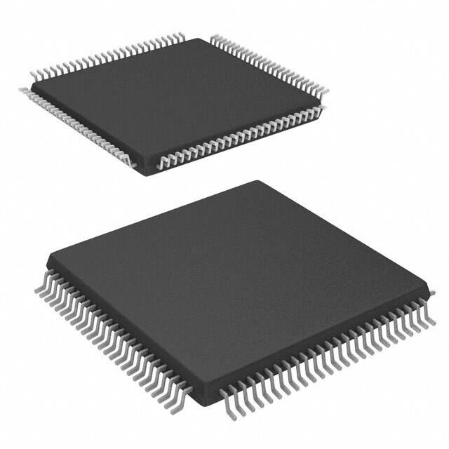


 工商网监
湘ICP备2023018690号
工商网监
湘ICP备2023018690号
