IA186EB/IA188EB
8-Bit/16-Bit Microcontrollers
As of Production Ver. 00
July 30, 2008
IA186EB/IA188EB
8-Bit/16-Bit Microcontrollers
Data Sheet
IA211080314-00
Page 1 of 80
www.Innovasic.com
Customer Support:
1-888-824-4184
�IA186EB/IA188EB
8-Bit/16-Bit Microcontrollers
Copyright
July 30, 2008
2008 by Innovasic Semiconductor, Inc.
Published by Innovasic Semiconductor, Inc.
3737 Princeton Drive NE, Suite 130, Albuquerque, NM 87107
MILES™ is a trademark Innovasic Semiconductor, Inc.
Intel is a registered trademark of Intel Corporation
IA211080314-00
Page 2 of 80
www.Innovasic.com
Customer Support:
1-888-824-4184
�IA186EB/IA188EB
8-Bit/16-Bit Microcontrollers
July 30, 2008
TABLE OF CONTENTS
1.
2.
3.
4.
5.
6.
7.
8.
9.
10.
11.
12.
Introduction.............................................................................................................................6
1.1 General Description.......................................................................................................6
1.2 Features .........................................................................................................................7
Packaging, Pin Descriptions, and Physical Dimensions .........................................................8
2.1 Packages and Pinouts ....................................................................................................8
2.1.1 IA186EB 84 PLCC Package .............................................................................9
2.1.2 IA188EB 84 PLCC Package ...........................................................................11
2.1.3 PLCC Physical Dimensions ............................................................................13
2.1.4 IA186EB 80 PQFP Package ...........................................................................14
2.1.5 IA188EB 80 PQFP Package ...........................................................................16
2.1.6 PQFP Physical Dimensions ............................................................................18
2.1.7 IA186EB 80 LQFP Package ...........................................................................19
2.1.8 IA188EB 80 LQFP Package ...........................................................................21
2.1.9 LQFP Physical Dimensions ............................................................................23
2.2 IA186EB Pin/Signal Descriptions ...............................................................................24
2.3 IA188EB Pin/Signal Descriptions ...............................................................................33
Maximum Ratings, Thermal Characteristics, and DC Parameters .......................................41
Functional Description..........................................................................................................43
4.1 Device Architecture.....................................................................................................43
4.1.1 Bus Interface Unit ...........................................................................................43
4.1.2 Clock Generator ..............................................................................................45
4.1.3 Interrupt Control Unit .....................................................................................46
4.1.4 Timer/Counter Unit ........................................................................................46
4.1.5 Serial Communications Unit...........................................................................46
4.1.6 Chip-Select Unit .............................................................................................46
4.1.7 I/O Port Unit ...................................................................................................47
4.1.8 Refresh Control Unit.......................................................................................47
4.1.9 Power Management Unit ................................................................................47
4.2 Peripheral Architecture ...............................................................................................47
4.3 Reference Documents .................................................................................................49
AC Specifications .................................................................................................................50
5.1 AC Test Conditions .....................................................................................................53
5.2 Clock Input and Clock Output Timing Characteristics ...............................................55
5.3 Serial Port Mode 0 Timing Characteristics .................................................................57
Reset Operation ....................................................................................................................58
Bus Timing ...........................................................................................................................59
Instruction Execution Times .................................................................................................69
Innovasic Part Number Cross-Reference..............................................................................75
Errata.....................................................................................................................................78
Revision History ...................................................................................................................79
For Additional Information...................................................................................................80
IA211080314-00
Page 3 of 80
www.Innovasic.com
Customer Support:
1-888-824-4184
�IA186EB/IA188EB
8-Bit/16-Bit Microcontrollers
July 30, 2008
LIST OF FIGURES
Figure 1. IA186EB 84-Pin PLCC Package Diagram ......................................................................9
Figure 2. IA188EB 84-Pin PLCC Package Diagram ....................................................................11
Figure 3. 84-Pin PLCC Physical Package Dimensions ................................................................13
Figure 4. IA186EB 80-Pin PQFP Package Diagram ....................................................................14
Figure 5. IA188EB 80-Pin PQFP Package Diagram ....................................................................16
Figure 6. 80-Pin PQFP Physical Package Dimensions .................................................................18
Figure 7. IA186EB 80-Pin LQFP Package Diagram ....................................................................19
Figure 8. IA188EB 80-Pin LQFP Package Diagram ....................................................................21
Figure 9. 80-Pin LQFP Physical Package Dimensions .................................................................23
Figure 10. IA186EB/IA188EB Functional Block Diagram ..........................................................44
Figure 11. Clock Circuit Connection Options ..............................................................................45
Figure 12. AC Input Characteristics .............................................................................................50
Figure 13. AC Output Characteristics ...........................................................................................51
Figure 14. Relative Timing Characteristics ..................................................................................52
Figure 15. AC Test Load ..............................................................................................................53
Figure 16. Typical Output Delay Variations Versus Load Capacitance .......................................54
Figure 17. Typical Rise and Fall Variations Versus Load Capacitance .......................................54
Figure 18. Clock Input and Clock Output Timing Characteristics ...............................................55
Figure 19. Serial Port Mode 0 Timing Characteristics .................................................................57
Figure 20. Cold Reset Timing.......................................................................................................60
Figure 21. Warm Reset Timing ....................................................................................................61
Figure 22. Read, Fetch, and Refresh Cycle Timing ......................................................................62
Figure 23. Write Cycle Timing .....................................................................................................63
Figure 24. Halt Cycle Timing .......................................................................................................64
Figure 25. Interrupt Acknowledge (inta1_n, inta0_n) Cycle Timing ...........................................65
Figure 26. hold/hlda Timing .........................................................................................................66
Figure 27. Refresh During Hold Acknowledge Timing ...............................................................67
Figure 28. Ready Timing ..............................................................................................................68
IA211080314-00
Page 4 of 80
www.Innovasic.com
Customer Support:
1-888-824-4184
�IA186EB/IA188EB
8-Bit/16-Bit Microcontrollers
July 30, 2008
LIST OF TABLES
Table 1. IA186EB 84-Pin PLCC Pin Listing ................................................................................10
Table 2. IA188EB 84-Pin PLCC Pin Listing ................................................................................12
Table 3. IA186EB 80-Pin PQFP Pin Listing ................................................................................15
Table 4. IA188EB 80-Pin PQFP Pin Listing ................................................................................17
Table 5. IA186EB 80-Pin LQFP Pin Listing ................................................................................20
Table 6. IA188EB 80-Pin LQFP Pin Listing ................................................................................22
Table 7. IA186EB Pin/Signal Descriptions ..................................................................................24
Table 8. IA188EB Pin/Signal Descriptions ..................................................................................33
Table 9. IA186EB and IA188EB Absolute Maximum Ratings ....................................................41
Table 10. IA186EB and IA188EB Thermal Characteristics .........................................................41
Table 11. IA186EB and IA188EB DC Parameters .......................................................................42
Table 12. Peripheral Control Block Registers ..............................................................................48
Table 13. AC Input Characteristics for 5.0-Volt Operation..........................................................50
Table 14. AC Input Characteristics for 3.3-Volt Operation..........................................................50
Table 15. AC Output Characteristics for 5.0-Volt Operation .......................................................51
Table 16. AC Output Characteristics for 3.3-Volt Operation .......................................................51
Table 17. Relative Timing Characteristics....................................................................................53
Table 18. Clock Input and Clock Output Timing Characteristics for 5.0-Volt Operation ...........55
Table 19. Clock Input and Output Characteristics for 3.3-Volt Operation ...................................56
Table 20. Serial Port Mode 0 Timing Characteristics...................................................................57
Table 21. Instruction Set Timing ..................................................................................................69
Table 22. Innovasic Part Number Cross-Reference for the PLCC ...............................................75
Table 23. Innovasic Part Number Cross-Reference for the PQFP................................................76
Table 24. Innovasic Part Number Cross-Reference for the LQFP ...............................................77
Table 25. Revision History ...........................................................................................................79
IA211080314-00
Page 5 of 80
www.Innovasic.com
Customer Support:
1-888-824-4184
�IA186EB/IA188EB
8-Bit/16-Bit Microcontrollers
1.
July 30, 2008
Introduction
The Innovasic Semiconductor IA186EB and IA188EB microcontrollers are form, fit, and
function replacements for the original Intel® 80C186EB, 80C188EB, 80L186EB, and 80L188EB
16-bit high-integration embedded processors.
These devices are produced using Innovasic’s Managed IC Lifetime Extension System
(MILES™). This cloning technology, which produces replacement ICs beyond simple
emulations, ensures complete compatibility with the original device, including any
―undocumented features.‖ Additionally, the MILES process captures the clone design in such a
way that production of the clone can continue even as silicon technology advances.
The IA186EB and IA188EB microcontrollers replace the obsolete Intel 80C186EB and
80C188EB devices, allowing users to retain existing board designs, software
compilers/assemblers, and emulation tools, thereby avoiding expensive redesign efforts.
1.1
General Description
The Innovasic Semiconductor IA186EB and IA188EB microcontrollers are an upgrade for the
80C186EB/80C188EB microcontroller designs with integrated peripherals to provide increased
functionality and reduce system costs. The IA186EB and IA188EB devices are designed to
satisfy requirements of embedded products designed for telecommunications, office automation
and storage, and industrial controls.
The IA186EB and IA188EB microcontrollers have a set of base peripherals beneficial to many
embedded applications and include a standard numeric interface, an interrupt control unit, a chipselect unit, a DRAM refresh control unit, a power management unit, and three 16-bit
timer/counters.
The IA186EB and IA188EB microcontrollers are capable of operating at 5.0 or 3.3 volts. This
datasheet discusses both modes of operation. Where applicable, characteristics specific to either
3.3 or 5.0 volt operation are identified separately throughout this datasheet.
Additionally, the IA186EB and IA188EB include two integrated serial ports that support both
synchronous and asynchronous communications, simplifying inter-processor and display
communications. The IA186EB and IA188EB also have an enhanced chip-select unit and two
multiplexed I/O ports. The enhanced chip-select unit offers 10 general chip selects, each with
the ability to address up to 1 Mbyte. This enhanced unit enables memory-bank switching to
expand the IA186EB/IA188EB 1-Mbyte address space. The I/O ports allow for basic functions
such as scanning keypads for input. The ports can also be used to control system power
consumption, disabling unneeded components.
The serial ports, I/O capabilities, and enhanced chip selects make the IA186EB/IA188EB an
excellent processor for portable data acquisition or communication applications.
IA211080314-00
Page 6 of 80
www.Innovasic.com
Customer Support:
1-888-824-4184
�IA186EB/IA188EB
8-Bit/16-Bit Microcontrollers
1.2
July 30, 2008
Features
The primary features of the IA186EB and IA188EB microcontrollers are as follows:
Low-Power Operating Modes
– Idle (freezes CPU clocks; peripherals are kept active)
– Power-Down (freezes all internal clocks)
Low-Power CPU Core (static)
Direct Addressing Capability
– Memory: 1 Mbyte
– I/O: 64 Kbyte
I/O Ports
– 2 each, 8-Bit
– Multiplexed
Clock Generator
Chip Selects
– 10 each, Programmable
– Integral Wait-State Generator
Memory Refresh Control Unit
Interrupt Controller, Programmable
Counter/Timers
– 3 each, 16-Bit
– Programmable
Serial Channels
– 2 each, UARTs
– Integral Baud Rate Generator
Operating Frequency (system clock input)
– 66.7 MHz @ 5V
– 55.5 MHz @ 3.3V
Chapter 4, Functional Description, provides details of the IA186EB and IA188EB
microcontrollers, including the features listed above.
IA211080314-00
Page 7 of 80
www.Innovasic.com
Customer Support:
1-888-824-4184
�IA186EB/IA188EB
8-Bit/16-Bit Microcontrollers
2.
July 30, 2008
Packaging, Pin Descriptions, and Physical Dimensions
Information on the packages and pin descriptions for the IA186EB and the IA188EB is provided
separately. Refer to sections, figures, and tables for information on the device of interest.
2.1
Packages and Pinouts
The Innovasic Semiconductor IA186EB and IA188EB microcontroller is available in the
following packages:
84-Pin Plastic Leaded Chip Carrier (PLCC), equivalent to original PLCC package
80-Pin Plastic Quad Flat Pack (PQFP), equivalent to original PQFP package
80-Pin Low-Profile Quad Flat Pack (LQFP), equivalent to original SQFP package
IA211080314-00
Page 8 of 80
www.Innovasic.com
Customer Support:
1-888-824-4184
�IA186EB/IA188EB
8-Bit/16-Bit Microcontrollers
2.1.1
July 30, 2008
IA186EB 84 PLCC Package
The pinout for the IA186EB 84 PLCC Package is as shown in Figure 1. The corresponding
pinout is provided in Table 1.
Figure 1. IA186EB 84-Pin PLCC Package Diagram
IA211080314-00
Page 9 of 80
www.Innovasic.com
Customer Support:
1-888-824-4184
�IA186EB/IA188EB
8-Bit/16-Bit Microcontrollers
July 30, 2008
Table 1. IA186EB 84-Pin PLCC Pin Listing
Pin
1
2
3
4
5
6
7
8
9
10
11
12
13
14
15
16
17
18
19
20
21
Name
Vcc
Vss
error_n
rd_n
wr_n
ale
bhe_n
s2_n
s1_n
s0_n
den_n
hlda
hold
test_n/busy
lock_n
dt/r_n
nmi
ready
p1.7/gcs7_n
p1.6/gcs6_n
p1.5/gcs5_n
Pin
22
23
24
25
26
27
28
29
30
31
32
33
34
35
36
37
38
39
40
41
42
Name
Vss
Vcc
p1.4/gcs4_n
p1.3/gcs3_n
p1.2/gcs2_n
p1.1/gcs1_n
p1.0/gcs0_n
lcs_n
ucs_n
int0
int1
int2/inta0_n
int3/inta1_n
int4
pdtmr
resin_n
resout
pereq
oscout
clkin
Vcc
Pin
43
44
45
46
47
48
49
50
51
52
53
54
55
56
57
58
59
60
61
62
63
Name
Vss
clkout
t0out
t0in
t1out
t1in
p2.7
p2.6
cts0_n
txd0
rxd0
p2.5/bclk0
p2.3/sint1
p2.4/cts1_n
p2.0/rxd1
p2.1/txd1
p2.2/bclk1
ncs_n
ad0
ad8
Vss
IA211080314-00
Page 10 of 80
Pin
64
65
66
67
68
69
70
71
72
73
74
75
76
77
78
79
80
81
82
83
84
Name
Vcc
Vss
ad1
ad9
ad2
ad10
ad3
ad11
ad4
ad12
ad5
ad13
ad6
ad14
ad7
ad15
a16
a17
a18
a19/once_n
Vss
www.Innovasic.com
Customer Support:
1-888-824-4184
�IA186EB/IA188EB
8-Bit/16-Bit Microcontrollers
2.1.2
July 30, 2008
IA188EB 84 PLCC Package
The pinout for the IA188EB 84 PLCC Package is as shown in Figure 2. The corresponding
pinout is provided in Table 2.
Figure 2. IA188EB 84-Pin PLCC Package Diagram
IA211080314-00
Page 11 of 80
www.Innovasic.com
Customer Support:
1-888-824-4184
�IA186EB/IA188EB
8-Bit/16-Bit Microcontrollers
July 30, 2008
Table 2. IA188EB 84-Pin PLCC Pin Listing
Pin
1
2
3
4
5
6
7
8
9
10
11
12
13
14
15
16
17
18
19
20
21
Name
Vcc
Vss
Not Connected
rd_n
wr_n
ale
rfsh_n
s2_n
s1_n
s0_n
den_n
hlda
hold
test_n
lock_n
dt/r_n
nmi
ready
p1.7/gcs7_n
p1.6/gcs6_n
p1.5/gcs5_n
Pin
22
23
24
25
26
27
28
29
30
31
32
33
34
35
36
37
38
39
40
41
42
Name
Vss
Vcc
p1.4/gcs4_n
p1.3/gcs3_n
p1.2/gcs2_n
p1.1/gcs1_n
p1.0/gcs0_n
lcs_n
ucs_n
int0
int1
int2/inta0_n
int3/inta1_n
int4
pdtmr
resin_n
resout
Not Connected
oscout
clkin
Vcc
Pin
43
44
45
46
47
48
49
50
51
52
53
54
55
56
57
58
59
60
61
62
63
Name
Vss
clkout
t0out
t0in
t1out
t1in
p2.7
p2.6
cts0_n
txd0
rxd0
p2.5/bclk0
p2.3/sint1
p2.4/cts1_n
p2.0/rxd1
p2.1/txd1
p2.2/bclk1
Not Connected
ad0
a8
Vss
IA211080314-00
Page 12 of 80
Pin
64
65
66
67
68
69
70
71
72
73
74
75
76
77
78
79
80
81
82
83
84
Name
Vcc
Vss
ad1
a9
ad2
a10
ad3
a11
ad4
a12
ad5
a13
ad6
a14
ad7
a15
a16
a17
a18
a19/once_n
Vss
www.Innovasic.com
Customer Support:
1-888-824-4184
�IA186EB/IA188EB
8-Bit/16-Bit Microcontrollers
2.1.3
July 30, 2008
PLCC Physical Dimensions
The physical dimensions for the 84 PLCC are as shown in Figure 3.
Legend:
Symbol
A
A1
D
D1
E
E1
F
F1
Min
0.165˝
0.090˝
–
–
–
–
–
–
Nom
–
–
1.190˝
1.154˝
1.190˝
1.154˝
1.110˝
1.110˝
Max
0.180˝
0.120˝
–
–
–
–
–
–
Note: The bottom package is bigger
than the top package by 0.004
inches (0.002 inches per side).
Bottom package dimensions follow
those stated in this drawing.
Figure 3. 84-Pin PLCC Physical Package Dimensions
IA211080314-00
Page 13 of 80
www.Innovasic.com
Customer Support:
1-888-824-4184
�IA186EB/IA188EB
8-Bit/16-Bit Microcontrollers
2.1.4
July 30, 2008
IA186EB 80 PQFP Package
The pinout for the IA186EB 80 PQFP Package is as shown in Figure 4. The corresponding
pinout is provided in Table 3.
Figure 4. IA186EB 80-Pin PQFP Package Diagram
IA211080314-00
Page 14 of 80
www.Innovasic.com
Customer Support:
1-888-824-4184
�IA186EB/IA188EB
8-Bit/16-Bit Microcontrollers
July 30, 2008
Table 3. IA186EB 80-Pin PQFP Pin Listing
Pin
1
2
3
4
5
6
7
8
9
10
11
12
13
14
15
16
17
18
19
20
Name
cts0_n
txd0
rxd0
p2.5/bclk0
p2.3/sint1
p2.4/cts1_n
p2.0/rxd1
p2.1/txd1
p2.2/bclk1
ad0
ad8
Vss
Vcc
Vss
ad1
ad9
ad2
ad10
ad3
ad11
Pin
21
22
23
24
25
26
27
28
29
30
31
32
33
34
35
36
37
38
39
40
Name
ad4
ad12
ad5
ad13
ad6
ad14
ad7
ad15
a16
a17
a18
a19/once_n
Vss
Vcc
Vss
rd_n
wr_n
ale
bhe_n
s2_n
Pin
41
42
43
44
45
46
47
48
49
50
51
52
53
54
55
56
57
58
59
60
Name
s1_n
s0_n
den_n
hlda
hold
test_n
lock_n
nmi
ready
p1.7/gcs7_n
p1.6/gcs6_n
p1.5/gcs5_n
Vss
Vcc
p1.4/gcs4_n
p1.3/gcs3_n
p1.2/gcs2_n
pp1.1/gcs1_n
p1.0/gcs0_n
lcs_n
IA211080314-00
Page 15 of 80
Pin
61
62
63
64
65
66
67
68
69
70
71
72
73
74
75
76
77
78
79
80
Name
ucs_n
int0
int1
int2/inta0_n
int3/inta1_n
int4
pdtmr
resin_n
resout
oscout
clkin
Vcc
Vss
clkout
t0out
t0in
t1out
t1in
p2.7
p2.6
www.Innovasic.com
Customer Support:
1-888-824-4184
�IA186EB/IA188EB
8-Bit/16-Bit Microcontrollers
2.1.5
July 30, 2008
IA188EB 80 PQFP Package
The pinout for the IA188EB 80 PQFP Package is as shown in Figure 5. The corresponding
pinout is provided in Table 4.
Figure 5. IA188EB 80-Pin PQFP Package Diagram
IA211080314-00
Page 16 of 80
www.Innovasic.com
Customer Support:
1-888-824-4184
�IA186EB/IA188EB
8-Bit/16-Bit Microcontrollers
July 30, 2008
Table 4. IA188EB 80-Pin PQFP Pin Listing
Pin
1
2
3
4
5
6
7
8
9
10
11
12
13
14
15
16
17
18
19
20
Name
cts0_n
txd0
rxd0
p2.5/bclk0
p2.3/sint1
p2.4/cts1_n
p2.0/rxd1
p2.1/txd1
p2.2/bclk1
ad0
a8
Vss
Vcc
Vss
ad1
a9
ad2
a10
ad3
a11
Pin
21
22
23
24
25
26
27
28
29
30
31
32
33
34
35
36
37
38
39
40
Name
ad4
a12
ad5
a13
ad6
a14
ad7
a15
a16
a17
a18
a19/once_n
Vss
Vcc
Vss
rd_n
wr_n
ale
rfsh_n
s2_n
Pin
41
42
43
44
45
46
47
48
49
50
51
52
53
54
55
56
57
58
59
60
Name
s1_n
s0_n
den_n
hlda
hold
test_n
lock_n
nmi
ready
p1.7/gcs7_n
p1.6/gcs6_n
p1.5/gcs5_n
Vss
Vcc
p1.4/gcs4_n
p1.3/gcs3_n
p1.2/gcs2_n
pp1.1/gcs1_n
p1.0/gcs0_n
lcs_n
IA211080314-00
Page 17 of 80
Pin
61
62
63
64
65
66
67
68
69
70
71
72
73
74
75
76
77
78
79
80
Name
ucs_n
int0
int1
int2/inta0_n
int3/inta1_n
int4
pdtmr
resin_n
resout
oscout
clkin
Vcc
Vss
clkout
t0out
t0in
t1out
t1in
p2.7
p2.6
www.Innovasic.com
Customer Support:
1-888-824-4184
�IA186EB/IA188EB
8-Bit/16-Bit Microcontrollers
2.1.6
July 30, 2008
PQFP Physical Dimensions
The physical dimensions for the 80 PQFP are as shown in Figure 6.
Legend:
Notes:
1. Dimension D1 and E1 do not include mold protrusion.
Allowable protrusion is 0.25mm per side. Dimension D1
and E1 do not include mold mismatch and are determined
a datum plane –H– .
2. Dimension b does not include dambar protrusion.
Allowable dambar protrusion will not cause the lead width
to exceed the maximum b dimension by more than
0.08mm. Dambar cannot be located on the lower radius of
the lead foot.
Millimeter
Inch
Symbol Min Nom Max Min Nom Max
A
–
– 3.40 –
– 0.134
A1
0.25 –
– 0.010 –
–
A2
2.55 2.72 3.05 0.100 0.107 0.120
D
23.90 Basic
0.941 Basic
D1
20.00 Basic
0.787 Basic
E
17.90 Basic
0.705 Basic
E1
14.00 Basic
0.551 Basic
R2 0.013 – 0.30 0.005 – 0.012
R1 0.013 –
– 0.005 –
–
θ
0° 3.5° 7° 0° 3.5° 7°
θ1
0°
–
–
0°
–
–
a
7°
REF
7°
REF
θ2, θ3
15° REF
15° REF
θ2, θ3b
c
0.11 0.15 0.23 0.004 0.006 0.009
L
0.73 0.88 1.03 0.029 0.035 0.041
L1
1.95 REF
0.077 REF
S
0.40 –
– 0.016 –
–
b
0.30 0.35 0.45 0.012 0.014 0.018
e
0.80 BSC
0.031 BSC
D2
18.40 REF
0.724
E2
12.00 REF
0.472
Tolerances of Form and Position
aaa
0.25
0.010
bbb
0.20
0.008
ccc
0.20
0.008
aAlloy 42 L/F.
bCopper L/F.
Figure 6. 80-Pin PQFP Physical Package Dimensions
IA211080314-00
Page 18 of 80
www.Innovasic.com
Customer Support:
1-888-824-4184
�IA186EB/IA188EB
8-Bit/16-Bit Microcontrollers
2.1.7
July 30, 2008
IA186EB 80 LQFP Package
The pinout for the IA186EB 80 LQFP Package is as shown in Figure 7. The corresponding
pinout is provided in Table 5.
Figure 7. IA186EB 80-Pin LQFP Package Diagram
IA211080314-00
Page 19 of 80
www.Innovasic.com
Customer Support:
1-888-824-4184
�IA186EB/IA188EB
8-Bit/16-Bit Microcontrollers
July 30, 2008
Table 5. IA186EB 80-Pin LQFP Pin Listing
Pin
1
2
3
4
5
6
7
8
9
10
11
12
13
14
15
16
17
18
19
20
Name
hlda
hold
test_n
lock_n
nmi
ready
p1.7/gcs7_n
p1.6/gcs6_n
p1.5/gcs5_n
Vss
Vcc
p1.4/gcs4_n
p1.3/gcs3_n
p1.2/gcs2_n
p1.1/gcs1_n
p1.0/gcs0_n
lcs_n
ucs_n
int0
int1
Pin
21
22
23
24
25
26
27
28
29
30
31
32
33
34
35
36
37
38
39
40
Name
int2/inta0_n
int3/inta1_n
int4
pdtmr
resin_n
resout
oscout
clkin
Vcc
Vss
clkout
t0out
t0in
t1out
t1in
p2.7
p2.6
cts0_n
txd0
rxd0
Pin
41
42
43
44
45
46
47
48
49
50
51
52
53
54
55
56
57
58
59
60
Name
p2.5/bclk0
p2.3/sint1
p2.4/cts1_n
p2.0/rxd1
p2.1/txd1
p2.2/bclk1
ad0
ad8
Vss
Vcc
Vss
ad1
ad9
ad2
ad10
ad3
ad11
ad4
ad12
ad5
IA211080314-00
Page 20 of 80
Pin
61
62
63
64
65
66
67
68
69
70
71
72
73
74
75
76
77
78
79
80
Name
ad13
ad6
ad14
ad7
ad15
a16
a17
a18
a19/once_n
Vss
Vcc
Vss
rd_n
wr_n
ale
bhe_n
s2_n
s1_n
s0_n
den_n
www.Innovasic.com
Customer Support:
1-888-824-4184
�IA186EB/IA188EB
8-Bit/16-Bit Microcontrollers
2.1.8
July 30, 2008
IA188EB 80 LQFP Package
The pinout for the IA188EB 80 LQFP Package is as shown in Figure 8. The corresponding
pinout is provided in Table 6.
Figure 8. IA188EB 80-Pin LQFP Package Diagram
IA211080314-00
Page 21 of 80
www.Innovasic.com
Customer Support:
1-888-824-4184
�IA186EB/IA188EB
8-Bit/16-Bit Microcontrollers
July 30, 2008
Table 6. IA188EB 80-Pin LQFP Pin Listing
Pin
1
2
3
4
5
6
7
8
9
10
11
12
13
14
15
16
17
18
19
20
Name
hlda
hold
test_n
lock_n
nmi
ready
p1.7/gcs7_n
p1.6/gcs6_n
p1.5/gcs5_n
Vss
Vcc
p1.4/gcs4_n
p1.3/gcs3_n
p1.2/gcs2_n
p1.1/gcs1_n
p1.0/gcs0_n
lcs_n
ucs_n
int0
int1
Pin
21
22
23
24
25
26
27
28
29
30
31
32
33
34
35
36
37
38
39
40
Name
int2/inta0_n
int3/inta1_n
int4
pdtmr
resin_n
resout
oscout
clkin
Vcc
Vss
clkout
t0out
t0in
t1out
t1in
p2.7
p2.6
cts0_n
txd0
rxd0
Pin
41
42
43
44
45
46
47
48
49
50
51
52
53
54
55
56
57
58
59
60
Name
p2.5/bclk0
p2.3/sint1
p2.4/cts1_n
p2.0/rxd1
p2.1/txd1
p2.2/bclk1
ad0
ad8
Vss
Vcc
Vss
ad1
ad9
ad2
ad10
ad3
ad11
ad4
ad12
ad5
IA211080314-00
Page 22 of 80
Pin
61
62
63
64
65
66
67
68
69
70
71
72
73
74
75
76
77
78
79
80
Name
ad13
ad6
ad14
ad7
ad15
a16
a17
a18
a19/once_n
Vss
Vcc
Vss
rd_n
wr_n
ale
bhe_n
s2_n
s1_n
s0_n
den_n
www.Innovasic.com
Customer Support:
1-888-824-4184
�IA186EB/IA188EB
8-Bit/16-Bit Microcontrollers
2.1.9
July 30, 2008
LQFP Physical Dimensions
The physical dimensions for the 80 LQFP are as shown in Figure 9.
Legend:
Symbol
A
A1
A2
b
b1
c
c1
D
D1
E
E1
e
L
L1
R1
R2
S
θ
θ1
θ2
θ3
Dimension in mm
Min Nom Max
–
–
1.60
0.05
–
0.15
1.35 1.40 1.45
0.17 0.22 0.27
0.17 0.20 0.23
0.09
–
0.20
0.09
–
0.16
14.00 BSC
12.00 BSC
14.00 BSC
12.00 BSC
0.50 BSC
0.45 0.60 0.75
1.00 REF
0.08
–
–
0.08
–
0.20
0.20
–
–
0°
3.5°
7°
0°
–
–
11°
12°
13°
11°
12°
13°
Dimension in Inch
Min
Mom
Max
–
–
0.063
0.002
–
0.006
0.053 0.055 0.057
0.007 0.009 0.011
0.007 0.008 0.009
0.004
–
0.008
0.004
–
0.006
0.551 BSC
0.472 BSC
0.551 BSC
0.472 BSC
0.020 BSC
0.018 0.024 0.030
0.039 REF
0.003
–
–
0.003
–
0.008
0.008
–
–
0°
3.5°
7°
0°
–
–
11°
12°
13°
11°
12°
13°
1. To be determined at seating plane C.
2. Dimensions D1 and E1 do not include
mold protrusion. D1 and E1 are
maximum plastic body size
dimensions including mold mismatch.
3. Dimension b does not include dambar
protrusion. Dambar cannot be located
on the lower radius of the foot.
4. Exact shape of each corner is
optional.
5. These dimensions apply to the flat
section of the lead between 0.10 and
0.25mm from the lead tip.
6. A1 is defined as the distance from the
seating plane to the lowest point of the
package body.
Notes:
1. Exact shape of each corner is optional.
2. Controlling dimension: mm.
Figure 9. 80-Pin LQFP Physical Package Dimensions
IA211080314-00
Page 23 of 80
www.Innovasic.com
Customer Support:
1-888-824-4184
�IA186EB/IA188EB
8-Bit/16-Bit Microcontrollers
2.2
July 30, 2008
IA186EB Pin/Signal Descriptions
Descriptions of the pin and signal functions for the IA186EB microcontroller are provided in
Table 7.
Several of the IA186EB pins have different functions depending on the operating mode of the
device. Each of the different signals supported by a pin is listed and defined in Table 7—
indexed alphabetically in the first column of the table. Additionally, the name of the pin
associated with the signal as well as the pin numbers for the PLCC, LQFP, and PQFP packages
are provided in the ―Pin‖ column. If the signal and pin names are the same, a dash is provided in
the ―Pin-Name‖ column. Signals not used in a specific package type are designated ―NA.‖
Table 7. IA186EB Pin/Signal Descriptions
Signal
a16
Name
a16
Pin
PLCC
80
PQFP
66
LQFP
29
a17
a17
81
67
30
a18
a18
82
68
31
a19
a19/once_n
83
69
32
ad0
ad1
ad2
ad3
ad4
ad5
ad6
ad7
ad8
ad9
ad10
ad11
ad12
ad13
ad14
ad15
ad0
ad1
ad2
ad3
ad4
ad5
ad6
ad7
ad8
ad9
ad10
ad11
ad12
ad13
ad14
ad15
61
66
68
70
72
74
76
78
62
67
69
71
73
75
77
79
47
52
54
56
58
60
62
64
48
53
55
57
59
61
63
65
10
15
17
19
21
23
25
27
11
16
18
20
22
24
26
28
Description
address Bits [16–19]. Input/Output. These pins
provide the four most-significant bits of the
Address Bus. During the address portion of the
IA186EB bus cycle, Address Bits [16–19] are
presented on the bus and can be latched using
the ale signal (see table entry). During the data
portion of the IA186EB bus cycle, these lines
are driven to a logic 0.
address/data Bits [0–15]. Input/Output. These
pins provide the multiplexed Address Bus and
Data Bus. During the address portion of the
IA186EB bus cycle, Address Bits [0–15] are
presented on the bus and can be latched using
the ale signal (see next table entry). During the
data portion of the IA186EB bus cycle, 8- or
16-bit data are present on these lines.
IA211080314-00
Page 24 of 80
www.Innovasic.com
Customer Support:
1-888-824-4184
�IA186EB/IA188EB
8-Bit/16-Bit Microcontrollers
July 30, 2008
Table 7. IA186EB Pin/Signal Descriptions (Continued)
Signal
ale
Name
ale
Pin
PLCC
6
PQFP
75
LQFP
38
bclk0
p2.5/bclk0
54
41
4
bclk1
p2.2/bclk1
59
46
9
bhe_n
bhe_n
7
76
39
bhe_n is
multiplexed
with
refresh_n
bhe_n is
multiplexed with
refresh_n
busy
test_n/busy
Description
address latch enable. Output. Active High.
This signal is used to latch the address
information during the address portion of a bus
cycle.
baud clock, Serial Port 0. Input. The bclk0 pin
can be used to provide an alternate clock
source for Serial Port 0. The input clock rate
cannot be greater than one-half the operating
frequency of the IA186EB.
baud clock, Serial Port 1. Input. The bclk1 pin
can be used to provide an alternate clock
source for Serial Port 1. The input clock rate
cannot be greater than one-half the operating
frequency of the IA186EB.
byte high enable. Output. Active Low. When
bhe_n is asserted (low), it indicates that the
bus cycle in progress is transferring data over
the upper half of the data bus.
Additionally, bhe_n and ad0 encode the
following bus information:
14
3
46
ad0
bhe_n
0
0
1
1
0
1
0
1
Bus Status
Word Transfer
Even Byte Transfer
Odd Byte Transfer
Refresh Operation
Note: bhe_n is multiplexed with refresh_n.
busy. Input. Active High. When the busy
input is asserted, it causes the IA186EB to
suspend operation during the execution of the
Intel 80C187 Numerics Coprocessor
instructions. Operation resumes when the pin
is sampled low.
IA211080314-00
Page 25 of 80
www.Innovasic.com
Customer Support:
1-888-824-4184
�IA186EB/IA188EB
8-Bit/16-Bit Microcontrollers
July 30, 2008
Table 7. IA186EB Pin/Signal Descriptions (Continued)
Signal
clkin
Name
clkin
Pin
PLCC
41
PQFP
28
LQFP
71
clkout
clkout
44
31
74
cts0_n
cts0_n
51
38
1
cts1_n
p2.4/cts1_n
56
43
6
den_n
den_n
11
80
43
dt/r_n
dt/r_n
16
NA
NA
error_n
error_n
3
NA
NA
Description
clock input. Input. The clkin pin is the input
connection for an external clock. An external
oscillator operating at two times the required
processor operating frequency can be
connected to this pin.
If a crystal is used to supply the clock, it is
connected between the clkin pin and the
oscout pin (see oscout table entry). When a
crystal is connected, it drives an internal Pierce
oscillator to the IA186EB.
clock output. Output. The clkout pin provides
a timing reference for inputs and outputs of the
IA186EB. This clock output is one-half the
input clock (clkin) frequency. The clkout
signal has a 50% duty cycle, transitioning every
falling edge of clkin.
clear to send, Serial Port 0. Input. Active Low.
When this input is high (i.e., not asserted), data
transmission from Serial Port 0 is inhibited.
When the signal is asserted (low), data
transmission is permitted.
clear to send, Serial Port 1. Input. Active Low.
When this input is high (i.e., not asserted), data
transmission from Serial Port 1 is inhibited.
When the signal is asserted (low), data
transmission is permitted.
data enable. Output. Active Low. This signal
is used to enable of bidirectional transceivers in
a buffered system. The den_n signal is
asserted (low) only when data are to be
transferred on the bus.
data transmit/receive. Output. This signal is
used to control the direction of data flow for
bidirectional buffers in a buffered system.
When dt/r_n is high, the direction indicated is
transmit; when dt/t_n is low, the direction
indicated is receive.
error. Input. Active Low. When this signal is
asserted (low), it indicates that the last
numerics coprocessor operation resulted in an
exception condition.
IA211080314-00
Page 26 of 80
www.Innovasic.com
Customer Support:
1-888-824-4184
�IA186EB/IA188EB
8-Bit/16-Bit Microcontrollers
July 30, 2008
Table 7. IA186EB Pin/Signal Descriptions (Continued)
Signal
gcs0_n
gcs1_n
gcs2_n
gcs3_n
gcs4_n
gcs5_n
gcs6_n
gcs7_n
hlda
Name
p1.0/gcs0_n
p1.1/gcs1_n
p1.2/gcs2_n
p1.3/gcs3_n
p1.4/gcs4_n
p1.5/gcs5_n
p1.6/gcs6_n
p1.7/gcs7_n
hlda
Pin
PLCC
28
27
26
25
24
21
20
19
12
PQFP
16
15
14
13
12
9
8
7
1
LQFP
59
58
57
56
55
52
51
50
44
hold
hold
13
2
45
int0
(input)
int1
(input)
int0 (input)
31
19
62
int1
(input)
32
20
63
int2
int2/inta0_n
33
21
64
int3
int3/inta1_n
34
22
65
int4
(input)
int4
(input)
35
23
66
inta0_n
int2/inta0_n
33
21
64
Description
generic chip select n (n = 0–7). Output. Active
Low. When programmed and enabled, each of
these pins provide a chip select signal that will
be asserted (low) whenever the address of a
memory or I/O bus cycle is within the address
space programmed for that output.
hold acknowledge. Output. Active High.
When hlda is asserted (high), it indicates that
the IA186EB has relinquished control of the
local bus to another bus master in response to
a HOLD request (see next table entry).
When hlda is asserted, the IA186EB data bus
and control signals are floated, allowing another
bus master to drive the signals directly.
hold. Input. Active High. This signal is a
request indicating that an external bus master
wishes to gain control of the local bus. The
IA186EB will relinquish control of the local bus
between instruction boundaries not conditioned
by a LOCK prefix.
interrupt n (n = 04). Input/Output. Active
High. These maskable inputs interrupt program
flow and cause execution to continue at an
interrupt vector of a specific interrupt type as
follows:
int0:
int1:
int2:
int3:
int4:
Type 12
Type 13
Type 14
Type 15
Type 17
To allow interrupt expansion, int0 and int1 can
be used with the interrupt acknowledge signals
inta0_n and inta1_n (see next table entries) to
serve as external interrupt inputs or interrupt
acknowledge outputs.
interrupt acknowledge 0. Input/Output. Active
Low. This pin provides an interrupt
acknowledge handshake in response to an
interrupt request on the int0 pin (see previous
table entry).
IA211080314-00
Page 27 of 80
www.Innovasic.com
Customer Support:
1-888-824-4184
�IA186EB/IA188EB
8-Bit/16-Bit Microcontrollers
July 30, 2008
Table 7. IA186EB Pin/Signal Descriptions (Continued)
Signal
inta1_n
Name
int3/inta1_n
Pin
PLCC
34
PQFP
22
LQFP
65
lcs_n
lcs_n
29
17
60
lock_n
lock_n
15
4
47
ncs_n
ncs_n
60
NA
NA
nmi
nmi
17
5
48
once_n
a19/once_n
83
69
32
Description
interrupt acknowledge 1. Input/Output. Active
Low. This pin provides an interrupt
acknowledge handshake in response to an
interrupt request on the int1 pin (see previous
table entry).
lower chip select. Output. Active Low. This
pin provides a chip select signal that will be
asserted (low) whenever the address of a
memory bus cycle is within the address space
programmed for that output.
lock. Output. Active Low. When asserted
(low), this signal indicates that the bus cycle in
progress is cannot be interrupted. While
lock_n is active, the IA186EB will not service
bus requests such as HOLD.
When resin_n is active, this pin is weakly held
high and must not be driven low.
numerics coprocessor select. Output. Active
Low. This signal is asserted (low) when the
IA186EB accesses an Intel 80C187 Numerics
Coprocessor.
non-maskable interrupt. Input. Active High.
When the nmi signal is asserted (high) it
causes a Type 2 interrupt to be serviced by the
IA186EB.
Note: The assertion of nmi is latched internally
by the IA186EB.
on-circuit emulation. Input. Active Low. Note:
ONCE Mode is used for device testing.
If the once_n pin is driven low during a reset
operation, all IA186EB output and input/output
pins are placed in a high-impedance state.
This pin is weakly held high while resin_n is
active.
IA211080314-00
Page 28 of 80
www.Innovasic.com
Customer Support:
1-888-824-4184
�IA186EB/IA188EB
8-Bit/16-Bit Microcontrollers
July 30, 2008
Table 7. IA186EB Pin/Signal Descriptions (Continued)
Signal
oscout
Name
oscout
Pin
PLCC
40
PQFP
27
LQFP
70
p1.0
p1.1
p1.2
p1.3
p1.4
p1.5
p1.6
p1.7
p2.0
p1.0/gcs0_n
p1.1/gcs1_n
p1.2/gcs2_n
p1.3/gcs3_n
p1.4/gcs4_n
p1.5/gcs5_n
p1.6/gcs6_n
p1.7/gcs7_n
p2.0/rxd1
28
27
26
25
24
21
20
19
57
16
15
14
13
12
9
8
7
44
59
58
57
56
55
52
51
50
7
p2.1
p2.1/txd1
58
45
8
p2.2
p2.2/bclk1
59
46
9
p2.3
p2.3/sint1
55
42
5
p2.4
p2.4/cts1_n
56
43
6
p2.5
p2.5/bclk0
54
41
4
p2.6
p2.6
50
37
80
p2.7
p2.7
49
36
79
Description
oscillator output. Output. The oscout pin is
the output connection for an external crystal
that drives the IA186EB internal Pierce
oscillator. (When an external crystal is used, it
is connected between this pin and the clkin pin.
See clkin table entry.)
Note: If an external oscillator or clock source is
used to drive the IA186EB instead of a crystal,
oscout must be left unconnected (i.e., must be
floated). When the IA186EB is operating in the
ONCE mode, oscout does not float.
port 1, Bit [N] (N = 0–7). Output. Each pin of
Port 1, p1.0–p1.7, can function individually as a
general-purpose output line.
port 2, Bit [0]. Input. This pin functions as a
general-purpose input line.
port 2, Bit [1]. Output. This pin functions as a
general-purpose output line.
port 2, Bit [2]. Input. This pin functions as a
general-purpose input line.
port 2, Bit [3]. Output. This pin functions as a
general-purpose output line.
port 2, Bit [4]. Input. This pin functions as a
general-purpose input line.
port 2, Bit [5]. Input. This pin functions as a
general-purpose input line.
port 2, Bit [6]. Input/Output (open drain). This
pin functions as a general-purpose bidirectional
input/output line.
port 2, Bit [7]. Input/Output (open drain). This
pin functions as a general-purpose bidirectional
input/output line.
IA211080314-00
Page 29 of 80
www.Innovasic.com
Customer Support:
1-888-824-4184
�IA186EB/IA188EB
8-Bit/16-Bit Microcontrollers
July 30, 2008
Table 7. IA186EB Pin/Signal Descriptions (Continued)
Signal
pdtmr
Name
pdtmr
Pin
PLCC
36
PQFP
24
LQFP
67
Description
power-down timer. Input/Output (push-pull).
Note: The IA186EB enters Powerdown Mode
when the PWRDN bit in the Power Control
Register is set to 1 and a HALT instruction is
executed. Exit from the Powerdown Mode
occurs upon receipt of a non-maskable interrupt
(i.e., assertion of the nmi input) or a reset (i.e.,
assertion of the resin_n input).
The pdtmr pin, which is normally connected to
an external capacitor, determines the amount of
time that the IA186EB waits before resuming
normal operation after an exit from the
Powerdown when a non-maskable interrupt is
received—essentially a delay between the
assertion of the nmi input and the enabling of
the IA186EB internal clocks. The delay
required depends on the start-up characteristics
of the crystal oscillator.
pereq
pereq
39
NA
NA
rd_n
rd_n
4
73
36
ready
ready
18
6
49
resin_n
resin_n
37
25
68
The pdtmr pin does not apply when the
Powerdown Mode is exited by the receipt of a
reset (i.e., the assertion resin_n).
numerics coprocessor external request. Input.
Active High. When asserted (high), this signal
indicates that a data transfer between an Intel
80C187 Numerics Coprocessor.and memory is
pending.
read. Output. Active Low. When asserted
(low), rd_n indicates that the accessed memory
or I/O device must drive data from the location
being accessed onto the data bus.
ready. Input. Active High. When asserted
(high) the ready line indicates a bus-cycle
completion. This signal must be active to
terminate any bus cycle unless the IA186EB
Chip-Select Unit is being used, in which case,
ready is ignored.
reset input. Input. Active Low. When resin_n
is asserted (low), the IA186EB immediately
terminates any bus cycle in progress and
assumes an initialized state. All pins are driven
to a known state, and resout (see next table
entry) is asserted.
IA211080314-00
Page 30 of 80
www.Innovasic.com
Customer Support:
1-888-824-4184
�IA186EB/IA188EB
8-Bit/16-Bit Microcontrollers
July 30, 2008
Table 7. IA186EB Pin/Signal Descriptions (Continued)
Signal
resout
Name
resout
Pin
PLCC
38
PQFP
26
LQFP
69
rxd0
rxd0
53
40
3
rxd1
p2.0/rxd1
57
44
7
s0_n
s0_n
10
79
42
s1_n
s1_n
9
78
41
s2_n
s2_n
8
77
40
sint1
p2.3/sint1
55
42
5
t0in
t0in
46
33
76
t0out
t0out
45
32
75
t1in
t1in
48
35
78
Description
reset output. Output. Active High. When
resout is asserted, it indicates that the
IA186EB is being reset. The resout signal will
remain active (high) as long as resin_n
remains active (low).
Receive (rx) data, Serial Port 0. Input/Output.
This pin is the serial data input for Serial Port 0.
During synchronous serial communications,
rxd0 is bidirectional and functions an output for
data transmission (txd0 becomes the clock).
Receive (rx) data, Serial Port 1. Input/Output.
This pin is the serial data input for Serial Port 1.
During synchronous serial communications,
rxd0 is bidirectional and functions an output for
data transmission (txd0 becomes the clock).
status (n = 0–2). Output. During a bus cycle
the status (i.e., type) of cycle is encoded on
these lines as follows:
s2_n s1_n s0_n Bus Cycle Status
0
0
0
Interrupt Acknowledge
0
0
1
Read I/O
0
1
0
Write I/O
0
1
1
Processor HALT
1
0
0
Queue Instruction Fetch
1
0
1
Read Memory
1
1
0
Write Memory
1
1
1
No Bus Activity
serial interrupt, Serial Port 1. Output. Active
High. When sint1 is asserted (high), it
indicates that Serial Port 1 requires service.
timer 0 input. Input. Depending on the Timer
Mode programmed for Timer 0, this input is
used either as clock input or a control signal.
timer 0 output. Output. Depending on the
Timer Mode programmed for Timer 0, this
output can provide a single clock or a
continuous waveform.
timer 1 input. Input. Depending on the Timer
Mode programmed for Timer 1, this input is
used either as clock input or a control signal.
IA211080314-00
Page 31 of 80
www.Innovasic.com
Customer Support:
1-888-824-4184
�IA186EB/IA188EB
8-Bit/16-Bit Microcontrollers
July 30, 2008
Table 7. IA186EB Pin/Signal Descriptions (Continued)
Signal
t1out
Name
t1out
Pin
PLCC
47
PQFP
34
LQFP
77
test_n
test_n/busy
14
3
46
txd0
txd0
52
39
2
txd1
p2.1/txd1
58
45
8
ucs_n
ucs_n
30
18
61
vcc
vcc
1, 23,
42, 64
11, 29,
50, 71
13, 34,
54, 72
vss
vss
wr_n
wr_n
2, 22,
43, 63,
65, 84
5
10, 30,
49, 51,
70, 72
74
12, 14,
33, 35,
53, 73
37
Description
timer 1 output. Output. Depending on the
Timer Mode programmed for Timer 1, this
output can provide a single clock or a
continuous waveform.
test. Input. Active Low. When the test_n
input is high (i.e., not asserted), it causes the
IA186EB to suspend operation during the
execution of the WAIT instruction. Operation
resumes when the pin is sampled low
(asserted).
Transmit (tx) data, Serial Port 0. Output. This
pin is the serial data output for Serial Port 0.
During synchronous serial communications,
txd0 becomes the transmit clock (rxd0
functions as an output for data transmission).
Transmit (tx) data, Serial Port 1. Output. This
pin is the serial data output for Serial Port 1.
During synchronous serial communications,
txd0 becomes the transmit clock (rxd1
functions as an output for data transmission).
upper chip select. Output. Active Low. This
pin provides a chip select signal that will be
asserted (low) whenever the address of a
memory bus cycle is within the address space
programmed for that output.
Power (vcc). This pin provides power for the
IA186EB device. It must be connected to a
+5V DC power source.
Ground (vss). This pin provides the digital
ground (0V) for the IA186EB. It must be
connected to a vss board plane.
write. Output. Active Low. When asserted
(low), wr_n indicates that data available on the
data bus are to be latched into the accessed
memory or I/O device.
IA211080314-00
Page 32 of 80
www.Innovasic.com
Customer Support:
1-888-824-4184
�IA186EB/IA188EB
8-Bit/16-Bit Microcontrollers
2.3
July 30, 2008
IA188EB Pin/Signal Descriptions
Descriptions of the pin and signal functions for the IA188EB microcontroller are provided in
Table 8.
Several of the IA188EB pins have different functions depending on the operating mode of the
device. Each of the different signals supported by a pin is listed and defined in Table 8—
indexed alphabetically in the first column of the table. Additionally, the name of the pin
associated with the signal as well as the pin numbers for the PLCC, LQFP, and LQFP packages
are provided in the ―Pin‖ column. If the signal and pin names are the same, no entry is provided
in the ―Pin-Name‖ column.
Table 8. IA188EB Pin/Signal Descriptions
Signal
a8
a9
a10
a11
a12
a13
a14
a15
a16
a17
a18
a19
ad0
ad1
ad2
ad3
ad4
ad5
ad6
ad7
ale
Name
a8
a9
a10
a11
a12
a13
a14
a15
a16
a17
a18
a19/once_n
ad0
ad1
ad2
ad3
ad4
ad5
ad6
ad7
ale
Pin
PLCC
62
67
69
71
73
75
77
79
80
81
82
83
61
66
68
70
72
74
76
78
6
PQFP
48
53
55
57
59
61
63
65
66
67
68
69
47
52
54
56
58
60
62
64
75
LQFP
11
16
18
20
22
24
26
28
29
30
31
32
10
15
17
19
21
23
25
27
38
bclk0
p2.5/bclk0
54
41
4
Description
address Bits [819]. Input/Output. These pins
provide the 12 most-significant bits of the
Address Bus. During the entire IA188EB bus
cycle, Address Bits [8–19] are presented on the
bus and can be latched using the ale signal
(see table entry).
address/data Bits [0–7]. Input/Output. These
pins provide a multiplexed Address Bus and
Data Bus. During the address portion of the
IA188EB bus cycle, Address Bits [0–7] are
presented on the bus and can be latched using
the ale signal (see next table entry). During the
data portion of the IA188EB bus cycle, 8-bit
data are present on these lines.
address latch enable. Output. Active High.
This signal is used to latch the address
information during the address portion of a bus
cycle.
baud clock, Serial Port 0. Input. The bclk0 pin
can be used to provide an alternate clock
source for Serial Port 0. The input clock rate
cannot be greater than one-half the operating
frequency of the IA188EB.
IA211080314-00
Page 33 of 80
www.Innovasic.com
Customer Support:
1-888-824-4184
�IA186EB/IA188EB
8-Bit/16-Bit Microcontrollers
July 30, 2008
Table 8. IA188EB Pin/Signal Descriptions (Continued)
Signal
bclk1
Name
p2.2/bclk1
Pin
PLCC
59
PQFP
46
LQFP
9
clkin
clkin
41
28
71
clkout
clkout
44
31
74
cts0_n
cts0_n
51
38
1
cts1_n
p2.4/cts1_n
56
43
6
den_n
den_n
11
80
43
dt/r_n
dt/r_n
16
NA
NA
Description
baud clock, Serial Port 1. Input. The bclk1 pin
can be used to provide an alternate clock
source for Serial Port 1. The input clock rate
cannot be greater than one-half the operating
frequency of the IA188EB.
clock input. Input. The clkin pin is the input
connection for an external clock. An external
oscillator, operating at two times the required
processor operating frequency, can be
connected to this pin.
If a crystal is used to supply the clock, it is
connected between the clkin pin and the
oscout pin (see oscout table entry). When a
crystal is connected, it drives an internal Pierce
oscillator to the IA188EB.
clock output. Output. The clkout pin provides
a timing reference for inputs and outputs of the
IA188EB. This clock output is one-half the input
clock (clkin) frequency. The clkout signal has
a 50% duty cycle, transitioning every falling
edge of clkin.
clear to send, Serial Port 0. Input. Active Low.
When this input is high (i.e., not asserted), data
transmission from Serial Port 0 is inhibited.
When the signal is asserted (low), data
transmission is permitted.
clear to send, Serial Port 1. Input. Active Low.
When this input is high (i.e., not asserted), data
transmission from Serial Port 1 is inhibited.
When the signal is asserted (low), data
transmission is permitted.
data enable. Output. Active Low. This signal
is used to enable of bidirectional transceivers in
a buffered system. The den_n signal is
asserted (low) only when data are to be
transferred on the bus.
data transmit/receive. Output. This signal is
used to control the direction of data flow for
bidirectional buffers in a buffered system.
When dt/r_n is high, the direction indicated is
transmit; when dt/t_n is low, the direction
indicated is receive.
IA211080314-00
Page 34 of 80
www.Innovasic.com
Customer Support:
1-888-824-4184
�IA186EB/IA188EB
8-Bit/16-Bit Microcontrollers
July 30, 2008
Table 8. IA188EB Pin/Signal Descriptions (Continued)
Signal
gcs0_n
gcs1_n
gcs2_n
gcs3_n
gcs4_n
gcs5_n
gcs6_n
gcs7_n
hlda
Name
p1.0/gcs0_n
p1.1/gcs1_n
p1.2/gcs2_n
p1.3/gcs3_n
p1.4/gcs4_n
p1.5/gcs5_n
p1.6/gcs6_n
p1.7/gcs7_n
hlda
Pin
PLCC
28
27
26
25
24
21
20
19
12
PQFP
16
15
14
13
12
9
8
7
1
LQFP
59
58
57
56
55
52
51
50
44
hold
(input)
hold
(input)
13
2
45
int0
(input)
int1
(input)
int0
(input)
int1
(input)
31
19
62
32
20
63
int2
int2/inta0_n
33
21
64
int3
int3/inta1_n
34
22
65
int4 (input)
int4 (input)
35
23
66
inta0_n
int2/inta0_n
33
21
64
Description
generic chip select n (n = 0–7). Output. Active
Low. When programmed and enabled, each of
these pins provide a chip select signal that will
be asserted (low) whenever the address of a
memory or I/O bus cycle is within the address
space programmed for that output.
hold acknowledge. Output. Active High.
When hlda is asserted (high), it indicates that
the IA188EB has relinquished control of the
local bus to another bus master in response to
a HOLD request (see next table entry).
When hlda is asserted, the IA188EB data bus
and control signals are floated, allowing another
bus master to drive the signals directly.
hold. Input. Active High. This signal is a
request indicating that an external bus master
wishes to gain control of the local bus. The
IA188EB will relinquish control of the local bus
between instruction boundaries not conditioned
by a lock prefix.
interrupt N (N = 0–4). Input/Output. Active
High. These maskable inputs interrupt program
flow and cause execution to continue at an
interrupt vector of a specific interrupt type as
follows:
int0:
int1:
int2:
int3:
int4:
Type 12
Type 13
Type 14
Type 15
Type 17
To allow interrupt expansion, int0 and int1 can
be used with the interrupt acknowledge signals
inta0_n and inta1_n (see next table entries) to
serve as external interrupt inputs or interrupt
acknowledge outputs.
interrupt acknowledge 0. Output. Active Low.
This pin provides an interrupt acknowledge
handshake in response to an interrupt request
on the int0 pin (see previous table entry).
IA211080314-00
Page 35 of 80
www.Innovasic.com
Customer Support:
1-888-824-4184
�IA186EB/IA188EB
8-Bit/16-Bit Microcontrollers
July 30, 2008
Table 8. IA188EB Pin/Signal Descriptions (Continued)
Signal
inta1_n
Name
int3/inta1_n
Pin
PLCC
34
PQFP
22
LQFP
65
lcs_n
lcs_n
29
17
60
lock_n
lock_n
15
4
47
nmi
once_n
nmi
a19/once_n
17
83
5
69
48
32
Description
interrupt acknowledge 1. Input/Output. Active
Low. This pin provides an interrupt
acknowledge handshake in response to an
interrupt request on the int1 pin (see previous
table entry).
lower chip select. Input/Output. Active Low.
This pin provides a chip select signal that will be
asserted (low) whenever the address of a
memory bus cycle is within the address space
programmed for that output.
lock. Output. Active Low. When asserted
(low), this signal indicates that the bus cycle in
progress is cannot be interrupted. While
lock_n is active, the IA188EB will not service
bus requests such as HOLD.
When resin_n is active, this pin is weakly held
high and must not be driven low.
non-maskable interrupt. Input. Active High.
When the nmi signal is asserted (high), it
causes a Type 2 interrupt to be serviced by the
IA188EB.
Note: The assertion of nmi is latched internally
by the IA188EB.
on-circuit emulation. Input. Active Low. Note:
ONCE Mode is used for device testing.
If the once_n pin is driven low during a reset
operation, all IA188EB output and input/output
pins are placed in a high-impedance state.
oscout
oscout
40
27
70
This pin is weakly held high while resin_n is
active.
oscillator output. Output. The oscout pin is
the output connection for an external crystal
that drives the IA188EB internal Pierce
oscillator. (When an external crystal is used, it
is connected between this pin and the clkin
pin—see clkin table entry.)
Note: If an external oscillator or clock source is
used to drive the IA188EB instead of a crystal,
oscout must be left unconnected (i.e., must be
floated). When the IA188EB is operating in the
ONCE mode, oscout does not float.
IA211080314-00
Page 36 of 80
www.Innovasic.com
Customer Support:
1-888-824-4184
�IA186EB/IA188EB
8-Bit/16-Bit Microcontrollers
July 30, 2008
Table 8. IA188EB Pin/Signal Descriptions (Continued)
Signal
p1.0
p1.1
p1.2
p1.3
p1.4
p1.5
p1.6
p1.7
p2.0
Name
p1.0/gcs0_n
p1.1/gcs1_n
p1.2/gcs2_n
p1.3/gcs3_n
p1.4/gcs4_n
p1.5/gcs5_n
p1.6/gcs6_n
p1.7/gcs7_n
p2.0/rxd1
Pin
PLCC
28
27
26
25
24
21
20
19
57
PQFP
16
15
14
13
12
9
8
7
44
LQFP
59
58
57
56
55
52
51
50
7
p2.1
p2.1/txd1
58
45
8
p2.2
p2.2/bclk1
59
46
9
p2.3
p2.3/sint1
55
42
5
p2.4
p2.4/cts1_n
56
43
6
p2.5
p2.5/bclk0
54
41
4
p2.6
p2.6
50
37
80
p2.7
p2.7
49
36
79
Description
port 1, Bit [N] (N = 0–7). Output. Each pin of
Port 1, p1.0–p1.7, can function individually as a
general-purpose output line.
port 2, Bit [0]. Input. This pin functions as a
general-purpose input line.
port 2, Bit [1]. Output. This pin functions as a
general-purpose output line.
port 2, Bit [2]. Input. This pin functions as a
general-purpose input line.
port 2, Bit [3]. Output. This pin functions as a
general-purpose output line.
port 2, Bit [4]. Input. This pin functions as a
general-purpose input line.
port 2, Bit [5]. Input. This pin functions as a
general-purpose input line.
port 2, Bit [6]. Input/Output (open drain). This
pin functions as a general-purpose bidirectional
input/output line.
port 2, Bit [7]. Input/Output (open drain). This
pin functions as a general-purpose bidirectional
input/output line.
IA211080314-00
Page 37 of 80
www.Innovasic.com
Customer Support:
1-888-824-4184
�IA186EB/IA188EB
8-Bit/16-Bit Microcontrollers
July 30, 2008
Table 8. IA188EB Pin/Signal Descriptions (Continued)
Signal
pdtmr
Name
pdtmr
Pin
PLCC
36
PQFP
24
LQFP
67
Description
Power-down timer. Input/Output (push-pull).
Note: The IA188EB enters Powerdown Mode
when the PWRDN bit in the Power Control
Register is set to 1 and a HALT instruction is
executed. Exit from the Powerdown Mode
occurs upon receipt of a non-maskable interrupt
(i.e., assertion of the nmi input) or a reset (i.e.,
assertion of the resin_n input).
The pdtmr pin, which is normally connected to
an external capacitor, determines the amount of
time that the IA188EB waits before resuming
normal operation after an exit from the
Powerdown when a non-maskable interrupt is
received—essentially a delay between the
assertion of the nmi input and the enabling of
the IA188EB internal clocks. The delay
required depends on the start-up characteristics
of the crystal oscillator.
rd_n
rd_n
4
73
36
ready
ready
18
6
49
resin_n
resin_n
37
25
68
resout
resout
38
26
69
rfsh_n
rfsh_n
7
76
39
The pdtmr pin does not apply when the
Powerdown Mode is exited by the receipt of a
reset (i.e., the assertion resin_n).
read. Output. Active Low. When asserted
(low), rd_n indicates that the accessed memory
or I/O device must drive data from the location
being accessed onto the data bus.
ready. Input. Active High. When asserted
(high) the ready line indicates the completion of
a bus cycle. This signal must be active to
terminate any bus cycle unless the IA188EB
Chip-Select Unit is being used, in which case,
ready is ignored.
reset input. Input. Active Low. When resin_n
is asserted (low), the IA188EB immediately
terminates any bus cycle in progress and
assumes an initialized state. All pins are driven
to a known state, and resout (see next table
entry) is asserted.
reset output. Output. Active High. When
resout is asserted, it indicates that the IA188EB
is being reset. The resout signal will remain
active (high) as long as resin_n remains active
(low).
refresh. Output. Active Low. When rfsh_n is
asserted (low), it indicates that a refresh cycle is
in progress.
IA211080314-00
Page 38 of 80
www.Innovasic.com
Customer Support:
1-888-824-4184
�IA186EB/IA188EB
8-Bit/16-Bit Microcontrollers
July 30, 2008
Table 8. IA188EB Pin/Signal Descriptions (Continued)
Signal
rxd0
Name
rxd0
Pin
PLCC
53
PQFP
40
LQFP
3
rxd1
p2.0/rxd1
57
44
7
s0_n
s0_n
10
79
42
s1_n
s1_n
9
78
41
s2_n
s2_n
8
77
40
sint1
p2.3/sint1
55
42
5
t0in
t0in
46
33
76
t0out
t0out
45
32
75
t1in
t1in
48
35
78
t1out
t1out
47
34
77
Description
Receive (rx) data, Serial Port 0. Input/Output.
This pin is the serial data input for Serial Port 0.
During synchronous serial communications,
rxd0 is bidirectional and functions an output for
data transmission (txd0 becomes the clock).
Receive (rx) data, Serial Port 1. Input/Output.
This pin is the serial data input for Serial Port 1.
During synchronous serial communications,
rxd0 is bidirectional and functions an output for
data transmission (txd0 becomes the clock).
statusN (N = 0–2). Output. During a bus cycle
the status (i.e., type) of cycle is encoded on
these lines as follows:
s2_n
s1_n
0
0
0
0
1
1
1
1
0
0
1
1
0
0
1
1
s0_n
0
1
0
1
0
1
0
1
Bus Cycle Status
Interrupt Acknowledge
Read I/O
Write I/O
Processor HALT
Queue Instruction Fetch
Read Memory
Write Memory
No Bus Activity
serial interrupt, Serial Port 1. Output. Active
High. When sint1 is asserted (high), it
indicates that Serial Port 1 requires service.
timer 0 input. Input. Depending on the Timer
Mode programmed for Timer 0, this input is
used either as clock input or a control signal.
timer 0 output. Output. Depending on the
Timer Mode programmed for Timer 0, this
output can provide a single clock or a
continuous waveform.
timer 1 input. Input. Depending on the Timer
Mode programmed for Timer 1, this input is
used either as clock input or a control signal.
timer 1 output. Output. Depending on the
Timer Mode programmed for Timer 1, this
output can provide a single clock or a
continuous waveform.
IA211080314-00
Page 39 of 80
www.Innovasic.com
Customer Support:
1-888-824-4184
�IA186EB/IA188EB
8-Bit/16-Bit Microcontrollers
July 30, 2008
Table 8. IA188EB Pin/Signal Descriptions (Continued)
Signal
test_n
Name
test_n
Pin
PLCC
14
PQFP
3
LQFP
46
txd0
txd0
52
39
2
txd1
p2.1/txd1
58
45
8
ucs_n
ucs_n
30
18
61
vcc
vcc
1, 23,
42, 64
11, 29,
50, 71
13, 34,
54, 72
vss
vss
wr_n
wr_n
2, 22,
43, 63,
65, 84
5
10, 30,
49, 51,
70, 72
74
12, 14,
33, 35,
53, 73
37
Description
test. Input. Active Low. When the test_n input
is high (i.e., not asserted), it causes the
IA188EB to suspend operation during the
execution of the WAIT instruction. Operation
resumes when the pin is sampled low
(asserted).
Transmit (tx) data, Serial Port 0. Output. This
pin is the serial data output for Serial Port 0.
During synchronous serial communications,
txd0 becomes the transmit clock (rxd0
functions as an output for data transmission).
Transmit (tx) data, Serial Port 1. Output. This
pin is the serial data output for Serial Port 1.
During synchronous serial communications,
txd0 becomes the transmit clock (rxd1
functions as an output for data transmission).
upper chip select. Output. Active Low. This
pin provides a chip select signal that will be
asserted (low) whenever the address of a
memory bus cycle is within the address space
programmed for that output.
Power (vcc). This pin provides power for the
IA188EB device. It must be connected to a +5V
DC power source.
Ground (vss). This pin provides the digital
ground (0V) for the IA188EB. It must be
connected to a vss board plane.
write. Output. Active Low. When asserted
(low), wr_n indicates that data available on the
data bus are to be latched into the accessed
memory or I/O device.
IA211080314-00
Page 40 of 80
www.Innovasic.com
Customer Support:
1-888-824-4184
�IA186EB/IA188EB
8-Bit/16-Bit Microcontrollers
3.
July 30, 2008
Maximum Ratings, Thermal Characteristics, and DC Parameters
For the Innovasic Semiconductor IA186EB and IA188EB microcontrollers, the absolute
maximum ratings, thermal characteristics, and DC parameters are provided in Tables 9
through 11, respectively.
Table 9. IA186EB and IA188EB Absolute Maximum Ratings
Parameter
Storage Temperature
Case Temperature under Bias
Supply Voltage with Respect to vss
Voltage on Pins other than Supply with Respect to vss
Rating
−65°C to +150°C
−65°C to +120°C
−0.5V to +6.5V
−0.5V to +(Vcc + 0.5)V
Table 10. IA186EB and IA188EB Thermal Characteristics
Symbol
TA
PD
ΘJa
TJ
Characteristic
Ambient Temperature
Power Dissipation
84-Pin PLCC Package
80-Pin PQFP Package
80-Pin LQFP Package
Average Junction Temperature
Value
-40°C to 85°C
MHz ICC V/1000
30.7
46
52
TA + (PD ΘJa)
IA211080314-00
Page 41 of 80
Units
°C
W
°C/W
°C
www.Innovasic.com
Customer Support:
1-888-824-4184
�IA186EB/IA188EB
8-Bit/16-Bit Microcontrollers
July 30, 2008
Table 11. IA186EB and IA188EB DC Parameters
Symbol
5.0V
Operation
VCC
3.3V
Operation
VCC
VIL
Supply Voltage
Min
4.5
Max
5.5
Units
V
Notes
–
Supply Voltage
3.0
3.6
V
–
Input Low Voltage
−0.5
0.3
VCC
V
VIH
Input High Voltage
Output Low Voltage Vcc = 5.5V or 3.6V
Output High Voltage Vcc = 5.5V or 3.6V
VCC +
0.5
0.45
–
V
VOL
VOH
V
V
IOL = 3 mA
IOH = −2 mA
ILEAK
Input Leakage Current for Pins: ad15–ad0,
ad7–ad0 (IA188EB), ready, hold, resin_n; clkin,
test_n, nmi, int4–int0, t0in, t1in, rdx0, bclk0_n,
cts0_n, rxd1, bclk1_n, cts1_n, p2.6, p2.7
Input Leakage Current for Pins: error_n, pereq
Input Leakage Current for Pins: a19/once_n,
a18–a16, lock_n
Output Leakage Current
0.7
VCC
–
VCC –
0.5
–
input
hysteresis on
resin_n =
0.50V
–
± 15
µA
0V ≤ VIN ≤ VCC
± 0.275
− 0.275
±7
−5.0
mA
mA
0V ≤ VIN ≤ VCC
VIN =0.7 VCC
–
± 15
µA
–
–
–
4.6
2.2
91
100
15
15
mA/mHz
mA/mHz
mA
µA
pF
pF
0.45 ≤ VOUT ≤
VCC
–
–
–
–
TF = 1 MHz
TF = 1 MHz
ILO
Parameter
ICC
Supply Current Cold (RESET) Vcc = 5.5V
Supply Current Cold (RESET) Vcc = 3.6V
IID
Supply Current (IDLE)
IPD
Supply Current Powerdown
CIN
Input Pin Capacitance
COUT
Output Pin Capacitance
Operating temperature is -40°C to +85°C.
IA211080314-00
Page 42 of 80
0
0
www.Innovasic.com
Customer Support:
1-888-824-4184
�IA186EB/IA188EB
8-Bit/16-Bit Microcontrollers
4.
Functional Description
4.1
Device Architecture
July 30, 2008
Architecturally, the IA186EB and IA188EB microcontrollers include the following functional
modules:
Bus Interface Unit
Clock Generator
Interrupt Control Unit
Timer/Counter Unit
Serial Communications Unit
Chip-Select Unit
I/O Port Unit
Refresh Control Unit
Power Management Unit
A functional block diagram of the IA186EB/IA188EB is shown in Figure 10. Descriptions of
the functional modules are provided in the following subsections.
4.1.1
Bus Interface Unit
The IA186EB/IA188EB bus controller that generates local bus control signals and uses a
hold/hlda protocol to share the local bus with other bus masters. The bus controller generates
20 address bits, read and write control signals, and bus-cycle status information. A ready input is
used to extend a bus cycle beyond the minimum four clock cycles.
IA211080314-00
Page 43 of 80
www.Innovasic.com
Customer Support:
1-888-824-4184
�IA186EB/IA188EB
8-Bit/16-Bit Microcontrollers
July 30, 2008
Figure 10. IA186EB/IA188EB Functional Block Diagram
IA211080314-00
Page 44 of 80
www.Innovasic.com
Customer Support:
1-888-824-4184
�IA186EB/IA188EB
8-Bit/16-Bit Microcontrollers
4.1.2
July 30, 2008
Clock Generator
The IA186EB/IA188EB uses an on-chip clock generator to supply internal and external clocks.
The clock generator makes use of a crystal oscillator and includes a divide-by-two counter.
Figure 11 shows the various operating modes of the clock circuit. The clock circuit can use
either a parallel resonant fundamental mode crystal network (A) or a third-overtone mode crystal
network (B), or it can be driven by an external clock source (C).
The following parameters are recommended when choosing a crystal:
Temperature Range
– Application Specific
– ESR (Equivalent Series Resistance): 40 max
– C0 (Shunt Capacitance of Crystal): 7.0 pF max
– CL (Load Capacitance): 20 pF ± 2 pF
– Drive Level: 1 mW max
Figure 11. Clock Circuit Connection Options
IA211080314-00
Page 45 of 80
www.Innovasic.com
Customer Support:
1-888-824-4184
�IA186EB/IA188EB
8-Bit/16-Bit Microcontrollers
4.1.3
July 30, 2008
Interrupt Control Unit
The IA186EB/IA188EB can receive interrupts from a number of sources, both internal and
external. The interrupt control unit serves to merge these requests on a priority basis, for
individual service by the CPU. Each interrupt source can be independently masked by the
Interrupt Control Unit (ICU) or all interrupts can be globally masked by the CPU.
Internal interrupt sources include the Timers and Serial Channel 0. External interrupt sources
come from the five input pins int0–int4. The NMI interrupt pin is not controlled by the ICU and
is passed directly to the CPU. Although the Timer and Serial channel each have only one request
input to the ICU, separate vector types are generated to service individual interrupts within the
Timer and Serial channel units.
4.1.4
Timer/Counter Unit
The IA186EB/IA188EB Timer/Counter Unit (TCU) provides three 16-bit programmable timers.
Two of these are highly flexible and are connected to external pins for control or clocking. A
third timer is not connected to any external pins and can only be clocked internally. However, it
can be used to clock the other two timer channels. The TCU can be used to count external
events, time external events, generate non-repetitive waveforms, and generate timed interrupts,
etc.
4.1.5
Serial Communications Unit
The Serial Control Unit (SCU) of the IA186EB/IA188EB contains two independent channels.
Each channel is identical in operation except that only Channel 0 is supported by the integrated
interrupt controller (Channel 1 has an external interrupt pin). Each channel has its own baud rate
generator that is independent of the Timer/Counter Unit, and can be internally or externally
clocked at up to one half the IA186EB/IA188EB operating frequency.
Independent baud rate generators are provided for each of the serial channels. For the
asynchronous modes, the generator supplies an 8x baud clock to both the receive and transmit
register logic. A 1x baud clock is provided in the synchronous mode.
4.1.6
Chip-Select Unit
The IA186EB/IA188EB Chip-Select Unit (CSU) integrates logic that provides up to ten
programmable chip-selects to access both memories and peripherals. In addition, each chip
select can be programmed to automatically insert additional clocks (wait-states) into the current
bus cycle and automatically terminate a bus cycle independent of the condition of the ready input
pin.
IA211080314-00
Page 46 of 80
www.Innovasic.com
Customer Support:
1-888-824-4184
�IA186EB/IA188EB
8-Bit/16-Bit Microcontrollers
4.1.7
July 30, 2008
I/O Port Unit
The I/O Port Unit (IPU) on the IA186EB/IA188EB supports two 8-bit channels of input, output,
or input/output operation. Port 1 is multiplexed with the chip select pins and is output only.
Most of Port 2 is multiplexed with the serial channel pins. Port 2 pins are limited to either an
output or input function, depending on the operation of the serial pin it is multiplexed with.
4.1.8
Refresh Control Unit
The Refresh Control Unit (RCU) automatically generates a periodic memory read bus cycle to
keep dynamic or pseudo-static memory refreshed. A 9-bit counter controls the number of clocks
between refresh requests.
A 12-bit address generator is maintained by the RCU and is presented on the a1–a12 address
lines during the refresh bus cycle. Address Bits [a13–a19] are programmable to allow the refresh
address block to be located on any 8-Kbyte boundary.
4.1.9
Power Management Unit
The IA186EB/IA188EB Power Management Unit (PMU) is provided to control the power
consumption of the device. The PMU provides three power modes: Active, Idle, and
Powerdown.
Active Mode indicates that all units on the IA186EB/IA188EB are functional and the device
consumes maximum power (depending on the level of peripheral operation). Idle Mode freezes
the clocks of the execution and bus units at a logic zero state (all peripherals continue to operate
normally).
The Powerdown mode freezes all internal clocks at a logic zero level and disables the crystal
oscillator. All internal registers hold their values provided VCC is maintained. Current
consumption is reduced to just transistor junction leakage.
4.2
Peripheral Architecture
The IA186EB/IA188EB has integrated several common system peripherals with a CPU core to
create a compact, yet powerful system. The integrated peripherals are designed to be flexible
and provide logical interconnections between supporting units (e.g., the interrupt control unit
supports interrupt requests from the timer/counters or serial channels). The list of integrated
peripherals includes:
7-Input Interrupt Control Unit
3-Channel Timer/Counter Unit
2-Channel Serial Communications Unit
10-Output Chip-Select Unit
I/O Port Unit
IA211080314-00
Page 47 of 80
www.Innovasic.com
Customer Support:
1-888-824-4184
�IA186EB/IA188EB
8-Bit/16-Bit Microcontrollers
July 30, 2008
Refresh Control Unit
Power Management Unit
The registers associated with each integrated peripheral are contained within a 128 16 register
file called the Peripheral Control Block (PCB). The PCB can be located in either memory or I/O
space on any 256-byte address boundary.
Table 12 provides a list of the registers associated with the PCB.
Table 12. Peripheral Control Block Registers
PCB
Offset
00H
02H
04H
06H
08H
0AH
0CH
0EH
10H
12H
14H
16H
18H
1AH
1CH
1EH
Function
Reserved
PCB
Offset
40H
PCB
Offset
80H
Function
GCS0 Start
PCB
Offset
C0H
Function
Reserved
82H
GCS0 Stop
C2H
Reserved
84H
86H
GCS1 Start
GCS1 Stop
C4H
C6H
Reserved
Reserved
88H
GCS2 Start
C8H
Reserved
End Of
Interrupt
Poll
Poll Status
42H
Interrupt
Mask
Priority
Mask
In-Service
Interrupt
Request
Interrupt
Status
Timer
Control
Serial
Control
INT4
Control
INT0
Control
INT1
Control
INT2
Control
INT3
Control
48H
Function
Timer2
Count
Timer2
Compare
Reserved
Timer2
Control
Reserved
4AH
Reserved
8AH
GCS2 Stop
CAH
Reserved
4CH
4EH
Reserved
Reserved
8CH
8EH
GCS3 Start
GCS3 Stop
CCH
CEH
Reserved
Reserved
50H
Port 1
Direction
Port 1 Pin
90H
GCS4 Start
D0H
Reserved
92H
GCS4 Stop
D2H
Reserved
Port 1
Control
Port 1 Latch
94H
GCS5 Start
D4H
Reserved
96H
GCS5 Stop
D6H
Reserved
Port 2
Direction
Port 2 Pin
98H
GCS6 Start
D8H
Reserved
9AH
GCS6 Stop
DAH
Reserved
9CH
GCS7 Start
DCH
Reserved
9EH
GCS7 Stop
DEH
Reserved
44H
46H
52H
54H
56H
58H
5AH
5CH
5EH
Port 2
Control
Port 2 Latch
IA211080314-00
Page 48 of 80
www.Innovasic.com
Customer Support:
1-888-824-4184
�IA186EB/IA188EB
8-Bit/16-Bit Microcontrollers
July 30, 2008
Table 12. Peripheral Control Block Registers (Continued)
PCB
Offset
20H
Function
Reserved
PCB
Offset
60H
22H
Reserved
62H
PCB
Offset
24H
Function
Reserved
PCB
Offset
64H
26H
Reserved
66H
28H
Reserved
68H
2AH
Reserved
6AH
2CH
2EH
30H
Reserved
Reserved
Timer0
Count
Timer0
Compare A
Timer0
Compare B
Timer0
Control
Timer1
Count
Timer1
Compare A
Timer1
Compare B
Timer1
Control
6CH
6EH
70H
32H
34H
36H
38H
3AH
3CH
3EH
4.3
Function
Serial0
Baud
Serial0
Count
Function
7CH
Serial0
Control
Serial0
Status
Serial0
RBUF
Serial0
TBUF
Reserved
Reserved
Serial1
Baud
Serial1
Count
Serial1
Control
Serial1
Status
Serial1
RBUF
Serial1
TBUF
Reserved
7EH
Reserved
72H
74H
76H
78H
7AH
PCB
Offset
A0H
Function
LCS Start
PCB
Offset
E0H
Function
Reserved
A2H
LCS Stop
E2H
Reserved
PCB
Offset
A4H
Function
Function
UCS Start
PCB
Offset
E4H
Reserved
A6H
UCS Stop
E6H
Reserved
A8H
Relocation
E8H
Reserved
AAH
Reserved
EAH
Reserved
ACH
AEH
B0H
Reserved
Reserved
Refresh
Base
Refresh
Time
Refresh
Control
Reserved
ECH
EEH
F0H
Reserved
Reserved
Reserved
F2H
Reserved
F4H
Reserved
F6H
Reserved
F8H
Reserved
BAH
Power
Control
Reserved
FAH
Reserved
BCH
Step ID
FCH
Reserved
BEH
Reserved
FEH
Reserved
B2H
B4H
B6H
B8H
Reference Documents
Additional information on the operation and programming of the 80C186EB/80C188EB can be
found in the following Intel publications:
80C186EB/80C188EB and 80L186EB/80L188EB 16-Bit High-Integration Embedded
Processors (272433-006)
80C186EB/80C188EB Microprocessor User’s Manual (270830-00n)
IA211080314-00
Page 49 of 80
www.Innovasic.com
Customer Support:
1-888-824-4184
�IA186EB/IA188EB
8-Bit/16-Bit Microcontrollers
5.
July 30, 2008
AC Specifications
This chapter defines the AC specifications of the IA186EB/IA188EB. Input characteristics are
provided in Figure 12 and Tables 13 and 14. Output characteristics are provided in Figure 13
and Tables 15 and 16. Relative timing characteristics are provided in Figure 14 and Table 17.
Clock input and clock output timing characteristics are provided in Figure 18 and Tables 18
and 19. Additional timing information is provided in Chapter 7, Bus Timing, and Chapter 8,
Instruction Execution Times.
clkout
50%
tCHIH
tCHIS
Min
Min
Valid
tCLIH
tCLIS
Min
Min
Valid
Figure 12. AC Input Characteristics
For specific 5.0- and 3.3-volt characteristics, refer to Tables 13 and 14, respectively.
Table 13. AC Input Characteristics for 5.0-Volt Operation
Symbol
tCHIS
tCHIH
tCLIS
tCLIS
tCLIH
tCLIH
Pins
test_n, nmi, int4–int0, bclk1–bclk0, t1in–t0in, ready, cts1_n–cts0_n, p2.6, p2.7
test_n, nmi, int4–int0, bclk1–bclk0, t1in–t0in, ready, cts1_n–cts0_n
ad15–ad0, ad7–ad0 (IA188EB), ready
hold, pereq, error_n
ad15–ad0, ad7–ad0 (IA188EB), ready
hold, pereq, error_n
Min Max Units
10
–
ns
3
–
ns
10
–
ns
10
–
ns
3
–
ns
3
–
ns
Table 14. AC Input Characteristics for 3.3-Volt Operation
Symbol
tCHIS
tCHIH
tCLIS
tCLIS
tCLIH
tCLIH
Pins
test_n, nmi, int4–int0, bclk1–bclk0, t1in–t0in, ready, cts1_n–cts0_n, p2.6, p2.7
test_n, nmi, int4–int0, bclk1–bclk0, t1in–t0in, ready, cts1_n–cts0_n
ad15–ad0, ad7–ad0 (IA188EB), ready
hold, pereq, error_n
ad15–ad0, ad7–ad0 (IA188EB), ready
hold, pereq, error_n
IA211080314-00
Page 50 of 80
Min Max Units
10
–
ns
3
–
ns
10
–
ns
10
–
ns
3
–
ns
3
–
ns
www.Innovasic.com
Customer Support:
1-888-824-4184
�IA186EB/IA188EB
8-Bit/16-Bit Microcontrollers
July 30, 2008
Figure 13. AC Output Characteristics
For specific 5.0- and 3.3-volt characteristics, refer to Tables 15 and 16, respectively.
Table 15. AC Output Characteristics for 5.0-Volt Operation
Symbol
tCHOV
tCLOV
tCHOF
tCLOF
Parameter
Min Max Units
ale, s2–s0_n, den_n, dt/r_n, bhe_n, rfsh_n (IA188EB), lock_n, a19–a16
3
17
ns
gcs0–gcs7_n, lcs_n, ucs_n, ncs_n, rd_n, wr_n
3
20
ns
bhe_n, rfsh_n (IA188EB), den_n, lock_n, resout, hlda, t0out, t1out, a19–a16 3
17
ns
rd_n , wr_n, gcs7–gcs0_n, lcs_n, ucs_n, ad15–ad0, ad7–ad0 (IA188EB),
3
20
ns
a15–a8 (IA188EB), ncs_n, inta1_n–inta0_n, s2_n–s0_n
re_n, wr_n, bhe_n, rfsh_n (IA188EB), dt/r_n, lock_n, s2_n–s0_n, a19–a16
0
20
ns
den_n, ad15–ad0, ad7–ad0 (IA188EB), a15–a8 (IA188EB)
0
20
ns
Table 16. AC Output Characteristics for 3.3-Volt Operation
Symbol
tCHOV
tCLOV
tCHOF
tCLOF
Parameter
Min Max Units
ale, s2–s0_n, den_n, dt/r_n, bhe_n, rfsh_n (IA188EB), lock_n, a19–a16
3
25
ns
gcs0–gcs7_n, lcs_n, ucs_n, ncs_n, rd_n, wr_n
3
30
ns
bhe_n, rfsh_n (IA188EB), den_n, lock_n, resout, hlda, t0out, t1out, a19–a16 3
25
ns
rd_n , wr_n, gcs7–gcs0_n, lcs_n, ucs_n, ad15–ad0, ad7–ad0 (IA188EB),
3
30
ns
a15–a8 (IA188EB), ncs_n, inta1_n–inta0_n, s2_n–s0_n
re_n, wr_n, bhe_n, rfsh_n (IA188EB), dt/r_n, lock_n, s2_n–s0_n, a19–a16
0
30
ns
den_n, ad15–ad0, ad7–ad0 (IA188EB), a15–a8 (IA188EB)
0
30
ns
IA211080314-00
Page 51 of 80
www.Innovasic.com
Customer Support:
1-888-824-4184
�IA186EB/IA188EB
8-Bit/16-Bit Microcontrollers
July 30, 2008
Figure 14. Relative Timing Characteristics
For specific relative timing characteristics, refer to Table 17.
IA211080314-00
Page 52 of 80
www.Innovasic.com
Customer Support:
1-888-824-4184
�IA186EB/IA188EB
8-Bit/16-Bit Microcontrollers
July 30, 2008
Table 17. Relative Timing Characteristics
Symbol
tLHLL
tAVLL
tPLLL
tLLAX
tLLWL
tLLRL
tWHLH
tAFRL
tRLRH
tWLWH
tRHAV
tWHDX
tWHPH
tRHPH
tPHPL
tOVRH
tRHOX
5.1
Parameter
ale Rising to ale Falling
Address Valid to ale Falling
Chip Selects Valid to ale Falling
Address Hold from ale Falling
ale Falling to wr_n Falling
ale Falling to rd_n Falling
wr_n Rising to ale Rising
Address Float to rd_n Falling
rd_n Falling to rd_n Rising
wr_n Falling to wr_n Rising
rd_n Rising to Address Active
Output Data Hold after wr_n Rising
wr_n Rising to Chip Select Rising
rd_n Rising to Chip Select Rising
cs_n inactive to cs_n active
once_n Active to resin_n Rising
once_n Hold to resin_n Rising
Min
t – 15
½t –10
½t –10
½t –10
½t –15
½t –15
½t –10
0
(2t) – 5
(2t) – 5
t – 15
t – 15
½t –10
½t –10
½t –10
t
t
Max
–
–
–
–
–
–
–
–
–
–
–
–
–
–
–
–
–
Units
ns
ns
ns
ns
ns
ns
ns
ns
ns
ns
ns
ns
ns
ns
ns
ns
Ns
AC Test Conditions
The AC specifications are tested with the 50-pF load shown in Figure 15. Specifications are
measured at the VCC/2 crossing point unless otherwise specified. The derating curves of
Figures 16 and 17 show how timings vary with load capacitance.
Figure 15. AC Test Load
IA211080314-00
Page 53 of 80
www.Innovasic.com
Customer Support:
1-888-824-4184
�IA186EB/IA188EB
8-Bit/16-Bit Microcontrollers
July 30, 2008
Figure 16. Typical Output Delay Variations Versus Load Capacitance
Figure 17. Typical Rise and Fall Variations Versus Load Capacitance
IA211080314-00
Page 54 of 80
www.Innovasic.com
Customer Support:
1-888-824-4184
�IA186EB/IA188EB
8-Bit/16-Bit Microcontrollers
5.2
July 30, 2008
Clock Input and Clock Output Timing Characteristics
For clock input and clock output timing characteristics for both 5.0- and 3.3-volt operation, see
Tables 18 and 19, respectively.
Figure 18. Clock Input and Clock Output Timing Characteristics
Table 18. Clock Input and Clock Output Timing Characteristics for 5.0-Volt Operation
Item
–
Symbol
XTF
1
TCKIN
Parameter
clkin
Frequency
clkin Period
Min
0
Max
66.67
Units
MHz
–
Notes
15
∞
ns
–
2
TCHCK
clkin High
Time
6.5
∞
ns
Measure for VIH for high time, NIL for
low time.
3
TCLCK
6.5
∞
ns
4
TCKLH
clkin Low
Time
clkin Rise
Time
1
5
ns
5
TCKHL
clkin Fall
Time
1
5
ns
6
TCICO
clkin to clkout
Delay
0
11.5
ns
7
8
TCLCL
TCHCL
9
TCCCH
10
TCH1CH2
clkout Period
–
2TCKIN
clkout High (TCLCL/2) (TCLCL/2)
Time
–5
+5
clkout Low (TCLCL/2) (TCLCL/2)
Time
–5
+5
clkout Rise
1
6
Time
11
TCL2CL1
Measure for VIH for high time, NIL for
low time.
Only required to guarantee ICC.
Maximum limits are bounded for TC,
TCH, and TCL.
Only required to guarantee ICC.
Maximum limits are bounded for TC,
TCH, and TCL.
Specified for a 50-pF load. See
Figure 17 for capacitive derating
information.
–
Measure for VIH for high time, NIL for
low time.
Measure for VIH for high time, NIL for
low time.
Specified for a 50-pF load. See
Figure 17 for rise and fall times
outside 50 pF.
Specified for a 50-pF load. See
Figure 17 for rise and fall times
outside 50 pF.
clkout Fall
Time
1
6
ns
ns
ns
ns
ns
IA211080314-00
Page 55 of 80
www.Innovasic.com
Customer Support:
1-888-824-4184
�IA186EB/IA188EB
8-Bit/16-Bit Microcontrollers
July 30, 2008
Table 19. Clock Input and Output Characteristics for 3.3-Volt Operation
Item
–
Symbol
XTF
1
2
TC
TCH
3
TCL
4
TCR
5
TCF
6
XTCD
7
8
T
TPH
9
TPL
10
TPR
11
TPF
Parameter
clkin
Frequency
clkin Period
clkin High
Time
clkin Low
Time
clkin Rise
Time
clkin Fall Time
Min
0
Max
55.5
Units
MHz
18
8
∞
∞
ns
ns
8
∞
ns
1
5
ns
1
5
ns
clkin to clkout
Delay
clkin Period
clkin High
Time
clkin Low
Time
clkin Rise
Time
clkin Fall Time
0
14.5
ns
–
(T/2)
–5
(T/2)
–5
1
2TC
(T/2)
+5
(T/2)
+5
6
ns
ns
1
6
ns
ns
ns
Notes
–
–
Measure for VIH for high time, NIL for low
time.
Measure for VIH for high time, NIL for low
time.
Only required to guarantee ICC. Maximum
limits are bounded for TC, TCH and TCL.
Only required to guarantee ICC. Maximum
limits are bounded for TC, TCH and TCL.
Specified for a 50-pF load. See Figure 17
for capacitive derating information.
–
Measure for VIH for high time, NIL for low
time.
Measure for VIH for high time, NIL for low
time.
Specified for a 50-pF load. See Figure 17
for rise and fall times outside 50 pF.
Specified for a 50-pF load. See Figure 17
for rise and fall times outside 50 pF.
IA211080314-00
Page 56 of 80
www.Innovasic.com
Customer Support:
1-888-824-4184
�IA186EB/IA188EB
8-Bit/16-Bit Microcontrollers
5.3
July 30, 2008
Serial Port Mode 0 Timing Characteristics
Serial Port Mode 0 timing characteristics are illustrated in Figure 19 and collected in Table 20.
Figure 19. Serial Port Mode 0 Timing Characteristics
Table 20. Serial Port Mode 0 Timing Characteristics
Symbol
tXLXL
tXLXH
tXLXH
tXHXL
tXHXL
tQVXH
tQVXH
tXHQX
tXHQX
tXHQZ
tDVXH
tXHDX
Parameter
txd Clock Period
txd Clock Low to Clock High (n > 1)
txd Clock Low to Clock High (n = 1)
txd Clock High to Clock Low (n > 1)
txd Clock High to Clock Low (n = 1)
rxd Output Data Setup to txd Clock High (n > 1)
rxd Output Data Setup to txd Clock High (n = 1)
rxd Output Data Hold after txd Clock High (n > 1)
rxd Output Data Hold after txd Clock High (n = 1)
rxd Output Data Float after Last txd Clock High
rxd Input Data Setup to txd Clock High
rxd Input Data Hold after txd Clock High
Minimum
t (n +1)
2t – 35
t – 35
(n – 1) t – 35
t – 35
(n – 1) t – 35
t – 35
2t – 35
t – 35
–
t + 20
0
IA211080314-00
Page 57 of 80
Maximum
–
2t + 35
t + 35
(n – 1) t + 35
t + 35
–
–
–
–
t + 20
–
–
Units
ns
ns
ns
ns
ns
ns
ns
ns
ns
ns
ns
ns
www.Innovasic.com
Customer Support:
1-888-824-4184
�IA186EB/IA188EB
8-Bit/16-Bit Microcontrollers
6.
July 30, 2008
Reset Operation
The IA186EB/IA188EB will perform a reset operation any time the resin_n pin is active.
Figure 20 shows the reset sequence when power is applied to the IA186EB/IA188EB. An
external clock connected to clkin must not exceed the VCC threshold being applied to the
processor. This is normally not a problem if the clock driver is supplied with the same VCC that
supplies the processor. When attaching a crystal to the device, resin_n must remain active until
both VCC and clkout are stable (the length of time is application-specific and depends on the
startup characteristics of the crystal circuit). The resin_n pin is designed to operate correctly
using an RC reset circuit, but the designer must ensure that the ramp time for VCC is not so long
that resin_n is never really sampled at a logic low level when VCC reaches minimum operating
conditions.
Note: Failure to assert resin_n while the device is powering up will result in unpredictable
operation.
Figure 21, Warm Reset Timing, shows the timing sequence when resin_n is applied after Vcc is
stable and the device has been operating. Any bus operation that is in progress at the time
resin_n is asserted will terminate immediately.
While resin_n is active, bus signals lock_n, a19/once_n, and a18–a16 are configured as inputs
and weakly held high by internal pull-up transistors. Only a19/ once_n can be overdriven to a
low-to-enable ONCE Mode.
IA211080314-00
Page 58 of 80
www.Innovasic.com
Customer Support:
1-888-824-4184
�IA186EB/IA188EB
8-Bit/16-Bit Microcontrollers
7.
July 30, 2008
Bus Timing
Figures 20 through 28 present the various bus cycles that are generated by the processor. The
figures show the relationship of the various bus signals to clkout. Together with the information
present in AC Characteristics, the figures allow the user to determine all the critical timing
analysis needed for a given application.
IA211080314-00
Page 59 of 80
www.Innovasic.com
Customer Support:
1-888-824-4184
�IA186EB/IA188EB
8-Bit/16-Bit Microcontrollers
July 30, 2008
Figure 20. Cold Reset Timing
IA211080314-00
Page 60 of 80
www.Innovasic.com
Customer Support:
1-888-824-4184
�IA186EB/IA188EB
8-Bit/16-Bit Microcontrollers
July 30, 2008
Figure 21. Warm Reset Timing
IA211080314-00
Page 61 of 80
www.Innovasic.com
Customer Support:
1-888-824-4184
�IA186EB/IA188EB
8-Bit/16-Bit Microcontrollers
July 30, 2008
Figure 22. Read, Fetch, and Refresh Cycle Timing
IA211080314-00
Page 62 of 80
www.Innovasic.com
Customer Support:
1-888-824-4184
�IA186EB/IA188EB
8-Bit/16-Bit Microcontrollers
July 30, 2008
Figure 23. Write Cycle Timing
IA211080314-00
Page 63 of 80
www.Innovasic.com
Customer Support:
1-888-824-4184
�IA186EB/IA188EB
8-Bit/16-Bit Microcontrollers
July 30, 2008
Figure 24. Halt Cycle Timing
IA211080314-00
Page 64 of 80
www.Innovasic.com
Customer Support:
1-888-824-4184
�IA186EB/IA188EB
8-Bit/16-Bit Microcontrollers
July 30, 2008
Figure 25. Interrupt Acknowledge (inta1_n, inta0_n) Cycle Timing
IA211080314-00
Page 65 of 80
www.Innovasic.com
Customer Support:
1-888-824-4184
�IA186EB/IA188EB
8-Bit/16-Bit Microcontrollers
July 30, 2008
Figure 26. hold/hlda Timing
IA211080314-00
Page 66 of 80
www.Innovasic.com
Customer Support:
1-888-824-4184
�IA186EB/IA188EB
8-Bit/16-Bit Microcontrollers
July 30, 2008
Figure 27. Refresh During Hold Acknowledge Timing
IA211080314-00
Page 67 of 80
www.Innovasic.com
Customer Support:
1-888-824-4184
�IA186EB/IA188EB
8-Bit/16-Bit Microcontrollers
July 30, 2008
Figure 28. Ready Timing
IA211080314-00
Page 68 of 80
www.Innovasic.com
Customer Support:
1-888-824-4184
�IA186EB/IA188EB
8-Bit/16-Bit Microcontrollers
8.
July 30, 2008
Instruction Execution Times
Table 21 provides IA186EB and IA188EB execution times, mnemonic instruction, and
additional information on execution, if required.
Table 21. Instruction Set Timing
Instruction
Clock Cycles
IA186EB
IA188EB
8
8
15
15
19
19
7
7
3/4
3/4
4/16
4/16a
Comments
AAA
–
AAD
–
AAM
–
AAS
–
ADC Immediate to accumulator
8-bit/16-bit
ADC Immediate to
register/memory
register/memory
ADC Register/memory with
3/10
3/10a
register to either
ADD Immediate to accumulator
3/4
3/4
8-bit/16-bit
a
ADD Immediate to
4/16
register/memory
4/16
register/memory
ADD Register/memory with
3/10
3/10a
register either
AND Immediate to accumulator
3/4
8-bit/16-bit
3/4a
a
AND Immediate to
4/16
register/memory
4/16
register/memory
AND Register/memory and
3/10
3/10a
register to either
BOUND
33–35
33–35
–
CALL Direct intersegment
23
31
–
CALL Direct within segment
15
19
–
CALL Indirect intersegment
38
54
–
CALL Register/memory indirect
13/19
17/27
register/memory
with segment
CBW
2
2
–
CLC
2
2
–
CLD
2
2
–
CLI
2
2
–
CMC
2
2
–
CMP Immediate with
3/4
3/4
8-bit/16-bit
accumulator
CMP Immediate with
3/10
register/memory
3/10a
register/memory
CMP Register with
3/10
3/10a
register/memory
CMP Register/memory with
3/10
3/10a
register
aNumber of clock cycles for byte transfers. For word operations, add 4 clock cycles for all memory
transfers.
IA211080314-00
Page 69 of 80
www.Innovasic.com
Customer Support:
1-888-824-4184
�IA186EB/IA188EB
8-Bit/16-Bit Microcontrollers
July 30, 2008
Table 21. Instruction Set Timing (Continued)
Clock Cycles
IA186EB
IA188EB
Comments
CMPS
22
–
22a
CMPS (repeated n times)
5+22n
–
5+22na
CS
2
2
–
CWD
4
4
–
DAA
4
4
–
DAS
4
4
–
DEC Register
3
3
–
DEC Register/memory
3/14
register/memory
3/15a
DIV Memory-Byte
35
35
–
a
DIV Memory-Word
44
–
44
DIV Register-Byte
29
29
–
DIV Register-Word
38
38
–
DS
2
2
–
ENTER L − 0
15
19
–
ENTER L − 1
25
29
–
22+16(n−1)
22+16(n−1)
ENTER L > 1
–
ES
2
2
–
HLT
2
2
–
IDIV Memory-Byte
50–58
50–58
–
IDIV Memory-Word
59–67
–
59–67a
IDIV Register-Byte
44–52
44–52
–
IDIV Register-Word
53–61
53–61
–
IMUL Immediate (signed)
22–25/29–32
22–25/29–32
register/memory
IMUL Memory-Byte
31–34
31–34
–
IMUL Memory-Word
40–43
–
40–43a
IMUL Register-Byte
25–28
25–28
–
IMUL Register-Word
34–37
34–37
–
a
IN Fixed port
10
–
10
a
IN Variable port
8
–
8
INC Register
3
3
–
INC Register/memory
3/15
register/memory
3/15a
INS
14
14
–
a
INS (repeated n times)
8+8n
–
8+8n
INT Type specified
47
47
–
INT Type 3
45
45
–
INTO
48/4
48/4
INTO taken/INTO not taken
IRET
28
28
–
aNumber of clock cycles for byte transfers. For word operations, add 4 clock cycles for all memory
transfers.
Instruction
IA211080314-00
Page 70 of 80
www.Innovasic.com
Customer Support:
1-888-824-4184
�IA186EB/IA188EB
8-Bit/16-Bit Microcontrollers
July 30, 2008
Table 21. Instruction Set Timing (Continued)
Instruction
Clock Cycles
IA186EB
IA188EB
4/13
4/13
4/13
4/13
4/13
4/13
4/13
4/13
5/15
5/15
4/13
4/13
4/13
4/13
4/13
4/13
4/13
4/13
4/13
4/13
11/17
11/21
Comments
JA
Jump not taken/Jump taken
JAE
JB
JBE
JCXZ
JE
JG
JGE
JL
JLE
Jump not taken/Jump taken
JMP Register/memory indirect
within segment
JMP Direct intersegment
14
14
–
JMP Direct within segment
14
14
–
JMP Indirect inter-segment
26
34
–
JMP Short/long
14
14
–
JNA
4/13
4/13
Jump not taken/Jump taken
JNAE
4/13
4/13
JNB
4/13
4/13
JNBE
4/13
4/13
JNE
4/13
4/13
JNG
4/13
4/13
JNGE
4/13
4/13
JNL
4/13
4/13
JNLE
4/13
4/13
JNO
4/13
4/13
JNP
4/13
4/13
JNS
4/13
4/13
JNZ
4/13
4/13
JO
4/13
4/13
JP
4/13
4/13
JPE
4/13
4/13
JPO
4/13
4/13
JS
4/13
4/13
JZ
4/13
4/13
LAHF
2
2
–
LDS
18
26
–
LEA
6
6
–
LEAVE
8
8
–
LES
18
26
–
aNumber of clock cycles for byte transfers. For word operations, add 4 clock cycles for all memory
transfers.
IA211080314-00
Page 71 of 80
www.Innovasic.com
Customer Support:
1-888-824-4184
�IA186EB/IA188EB
8-Bit/16-Bit Microcontrollers
July 30, 2008
Table 21. Instruction Set Timing (Continued)
Instruction
Clock Cycles
IA186EB
IA188EB
2
2
12
12a
6+11n
6+11na
6/16
6/16
6/16
6/16
6/16
6/16
6/16
6/16
6/16
6/16
9
9a
3/4
3/4
12/13
12/13
Comments
LOCK
–
LODS
–
LODS (repeated n times)
–
LOOP
–
LOOPE
Loop not taken/Loop taken
LOOPNE
LOOPNZ
LOOPZ
Loop not taken/Loop taken
MOV Accumulator to memory
–
MOV Immediate to register
8-bit/16-bit
MOV Immediate to
register/memory
register/memory
MOV Memory to accumulator
8
8a
–
MOV Register to
2/12
2/12a
register/memory
Register/Memory
MOV Register/memory to
2/9
2/9a
register
MOV Register/memory to
2/9
2/13
segment register
MOV Segment register to
2/11
2/15
register/memory
MOVS
14
14a
–
MOVS (repeated n times)
8+8n
8+8na
–
MUL Memory-Byte
32–34
32–34
–
MUL Memory-Word
41–43
41–43a
–
MUL Register-Byte
26–28
26–28
–
MUL Register-Word
35–37
35–37
–
NEG
3/10
3/10a
register/memory
NOP
3
3
–
NOT
3/10
3/10a
register/memory
OR Immediate to accumulator
3/4
3/4a
8-bit/16-bit
OR Immediate to
4/16
4/16a
register/memory
register/memory
OR Register/memory and
3/10
3/10a
register to either
OUT Fixed port
9
9a
–
OUT Variable port
7
7a
–
OUTS
14
14
–
OUTS (repeated n times)
8+8n
8+8na
–
POP Memory
20
24
–
POP Register
10
14
–
POP Segment register
8
12
–
POPA
51
83
–
POPF
8
12
–
PUSH Immediate
10
14
–
aNumber of clock cycles for byte transfers. For word operations, add 4 clock cycles for all memory
transfers.
IA211080314-00
Page 72 of 80
www.Innovasic.com
Customer Support:
1-888-824-4184
�IA186EB/IA188EB
8-Bit/16-Bit Microcontrollers
July 30, 2008
Table 21. Instruction Set Timing (Continued)
Clock Cycles
Instruction
IA186EB
IA188EB
Comments
PUSH Memory
16
20
–
PUSH Register
10
14
–
PUSH Segment register
9
13
–
PUSHA
36
68
–
PUSHF
9
13
–
RET Inter-segment
22
30
–
RET Inter-segment adding
25
33
–
immediate to SP
RET Within segment
16
20
–
RET Within segment adding
18
22
–
immediate to SP
ROL Register/Memory by 1
2/15
2/15
register/memory
ROL Register/Memory by CL
5+n/17+n
5+n/17+n
ROL Register/Memory by Count
5+n/17+n
5+n/17+n
ROR Register/Memory by 1
2/15
2/15
register/memory
ROR Register/Memory by CL
5+n/17+n
5+n/17+n
ROR Register/Memory by Count
5+n/17+n
5+n/17+n
SAHF
3
3
–
SBB Immediate from
3/4
3/4a
8-bit/16-bit
accumulator
SBB Immediate from
4/16
4/16a
register/memory
register/memory
SBB Register/memory and
3/10
3/10a
register to either
SCAS
15
15a
–
SCAS (repeated n times)
5+15n
5+15na
–
SHL Register/Memory by 1
2/15
2/15
–
SHL Register/Memory by CL
5+n/17+n
5+n/17+n
register/memory
SHL Register/Memory by
5+n/17+n
5+n/17+n
Count
SHR Register/Memory by 1
2/15
2/15
SHR Register/Memory by CL
5+n/17+n
5+n/17+n
SHR Register/Memory by
5+n/17+n
5+n/17+n
Count
SS
2
2
–
STC
2
2
–
SUB Immediate from
3/4
3/4
8-bit/16-bit
accumulator
SUB Immediate from
4/16
4/16a
register/memory
register/memory
SUB Register/memory and
3/10
3/10a
register to either
STD
2
2
–
STI
2
2
–
aNumber of clock cycles for byte transfers. For word operations, add 4 clock cycles for all memory
transfers.
IA211080314-00
Page 73 of 80
www.Innovasic.com
Customer Support:
1-888-824-4184
�IA186EB/IA188EB
8-Bit/16-Bit Microcontrollers
July 30, 2008
Table 21. Instruction Set Timing (Continued)
Instruction
Clock Cycles
IA186EB
IA188EB
10
10a
6+9n
6+9n
3/4
3/4
Comments
STOS
–
STOS (repeated n times)
–
TEST Immediate data and
8-bit/16-bit
accumulator
TEST Immediate data and
4/10
4/10a
register/memory
register/memory
TEST Register/memory and
3/10
3/10a
register
WAIT
6
6
test_n = 0
XCHG Register with
3
3
accumulator
XCHG Register/memory with
4/17
4/17a
register/memory
register
XLAT
11
15
–
XOR Immediate to accumulator
3/4
3/4
8-bit/16-bit
XOR Immediate to
4/16
4/16a
register/memory
register/memory
XOR Register/memory and
3/10
3/10a
–
register to either
aNumber of clock cycles for byte transfers. For word operations, add 4 clock cycles for all memory
transfers.
IA211080314-00
Page 74 of 80
www.Innovasic.com
Customer Support:
1-888-824-4184
�IA186EB/IA188EB
8-Bit/16-Bit Microcontrollers
9.
July 30, 2008
Innovasic Part Number Cross-Reference
Tables 22 through 24 cross-reference the Innovasic part number with the corresponding Intel part
number.
Table 22. Innovasic Part Number Cross-Reference for the PLCC
Innovasic Part Number
IA186EB-PLC84I-R-00
(lead free—RoHS)
IA188EB-PLC84I-R-00
(lead free—RoHS)
Intel Part Number
EE80C186EB25
EE80C186EB20
EN80C186EB25
EN80C186EB20
EN80C186EB13
N80C186EB25
N80C186EB20
N80C186EB13
TN80C186EB25
TN80C186EB20
TN80C186EB13
N80L186EB16
N80L186EB13
TN80L186EB16
TN80L186EB13
EN80L186EB13
EE80C188EB25
EE80C188EB20
EE80C188EB13
EN80C188EB25
EN80C188EB20
EN80C188EB13
N80C188EB25
N80C188EB20
N80C188EB13
TN80C188EB25
TN80C188EB20
TN80C188EB13
EE80L188EB16
EN80L188EB13
N80L188EB16
N80L188EB13
TN80L188EB16
TN80L188EB13
Package Type
84-Pin PLCC
Temperature Grades
Commercial and
industrial
84-Pin PLCC
Commercial and
industrial
IA211080314-00
Page 75 of 80
www.Innovasic.com
Customer Support:
1-888-824-4184
�IA186EB/IA188EB
8-Bit/16-Bit Microcontrollers
July 30, 2008
Table 23. Innovasic Part Number Cross-Reference for the PQFP
Innovasic Part Number
IA186EB-PQF80I-R-00
(lead free—RoHS)
IA188EB-PQF80I-R-00
(lead free—RoHS)
Intel Part Number
EG80C186EB25
ES80C186EB20
ES80C186EB13
S80C186EB25
S80C186EB20
S80C186EB13
TS80C186EB25
TS80C186EB20
TS80C186EB13
EG80L186EB16
EG80L186EB13
S80L186EB16
S80L186EB13
TS80L186EB16
TS80L186EB13
EG80C188EB25
ES80C188EB20
S80C188EB25
S80C188EB20
S80C188EB13
TS80C188EB25
TS80C188EB20
TS80C188EB13
ES80L188EB13
TS80L188EB16
TS80L188EB13
Package Type
80-Pin PQFP
Temperature Grades
Commercial and
industrial
80-Pin PQFP
Commercial and
industrial
IA211080314-00
Page 76 of 80
www.Innovasic.com
Customer Support:
1-888-824-4184
�IA186EB/IA188EB
8-Bit/16-Bit Microcontrollers
July 30, 2008
Table 24. Innovasic Part Number Cross-Reference for the LQFP
Innovasic Part Number
IA186EB-PLQ80I-R-00
(lead free—RoHS)
IA188EB-PLQ80I-R-00
(lead free—RoHS)
Intel Part Number
YW80C186EB25
YW80C186EB20
SB80C186EB25
SB80C186EB20
SB80C186EB13
YW80L186EB16
YW80L186EB13
SB80L186EB16
SB80L186EB13
YW80C188EB25
YW80C188EB20
SB80C188EB25
SB80C188EB20
SB80C188EB13
YW80L188EB16
YW80L188EB13
SB80L188EB16
SB80L188EB13
Package Type
80-Pin LQFP
Temperature Grades
Commercial and
industrial
80-Pin LQFP
Commercial and
industrial
IA211080314-00
Page 77 of 80
www.Innovasic.com
Customer Support:
1-888-824-4184
�IA186EB/IA188EB
8-Bit/16-Bit Microcontrollers
10.
July 30, 2008
Errata
The following errata are associated with Rev. 00 of the part.
1. Alternate Mode (TxCON[1] == 1) for timer 0 and 1 has some functional issues. There are no
workarounds.
TxOUT will continuously toggle at 1/2 CLKOUT, regardless of count register values.
The maxcount compare will not work. The live count will compare against TxCMPA and
TxCMPB in alternate cycles. This could cause a compare (and the associated interrupt,
or switch the intended compare, or stop counting altogether) to occur early or not at all.
The TxOUT pin may start in the wrong state if the user writes to TxCON register
Bit [12].
When in retrigger mode, timer 1 will not function correctly. Input pulses on T0IN will
cause counter to begin counting.
2. When the extension byte (mod field) is set to ―11,‖ the instructions listed in the following
table will cause the CPU to hang. (There are faster versions of each instruction. These are
not commonly used by compilers.)
Instruction
8D (LEA)
8F (POP memory)
C6 (MOV immediate8 to memory/register)
C7 (MOV immediate16 to memory/register)
FE (PUSH memory)
FF (PUSH memory)
Workaround
Use MOV register (89 or 8B)
Use POP register (0101_0xxx)
Use MOV immediate8 to register (1011_0xxx)
Use MOV immediate16 to register (1011_1xxx)
Use PUSH register (0101_0xxx)
Use PUSH register (0101_0xxx)
3. When the chip is put in SFNM mode for INT0 or INT1, the LVL bit is automatically set for
those interrupts. There is no workaround.
IA211080314-00
Page 78 of 80
www.Innovasic.com
Customer Support:
1-888-824-4184
�IA186EB/IA188EB
8-Bit/16-Bit Microcontrollers
11.
July 30, 2008
Revision History
Table 25 presents the sequence of revisions to document IA211080214.
Table 25. Revision History
Date
30 July 2008
Revision
00
Description
First edition released.
IA211080314-00
Page 79 of 80
Page(s)
NA
www.Innovasic.com
Customer Support:
1-888-824-4184
�IA186EB/IA188EB
8-Bit/16-Bit Microcontrollers
12.
July 30, 2008
For Additional Information
The Innovasic Semiconductor IA186EB and IA188EB microcontrollers are form, fit, and
function replacements for the original Intel® 80C186EB, 80C188EB, 80L186EB, and 80L188EB
16-bit high-integration embedded processors.
The Innovasic Support Team wants our information to be complete, accurate, useful, and easy to
understand. Please feel free to contact our experts at Innovasic at any time with suggestions,
comments, or questions.
Innovasic Support Team
3737 Princeton NE
Suite 130
Albuquerque, NM 87107
(505) 883-5263
Fax: (505) 883-5477
Toll Free: (888) 824-4184
E-mail: support@innovasic.com
Website: www.Innovasic.com
IA211080314-00
Page 80 of 80
www.Innovasic.com
Customer Support:
1-888-824-4184
�
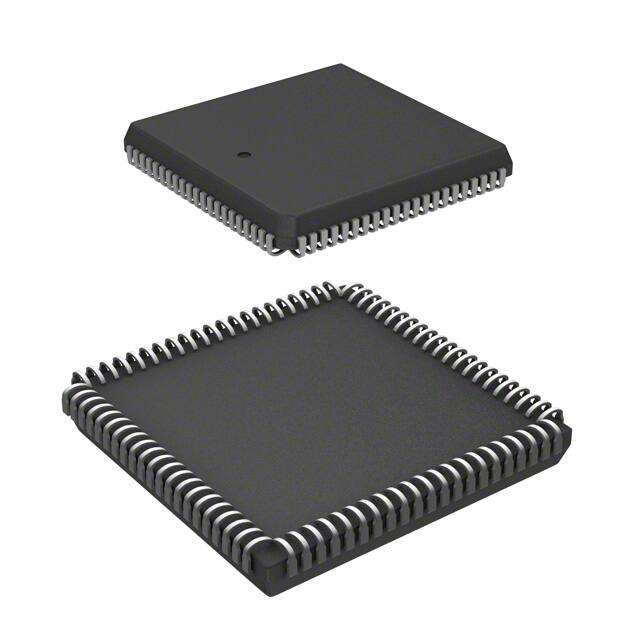


 工商网监
湘ICP备2023018690号
工商网监
湘ICP备2023018690号
