LT1121/LT1121-3.3/LT1121-5
Micropower Low Dropout
Regulators with Shutdown
FEATURES
DESCRIPTION
0.4V Dropout Voltage
n 150mA Output Current
n 30µA Quiescent Current
n No Protection Diodes Needed
n Adjustable Output from 3.75V to 30V
n 3.3V and 5V Fixed Output Voltages
n Controlled Quiescent Current in Dropout
n Shutdown
n 16µA Quiescent Current in Shutdown
n Stable with 0.33µF Output Capacitor
n Reverse Battery Protection
n No Reverse Current with Input Low
n Thermal Limiting
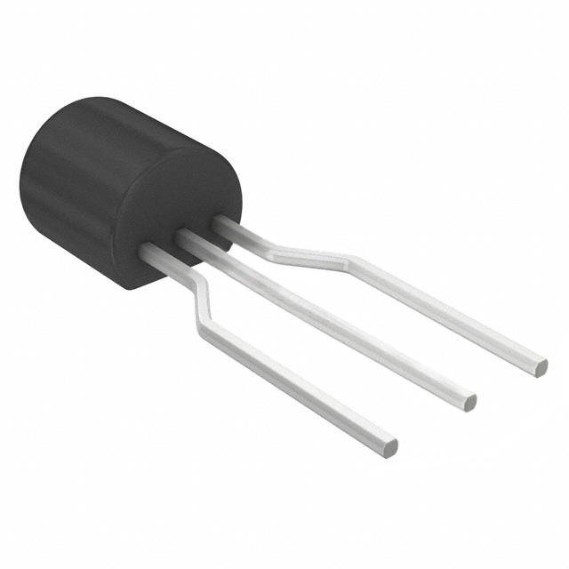
n Available in the 8-Lead SO, 8-Lead PDIP, 3-Lead
SOT-23 and 3-Lead TO-92 Packages
The LT®1121/LT1121-3.3/LT1121-5 are micropower low
dropout regulators with shutdown. These devices are capable of supplying 150mA of output current with a dropout
voltage of 0.4V. Designed for use in battery-powered systems, the low quiescent current, 30µA operating and 16µA
in shutdown, makes them an ideal choice. The quiescent
current is well-controlled; it does not rise in dropout as it
does with many other low dropout PNP regulators.
n
APPLICATIONS
Low Current Regulator
Regulator for Battery-Powered Systems
n Post Regulator for Switching Supplies
n
n
Other features of the LT1121/LT1121-3.3/LT1121-5 include
the ability to operate with very small output capacitors.
They are stable with only 0.33µF on the output while most
older devices require between 1µF and 100µF for stability.
Small ceramic capacitors can be used, enhancing manufacturability. Also the input may be connected to ground
or a reverse voltage without reverse current flow from
output to input. This makes the LT1121 series ideal for
backup power situations where the output is held high and
the input is at ground or reversed. Under these conditions
only 16µA will flow from the output pin to ground.
L, LT, LTC, LTM, Linear Technology and the Linear logo are registered trademarks of Linear
Technology Corporation. All other trademarks are the property of their respective owners.
TYPICAL APPLICATION
5V Battery-Powered Supply with Shutdown
Dropout Voltage
0.5
IN
OUT
1
LT1121-3.3
5V
5
+
SHDN
GND
3
VSHDN (PIN 5) OUTPUT
2.8
ON
NC
ON
3.3VOUT
150mA
1μF
SOLID TANTALUM
0.4
DROPOUT VOLTAGE (V)
8
0.3
0.2
0.1
LT1121 • TA01
0
0
20
40 60 80 100 120 140 160
OUTPUT CURRENT (mA)
LT1121 • TA02
1121fg
1
�LT1121/LT1121-3.3/LT1121-5
ABSOLUTE MAXIMUM RATINGS
(Note 1)
Input Voltage
LT1121............................................................... ± 30V
LT1121HV................................................ +36V, – 30V
Output Pin Reverse Current .................................. 10mA
Adjust Pin Current ................................................. 10mA
Shutdown Pin Input Voltage (Note 2)........... 6.5V, – 0.6V
Shutdown Pin Input Current (Note 2) ................... 20mA
Output Short-Circuit Duration ........................ Indefinite
Operating Junction Temperature Range (Note 3)
LT1121C-X............................................. 0°C to 125°C
LT1121I-X ......................................... – 40°C to 125°C
Storage Temperature Range...................– 65°C to 150°C
Lead Temperature (Soldering, 10 sec).................... 300°C
PIN CONFIGURATION
TOP VIEW
OUT 1
8 IN
NC/ADJ* 2
7 NC**
GND 3
6 NC**
NC 4
5 SHDN
N8 PACKAGE
8-LEAD PDIP
S8 PACKAGE
8-LEAD PLASTIC SO
* PIN 2 = NC FOR LT1121-3.3/LT1121-5
= ADJ FOR LT1121
** PINS 6 AND 7 ARE FLOATING (NO
INTERNAL CONNECTION) ON THE
STANDARD S8 PACKAGE.
PINS 6 AND 7 CONNECTED TO GROUND
ON THE A VERSION OF THE LT1121 (S8 ONLY).
CONNECTING PINS 6 AND 7 TO THE
GROUND PLANE WILL REDUCE THERMAL
RESISTANCE. SEE THERMAL RESISTANCE
TABLES IN THE APPLICATIONS INFORMATION
SECTION.
TJMAX = 150°C, θJA = 120°C/W (N8, S8)
TJMAX = 150°C, θJA = 70°C/W (AS8)
BOTTOM VIEW
FRONT VIEW
TAB IS
GND
3
OUTPUT
2
GND
1
VIN
IN
GND
OUT
ST PACKAGE
3-LEAD PLASTIC SOT-223
Z PACKAGE
3-LEAD PLASTIC TO-92
TJMAX = 150°C, θJA = 50°C/W
TJMAX = 150°C, θJA = 150°C/W
ORDER INFORMATION
LEAD FREE FINISH
TAPE AND REEL
PART MARKING
PACKAGE DESCRIPTION
TEMPERATURE RANGE
LT1121CN8#PBF
LT1121CN8#TRPBF
LT1121CN8
8-Lead Plastic PDIP
0°C to 125°C
LT1121CN8-3.3#PBF
LT1121CN8-3.3#TRPBF
LT1121CN8-3.3
8-Lead Plastic PDIP
0°C to 125°C
LT1121CN8-5#PBF
LT1121CN8-5#TRPBF
LT1121CN8-5
8-Lead Plastic PDIP
0°C to 125°C
LT1121IN8#PBF
LT1121IN8#TRPBF
LT1121IN8
8-Lead Plastic PDIP
–40°C to 125°C
LT1121IN8-3.3#PBF
LT1121IN8-3.3#TRPBF
LT1121IN8-3.3
8-Lead Plastic PDIP
–40°C to 125°C
LT1121IN8-5#PBF
LT1121IN8-5#TRPBF
LT1121IN8-5
8-Lead Plastic PDIP
–40°C to 125°C
LT1121CS8#PBF
LT1121CS8#TRPBF
1121
8-Lead Plastic S0
0°C to 125°C
LT1121CS8-3.3#PBF
LT1121CS8-3.3#TRPBF
11213
8-Lead Plastic S0
0°C to 125°C
LT1121CS8-5#PBF
LT1121CS8-5#TRPBF
11215
8-Lead Plastic S0
0°C to 125°C
LT1121HVCS8#PBF
LT1121HVCS8#TRPBF
1121HV
8-Lead Plastic S0
–40°C to 125°C
LT1121IS8#PBF
LT1121IS8#TRPBF
1121I
8-Lead Plastic S0
–40°C to 125°C
LT1121IS8-3.3#PBF
LT1121IS8-3.3#TRPBF
121I3
8-Lead Plastic S0
–40°C to 125°C
LT1121IS8-5#PBF
LT1121IS8-5#TRPBF
121I5
8-Lead Plastic S0
–40°C to 125°C
LT1121HVIS8#PBF
LT1121HVIS8#TRPBF
121HVI
8-Lead Plastic S0
–40°C to 125°C
LT1121ACS8#PBF
LT1121ACS8#TRPBF
1121A
8-Lead Plastic S0
0°C to 125°C
LT1121ACS8-3.3#PBF
LT1121ACS8-3.3#TRPBF
1121A3
8-Lead Plastic S0
0°C to 125°C
LT1121ACS8-5#PBF
LT1121ACS8-5#TRPBF
1121A5
8-Lead Plastic S0
0°C to 125°C
1121fg
2
�LT1121/LT1121-3.3/LT1121-5
ORDER INFORMATION
LEAD FREE FINISH
TAPE AND REEL
PART MARKING
PACKAGE DESCRIPTION
TEMPERATURE RANGE
LT1121AHVCS8#PBF
LT1121AHVCS8#TRPBF
121AHV
8-Lead Plastic S0
0°C to 125°C
LT1121AIS8#PBF
LT1121AIS8#TRPBF
121AI
8-Lead Plastic S0
–40°C to 125°C
LT1121AIS8-3.3#PBF
LT1121AIS8-3.3#TRPBF
121AI3
8-Lead Plastic S0
–40°C to 125°C
LT1121AIS8-5#PBF
LT1121AIS8-5#TRPBF
121AI5
8-Lead Plastic S0
–40°C to 125°C
LT1121AHVIS8#PBF
LT1121AHVIS8#TRPBF
21AHVI
8-Lead Plastic S0
–40°C to 125°C
LT1121CST-3.3#PBF
LT1121CST-3.3#TRPBF
11213
3-Lead Plastic SOT-223
0°C to 125°C
LT1121IST-3.3#PBF
LT1121IST-3.3#TRPBF
121I3
3-Lead Plastic SOT-223
–40°C to 125°C
LT1121CST-5#PBF
LT1121CST-5#TRPBF
11215
3-Lead Plastic SOT-223
0°C to 125°C
LT1121IST-5#PBF
LT1121IST-5#TRPBF
1121I5
3-Lead Plastic SOT-223
–40°C to 125°C
LT1121CZ3-3#PBF
LT1121CZ3-3#TRPBF
LT1121CZ3-3
3-Lead Plastic TO-92
0°C to 125°C
LT1121IZ3-3#PBF
LT1121IZ3-3#TRPBF
LT1121IZ3-3
3-Lead Plastic TO-92
–40°C to 125°C
LT1121CZ-5#PBF
LT1121CZ-5#TRPBF
LT1121CZ-5
3-Lead Plastic TO-92
0°C to 125°C
LT1121IZ-5#PBF
LT1121IZ-5#TRPBF
LT1121IZ-5
3-Lead Plastic TO-92
–40°C to 125°C
Consult LTC Marketing for parts specified with wider operating temperature ranges. *The temperature grade is identified by a label on the shipping container.
Consult LTC Marketing for information on nonstandard lead based finish parts.
For more information on lead free part marking, go to: http://www.linear.com/leadfree/
For more information on tape and reel specifications, go to: http://www.linear.com/tapeandreel/
ELECTRICAL
CHARACTERISTICS
The l denotes the specifications which apply over the full operating
temperature range, otherwise specifications are at TA = 25°C.
PARAMETER
CONDITIONS
Regulated Output Voltage (Note 4)
LT1121-3.3
LT1121-5
LT1121 (Note 5)
Line Regulation
Load Regulation
Dropout Voltage (Note 6)
MIN
TYP
MAX
UNITS
VIN = 3.8V, IOUT = 1mA, TJ = 25ºC
4.3V < VIN < 20V, 1mA < IOUT < 150mA
l
3.25
3.2
3.3
3.3
3.35
3.4
V
V
VIN = 5.5V, IOUT = 1mA, TJ = 25ºC
6V < VIN < 20V, 1mA < IOUT < 150mA
l
4.925
4.85
5
5
5.075
5.15
V
V
VIN = 4.3V, IOUT = 1mA, TJ = 25ºC
4.8V < VIN < 20V, 1mA < IOUT < 150mA
l
3.695
3.64
3.75
3.75
3.805
3.86
V
V
1.5
1.5
1.5
10
10
10
mV
mV
mV
–12
–20
–17
–28
–12
–18
–25
–40
–35
–50
–25
–40
mV
mV
mV
mV
mV
mV
0.13
0.16
0.25
V
V
0.3
0.35
0.5
V
V
0.37
0.45
0.6
V
V
0.42
0.55
0.7
V
V
LT1121-3.3
ΔVIN = 4.8V TO 20V, IOUT = 1mA
LT1121-5
ΔVIN = 5.5V TO 20V, IOUT = 1mA
LT1121 (Note 5) ΔVIN = 4.3V TO 20V, IOUT = 1mA
LT1121-3.3
ΔILOAD = 1mA to 150mA, TJ = 25ºC
ΔILOAD = 1mA to 150mA
LT1121-5
ΔILOAD = 1mA to 150mA, TJ = 25ºC
ΔILOAD = 1mA to 150mA
LT1121 (Note 5) ΔILOAD = 1mA to 150mA, TJ = 25ºC
ΔILOAD = 1mA to 150mA
l
l
l
l
l
l
ILOAD = 1mA, TJ = 25ºC
ILOAD = 1mA
l
ILOAD = 50mA, TJ = 25ºC
ILOAD = 50mA
l
ILOAD = 100mA, TJ = 25ºC
ILOAD = 100mA
l
ILOAD = 150mA, TJ = 25ºC
ILOAD = 150mA
l
1121fg
3
�LT1121/LT1121-3.3/LT1121-5
ELECTRICAL
CHARACTERISTICS
The l denotes the specifications which apply over the full operating
temperature range, otherwise specifications are at TA = 25°C.
PARAMETER
CONDITIONS
MIN
Ground Pin Current (Note 7)
ILOAD = 0mA
ILOAD = 1mA
ILOAD = 10mA
ILOAD = 50mA
ILOAD = 100mA
ILOAD = 150mA
Adjust Pin Bias Current (Notes 5, 8)
TJ = 25ºC
Shutdown Threshold
VOUT = Off to On
VOUT = On to Off
l
l
Shutdown Pin Current (Note 9)
VSHDN = 0V
l
l
l
l
l
l
l
Quiescent Current in Shutdown (Note 10) VIN = 6V, VSHDN = 0V
l
Ripple Rejection
VIN – VOUT = 1V (Avg), VRIPPLE = 0.5VP-P , fRIPPLE = 120Hz,
ILOAD = 0.1A
Current Limit
VIN – VOUT = 7V, TJ = 25ºC
Input Reverse Leakage Current
VIN = –20V, VOUT = 0V
Reverse Output Current (Note 11)
LT1121-3.3
VOUT = 3.3V, VIN = 0V
LT1121-5
VOUT = 5V, VIN = 0V
LT1121 (Note 5) VOUT = 3.8V, VIN = 0V
Note 1: Stresses beyond those listed under Absolute Maximum Ratings
may cause permanent damage to the device. Exposure to any Absolute
Maximum Rating condition for extended periods may affect device
reliability and lifetime.
Note 2: The shutdown pin input voltage rating is required for a low
impedance source. Internal protection devices connected to the shutdown
pin will turn on and clamp the pin to approximately 7V or – 0.6V. This
range allows the use of 5V logic devices to drive the pin directly. For high
impedance sources or logic running on supply voltages greater than 5.5V,
the maximum current driven into the shutdown pin must be limited to less
than 20mA.
Note 3: For junction temperatures greater than 110°C, a minimum load
of 1mA is recommended. For TJ > 110°C and IOUT < 1mA, output voltage
may increase by 1%.
Note 4: Operating conditions are limited by maximum junction
temperature. The regulated output voltage specification will not apply
for all possible combinations of input voltage and output current. When
operating at maximum input voltage, the output current range must be
limited. When operating at maximum output current the input voltage
range must be limited.
0.25
50
TYP
MAX
UNITS
30
90
350
1.5
4
7
50
120
500
2.5
7
14
µA
µA
µA
mA
mA
mA
150
300
nA
1.2
0.75
2.8
V
V
6
10
µA
16
22
58
200
l
16
16
16
µA
dB
500
mA
1
mA
25
25
25
µA
µA
µA
Note 5: The LT1121 (adjustable version) is tested and specified with the
adjust pin connected to the output pin.
Note 6: Dropout voltage is the minimum input/output voltage required to
maintain regulation at the specified output current. In dropout the output
voltage will be equal to: (VIN – VDROPOUT).
Note 7: Ground pin current is tested with VIN = VOUT (nominal) and a
current source load. This means that the device is tested while operating in
its dropout region. This is the worst case ground pin current. The ground
pin current will decrease slightly at higher input voltages.
Note 8: Adjust pin bias current flows into the adjust pin.
Note 9: Shutdown pin current at VSHDN = 0V flows out of the shutdown pin.
Note 10: Quiescent current in shutdown is equal to the sum total of the
shutdown pin current (6µA) and the ground pin current (9µA).
Note 11: Reverse output current is tested with the input pin grounded and
the output pin forced to the rated output voltage. This current flows into
the output pin and out of the ground pin.
1121fg
4
�LT1121/LT1121-3.3/LT1121-5
TYPICAL PERFORMANCE CHARACTERISTICS
Dropout Voltage
0.6
0.6
TJ ≤ 125°C
0.5
0.4
TJ ≤ 25°C
0.3
0.2
0.1
0
Quiescent Current
50
ILOAD = 150mA
ILOAD = 100mA
0.5
0.4
0.3
ILOAD = 50mA
0.2
ILOAD = 1mA
0.1
= TEST POINTS
0
0
–50
40 60 80 100 120 140 160
OUTPUT CURRENT (mA)
20
50
25
0
75
TEMPERATURE (°C)
–25
100
1121 G01
VSHDN = OPEN
40
2
3 4 5 6 7
INPUT VOLTAGE (V)
80
VSHDN = OPEN
60
40
20
VSHDN = 0V
1
8
9
0
10
1
0
2
3.32
3.30
3.28
3.26
3.24
3 4 5 6 7
INPUT VOLTAGE (V)
8
9
50
0
75
25
TEMPERATURE (°C)
80
VSHDN = OPEN
60
40
0
10
100
125
1121 G07
VSHDN = 0V
1
0
2
3 4 5 6 7
INPUT VOLTAGE (V)
9
10
1121 G06
3.83
IOUT = 1mA
5.06
3.81
5.04
3.79
5.02
5.00
4.98
4.96
4.92
–50
8
LT1121
Adjust Pin Voltage
IOUT = 1mA
3.77
3.75
3.73
3.71
3.69
4.94
–25
125
100
TJ = 25°C
RLOAD = ∞
VOUT = VADJ
20
ADJ PIN VOLTAGE (V)
OUTPUT VOLTAGE (V)
OUTPUT VOLTAGE (V)
5.08
3.34
50
25
0
75
TEMPERATURE (°C)
–25
100
LT1121-5
Output Voltage
IOUT = 1mA
3.22
–50
10
1121 G05
LT1121-3.3
Output Voltage
3.36
VSHDN = 0V
120
VSHDN = 0V
1121 G04
3.38
20
1121 G03
QUIESCENT CURRENT (μA)
80
0
30
0
–50
125
TJ = 25°C
RLOAD = ∞
100
QUIESCENT CURRENT (μA)
QUIESCENT CURRENT (μA)
100
20
VSHDN = OPEN
LT1121
Quiescent Current
120
TJ = 25°C
RLOAD = ∞
60
40
LT1121-5
Quiescent Current
120
VIN = 6V
RLOAD = ∞
1121 G02
LT1121-3.3
Quiescent Current
0
QUIESCENT CURRENT (μA)
0.7
DROPOUT VOLTAGE (V)
DROPOUT VOLTAGE (V)
Guaranteed Dropout Voltage
0.7
–25
50
0
75
25
TEMPERATURE (°C)
100
125
1121 G08
3.67
–50
–25
50
0
75
25
TEMPERATURE (°C)
100
125
1121 G09
1121fg
5
�LT1121/LT1121-3.3/LT1121-5
TYPICAL PERFORMANCE CHARACTERISTICS
800
TJ = 25°C
RLOAD = 130Ω
ILOAD = 25mA*
600
500
RLOAD = 330Ω
ILOAD = 10mA*
400
300
*FOR VOUT = 3.3V
200
RLOAD = 3.3k
ILOAD = 1mA*
100
0
0
1
2
3 4 5 6 7
INPUT VOLTAGE (V)
8
9
800
RLOAD = 200Ω
ILOAD = 25mA*
600
500
RLOAD = 500Ω
ILOAD = 10mA*
400
300
*FOR VOUT = 5V
200
RLOAD = 5k
ILOAD = 1mA*
100
0
10
2
1
0
3 4 5 6 7
INPUT VOLTAGE (V)
8
1121 G10
10
RLOAD = 22Ω
ILOAD = 150mA*
7
6
RLOAD = 33Ω
ILOAD = 100mA*
5
4
3
RLOAD = 66Ω
ILOAD = 50mA*
2
1
0
1
2
3 4 5 6 7
INPUT VOLTAGE (V)
8
9
RLOAD = 33Ω
ILOAD = 150mA*
6
RLOAD = 50Ω
ILOAD = 100mA*
5
4
3
RLOAD = 100Ω
ILOAD = 50mA*
2
1.8
2
0
0
2
1
3 4 5 6 7
INPUT VOLTAGE (V)
8
9
20
40 60 80 100 120 140 160
OUTPUT CURRENT (mA)
1121 G16
3 4 5 6 7
INPUT VOLTAGE (V)
8
10
RLOAD = 25Ω
ILOAD = 150mA*
7
6
5
RLOAD = 38Ω
ILOAD = 100mA*
4
3
RLOAD = 75Ω
ILOAD = 50mA*
2
*FOR VOUT = 3.75V
0
1
2
3 4 5 6 7
INPUT VOLTAGE (V)
8
10
9
1121 G15
Shutdown Pin Threshold
(Off-to-On)
2.0
ILOAD = 1mA
1.8
1.6
1.4
1.2
1.0
0.8
0.6
0.4
0
–50
9
8
0
10
1.6
ILOAD = 150mA
1.4
1.2
ILOAD = 1mA
1.0
0.8
0.6
0.4
0.2
0.2
0
2
1
*FOR VOUT = 5V
SHUTDOWN THRESHOLD (V)
4
SHUTDOWN THRESHOLD (V)
GROUND PIN CURRENT (mA)
2.0
TJ = –55°C
1
1121 G12
Shutdown Pin Threshold
(On-to-Off)
TJ = 25°C
0
1121 G14
14
6
RLOAD = 3.8k
ILOAD = 1mA*
TJ = 25°C
9 VOUT = VADJ
7
Ground Pin Current
TJ = 125°C
*FOR VOUT = 3.75V
200
LT1121
Ground Pin Current
1121 G13
8
300
0
10
8
0
10
VIN = 3.3V (LT1121-3.3)
VIN = 5V (LT1121-5)
12 V = 3.75V (LT1121)
IN
DEVICE IS OPERATING
10 IN DROPOUT
RLOAD = 380Ω
ILOAD = 10mA*
400
10
1
*FOR VOUT = 3.3V
0
500
100
TJ = 25°C
9
GROUND PIN CURRENT (mA)
GROUND PIN CURRENT (mA)
8
600
LT1121-5
Ground Pin Current
TJ = 25°C
9
9
RLOAD = 150Ω
ILOAD = 25mA*
1121 G11
LT1121-3.3
Ground Pin Current
10
TJ = 25°C
700 VOUT = VADJ
TJ = 25°C
700
GROUND PIN CURRENT (μA)
GROUND PIN CURRENT (μA)
700
LT1121
Ground Pin Current
GROUND PIN CURRENT (mA)
800
LT1121-5
Ground Pin Current
GROUND PIN CURRENT (μA)
LT1121-3.3
Ground Pin Current
–25
50
25
0
75
TEMPERATURE (°C)
100
125
1121 G17
0
–50
–25
50
25
0
75
TEMPERATURE (°C)
100
125
1121 G18
1121fg
6
�LT1121/LT1121-3.3/LT1121-5
TYPICAL PERFORMANCE CHARACTERISTICS
Shutdown Pin Current
SHUTDOWN PIN INPUT CURRENT (mA)
SHUTDOWN PIN CURRENT (μA)
8
7
6
5
4
3
2
1
0
–50
50
25
0
75
TEMPERATURE (°C)
–25
400
25
VSHDN = 0V
9
100
20
15
10
5
0
125
ADJUST PIN BIAS CURRENT (nA)
10
LT1121
Adjust Pin Bias Current
Shutdown Pin Input Current
7
3
8
2
5
6
4
SHUTDOWN PIN VOLTAGE (V)
1
0
1121 G19
Reverse Output Current
15
10
5
100
VOUT = 0V
300
300
250
200
150
100
50
0
1
4
2
5
3
INPUT VOLTAGE (V)
0
0
1
2
3 4 5 6 7 8
OUTPUT VOLTAGE (V)
200
150
100
0
–50
7
6
9
10
1121 G25
–25
50
0
75
25
TEMPERATURE (°C)
100
1121 G24
Ripple Rejection
IOUT = 100mA
90 VIN = 6V + 50mVRMS RIPPLE
RIPPLE REJECTION (dB)
80
60
58
56
54
50
–50
125
100
COUT = 47μF
SOLID TANTALUM
70
60
50
40
30
COUT = 1μF
SOLID TANTALUM
20
52
LT1121-5
10
125
250
1121 G23
RIPPLE REJECTION (dB)
OUTPUT PIN CURRENT (μA)
20
100
50
VIN = VOUT (NOMINAL) + 1V
+ 0.5VP-P RIPPLE AT f = 120Hz
62
IOUT = 100mA
LT1121-3.3
50
0
75
25
TEMPERATURE (°C)
Current Limit
Ripple Rejection
LT1121
(VOUT = VADJ)
–25
1121 G21
64
TJ = 25°C
90 VIN = 0V
CURRENT FLOWS
80 INTO OUTPUT PIN
70
30
50
VIN = 7V
350 VOUT = 0V
Reverse Output Current
40
100
350
0
125
100
50
150
400
1121 G22
60
200
0
–50
9
CURRENT LIMIT (mA)
SHORT-CIRCUIT CURRENT (mA)
OUTPUT PIN CURRENT (μA)
20
50
25
0
75
TEMPERATURE (°C)
250
Current Limit
400
VIN = 0V
VOUT = 5V (LT1121-5)
25 VOUT = 3.3V (LT1121-3.3)
VOUT = 3.8V (LT1121)
–25
300
1121 G20
30
0
–50
350
10
–25
50
25
0
75
TEMPERATURE (°C)
100
125
1121 G26
0
10
100
1k
10k
FREQUENCY (Hz)
100k
1M
1121 G27
1121fg
7
�LT1121/LT1121-3.3/LT1121-5
TYPICAL PERFORMANCE CHARACTERISTICS
LT1121-5
Load Transient Response
Load Regulation
ΔILOAD = 1mA TO 150mA
OUTPUT VOLTAGE
DEVIATION (V)
LT1121*
–10
LT1121-3.3
–15
–20
VIN = 6V
0.2 CIN = 0.1μF
= 1μF
C
0.1 OUT
0
–0.1
–0.2
VIN = 6V
0.2 CIN = 0.1μF
COUT = 3.3μF
0.1
0
–0.1
–0.2
LT1121-5
–30
–35
* ADJ PIN TIED TO
OUTPUT PIN
–40
–50
–25
50
0
75
25
TEMPERATURE (°C)
100
125
150
100
0 0.1 0.2 0.3 0.4 0.5 0.6 0.7 0.8 0.9 1.0
TIME (ms)
1121 G28
1121 G29
LOAD CURRENT
(mA)
–25
LOAD CURRENT
(mA)
LOAD REGULATION (mV)
–5
OUTPUT VOLTAGE
DEVIATION (V)
0
LT1121-5
Load Transient Response
150
100
50
0 0.1 0.2 0.3 0.4 0.5 0.6 0.7 0.8 0.9 1.0
TIME (ms)
1121 G30
PIN FUNCTIONS
Input Pin: Power is supplied to the device through the
input pin. The input pin should be bypassed to ground if
the device is more than six inches away from the main
input filter capacitor. In general the output impedance of
a battery rises with frequency so it is usually adviseable to
include a bypass capacitor in battery-powered circuits. A
bypass capacitor in the range of 0.1µF to 1µF is sufficient.
The LT1121 is designed to withstand reverse voltages on
the input pin with respect to both ground and the output
pin. In the case of a reversed input, which can happen if
a battery is plugged in backwards, the LT1121 will act as
if there is a diode in series with its input. There will be
no reverse current flow into the LT1121 and no reverse
voltage will appear at the load. The device will protect both
itself and the load.
Output Pin: The output pin supplies power to the load. An
output capacitor is required to prevent oscillations. See
the Applications Information section for recommended
value of output capacitance and information on reverse
output characteristics.
Shutdown Pin: This pin is used to put the device into
shutdown. In shutdown the output of the device is turned
off. This pin is active low. The device will be shut down if
the shutdown pin is pulled low. The shutdown pin current
with the pin pulled to ground will be 6µA. The shutdown
pin is internally clamped to 7V and – 0.6V (one VBE). This
allows the shutdown pin to be driven directly by 5V logic or
by open collector logic with a pull-up resistor. The pull-up
resistor is only required to supply the leakage current of
the open collector gate, normally several microamperes.
Pull-up current must be limited to a maximum of 20mA.
A curve of shutdown pin input current as a function of
voltage appears in the Typical Performance Characteristics.
If the shutdown pin is not used it can be left open circuit.
The device will be active, output on, if the shutdown pin
is not connected.
Adjust Pin: For the adjustable LT1121, the adjust pin
is the input to the error amplifier. This pin is internally
clamped to 6V and –0.6V (one VBE). It has a bias current
of 150nA which flows into the pin. See Bias Current curve
in the Typical Performance Characteristics. The adjust
pin reference voltage is 3.75V referenced to ground. The
output voltage range that can be produced by this device
is 3.75V to 30V.
1121fg
8
�LT1121/LT1121-3.3/LT1121-5
APPLICATIONS INFORMATION
The LT1121 is a micropower low dropout regulator with
shutdown, capable of supplying up to 150mA of output
current at a dropout voltage of 0.4V. The device operates
with very low quiescent current (30µA). In shutdown the
quiescent current drops to only 16µA. In addition to the
low quiescent current the LT1121 incorporates several
protection features which make it ideal for use in batterypowered systems. The device is protected against both
reverse input voltages and reverse output voltages. In
battery backup applications where the output can be held
up by a backup battery when the input is pulled to ground,
the LT1121 acts like it has a diode in series with its output
and prevents reverse current flow.
approximately 15ppm/°C. The adjust pin bias current has
a negative temperature coefficient. These effects are small
and will tend to cancel each other.
Adjustable Operation
Thermal Considerations
The adjustable version of the LT1121 has an output voltage
range of 3.75V to 30V. The output voltage is set by the
ratio of two external resistors as shown in Figure 1. The
device servos the output voltage to maintain the voltage
at the adjust pin at 3.75V. The current in R1 is then equal
to 3.75V/R1. The current in R2 is equal to the sum of the
current in R1 and the adjust pin bias current. The adjust
pin bias current, 150nA at 25°C, flows through R2 into the
adjust pin. The output voltage can be calculated according
to the formula in Figure 1. The value of R1 should be less
than 400k to minimize errors in the output voltage caused
by the adjust pin bias current. Note that in shutdown the
output is turned off and the divider current will be zero.
Curves of Adjust Pin Voltage vs Temperature and Adjust
Pin Bias Current vs Temperature appear in the Typical
Performance Characteristics. The reference voltage at the
adjust pin has a slight positive temperature coefficient of
Power handling capability will be limited by maximum
rated junction temperature (125°C). Power dissipated by
the device will be made up of two components:
IN
VOUT
OUT
LT1121
R2
SHDN
ADJ
+
R1
GND
1121 • F01
(
)
VOUT = 3.75V 1 + R2 + IADJ • R2
R1
VADJ = 3.75V
IADJ = 150nA AT 25°C
OUTPUT RANGE = 3.75V TO 30V
(
)
Figure 1. Adjustable Operation
The adjustable device is specified with the adjust pin tied
to the output pin. This sets the output voltage to 3.75V.
Specifications for output voltage greater than 3.75V will
be proportional to the ratio of the desired output voltage
to 3.75V (VOUT/3.75V). For example: load regulation for an
output current change of 1mA to 150mA is –12mV typical
at VOUT = 3.75V. At VOUT = 12V, load regulation would be:
⎛ 12V ⎞
⎜⎝ 3.75V ⎟⎠ • ( –12mV ) = ( –38mV )
1. Output current multiplied by the input/output voltage
differential: IOUT • (VIN – VOUT), and
2. Ground pin current multiplied by the input voltage:
IGND • VIN.
The ground pin current can be found by examining the
Ground Pin Current curves in the Typical Performance
Characteristics. Power dissipation will be equal to the
sum of the two components listed above.
The LT1121 series regulators have internal thermal limiting
designed to protect the device during overload conditions.
For continuous normal load conditions the maximum junction temperature rating of 125°C must not be exceeded.
It is important to give careful consideration to all sources
of thermal resistance from junction to ambient. Additional
heat sources mounted nearby must also be considered.
Heat sinking, for surface mount devices, is accomplished
by using the heat spreading capabilities of the PC board
and its copper traces. Copper board stiffeners and plated
through holes can also be used to spread the heat generated by power devices. Tables 1 through 5 list thermal
resistances for each package. Measured values of thermal
resistance for several different board sizes and copper
areas are listed for each package. All measurements were
taken in still air, on 3/32" FR-4 board with 1oz copper. All
1121fg
9
�LT1121/LT1121-3.3/LT1121-5
APPLICATIONS INFORMATION
NC leads were connected to the ground plane.
Table 1. N8 Package*
COPPER AREA
Table 5. TO-92 Package THERMAL RESISTANCE
Package alone
220ºC/W
Package soldered into PC board with plated through
holes only
175ºC/W
Package soldered into PC board with 1/4 sq. inch of
copper trace per lead
145ºC/W
160ºC/W
135ºC/W
BOARD AREA
THERMAL RESISTANCE
JUNCTION TO AMBIENT
2500 sq mm 2500 sq mm
2500 sq mm
80ºC/W
1000 sq mm 2500 sq mm
2500 sq mm
80ºC/W
Package soldered into PC board with plated through
holes in board, no extra copper trace, and a clip-on type
heat sink: Thermalloy type 2224B
225 sq mm
2500 sq mm
2500 sq mm
85ºC/W
Aavid type 5754
1000 sq mm 1000 sq mm
1000 sq mm
91ºC/W
TOPSIDE
BACKSIDE
* Device is mounted on topside. Leads are through hole and are
soldered to both sides of board.
Table 2. S8 Package
COPPER AREA
BOARD AREA
THERMAL RESISTANCE
JUNCTION TO AMBIENT
2500 sq mm 2500 sq mm
2500 sq mm
120ºC/W
1000 sq mm 2500 sq mm
2500 sq mm
120ºC/W
225 sq mm
2500 sq mm
2500 sq mm
125ºC/W
100 sq mm
1000 sq mm
1000 sq mm
131ºC/W
TOPSIDE*
BACKSIDE
* Device is mounted on topside.
Table 3. AS8 Package*
COPPER AREA
BOARD AREA
THERMAL RESISTANCE
JUNCTION TO AMBIENT
2500 sq mm 2500 sq mm
2500 sq mm
60ºC/W
1000 sq mm 2500 sq mm
2500 sq mm
60ºC/W
225 sq mm
2500 sq mm
2500 sq mm
68ºC/W
100 sq mm
2500 sq mm
2500 sq mm
74ºC/W
TOPSIDE**
BACKSIDE
* Pins 3, 6 and 7 are ground.
** Device is mounted on topside.
BOARD AREA
THERMAL RESISTANCE
JUNCTION TO AMBIENT
2500 sq mm 2500 sq mm
2500 sq mm
50ºC/W
1000 sq mm 2500 sq mm
2500 sq mm
50ºC/W
225 sq mm
2500 sq mm
2500 sq mm
58ºC/W
100 sq mm
2500 sq mm
2500 sq mm
64ºC/W
1000 sq mm 2500 sq mm
1000 sq mm
57ºC/W
1000 sq mm
1000 sq mm
60ºC/W
TOPSIDE*
BACKSIDE
0
* Tab of device attached to topside copper.
Example: given an output voltage of 3.3V, an input voltage
range of 4.5V to 7V, an output current range of 0mA to
100mA, and a maximum ambient temperature of 50°C,
what will the maximum junction temperature be?
Power dissipated by the device will be equal to:
IOUT MAX • (VIN MAX – VOUT) + (IGND • VIN)
where, IOUT MAX = 100mA
VIN MAX = 7V
IGND at (IOUT = 100mA, VIN = 7V) = 5mA
so,
P = 100mA • (7V – 3.3V) + (5mA • 7V)
= 0.405W
If we use an SOT-223 package, then the thermal resistance
will be in the range of 50°C/W to 65°C/W depending on
copper area. So the junction temperature rise above ambient will be less than or equal to:
0.405W • 60°C/W = 24°C
The maximum junction temperature will then be equal to
the maximum junction temperature rise above ambient
plus the maximum ambient temperature or:
Table 4. SOT-223 Package
(Thermal Resistance Junction-to-Tab 20ºC/W)
COPPER AREA
Calculating Junction Temperature
TJMAX = 50°C + 24°C = 74°C
Output Capacitance and Transient Performance
The LT1121 is designed to be stable with a wide range of
output capacitors. The minimum recommended value is 1µF
with an ESR of 3Ω or less. For applications where space
is very limited, capacitors as low as 0.33µF can be used if
combined with a small series resistor. Assuming that the
ESR of the capacitor is low (ceramic) the suggested series
1121fg
10
�LT1121/LT1121-3.3/LT1121-5
APPLICATIONS INFORMATION
Table 6. Suggested Series Resistor Values
OUTPUT CAPACITANCE
SUGGESTED SERIES RESISTOR
0.33µF
2Ω
0.47µF
1Ω
0.68µF
1Ω
>1µF
None Needed
Protection Features
The LT1121 incorporates several protection features
which make it ideal for use in battery-powered circuits.
In addition to the normal protection features associated
with monolithic regulators, such as current limiting and
thermal limiting, the device is protected against reverse
input voltages, reverse output voltages, and reverse voltages from output to input.
Current limit protection and thermal overload protection
are intended to protect the device against current overload
conditions at the output of the device. For normal operation, the junction temperature should not exceed 125°C.
The input of the device will withstand reverse voltages of
30V. Current flow into the device will be limited to less
than 1mA (typically less than 100µA) and no negative
voltage will appear at the output. The device will protect
both itself and the load. This provides protection against
batteries that can be plugged in backwards.
For fixed voltage versions of the device, the output can
be pulled below ground without damaging the device. If
the input is open circuit or grounded the output can be
pulled below ground by 20V. The output will act like an
open circuit, no current will flow out of the pin. If the input
is powered by a voltage source, the output will source the
short-circuit current of the device and will protect itself by
thermal limiting. For the adjustable version of the device,
the output pin is internally clamped at one diode drop
below ground. Reverse current for the adjustable device
must be limited to 5mA.
In circuits where a backup battery is required, several
different input/output conditions can occur. The output
voltage may be held up while the input is either pulled
to ground, pulled to some intermediate voltage, or is left
open circuit. Current flow back into the output will vary
depending on the conditions. Many battery-powered circuits incorporate some form of power management. The
following information will help optimize battery life. Table
7 summarizes the following information.
The reverse output current will follow the curve in Figure
2 when the input pin is pulled to ground. This current
flows through the output pin to ground. The state of the
shutdown pin will have no effect on output current when
the input pin is pulled to ground.
In some applications it may be necessary to leave the
input to the LT1121 unconnected when the output is held
high. This can happen when the LT1121 is powered from
a rectified AC source. If the AC source is removed, then
the input of the LT1121 is effectively left floating. The
reverse output current also follows the curve in Figure 2
if the input pin is left open. The state of the shutdown pin
will have no effect on the reverse output current when the
input pin is floating.
100
OUTPUT PIN CURRENT (μA)
resistor is shown in Table 6. The LT1121 is a micropower
device and output transient response will be a function of
output capacitance. See the Transient Response curves
in the Typical Performance Characteristics. Larger values
of output capacitance will decrease the peak deviations
and provide improved output transient response. Bypass
capacitors, used to decouple individual components
powered by the LT1121, will increase the effective value
of the output capacitor.
TJ = 25°C
90 VIN < VOUT
CURRENT FLOWS
80
INTO OUTPUT PIN
70 TO GROUND
LT1121
(VOUT = VADJ)
60
50
40
LT1121-3.3
30
20
LT1121-5
10
0
0
1
2
3 4 5 6 7 8
OUTPUT VOLTAGE (V)
9
10
1121• F02
Figure 2. Reverse Output Current
1121fg
11
�LT1121/LT1121-3.3/LT1121-5
APPLICATIONS INFORMATION
5
VOUT = 3.3V (LT1121-3.3)
VOUT = 5V (LT1121-5)
4
INPUT CURRENT (μA)
When the input of the LT1121 is forced to a voltage below
its nominal output voltage and its output is held high, the
reverse output current will still follow the curve in Figure
2. This condition can occur if the input of the LT1121 is
connected to a discharged (low voltage) battery and the
output is held up by either a backup battery or by a second
regulator circuit. When the input pin is forced below the
output pin or the output pin is pulled above the input pin,
the input current will typically drop to less than 2µA (see
Figure 3). The state of the shutdown pin will have no effect
on the reverse output current when the output is pulled
above the input.
3
2
1
0
1
0
3
2
INPUT VOLTAGE (V)
4
5
1121 F03
Figure 3. Input Current
Table 7. Fault Conditions
INPUT PIN
SHDN PIN
OUTPUT PIN


 工商网监
湘ICP备2023018690号
工商网监
湘ICP备2023018690号
