LT3966
I2C Programmable Quad
Monolithic Boost LED Driver
FEATURES
DESCRIPTION
Four Independent DC/DC Channels
n I2C Programmable
n 8192:1 True Color PWM™ Dimming
n 8-Bit Analog Dimming Pin Scaled by DAC
n 11-Channel, 8-Bit ADC with 2 External Inputs
n 1.6A, 60V Internal DMOS Switches
n Input Voltage: 3V to 60V
n Output Voltage and Current Monitoring to 60V
n High Side PMOS Disconnect and PWM Switch Driver
n Adjustable Frequency: 300kHz to 4MHz with Optional
Frequency Synchronization
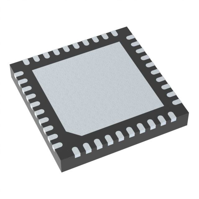
n Thermally Enhanced 6mm × 6mm 40-Lead QFN Package
n AEC-Q100 Qualification in Progress
The LT®3966 is an I2C programmable monolithic boost
LED driver with four independent channels. Each channel provides a 60V current mode boost converter with
an internal 1.6A DMOS power switch, as well as internal and external analog and PWM dimming features. I2C
programmable features include a 13-bit (8192:1) digital
PWM generator, 8-bit analog dimming DAC, and flexible
fault reporting and handling.
An onboard 8-bit ADC allows measurement of each
channel’s output voltage and output current, as well
as chip input voltage and two external measurements.
In addition, independent shutdown and standby control of each channel provides flexible solutions for
multitopology applications.
The LT3966 is available in a thermally enhanced 6mm ×
6mm 40-Lead QFN package.
n
APPLICATIONS
n
n
Backlighting
Heads Up Displays
All registered trademarks and trademarks are the property of their respective owners.
TYPICAL APPLICATION
100W Buck Mode LED Driver with I2C Dimming
4.7μF
×4
ISP1
ISP2
ISP3
ISP4
330mΩ
330mΩ
330mΩ
330mΩ
ISN1
ISN2
ISN3
ISN4
TG1
1μF
TG2
TG3
1μF
68μH
VIN SW1
1μF
TG4
68μH
SW3
1MΩ
68μH
GND
CTRL/
EXT2 PWM1–4 SDA SCL ALERT
I2C
BUS
85
80
70
0.0
fSW = 360kHz
VIN = 48V
VOUT = 34V
0.5
1.0
1.5
2.0
LED CURRENT (A)
(4 × 750mA/4 CH)
TG1–4
EXT1
90
75
SW4
ISN1–4
LT3966
INTVCC
95
ISP1–4
EN/UVLO
33k
100
1μF
68μH
SW2
Efficiency
EFFICIENCY (%)
VIN
44V TO 52V
2.5
3.0
3966 TA01b
FB1–4
RT
SYNC ADR1–2 INTVCC
150k
360kHz
MULTIPHASE
3966 TA01a
97.6k
4.7μF
22.1k
Rev. 0
Document Feedback
For more information www.analog.com
1
�LT3966
ABSOLUTE MAXIMUM RATINGS
PIN CONFIGURATION
(Note 1)
ISN2
FB2
RT
SYNC
EXT2
EN/UVLO
INTVCC
VIN
FB1
TOP VIEW
ISN1
VIN, EN/UVLO, SW1, SW2, SW3, SW4, ISP1, ISP2,
ISP3, ISP4, ISN1, ISN2, ISN3, ISN4.......................62V
ISP–ISN (Any Channel)................................................2V
TG1–4................................................................. (Note 2)
INTVCC................................................................ (Note 3)
FB1–4, EXT1–2, CTRL/PWM1–4, ADR1–2, ALERT,
SDA, SCL, SYNC...................................................5.5V
RT................................................................................2V
Operating Junction Temperature Range (Notes 4, 5)
LT3966E............................................. –40°C to 125°C
LT3966J............................................. –40°C to 150°C
Storage Temperature Range................... –65°C to 150°C
40 39 38 37 36 35 34 33 32 31
ISP1 1
30 ISP2
TG1 2
29 TG2
SW1 3
28 SW2
SW1 4
27 SW2
SW3 5
26 SW4
41
GND
SW3 6
25 SW4
TG3 7
24 TG4
ISP3 8
23 ISP4
ISN3 9
22 ISN4
FB3 10
21 FB4
ALERT
SCL
SDA
ADR2
EXT1
ADR1
CTRL/PWM4
CTRL/PWM3
CTRL/PWM2
CTRL/PWM1
11 12 13 14 15 16 17 18 19 20
QFN PACKAGE
40-LEAD (6mm × 6mm) PLASTIC QFN
TJMAX = 150°C, θJA = 33°C/W EXPOSED PAD (PIN 41) IS GND
AND MUST BE SOLDERED TO PCB
ORDER INFORMATION
LEAD FREE FINISH
TAPE AND REEL
PART MARKING
PACKAGE DESCRIPTION
TEMPERATURE RANGE
LT3966EUJ#PBF
LT3966EUJ#TRPBF
LT3966UJ
40-Lead (6mm × 6mm) Plastic QFN
–40°C to 125°C
LT3966JUJ#PBF
LT3966JUJ#TRPBF
LT3966UJ
40-Lead (6mm × 6mm) Plastic QFN
–40°C to 150°C
Contact the factory for parts specified with wider operating temperature ranges. *The temperature grade is identified by a label on the shipping container.
Tape and reel specifications. Some packages are available in 500 unit reels through designated sales channels with #TRMPBF suffix.
ELECTRICAL CHARACTERISTICS
The l denotes specifications that apply over the full operating temperature
range, otherwise specifications are at TA = 25°C. VIN = 12V unless otherwise noted.
PARAMETER
CONDITIONS
VIN Operating Range
MIN
l
TYP
3
MAX
UNITS
60
V
VIN Quiescent Current
CTRL/PWM = 0V, EN/UVLO = 1.3V
2.7
3.3
mA
VIN Shutdown Current
EN/UVLO = 0V
EN/UVLO = 1.15V, CTRL/PWM = 0V
0
190
1
230
µA
µA
1.23
1.26
V
EN/UVLO Shutdown Threshold Falling
l
EN/UVLO Rising Hysteresis
EN/UVLO Rising
EN/UVLO Input Low Voltage
IVIN < 1μA
1.20
15
mV
0.4
V
Rev. 0
2
For more information www.analog.com
�LT3966
ELECTRICAL CHARACTERISTICS
The l denotes specifications that apply over the full operating temperature
range, otherwise specifications are at TA = 25°C. VIN = 12V unless otherwise noted.
PARAMETER
CONDITIONS
MIN
TYP
MAX
UNITS
EN/UVLO Bias Current Low
EN/UVLO = 1.15V
2
EN/UVLO Bias Current High
EN/UVLO = 1.3V
10
100
nA
3
3.1
V
µA
LDO Regulator
INTVCC Regulation Voltage
IINTVCC = –1mA, Not Switching
INTVCC Line Regulation
3V ≤ VIN ≤ 60V
INTVCC Load Regulation
–20mA ≤ IINTVCC ≤ 0mA, Not Switching
INTVCC Undervoltage Lockout
INTVCC Falling
l
2.9
0.03
%/V
0.04
l
2.6
2.7
%/mA
2.8
V
INTVCC Undervoltage Lockout Hysteresis
INTVCC Rising
75
mV
INTVCC Current Limit
VIN = 12V, INTVCC = 2.8V
36
mA
INTVCC Dropout Voltage
VIN = 3V, IINTVCC = –15mA
320
mV
8
Bits
Analog-to-Digital Converter
Converter Resolution
Converter Full-Scale Voltage
1.266
Converter LSB Size
4.95
Conversion Time (tCONV)
Rt = 100kΩ, MPHASE = 0, AUTO = 0
EXT1, EXT2 Input Impedance
VEXT1 = VEXT2 = 1V
EXT1, EXT2 Internal Voltage Clamp
IEXT1 = IEXT2 = 100μA
1.275
1.284
V
5
5.05
mV
20
l
10
100
1.4
1.7
EXT1, EXT2 Internal Voltage Clamp Impedance VEXT1 = VEXT2 = 2V to 5.5V
µs
MΩ
1.9
2.2
V
kΩ
Channel 1–4 LED Current Sense Amplifiers
ISP Common Mode Voltage Range
l
3
55
V
Full-Scale Current Sense Threshold
(VISP–VISN)
ISP = 55V, CTRL/PWM =1.5V, ADIM[7:0] = 0xFF
ISP = 3V, CTRL/PWM = 1.5V, ADIM[7:0] = 0xFF
l
l
242
242
250
250
255
255
mV
mV
Externally Adjusted Half-Scale Threshold
(VISP–VISN)
ISP = 55V, CTRL/PWM = 0.7V, ADIM[7:0] = 0xFF l
ISP = 3V, CTRL/PWM = 0.7V, ADIM[7:0] = 0xFF l
122
122
125
125
128
128
mV
mV
Externally Adjusted 1/10th Scale Threshold
(VISP–VISN)
ISP = 55V, CTRL/PWM = 0.3V, ADIM[7:0] = 0xFF l
ISP = 3V, CTRL/PWM = 0.3V, ADIM[7:0] = 0xFF l
20
20
25
25
31
31
mV
mV
Internally Adjusted Half-Scale Threshold
(VISP–VISN)
ISP = 55V, CTRL/PWM = 1.5V, ADIM[7:0] =
0x7F
ISP = 3V, CTRL/PWM = 1.5V, ADIM[7:0] = 0x7F
l
l
121
121
125
125
129
129
mV
mV
Internally Adjusted 1/10th Scale Threshold
(VISP–VISN)
ISP = 55V, CTRL/PWM = 1.5V, ADIM[7:0] =
0x19
ISP = 3V, CTRL/PWM = 1.5V, ADIM[7:0] = 0x19
l
l
20
20
25
25
31
31
mV
mV
Overcurrent Protection Threshold (VISP–VISN)
ISP = 60V
C/10 Threshold
ISP = 60V
ISP/ISN Input Bias Current (Combined)
CTRL/PWM = 3V (Active), ISP = ISN = 55V
CTRL/PWM = 0V (Standby), ISP = ISN = 55V
PWM Threshold
CTRL/PWM Falling
370
14
l
90
mV
22
30
mV
440
13
17
µA
µA
103
115
mV
Rev. 0
For more information www.analog.com
3
�LT3966
ELECTRICAL CHARACTERISTICS
The l denotes specifications that apply over the full operating temperature
range, otherwise specifications are at TA = 25°C. VIN = 12V unless otherwise noted.
PARAMETER
CONDITIONS
MIN
ISP Voltage Regulation Threshold
TYP
MAX
62
UNITS
V
Channel 1–4 Voltage Feedback Amplifiers
FB Regulation Threshold (VFB)
CTRL/PWM = 2V
l
FB Overvoltage Threshold
FB Open LED Threshold
FB Shorted LED Threshold
l
FB Input Bias Current
Current Out of Pin, FB = 1V
FB Line Regulation
3.3V ≤ VIN ≤ 60V
1.188
1.170
1.200
1.200
1.208
1.218
V
V
VFB + 50mV
VFB + 60mV
VFB + 70mV
V
VFB – 40mV
VFB – 50mV
VFB – 60mV
280
300
320
mV
10
100
nA
0.0004
V
%/V
Oscillator
RT Pin Voltage
1.0
V
Switching Frequency in Single-Phase Mode
RT = 261kΩ
RT = 100kΩ
RT = 47.5kΩ
l
l
l
370
0.93
1.85
400
1.00
2.00
430
1.07
2.15
kHz
MHz
MHz
Switching Frequency in Multiphase Mode
RT = 174kΩ
RT = 47.5kΩ
RT = 21kΩ
l
l
l
279
0.93
1.85
300
1.00
2.00
321
1.07
2.15
kHz
MHz
MHz
Minimum Off Time
30
50
65
ns
Minimum On Time
35
60
75
ns
SYNC Input High (SYNC In Mode)
SYNCOUT = 0
SYNC Input Low (SYNC In Mode)
SYNCOUT = 0
1.5
SYNC Input Duty Cycle
V
10
SYNC Resistance to GND (SYNC In Mode)
SYNCOUT = 0
SYNC Output Mode Duty Cycle
SYNCOUT = 1
SYNC Output Voltage High (SYNC Out Mode)
SYNCOUT = 1, Load = 3kΩ
l
SYNC Output Voltage Low (SYNC Out Mode)
SYNCOUT = 1, Load = 3kΩ
l
0.4
V
90
%
95
45
55
kΩ
65
2.4
%
V
0.4
V
Channel 1–4 Power Switch
SW On-Resistance
ISW = 200mA
SW Current Limit
SW Leakage Current
200
l
1.6
2
mΩ
2.4
A
3
μA
8.2
9
V
0.3
V
VSW = 62V
External PMOS Gate Driver
TG ON Voltage (VISP–VTG)
ISP = 24V
7.4
TG OFF Voltage (VISP–VTG)
ISP = 24V
0
TG Turn-On Time
CLOAD = 470pF, ISP = 24V
50
ns
TG Turn-Off Time
CLOAD = 470pF, ISP = 24V
60
ns
I2C Port
I2C Address
Programmed by ADR2, ADR1 Pins
101XXXX[R/W]
ADR1, ADR2 Input High Voltage
l
ADR1, ADR2 Input Low Voltage
l
ADR1, ADR2 Pull-Down Current in HIGH State
VADR1, VADR2 = 3V, Current Into Pin
l
ADR1, ADR2 Pull-Up Current in LOW State
VADR1, VADR2 = 0V, Current Out of Pin
0.9 • VINTVCC
V
0.1 • VINTVCC
V
9
13
17
µA
13
17
µA
l
9
SDA, SCL Input High Voltage
l
1.5
SDA ,SCL Input Low Voltage
l
V
0.4
V
Rev. 0
4
For more information www.analog.com
�LT3966
ELECTRICAL CHARACTERISTICS
The l denotes specifications that apply over the full operating temperature
range, otherwise specifications are at TA = 25°C. VIN = 12V unless otherwise noted.
PARAMETER
CONDITIONS
MIN
TYP
SDA, SCL Input Low Leakage
Current Out of Pin, SDA = SCL = 0V
50
nA
SDA, SCL Input High Leakage
Current Into Pin, SDA = SCL = 3V
50
nA
SDA Output Low Voltage
ISDA = 3mA
0.4
V
ALERT Output Low Voltage
IALERT = 3mA
I2C Clock Operating Frequency
MAX
UNITS
0.4
V
400
kHz
Bus Free Time Between Stop and Start
Condition (tBUF)
1.3
µs
Hold Time After Repeated Start Condition (tHD_SDA)
0.6
µs
Repeated Start Condition Set-Up Time (tSU_STA)
0.6
µs
Stop Condition Set-Up Time (tSU_STO)
0.6
µs
Data Hold Time Output (tHD_DAT(O))
0
Data Hold Time Input (tHD_DAT(I))
0
ns
100
ns
Data Set-Up Time (tSU_DAT)
900
ns
SCL Clock Low Period (tLOW)
1.3
µs
SCL Clock High Period (tHIGH)
0.6
µs
Clock/Data Fall Time
CB = Capacitance of One Bus Line (pF)
20 + 0.1CB
300
Clock/Data Rise Time
CB = Capacitance of One Bus Line (pF)
20 + 0.1CB
300
ns
50
ns
125
ms
Input Spike Suppression Pulse Width (tSP)
Watchdog Timeout Period
WDTEN = 1
75
Note 1: Stresses beyond those listed under Absolute Maximum Ratings
may cause permanent damage to the device. Exposure to any Absolute
Maximum Rating condition for extended periods may affect device
reliability and lifetime.
Note 2: Do not apply a positive or negative voltage source to TG pins,
otherwise permanent damage may occur.
Note 3: Do not apply a positive or negative voltage source to INTVCC pin,
otherwise permanent damage may occur. IINTVCC = 2mA is the maximum
external load that can be applied.
Note 4: The LT3966E is guaranteed to meet performance specifications
from the 0°C to 125°C junction temperature. Specifications over the
–40°C to 125°C operating junction temperature range are assured by
100
ns
design, characterization and correlation with statistical process controls.
The LT3966J is guaranteed to meet performance specifications over the
full –40°C to 150°C operating junction temperature range. High junction
temperatures degrade operating lifetimes. Operating lifetime is derated at
junction temperatures greater than 125°C.
Note 5: The LT3966 includes overtemperature protection that is intended
to protect the device during momentary overload conditions. Junction
temperature will exceed the maximum operating junction temperature
when overtemperature is active. Continuous operating above the specified
maximum operating junction temperature may impair device reliability.
Note 6: Guaranteed by a combination of design, testing, and
characterization over the operating temperature range, and automated
testing at ambient temperature.
SDA
tSU,DAT
tHD,DATO
tHD,DATI
tSU,STA
tSP
tHD,STA
tSP
tBUF
tSU,STO
3966 TD
SCL
tHD,STA
REPEATED START
CONDITION
REPEATED START
CONDITION
STOP
CONDITION
START
CONDITION
Rev. 0
For more information www.analog.com
5
�LT3966
TYPICAL PERFORMANCE CHARACTERISTICS
Shutdown and Standby Current
Shutdown and Standby Current
vs Input
Voltage
vs
Input Voltage
1.30
250
STANDBY
EN/UVLO = 0V
EN/UVLO = 1.15V
100
150
EN/UVLO = 0V
EN/UVLO = 1.15V
100
50
SHUTDOWN
0
10
20
30
VIN (V)
40
50
0
–50 –25
60
1.24
0
1.20
–50 –25
25 50 75 100 125 150
TEMPERATURE (°C)
EN/UVLO = 1.15V
2.4
INTV
INTVcc
CC Voltage vs Input Voltage
3.2
EN/UVLO = 2V, CTRL/PWM1 –4 = 0V,
FB1-4 = 1.3V
3.2
3.1
3.0
INTVCC (V)
VIN IQ (mA)
3.0
2.8
2.6
1.8
0
2.2
25 50 75 100 125 150
TEMPERATURE (°C)
0
10
20
30
VIN (V)
40
50
2.5
60
40
3.08
INTVCC DROPOUT (mV)
IINTVCC (mA)
36
34
32
0
25 50 75 100 125 150
TEMPERATURE (°C)
30
–50 –25
40
50
60
500
400
300
200
100
2.92
2.90
–50 –25
30
VIN (V)
600
VIN = 12V
INTVCC = 2.8V
2.96
2.94
20
INTVCC Dropout vs
Temperature
3.04
2.98
10
3966 G06
38
3.06
IINTVCC = –15mA
0
3966 G05
INTVCC Current Limit
vs Temperature
INTV
vs
Temperature
CC Voltage vs Temperature
3.00
2.8
2.6
3966 G04
3.02
2.9
2.7
2.4
1.6
1.4
–50 –25
25 50 75 100 125 150
TEMPERATURE (°C)
3966 G03
Quiescent Current vs Input Voltage
2.0
0
3966 G02
3.4
2.2
RISING THRESHOLD
FALLING THRESHOLD
SHUTDOWN
3966 G01
2.6
INTVCC (V)
1.26
1.22
50
EN/UVLO Hysteresis Current
vs Temperature
3.10
1.28
VEN/UVLO (V)
150
IEN/UVLO (µA)
STANDBY
200
VIN CURRENT (µA)
VIN CURRENT (µA)
200
2.8
EN/UVLO Thresholds
vs Temperature
vs Temperature
vs Temperature
vs
Temperature
250
0
TA = 25°C, unless otherwise noted.
0
25 50 75 100 125 150
TEMPERATURE (°C)
3966 G08
3966 G07
0
–50 –25
IINTVCC = –15mA
0
25 50 75 100 125 150
TEMPERATURE (°C)
3966 G09
Rev. 0
6
For more information www.analog.com
�LT3966
TYPICAL PERFORMANCE CHARACTERISTICS
INTVCC Dropout vs
Temperature
Load
vs Load
Switching Frequency
Switching
Frequency vs RT
vs
RT
10
400
TA = 25°C, unless otherwise noted.
vs Temperature
1060
250
200
150
100
SWITCHING FREQUENCY (kHz)
SWITCHING FREQUENCY (MHz)
INTVCC DROPOUT (mV)
300
1
1020
1000
0
3
6
9
IINTVCC (mA)
12
0.1
15
100
RT (kΩ)
3966 G10
VFB
FB vs Temperature
ISP VOLTAGE LIMIT (V)
1.19
1.18
25 50 75 100 125 150
TEMPERATURE (°C)
3966 G12
260
63
1.20
0
3966 G11
VISP–ISN vs Temperature
ISP = 48V
258
1.21
256
254
62
61
252
250
248
246
60
244
1.17
242
1.16
–50 –25
0
59
–50 –25
25 50 75 100 125 150
TEMPERATURE (°C)
0
240
–50 –25
25 50 75 100 125 150
TEMPERATURE (°C)
390
275
ISP = 48V
252
380
200
375
175
370
365
248
360
247
355
246
350
–50 –25
0
6
12 18 24 30 36 42 48 54 60
VISP (V)
ISP = 48V
225
VISP–ISN (mV)
VISP–ISN OCP (mV)
385
249
VISP–ISN vs ADIM
VCTRL/PWM
CTRL/PWM
250
253
250
25 50 75 100 125 150
TEMPERATURE (°C)
3966 G15
VISP–ISN Threshold vs
Temperature
Protection
Threshold vsOvercurrent
Temperature
VISP–ISN vs VISP
251
0
3966 G14
3966 G13
VISP–ISN (mV)
940
ISP Voltage Limit vs Temperature
1.22
254
960
900
–50 –25
1k
64
1.23
VFB (V)
10
VISP–ISN (mV)
1.24
980
920
50
0
RT = 100k
1040
350
150
125
100
75
50
25
0
25 50 75 100 125 150
TEMPERATURE (°C)
3966 G17
3966 G16
0
0
0.2 0.4 0.6 0.8 1 1.2 1.4 1.6 1.8 2.0
VCTRL/PWM (V)
3966 G18
Rev. 0
For more information www.analog.com
7
�LT3966
TYPICAL PERFORMANCE CHARACTERISTICS
VISP–ISN vs ADIM VFB
275
ISP = 48V
225
VISP–ISN (mV)
VISP–ISN (mV)
125
100
75
ILED MEASURED CODE
200
150
175
150
125
100
75
50
50
25
25
0
32
64
400
192
160
128
96
64
32
0
0
0.255
0.510
0.765
VFB (V)
1.020
1.12
1.14
3966 G20
TG RISE/FALL TIME (ns)
2.2
1.8
10 20 30 40 50 60 70 80 90 100
DUTY CYCLE (%)
3966 G25
32 64 96 128 160 192 224 256 288 320
VISP–ISN (mV)
3966 G21
Switch Current Limit
vs Temperature
250
200
150
100
50
0
2.2
2.1
2.0
1.9
1.8
1.7
–50 –25
25 50 75 100 125 150
TEMPERATURE (°C)
0
25 50 75 100 125 150
TEMPERATURE (°C)
Minimum On/Off Time
vs Temperature
80
RISE
FALL
ISP = 24V
100
80
60
40
0
3966 G24
TG Rise/Fall
Time vs CLOAD
LOAD
20
0
0
2.3
120
1.9
0
1.22
300
140
2.0
64
3966 G23
2.3
SWITCH CURRENT LIMIT (A)
1.20
350
Switch Current Limit
vs
vs Duty
Duty Cycle
Cycle
1.7
1.16 1.18
VFB (V)
3966 G22
2.1
96
Switch On-Resistance
vs Temperature
0
–50 –25
1.275
128
SWITCH CURRENT LIMIT (A)
SWITCH ON–RESISTANCE (mΩ)
FB MEASURED CODE
224
160
32
3966 G19
FB Measured Code vs VFB
ISP = 48V
192
ISP = 48V
0
1.10
96 128 160 192 224 256
ADIM CODE
ILED
Measured Code vs VISP–ISN
ISP–ISN
224
225
175
256
256
250
200
0
VISP–ISN vs VFB
MINIMUM ON/OFF TIME (ns)
250
TA = 25°C, unless otherwise noted.
0
200
400
600
CLOAD (pF)
800
1000
3966 G26
MINIMUM ON
MINIMUM OFF
70
60
50
40
30
–50 –25
0
25 50 75 100 125 150
TEMPERATURE (°C)
3966 G27
Rev. 0
8
For more information www.analog.com
�LT3966
PIN FUNCTIONS
FB1, FB2, FB3, FB4 (Pins 39, 32, 10, 21): Voltage
Feedback Pin. The FB pin is used for output voltage regulation and limiting. Tie to a resistor divider from the output
voltage. When FB reaches 1.2V, the switch current will
reduce in order to maintain the output voltage at this level.
If ISP/ISN senses less than 10% of full output current
when FB reaches regulation, an OPENLED condition will
be flagged for that channel. If FB is driven above 1.26V,
the external PMOS will be switched off and an OVFB condition will be flagged. If FB remains below 0.3V after the
internal soft start has completed, a SHORTLED condition
will be flagged. See the Applications Information section
for more information on faults and fault handling.
ADR1, ADR2, (Pins 16, 17): I2C Address Select. These
pins are configured as three-state inputs (HIGH, LOW,
FLOAT). See Table 1 for address selection.
ISP1, ISP2, ISP3, ISP4 (Pins 1, 30, 8, 23): Positive
Terminal of the LED Current Sense Amplifier. Also serves
as the positive supply of the TG gate driver. Connect to
positive side of LED current sense resistor and minimize
resistance in this path.
SYNC (Pin 34): Oscillator Synchronization Pin. By default,
this pin acts as an input for an external clock to define
the switching frequency of the LT3966. By setting the
SYNCOUT configuration bit, the input function is disabled
and instead SYNC becomes a clock output for driving
other external circuits.
ISN1, ISN2, ISN3, ISN4 (Pins 40, 31, 9, 22): Negative
Terminal of the LED Current Sense Amplifier. Kelvin connects to negative side of LED current sense resistor.
TG1, TG2, TG3, TG4 (Pins 2, 29, 7, 24): Top Gate Driver
Output. Connect to gate of external PMOS pass transistor.
TG is an inverted and level-shifted version of the PWM
dimming signal, and drives between VISP (OFF) and VISP–
8.2V (ON) for LED PWM dimming as well as fault mode
disconnect. Leave unconnected if not used.
SW1, SW2, SW3, SW4 (Pins 3–4, 27–28, 5–6, 25–26):
Power DMOS Drain. Connect to switching end of the
inductor. Minimize copper area to increase efficiency and
reduce EMI.
CTRL/PWM1, CTRL/PWM2, CTRL/PWM3, CTRL/PWM4
(Pins 11, 12, 13, 14): Combination Analog/PWM Dimming
Input. Drive from below 100mV to above 1.5V for fullscale PWM dimming. Or drive with an analog voltage from
0.2V to 1.2V for 0% to 100% analog dimming. Do not
leave these pins floating, tie to INTVCC if unused.
EXT1, EXT2 (Pins 15, 35): External Input to ADC. The
working range of the EXT input is 0V (Code 0) to 1.275V
(Code 255). These pins are internally clamped to 1.7V.
Tie to GND if unused.
ALERT (Pin 20): Chip Status Reporting Pin. Depending
on channel configuration, the ALERT pin can be pulled
low due to any of the following faults: FB Overvoltage,
Open LED, Shorted LED, and LED Overcurrent. See the
Applications Information section for more information on
faults and fault handling.
SDA (Pin 18): Serial Data Line for I2C Communications.
Combination input and open-drain output.
SCL (Pin 19): Serial Clock for I2C Communications.
RT (Pin 33): Timing Resistor Set Pin. Set the master clock
frequency using a resistor to GND. Do not leave the RT
pin open.
EN/UVLO (Pin 36): Enable/Undervoltage Lockout Pin.
This pin is used for general ON/OFF control and to enable
the LT3966 at a specific input voltage. Drive with a logic
level greater than 1.5V for simple ON/OFF control, or tie to
a resistor divider of input voltage for precision shutdown
threshold. This pin has a falling threshold of 1.23V, rising
hysteresis of roughly 15mV, and a 2µA hysteresis current
when below threshold. Tie this pin to VIN if unused.
INTVCC (Pin 37): Internal 3V LDO Output. This pin is the
LDO output and power supply for all internal circuitry.
Place a 4.7μF filter capacitor to GND as close to this pin
as possible. Do not drive this pin externally. Users may
apply a load of up to 2mA to this pin.
VIN (Pin 38): Input Voltage Supply. This pin is the power
supply input to the LDO and the rest of the internal circuitry. It must be locally bypassed with a capacitor to GND
as close to the pin as possible.
Rev. 0
For more information www.analog.com
9
�LT3966
BLOCK DIAGRAM
RT
RT
SYNC
EN/UVLO
VIN
1.2V
BANDGAP
OSCILLATOR
I2C INTERFACE
AND
GLOBAL LOGIC
3V
VCCUV
ALERT
ADC
MUX
FB1–4
VLED1–4
OVFB1
FB1
+
×4
–
ISP1
RISP
1.2V
VLED1
50mV
–+
ISN1
CTRL/
PWM1
1.2V
0.1V
TG1
FAULT1
–
+
R1
IOUT
IREF
+
+
–
VC1
RUN1
OPENLED1
LEDOC1
CHANNEL
LOGIC & FAULT
SHORT1
HANDLING
TSD
VCCUV
SOFTSTART
DAC8
R1
×4
+
–
–
+
LATOFF
1.7V
SS1
ADIM1[7:0]
–
+
FB1
1.26V
+
FB1
–
1.15V
VLED1
0.1V
VLED1
1.5V
FB1
+
1.6A
–
+
–
PWM1
R
+
S
+
–
CURRENT
SENSOR
DATA
R/W
SLOPE COMP
SW1
Q
ADC8
–
CLK1
ALERT
VIN
EXT1
EXT2
EXT2
SDA
+
EXT1
SCL
SDA
–
1.08V
SCL
ACK/SDA0
CLK1–4
+
–
INTVCC
MCLK
+
INTVCC
ADR2
–
+
–
ADR1
FAULT1–4
+
–
ENUV
0.3V
SSDONE1
PWEXT1
ISP1
PWM1
ISP1 –8.2V
FAULT1
PWINT1
DIMMING
GENERATOR
DIMEN1
BAM1
SEL1[2:0]
DIM1[12:0]
CHANNEL DUPLICATED 4 TIMES
3966 BD
Rev. 0
10
For more information www.analog.com
�LT3966
OPERATION
OVERVIEW
The LT3966 is a 4-channel monolithic boost LED driver
with I2C programmability and onboard ADC. The 4 independent LED driver channels each consist of a 1.6A
monolithic boost converter with high side LED current
sensing and high side gate driver for PWM dimming and
fault protection. The analog LED current setpoint can be
controlled externally and also programmed through I2C.
The LED dimming can be controlled with an external PWM
signal or through I2C using the internal PWM generator.
Additionally, the LT3966 contains an 11-input, 8-bit ADC
used to measure regulation parameters of each of the LED
driver channels as well as input voltage, die temperature,
and two external inputs.
LT3966 operates from input voltages of 3V to 60V. The
1.23V EN threshold allows programmable external UVLO
using a resistor divider from the input voltage. All internal circuitry is powered from an onboard LDO regulator
supplying 3V at the INTVCC pin. Although the internal circuitry operates at 3V, all I/O pins are 5V tolerant. The LDO
is current limited to 36mA and should not be externally
loaded, and the device provides an internal UVLO to prevent switching when INTVCC falls below 2.7V. Bypass and
filtering of the LDO require a capacitor of at least 4.7μF
from INTVCC to GND located close to the pins.
The boost converters are internally compensated current
mode converters with a 1.6A power FET each. The boost
converters can operate from 300Hz to 4MHz, and switching can be synchronized to an external clock. Through I2C,
the LT3966 allows the options of multiphase switching for
lower input ripple as well as clock sync output.
The LED drivers use high side current sensing with a
250mV threshold. This analog threshold is externally
adjustable by using the CTRL/PWM pin, and is also internally programmable through I2C. A high side gate driver
for an external PMOS transistor allows accurate PWM
dimming, fast fault protection, and output disconnect.
PWM dimming can be controlled externally by toggling
CTRL/PWM, or internally programmed using the LT3966
onboard PWM generator. This PWM generator offers resolution from 6-bit (64:1) to 13-bit (8192:1), as well as the
choice between standard PWM modulation and optional
BAM (Bit Angle Modulation) control.
The LED drivers have detection and protection from
overvoltage, overcurrent, open LED, and shorted LED
conditions. Fault handling is autonomous, with optional
readback, fault reporting, and latchoff functions using I2C.
The device I2C address is programmable to one of eight
different addresses or standalone mode using the two trimode ADR pins. Reliable and robust I2C communication
is ensured by use of CRC error checking and an optional
watchdog timer.
I2C OPERATION
I2C Transactions and Error Correction Operation
I2C communication revolves around read and write transactions. In LT3966, Packet Error Checking (PEC) is used
to guarantee reliable communication between the host
system and the device. This consists of a trailing byte on
both the read and write transactions that offers a CRC
check of all bytes since the last start. The CRC polynomial used in LT3966 is identical to that used in SMBus:
X8 + X2 + X1 + 1.
The structure of an I2C write is shown in Figure 1. Data
being written to LT3966 must follow this format. The PEC
code (Figure 2) should be computed by the host system
using the CRC formula on the Chip Address, Sub Address,
and Data Bytes. If a valid PEC is received, the LT3966 will
acknowledge (ACK) on the 9th clock of the PEC transfer,
and the data will be transferred to the LT3966 register. If
an invalid PEC is received, the LT3966 will not ACK, and
the data will be discarded.
Rev. 0
For more information www.analog.com
11
�LT3966
OPERATION
SUB ADDRESS
DATA
PEC (CRC)
S7 S6 S5 S4 S3 S2 S1 S0
D7 D6 D5 D4 D3 D2 D1 D0
P7 P6 P5 P4 P3 P2 P1 P0
CHIP ADDRESS
1
0
1
SDA
1
0
1
SCL
1
2
3
A3 A2 A1 A0
0
START
STOP
0 ACK
4
5
6
7
8
9
ACK
1
2
3
4
5
6
7
8
9
ACK
1
2
3
4
5
6
7
8
9
ACK
1
2
3
4
5
6
7
8
9
3966 F01
Figure 1. I2C Write Transaction with PEC
// Bytewise CRC-8 for LT3966 using X8 + X2 + X + 1
// Takes a running sum (or 0) as , and current byte to CRC as
// Returns the CRC-8 of and for sending or further CRC’ing
int8_t doCRC(int8_t in, int8_t data){
int8_t crc;
int8_t i;
crc = in ^ data; // XOR the incoming bytes
for(i = 0; i < 8; i++){ // Step through each bit
if (crc & 0x80) { // If MSB is set
crc


 工商网监
湘ICP备2023018690号
工商网监
湘ICP备2023018690号
