Data Sheet
LTC2672
Five-Channel, Low Dropout, 300 mA, Current Source Output, 12-/16-Bit SoftSpan
DAC
FEATURES
►
►
►
►
►
►
►
►
►
►
►
►
►
FUNCTIONAL BLOCK DIAGRAM
Per channel programmable output current ranges: 300 mA,
200 mA, 100 mA, 50 mA, 25 mA, 12.5 mA, 6.25 mA, and
3.125 mA
Flexible 2.1 V to VCC output supply voltages
Flexible single- or dual-supply operation
0.6 V maximum dropout voltage guaranteed
Separate voltage supply per output channel
Internal switches to optional negative supply
Full 12-bit and 16-bit resolution at all ranges
Guaranteed operation −40°C to 125°C (H-grade)
Precision internal reference (10 ppm/°C maximum VREF
temperature coefficient) or external reference
Analog multiplexer monitors voltages and currents
A/B toggle via SPI or dedicated pin
1.71 V to VCC digital input and output supply voltage
32-lead lead frame chip scale package (LFCSP), see the
Outline Dimensions section
29
2
LTC2672
IOVCC
TGP
VDD0
DAC0
OUT0
3
4
5
6
7
31
SDI
SPAN0
SDO
SCK
VDD1
OUT1
23
SPAN1
CLR
V–
VDD2
GND
1, 8, 14, 32
OUT2
FAULT
DETECT
SPAN2
The LTC2672 is a family of five-channel, 12-/16-bit current source,
digital-to-analog converters (DACs) that provide five high compliance, current source outputs with guaranteed 0.6 V dropout at
200 mA. There are eight current ranges that are programmable
per channel with full-scale outputs of up to 300 mA. The channels
can be paralleled to allow either ultrafine adjustments of large
currents or combined outputs of up to 1.5 A. A dedicated supply
pin is provided for each output channel. Each channel can be
operated from 2.1 V to VCC, and internal switches allow any output
to be pulled to the optional negative supply. The LTC2672 includes
a precision integrated 1.25 V reference (10 ppm/°C maximum),
with the option to use an external reference. The serial peripheral
interface (SPI)-compatible, 3‑wire serial interface operates on logic
levels as low as 1.71 V and at clock rates as high as 50 MHz.
9
10
11
REFLO
DAC3
FULL SCALE
ADJUST
OUT3
REF
REFCOMP
SPAN3
INTERNAL
REFERENCE
MUX
V–
15, 26
19
V–
VDD4
VCC
13, 27
28
18
FSADJ
17
DAC4
OUT4
ANALOG
MUX
SPAN4
16
V–
001
GENERAL DESCRIPTION
12
20
V–
VDD3
Tunable lasers
► Semiconductor optical amplifier biasing
► Resistive heaters
► Current mode biasing
21
DAC2
APPLICATIONS
►
22
DAC1
LDAC
30
24
V–
SERIAL
INTERFACE
CS/LD
FAULT
25
Figure 1.
Note that throughout this data sheet, multifunction pins, such as
CS/LD, are referred to by the entire pin name or by a single function
of the pin.
Rev. A
DOCUMENT FEEDBACK
TECHNICAL SUPPORT
Information furnished by Analog Devices is believed to be accurate and reliable "as is". However, no responsibility is assumed by Analog
Devices for its use, nor for any infringements of patents or other rights of third parties that may result from its use. Specifications subject to
change without notice. No license is granted by implication or otherwise under any patent or patent rights of Analog Devices. Trademarks and
registered trademarks are the property of their respective owners.
�Data Sheet
LTC2672
TABLE OF CONTENTS
Features................................................................ 1
Applications........................................................... 1
General Description...............................................1
Functional Block Diagram......................................1
Specifications........................................................ 4
Timing Characteristics........................................7
Absolute Maximum Ratings...................................9
Thermal Resistance........................................... 9
ESD Caution.......................................................9
Pin Configuration and Function Descriptions...... 10
Typical Performance Characteristics................... 12
Terminology......................................................... 15
Theory of Operation.............................................16
Load Termination and Combining Channels.... 16
Power-On Reset...............................................16
Power Supply Sequencing............................... 16
Data Transfer Function.....................................16
Applications Information...................................... 17
Serial Interface................................................. 17
Input and DAC Registers..................................17
Output Ranges and SoftSpan Operation..........17
Monitor Multiplexer........................................... 20
Current Measurement Using the Multiplexer....20
Die Temperature Measurement Using the
Multiplexer...................................................... 20
Monitor Multiplexer Precharge
Considerations............................................... 20
Toggle Operations............................................ 21
Toggle Select Register (TSR)...........................21
Writing to Input Register A and Input
Register B.......................................................21
Toggling Between Register A and Register B.. 21
Daisy-Chain Operation..................................... 23
Echo Readback................................................ 23
Fault Register................................................... 23
Fault Indicator Pin (FAULT, Pin 30)..................23
Fault Conditions and Thermal Overload
Protection....................................................... 23
Configuration Command.................................. 23
Power-Down Mode...........................................24
Safe Supply Ranges.........................................24
Current Outputs................................................24
Switch to V− Mode............................................25
Gain Adjustment Using the FSADJ Pin............ 25
Offset Current and Code 0............................... 25
Reference Modes............................................. 25
Board Layout.................................................... 25
Outline Dimensions............................................. 26
Ordering Guide.................................................26
Evaluation Boards............................................ 27
REVISION HISTORY
4/2021—Rev. 0 to Rev. A
Added 12-Bit to Product Title........................................................................................................................... 1
Changes to Features Section.......................................................................................................................... 1
Changes to General Description Section.........................................................................................................1
Changes to Figure 1........................................................................................................................................ 1
Changes to Table 1.......................................................................................................................................... 4
Changes to Figure 2, Figure 3 Caption, and Figure 4 Caption........................................................................ 8
Changed UH-32 to 05-08-1693 in Table 5....................................................................................................... 9
Change to Figure 5........................................................................................................................................ 10
Added Figure 7 and Figure 11; Renumbered Sequentially............................................................................ 12
Changes to Integral Nonlinearity (INL) Section..............................................................................................15
Changes to Differential Nonlinearity (DNL) Section.......................................................................................15
Changes to Current Offset Error (IOS) Section............................................................................................. 15
Changes to Theory of Operation Section.......................................................................................................16
Changes to Load Termination and Combining Channels Section..................................................................16
Changes to Serial Interface Section.............................................................................................................. 17
Added Figure 23............................................................................................................................................ 17
Changes to Offset Current and Code 0 Section............................................................................................ 25
Updated Outline Dimensions......................................................................................................................... 26
Changes to Ordering Guide........................................................................................................................... 26
Added Evaluation Boards Section................................................................................................................. 27
analog.com
Rev. A | 2 of 27
�Data Sheet
LTC2672
REVISION HISTORY
12/2020—Revision 0: Initial Version
analog.com
Rev. A | 3 of 27
�Data Sheet
LTC2672
SPECIFICATIONS
All specifications apply over the full operating TJ range, unless otherwise noted. Typical values are at TJ = 25°C, VCC = IOVCC = 5 V, V− =
–3.3 V, VDDx = 5 V, FSADJ = VCC, and reference output voltage (VREF) = 1.25 V external, unless otherwise specified.
Table 1.
Parameter
Symbol
DC PERFORMANCE, LTC2672-16
Resolution
Monotonicity
Differential Nonlinearity
Integral Nonlinearity
Current Offset Error
IOS Temperature Coefficient
Gain Error
GE2
Gain Temperature Coefficient
Total Unadjusted Error
TUE2
Power Supply Rejection
PSR
DC Crosstalk3
Dropout Voltage (VDDx − VOUTx4)
Off Mode Output Leakage Current5
OUTx Switch to V− Resistance
DC PERFORMANCE, LTC2672-12
Resolution
Monotonicity
Differential Nonlinearity
Integral Nonlinearity
Current Offset Error
IOS Temperature Coefficient
Gain Error
All ranges1
DNL
INL
IOS
VDROPOUT
RPULLDOWN
DNL
INL
IOS
GE2
Gain Temperature Coefficient
Total Unadjusted Error
TUE2
Power Supply Rejection
PSR
DC Crosstalk3
analog.com
Test Conditions/Comments
All ranges1
All ranges1
All current ranges1
All current ranges
300 mA and 200 mA output current ranges
100 mA, 50 mA, and 25 mA output current ranges
12.5 mA, 6.25 mA, and 3.125 mA output current ranges
FSADJ = VCC
300 mA and 200 mA output current ranges
100 mA, 50 mA, and 25 mA output current ranges
12.5 mA, 6.25 mA, and 3.125 mA output current ranges
Range = 100 mA, OUTx current (IOUTx) = 50 mA
VCC = 4.75 V to 5.25 V
VDDx = 2.85 V to 3.15 V
VDDx = 4.75 V to 5.25 V
V− = −3.25 V to −2.75 V
Result of a 200 mW change in dissipated power
200 mA range, (VDDx − V−) = 4.75 V
200 mA range, (VDDx – V–) = 2.85 V
300 mA range, (VDDx – V–) = 4.75 V
300 mA range, (VDDx – V–) = 2.85 V
800 Ω load to GND
Span code = 1000b, sinking 80 mA
All ranges1
All ranges1
All ranges1
All current ranges1
All current ranges
300 mA and 200 mA output current ranges
100 mA, 50 mA, and 25 mA output current ranges
12.5 mA, 6.25 mA, and 3.125 mA output current ranges
FSADJ = VCC
300 mA and 200 mA output current ranges
100 mA, 50 mA, and 25 mA output current ranges
12.5 mA, 6.25 mA, and 3.125 mA output current ranges
Range = 100 mA, IOUTx = 50 mA
VCC = 4.75 V to 5.25 V
VDDx = 2.85 V to 3.15 V
VDDx = 4.75 V to 5.25 V
V− = −3.25 V to −2.75 V
Result of a 200 mW change in dissipated power
Min
16
16
−1
−64
−0.4
−0.9
−1.2
−1.5
−1.4
−1.7
−2
−1
12
12
−0.5
−4
−0.4
−0.9
−1.2
−1.5
−1.4
−1.7
−2
Typ
+0.45
+12
+0.1
10
+0.3
+0.4
+0.7
30
+0.4
+0.5
+0.8
0.5
0.4
0.7
0.6
0.1
0.45
0.5
0.75
0.85
+0.1
8
+0.03
+0.8
+0.1
10
+0.3
+0.4
+0.7
30
+0.4
+0.5
+0.8
0.04
0.03
0.05
0.04
0.1
Max
+1
+64
+0.4
+0.9
+1.2
+1.5
+1.4
+1.7
+2
0.6
0.65
1.15
+1
12
+0.5
+4
+0.4
+0.9
+1.2
+1.5
+1.4
+1.7
+2
Unit
Bits
Bits
LSB
LSB
%FSR
ppm/°C
%FSR
%FSR
%FSR
ppm/°C
%FSR
%FSR
%FSR
LSB
LSB
LSB
LSB
%FSR
V
V
V
V
μA
Ω
Bits
Bits
LSB
LSB
%FSR
ppm/°C
%FSR
%FSR
%FSR
ppm/°C
%FSR
%FSR
%FSR
LSB
LSB
LSB
LSB
%FSR
Rev. A | 4 of 27
�Data Sheet
LTC2672
SPECIFICATIONS
Table 1.
Parameter
Dropout Voltage (VDDx − VOUTx4)
Off Mode Output Leakage Current5
OUTx Switch to V− Resistance
AC PERFORMANCE
Settling Time6, 7
Full-Scale Step 3.125 mA Range
Symbol
Test Conditions/Comments
VDROPOUT
200 mA range; (VDDx − V−) = 4.75 V
200 mA range; (VDDx – V–) = 2.85 V
300 mA range; (VDDx – V–) = 4.75 V
300 mA range; (VDDx – V–) = 2.85 V
800 Ω load to GND
Span code = 1000b, sinking 80 mA
TA = 25°C for all ac performance specifications
RPULLDOWN
±0.0015% (±1 LSB at 16b)
±0.024% (±1 LSB at 12b)
±0.0015% (±1 LSB at 16b)
±0.024% (±1 LSB at 12b)
±0.0015% (±1 LSB at 16b)
±0.024% (±1 LSB at 12b)
At midscale transition, 200 mA range, resistive load that
connects the DAC output to GND (RLOAD) = 4 Ω
100 mA to 200 mA step, RLOAD = 15 Ω
Output current noise density internal reference, IOUTx =
150 mA, RLOAD = 4 Ω, load capacitance (CLOAD) = 10 µF
Full-Scale Step 200 mA Range
Glitch Impulse
DAC to DAC Crosstalk8
iNOISE
External Reference Input Current
External Reference Input Capacitance10
External Reference Input Voltage
External Full-Scale Adjust Resistor
DIGITAL INPUT/OUPUT
Digital Output High Voltage
Digital Output Low Voltage
VREF
1.248
−10
VCC = 5 V ± 10%
VCC = 5.5 V, forcing output to GND
VCC = 5.5 V, forcing output to GND
VCC = 5 V, reference current (IREF) = 100 µA sourcing
REFCOMP pin current (CREFCOMP) = REFCOMP pin
capacitance (CREF) = 0.1 µF at f = 10 kHz
RFSADJ
REFCOMP pin is tied to GND
RFSADJ to GND
1.225
19
VOH
SDO pin, load current = −100 µA
IOVCC −
0.2
VOL
SDO pin, load current = 100 µA
FAULT pin, load current = 100 µA
SDO pin leakage current (CS/LD high)
FAULT pin leakage current (not asserted)
Input voltage (VIN) = GND to IOVCC
Digital High-Z Output Leakage Current
Digital Input Current
Digital Input Capacitance10
High Level Input Voltage
CIN
VIH
2.85 ≤ IOVCC ≤ VCC
1.71 ≤ IOVCC ≤ 2.85
analog.com
−1
Typ
Max
Unit
0.45
0.5
0.75
0.85
+0.1
8
0.6
0.65
V
V
V
V
μA
Ω
1.15
+1
12
tSET
145 mA to 155 mA Step 200 mA Range
Frequency (f) = 1 kHz
f = 10 kHz
f = 100 kHz
f = 1 MHz
REFERENCE
Reference Output Voltage
VREF Temperature Coefficient9
VREF Line Regulation
VREF Short-Circuit Current
REFCOMP Pin Short-Circuit Current
VREF Load Regulation
VREF Output Voltage Noise Density
Min
−1
−1
0.8 ×
IOVCC
0.8 ×
IOVCC
21.1
3.8
7.2
3.6
200
3.5
1.0
μs
μs
μs
μs
μs
μs
nA × s
230
pA × s
12
5
0.5
0.05
nA/√Hz
nA/√Hz
nA/√Hz
nA/√Hz
1.250
+3
50
2.5
65
140
32
1.252
+10
V
ppm/°C
µV/V
mA
µA
mV/mA
nV/√Hz
0.001
40
1
µA
pF
V
kΩ
20
1.275
41
V
0.2
0.2
+1
1
+1
8
V
V
µA
µA
µA
pF
V
V
Rev. A | 5 of 27
�Data Sheet
LTC2672
SPECIFICATIONS
Table 1.
Parameter
Low Level Input Voltage
POWER SUPPLY
Analog Supply Voltage
Digital Input and Output Supply Voltage
Negative Supply
Output Supplies
Symbol
Test Conditions/Comments
VIL
2.85 ≤ IOVCC ≤ VCC
1.71 ≤ IOVCC ≤ 2.85
VCC
IOVCC
V−
VDDx
Output Supplies, Total Voltage11
VCC Supply Current
IOVCC Supply Current
V− Supply Current
VDDX Supply Current
VCC Shutdown Current13, 14
IOVCC Shutdown Current13, 14
V− Shutdown Current13, 14
VDDX Shutdown Current13, 14
MONITOR MULTIPLEXER
MUX Pin DC Output Impedance
MUX Pin Leakage Current
MUX Pin Output Voltage Range
200 mA range and lower (relative to GND)
300 mA range and lower (relative to GND)
Safe operating area (VDDx relative to V−)
All ranges (code = 0, all channels)
All ranges (code = 0, all channels)
All ranges (code = 0, all channels)
All ranges (code = 0, per channel)
25 mA range (code = full-scale, per channel)12
200 mA range (code = full-scale, per channel)12
Min
2.85
1.71
−5.5
2.1
2.4
2.85
ISLEEP
MUX Pin Continuous Current11
Typ
Monitor multiplexer disabled (high impedance)
−1
Monitor multiplexer selected to OUT0 pin voltage to OUT4 V−
pin voltage
TA = 25°C (do not exceed)
−1
4
0.01
7.5
1.5
28
205
50
0.01
0.29
80
15
+0.1
Max
Unit
0.3
0.3
V
V
5.5
VCC
0
VCC
VCC
9
5.3
1
11
2.2
32
215
500
1
1.2
250
V
V
V
V
V
V
mA
µA
mA
mA
mA
mA
μA
μA
mA
μA
+1
VCC
kΩ
μA
V
+1
mA
1
Offset current is measured at Code 384 for the LTC2672-16, and at code 24 for the LTC2672-12. Linearity is defined from Code 384 to Code 65535 for the LTC2672-16 and
from Code 24 to Code 4095 for the LTC2672-12.
2
For the full-scale current (IFS) = 300 mA, RLOAD = 10 Ω. For IFS = 200 mA, RLOAD = 15 Ω. For IFS = 100 mA, RLOAD = 30 Ω. For IFS = 50 mA, RLOAD = 50 Ω. For IFS = 25 mA,
RLOAD = 100 Ω. For IFS = 12.5 mA, RLOAD = 200 Ω. For IFS = 6.25 mA, RLOAD = 400 Ω. For IFS = 3.125 mA, RLOAD = 800 Ω.
3
IFS = 200 mA and RLOAD = 15 Ω. DC crosstalk is measured with a 100 mA to 200 mA current step on all four aggressor channels. Total power dissipation change is 4 × 50 mW
= 200 mW. The monitor channel is held at 3/4 × IFS or 150 mA.
4
VOUTx is the channel output (OUTx) voltage.
5
The loads attached to the OUTx pins must be terminated to GND.
6
VDDx = 5 V (3.125 mA range), VDDx = 3.6 V (200 mA range), and V− = −3.3 V for all ranges. For large current output steps, internal thermal effects result in a final settling tail.
In most cases, the tail is too small to affect settling to ±0.024%, but several milliseconds can be needed for full settling to the ±0.0015% level. For optimal results, always solder
the exposed pad (Pin 33) to a solid GND plane and set VDDx as low as practicable for each channel to reduce power dissipation in the device. The listed results were obtained
using the DC2903 evaluation board demo circuit with no additional heatsinks.
7
Internal reference mode. The load is 15 Ω (200 mA range) or 800 Ω (3.125 mA range) terminated to GND.
8
DAC to DAC crosstalk is the glitch that appears at the output of one DAC because of a 100 mA to 200 mA step change in an adjacent DAC channel. The measured DAC is at
midscale (100 mA output current) in the 200 mA span range, with the internal reference, VDDx = 5 V, V− = −3.3 V.
9
The temperature coefficient is calculated by first computing the ratio of the maximum change in the output voltage to the nominal output voltage, and then dividing the ratio by
the specified temperature range.
10Guaranteed by design and not production tested.
11 Stresses beyond those listed for extended periods can cause permanent damage to the device or affect device reliability and lifetime.
12Single channel at a specified output.
13V = IO
−
CC
VCC = 5 V, VDDx = 5 V, V = −3.3 V.
14Digital inputs are at 0 V or IO
VCC.
analog.com
Rev. A | 6 of 27
�Data Sheet
LTC2672
SPECIFICATIONS
TIMING CHARACTERISTICS
All specifications apply over the full operating TJ range. Digital input low and high voltages are 0 V and IOVCC, respectively.
Table 2. 2.85 V ≤ VCC ≤ 5.5 V and 2.85 V ≤ IOVCC ≤ VCC
Parameter
Test Conditions/Comments
Min
t1
t2
t3
t4
t5
t6
t7
t8
SDI valid to SCK setup
SDI valid to SCK hold
SCK high time
SCK low time
CS/LD pulse width
LSB SCK high to CS/LD high
CS/LD low to SCK high
SDO propagation delay from SCK falling edge, CLOAD = 10 pF, 4.5 V < IOVCC < VCC
SDO propagation delay from SCK falling edge, CLOAD = 10 pF, 2.85 V < IOVCC < 4.5 V
CLR pulse width
CS/LD high to SCK positive edge
LDAC pulse width
CS/LD high to LDAC high or low transition
SCK frequency
TGP high time1
TGP low time1
6
6
9
9
10
19
7
t9
t10
t11
t12
fSCK
t13
t14
1
Typ
Max
Unit
20
30
ns
ns
ns
ns
ns
ns
ns
ns
ns
ns
ns
ns
ns
MHz
μs
μs
20
7
15
15
50
1
1
Guaranteed by design and not production tested.
Table 3. 2.85 V ≤ VCC ≤ 5.5 V and 1.71 V ≤ IOVCC ≤ 2.85 V
Parameter
Test Conditions/Comments
Min
t1
t2
t3
t4
t5
t6
t7
t8
t9
t10
t11
t12
fSCK
t13
t14
SDI valid to SCK setup
SDI valid to SCK hold
SCK high time
SCK low time
CS/LD pulse width
LSB SCK high to CS/LD high
CS/LD low to SCK high
SDO propagation delay from SCK falling edge, CLOAD = 10 pF
CLR pulse width
CS/LD high to SCK positive edge
LDAC pulse width
CS/LD high to LDAC high or low transition
SCK frequency (50% duty cycle, excludes SDO operation)
TGP high time1
TGP low time1
7
7
30
30
15
19
7
1
Typ
Max
Unit
60
ns
ns
ns
ns
ns
ns
ns
ns
ns
ns
ns
ns
MHz
μs
μs
30
7
15
15
15
1
1
Guaranteed by design and not production tested.
analog.com
Rev. A | 7 of 27
�Data Sheet
LTC2672
SPECIFICATIONS
Timing Diagrams
Figure 2. Timing Diagram for Serial Interface, LDAC, CLR, and Toggle Pins
CS/LD
SCK
SDI
1
X
3
2
X
X
5
4
X
X
6
8
7
X
X
X
9
C3
10
C2
11
C1
12
C0
13
A3
14
A2
15
A1
16
A0
17
18
D15
D14
19
20
21
22
23
24
25
26
27
28
29
30
31
32
D13
D12
D11
D10
D9
D8
D7
D6
D5
D4
D3
D2
D1
D0
D13
D12
D11
D10
D9
D8
D7
D6
D5
D4
D3
D2
D1
D0
32-BIT INPUT WORD
(HIGH-Z)
FR7
FR6
FR5
FR4
FR3
FR2
FR1
FAULT REGISTER (FR) BITS
FR0
C3
C2
C1
C0
COMMAND WORD
A3
A2
A1
A0
D15
D14
ADDRESS WORD
PREVIOUS 24-BIT INPUT WORD + 8-BIT FAULT REGISTER
(HIGH-Z)
DATA WORD
003
SDO
Figure 3. LTC2672 32-Bit Command Sequence
Figure 4. LTC2672 24-Bit Command Sequence
analog.com
Rev. A | 8 of 27
�Data Sheet
LTC2672
ABSOLUTE MAXIMUM RATINGS
THERMAL RESISTANCE
Table 4.
Parameter
Rating
VCC to GND
IOVCC to GND
V− to GND
VDDx to GND
VDDx to V−
OUTx to GND
MUX
REF, REFCOMP, FSADJ
CS/LD, SCK, SDI, LDAC, CLR, TGP
to GND
FAULT to GND
SDO
Temperature
Operating Range (TJ)
Storage Range
Junction, TJMAX
−0.3 V to +6 V
−0.3 V to +6 V
−6 V to +0.3 V
−0.3 V to (VCC + 0.3 V)
−0.3 V to +10 V
(V− − 0.3 V) to (VDDx + 0.3 V)
(V− − 0.3 V) to (VCC + 0.3 V)
−0.3 V to minimum (VCC + 0.3 V, 6 V)
−0.3 V to +6 V
−0.3 V to +6 V
–0.3 V to minimum (VCC + 0.3 V, 6 V)
−40°C to +125°C
−65°C to +150°C
150°C
Stresses at or above those listed under Absolute Maximum Ratings
may cause permanent damage to the product. This is a stress
rating only; functional operation of the product at these or any other
conditions above those indicated in the operational section of this
specification is not implied. Operation beyond the maximum operating conditions for extended periods may affect product reliability.
analog.com
Thermal performance is directly linked to printed circuit board
(PCB) design and operating environment. Careful attention to PCB
thermal design is required.
θJA is the natural convection, junction to ambient thermal resistance
measured in a one cubic foot sealed enclosure, and θJC is the
junction to case thermal resistance.
Table 5. Thermal Resistance
Package Type
θJA
θJC
Unit
05-08-16931
44
7.3
°C/W
1
Thermal impedance simulated values are based on JEDEC 2S2P thermal test
board with no bias. See JEDEC JESD-51.
ESD CAUTION
ESD (electrostatic discharge) sensitive device. Charged devices and circuit boards can discharge without detection. Although
this product features patented or proprietary protection circuitry,
damage may occur on devices subjected to high energy ESD.
Therefore, proper ESD precautions should be taken to avoid
performance degradation or loss of functionality.
Rev. A | 9 of 27
�Data Sheet
LTC2672
PIN CONFIGURATION AND FUNCTION DESCRIPTIONS
LTC2672
V–
VDD0
VCC
MUX
IOVCC
FAULT
CLR
GND
TOP VIEW
(Not to Scale)
32 31 30 29 28 27 26 25
GND 1
24
OUT0
TGP 2
23
OUT1
SDI 3
22
VDD1
21
VDD2
33
GND
OUT2
19
OUT3
LDAC 7
18
VDD3
GND 8
17
VDD4
OUT4
V–
GND
VCC
FSADJ
10 11 12 13 14 15 16
REFCOMP
9
REF
SCK 5
REFLO
20
CS/LD 6
NOTES
1. TJMAX = 150°C, θJA = 44°C/W, θ JC = 7.3°C/W.
2. GROUND. SOLDER THIS PAD DIRECTLY TO
THE ANALOG GROUND PLANE.
005
SDO 4
Figure 5. Pin Configuration
Table 6. Pin Function Descriptions
Pin No.
Mnemonic
Description
1, 8, 14, 32
2
GND
TGP
3
SDI
4
SDO
5
6
SCK
CS/LD
7
LDAC
9
10
REFLO
REF
11
REFCOMP
12
FSADJ
13, 27
VCC
Analog Ground. Tie GND to an analog ground plane.
Asynchronous Toggle Pin. A falling edge on TGP updates the DAC register with data from Input Register A. A rising edge on TGP updates the
DAC register with data from Input Register B. Toggle operations only affect the DAC channels that have the toggle select bit (Tx) set to 1. Tie
TGP to IOVCC if the toggle operations are being done through software. Tie TGP to GND if the toggle operations are not used. Logic levels are
determined by IOVCC.
Serial Data Input. Data on SDI is clocked into the DAC on the rising edge of SCK. The LTC2672 accepts input word lengths of 24 bits, 32 bits,
or multiples of 32 bits. Logic levels are determined by IOVCC.
Serial Data Output. The serial output of the 32-bit shift register appears at SDO. The data transferred to the device via SDI is delayed 32 SCK
rising edges before being output at the next falling edge. SDO can be used for data echo readback or daisy-chain operation. SDO becomes
high impedance when CS/LD is high. Logic levels are determined by IOVCC.
Serial Clock Input. Logic levels are determined by IOVCC.
Serial Interface Chip Select/Load Input. When CS/LD is low, SCK is enabled for shifting SDI data into the register, and SDO is enabled. When
CS/LD is taken high, SDO and SCK are disabled, and the specified command (see Table 7) is executed. Logic levels are determined by IOVCC.
Active Low Asynchronous DAC Update Pin. LDAC allows updates independent of SPI timing. If CS/LD is high, a falling edge on LDAC
updates all DAC registers with the contents of the input registers. LDAC is gated by CS/LD and has no effect if CS/LD is low. Logic levels are
determined by IOVCC. If LDAC is not used, tie LDAC to IOVCC.
Reference Low. REFLO is the signal ground for the reference. Tie REFLO directly to GND.
Reference Input and Output. The voltage at REF proportionally scales the full-scale output current of each DAC output channel. By default, the
internal 1.25 V reference is routed to REF. REF must be buffered when driving external dc load currents. If the reference is disabled (see the
Reference Modes section), the reference output is disconnected, and REF becomes a high impedance input that accepts a precision external
reference. For low noise and reference stability, tie a capacitor from REF to GND. The capacitor value must be less than CREFCOMP, where
CREFCOMP is the capacitance tied to REFCOMP. The allowable external reference input range is 1.225 V to 1.275 V.
Internal Reference Compensation Pin. For low noise and reference stability, tie a 0.1 µF capacitor from REFCOMP to GND. Tying REFCOMP
to GND causes the device to power up with the internal reference disabled and allows the use of an external reference at start-up.
Full-Scale Current Adjust Pin. FSADJ can be used in one of two ways to produce either nominal, internally calibrated output ranges, or
incrementally tunable ranges. In either case, the reference voltage, VREF, is forced across a resistor, RFSADJ, to define a reference current that
scales the outputs for all ranges and channels. Full-scale currents are proportional to the voltage at REF and are inversely proportional to
RFSADJ. If FSADJ is tied to VCC, an internal RFSADJ (20 kΩ) is selected, which results in nominal output ranges. An external resistor of 19 kΩ
to 41 kΩ can be used instead by connecting the resistor between FSADJ and GND. In this case, the external resistor controls the scaling of
the ranges, and the internal resistor is automatically disconnected. See Table 9 for details. When using an external resistor, FSADJ is sensitive
to stray capacitance and must be compensated with a snubber network that consists of a series combination of 1 kΩ and 1 µF connected in
parallel to RFSADJ. With the recommended compensation, FSADJ is stable while driving stray capacitance up to 50 pF.
Analog Supply Voltage. 2.85 V ≤ VCC ≤ 5.5 V. All output supply voltages must be less than or equal to VCC, (VDDx ≤ VCC). Bypass VCC to GND
with a 1 µF capacitor.
analog.com
Rev. A | 10 of 27
�Data Sheet
LTC2672
PIN CONFIGURATION AND FUNCTION DESCRIPTIONS
Table 6. Pin Function Descriptions
Pin No.
Mnemonic
15, 26
V−
16, 19, 20, 23,
24
17, 18, 21, 22,
25
28
29
30
31
33
analog.com
Description
Negative Supply Voltage. −5.5 V ≤ V− ≤ GND. Bypass V− to GND with a 1 µF capacitor unless V− is connected to GND. See Figure 31 for safe
operating voltages.
OUT4 to OUT0 DAC Analog Current Outputs. Each current output pin has a dedicated analog supply pin, VDD0 to VDD4. The load attached to OUTx must be
terminated to GND. For information on combining outputs, see the Load Termination and Combining Channels section.
VDD4 to VDD0
Output Supplies. VDD0 to VDD4 operate at 2.1 V to VCC with respect to GND, and at 2.85 V to 9 V with respect to V−. These five positive supply
inputs provide independent supplies for each of the five DAC current output pins, OUT0 to OUT4, respectively. Note that the highest output
supply voltage must be less than or equal to VCC (VDDx ≤ VCC). Bypass each supply input to GND separately with a 1 µF capacitor. Unused
output supplies must be connected to a valid VCC or VDDx supply. Do not leave these pins floating. See Figure 31 for safe operating voltages.
MUX
Analog Multiplexer Output. Pin voltages and currents can be monitored by measuring the voltage at MUX. When the multiplexer is disabled,
MUX becomes high impedance. The available multiplexer selections are shown in Table 10.
IOVCC
Digital Input and Output Supply Voltage. 1.71 V ≤ IOVCC ≤ VCC + 0.3 V. Bypass IOVCC to GND with a 0.1 µF capacitor.
FAULT
Active Low Fault Detection Pin. This open-drain, N-channel output pulls low when any valid fault condition is detected. FAULT is released on
the next CS/LD rising edge. A pull-up resistor is required (5 kΩ recommended).
CLR
Active Low Asynchronous Clear Input. A logic low at this level triggered input clears the device to the default reset code and output range,
which is zero-scale with the outputs off. The control registers are cleared to zero. Logic levels are determined by IOVCC.
GND
Ground. Solder this pad directly to the analog ground plane.
Rev. A | 11 of 27
�Data Sheet
LTC2672
TYPICAL PERFORMANCE CHARACTERISTICS
32
24
16
INL (LSB)
8
0
–8
–16
3.125mA
25mA
200mA
300mA
–32
0
16384
32768
49152
65536
006
–24
CODE
Figure 6. LTC2672-16 INL
Figure 9. Settling 145 mA to 155 mA Step (VOUT Is the Output Voltage)
2.0
3.125mA
25mA
200mA
300mA
1.5
1.0
INL (LSB)
0.5
0
–0.5
–1.0
–1.5
0
1024
2048
3072
4096
033
–2.0
CODE
Figure 10. LTC2672-16 DNL
Figure 7. LTC2672-12 INL
0.50
1.0
25mA SPAN
25mA
50mA
100mA
200mA
300mA
0.8
0.6
0.25
0.2
DNL (LSB)
FSE (%FSR)
0.4
0
–0.2
–0.4
0
–0.25
–0.6
–0.8
0
20
40
60
80
100
120
TEMPERATURE (°C)
Figure 8. Full–Scale Current Error (FSE) vs Temperature
analog.com
140
0
1024
2048
CODE
3072
4096
034
–0.50
–20
007
–1.0
–40
Figure 11. LTC2672-12 DNL
Rev. A | 12 of 27
�Data Sheet
LTC2672
TYPICAL PERFORMANCE CHARACTERISTICS
350
300
VOUT, 1V/DIV
SPAN = 3.125mA
RLOAD = 800Ω
0.709V
IOUTx (mA)
250
200
0.473V
150
100
0.440V
50
0.432V
CS/LD
0
5µs/DIV
0
0.25
0.50
0.75
1.00
1.25
010
DROPOUT VOLTAGE (V)
Figure 15. IOUTx vs. Dropout Voltage for Multiple Current Ranges
Figure 12. Settling 0 mA to 3.125 mA Step
0.60
200mA RANGE
IOUTx = 200mA
VOUTX, 2V/DIV
VDDX = 5V
0.55
SPAN = 200mA
RLOAD = 15Ω
VDROPOUT (V)
VDDX = 4.5V
1.50
013
VOUT RESIDUAL 500µV/DIV
AVERAGE OF 1024 EVENTS
tSETTLE = 3.8µs TO ±0.024%,
21.1µs TO ±0.0015%
VDDX – V– = 4.75V
300mA
200mA
100mA
50mA
VDDX = 3.6V
VOUTX RESIDUAL 100µV/DIV
0.50
0.45
CS/LD
0.40
2
3
4
5
6
7
8
9
014
TOTAL SUPPLY V DDx – V– (V)
011
tSETTLE = 3.5µs TO ±0.024%, 2ms/DIV
200µs TO ±0.0015%
AVERAGE OF 1024 EVENTS. tSETTLE MEASURED AT V DDX = 3.6V
TO MINIMIZE THERMAL SETTLING TAIL
Figure 16. VDROPOUT vs. Total Supply VDDx − V−
Figure 13. Settling 0 mA to 200 mA Step
1.254
1.253
1.252
VREF (V)
1.251
1.250
1.249
1.248
1.247
–20
0
20
40
60
80
100
TEMPERATURE (°C)
Figure 14. Offset Current Error vs. Temperature
analog.com
120
140
015
1.246
–40
Figure 17. VREF vs. Temperature
Rev. A | 13 of 27
�Data Sheet
LTC2672
TYPICAL PERFORMANCE CHARACTERISTICS
250
CODE 65535
CODE 49152
CODE 32768
CODE 16384
225
200
0.463V
0.347V
125
100
0.229V
75
50
0.114V
CH1: 200mA SPAN, I OUT1 = 100mA
CH0: 200mA SPAN, STEP 100mA TO 200mA
[RISING TRANSITION]
ALL CHANNELS: RLOAD = 15Ω, CLOAD = 0pF
25
0
0.1
0.2
0.3
0.4
0.5
0.6
0.7
0.8
0.9
2µs/DIV
016
0
DROPOUT VOLTAGE (V)
020
150
IOUTx (200µA/DIV)
IOUTx (mA)
175
Figure 18. IOUTx vs. Dropout Voltage for Multiple Codes (200 mA Span)
Figure 21. DAC to DAC Crosstalk (Rising)
IOUTx (1mA/DIV)
VOUTx (500mV/DIV)
200mA RANGE; RLOAD = 15Ω
Figure 19. Midscale Glitch
5µs/DIV
021
2µs/DIV
017
IOUTx = 100mA
SPAN = 200mA
RLOAD = 4Ω
CODE SEQUENCE =
0x7FFF TO 0x8000
Figure 22. Large Signal Response
Figure 20. Current Noise Density vs. Frequency,
Grounded CLOAD = 0 µF, 1 µF, and 10 μF
analog.com
Rev. A | 14 of 27
�Data Sheet
LTC2672
TERMINOLOGY
Integral Nonlinearity (INL)
Power Supply Rejection (PSR)
INL is a measurement of the maximum deviation, in LSBs, from
a straight line passing through the endpoints of the DAC transfer
function. INL for this DAC is defined from Code 384 to Code 65535
for the LTC2672-16 and Code 24 to Code 4095 for the LTC2672-12.
PSR indicates how the output of the DAC is affected by changes
in the supply voltage. PSR is the change in VOUTx because of a
specified change in VCC, V−, or VDDx for a full-scale output of the
DAC and is expressed in LSB.
Differential Nonlinearity (DNL)
Settling Time
DNL is the difference between the measured change and the ideal
1 LSB change between any two adjacent codes. A specified DNL
of ±1 LSB maximum ensures monotonicity. This DAC is guaranteed
monotonic by design. Because the output must have a finite output
current, DNL for this DAC is defined from Code 384 to Code 65,535
for the LTC2672-16 and Code 24 to Code 4095 for the LTC2672-12.
Settling time is the amount of time it takes for the output of a DAC
to settle to a specified error window for a full-scale input change
and is measured from the rising edge of CS/LD.
Current Offset Error (IOS)
Unipolar offset error is typically measured when zero code is
loaded to the DAC register. Because offset can be either positive
or negative polarity and the output current cannot go below zero,
offset is defined at Code 384 for the LTC2672-16 and Code 24 for
the LTC2672-12 and calculated based on the expected output at
that code.
IOS Temperature Coefficient
The IOS temperature coefficient is a measure of the change in IOS
with a change in temperature and is expressed in ppm/°C.
Glitch Impulse
Glitch impulse is the impulse injected into the analog output when
the input code in the DAC register changes state. Glitch impulse
is normally specified as the area of the glitch in nA × sec and is
measured when the digital input code is changed by 1 LSB at the
midscale transition.
DC Crosstalk
DC crosstalk is the dc change in the output level of one DAC in
response to a 100 mA to 200 mA change in the outputs of all other
DAC channels. The monitored channel is maintained at 150 mA
(3/4 × IFS). DC crosstalk is expressed in %FSR.
DAC to DAC Crosstalk
Gain error is a measure of the span error of the DAC and is the
deviation in slope of the DAC transfer characteristic from the ideal
expressed as a percentage of full-scale range (%FSR).
DAC to DAC crosstalk is the glitch that appears at the output of one
DAC because of a step change from 100 mA to 200 mA in another
DAC channel. The measured DAC is at midscale (100 mA output
current) in the 200 mA range. The energy of the glitch is expressed
in nA × sec.
Gain Error Temperature Coefficient
Output Noise Spectral Density
The gain error temperature coefficient is a measurement of the
change in gain error with changes in temperature and is expressed
in ppm/°C.
Output noise spectral density is a measurement of the internally
generated random noise. Random noise is characterized as a
spectral density (nA/√Hz) and is measured by loading the DAC to
150 mA (3/4 × IFS) and measuring noise at the output.
Gain Error
analog.com
Rev. A | 15 of 27
�Data Sheet
LTC2672
THEORY OF OPERATION
The LTC2672 is a family of five-channel, current source output
DACs with selectable output ranges, a precision reference, and a
multiplexer for surveying the channel output voltages and currents.
Each output draws its current from a separate dedicated positive
supply pin that accepts voltages of 2.1 V to VCC to allow optimization of power dissipation and headroom for a wide range of loads.
Internal 12 Ω switches allow any output pin to be connected to an
optional negative V− supply voltage and sink up to 80 mA.
LOAD TERMINATION AND COMBINING
CHANNELS
The load attached to any OUTx pins must be terminated to ground.
The OUTx pins that are not used in the system design must be left
open (no connect).
Any combination of OUTx pins can be tied together if currents
greater than 300 mA are needed or for finer control of large
currents. The LTC2672 offers the following four span categories:
Eight current ranges
Off mode
► Switch to V−
► Power-down
►
►
All channels tied together must be operated in the same span
category.
POWER-ON RESET
The outputs reset to a current off state (off mode) on power-up,
which makes system initialization consistent and repeatable. When
power-on initialization is complete, select the output span via the
SPI bus using Table 7, Table 8, and Table 9.
POWER SUPPLY SEQUENCING
The supplies (VCC, IOVCC, V−, and VDD0 to VDD4) can be powered
up in any convenient order. If an external reference is used, do not
allow the input voltage at REF to rise above VCC + 0.3 V during
supply turn on and turn off sequences (see the Absolute Maximum
Ratings section). When startup is complete, ensure that no supply
exceeds VCC. DC reference voltages of 1.225 V to 1.275 V are
acceptable.
Supply bypassing is critical to achieving the best possible performance. Use at least 1 µF of low equivalent series resistance (ESR)
capacitance to ground on all supply pins and locate the capacitor as
close to the device as possible. A 0.1 µF capacitor can be used for
IOVCC.
DATA TRANSFER FUNCTION
The DAC input to output transfer functions for all resolutions and
output ranges ≥25 mA are shown in Figure 23 and Figure 24. The
input code is in straight binary format for all ranges.
Although the device is tolerant of mixing span categories, doing
so must be avoided because mixing span categories can increase
supply currents and/or compromise accuracy. When the combined
channels are operated in the current range span category
(3.125 mA to 300 mA), the ranges and DAC codes do not need to
be the same for each channel.
analog.com
Rev. A | 16 of 27
�Data Sheet
LTC2672
APPLICATIONS INFORMATION
SERIAL INTERFACE
When the CS/LD pin is taken low, the data on the SDI pin is bit
loaded into the shift register on the rising edge of the clock (SCK
pin). The 4-bit command, C3 to C0, is loaded first, followed by the
4-bit DAC address, A3 to A0, and then the 16-bit data word in
straight binary format. For the LTC2672-16, the data word comprises the 16-bit input code ordered MSB to LSB. For the LTC2672-12,
the data word comprises the 12-bit input code, ordered MSB to
LSB, followed by four don’t care bits. Data can only be transferred
to the LTC2672 when the CS/LD signal is low. The rising edge of
CS/LD ends the data transfer and causes the device to carry out
the action specified in the 24-bit input word.
Even though the minimum input word is 24 bits, it can be extended
to 32 bits. To use the 32-bit word width, transfer eight don’t care
bits to the device first, followed by the 24-bit word. The 32-bit
word is required for echo readback and daisy-chain operation. The
32-bit word also provides accommodation for processors that have
a minimum word width of 16 bits or more.
The complete 24-bit and 32-bit sequences are shown in Figure 3
and Figure 4. Note that the fault register outputs appear on the
SDO pin for either word width.
Table 7. SPI Commands
Command Number Data
0000
1000
0110
1110
0001
1001
0011
0010
1010
0100
0101
1011
1100
1101
0111
1111
Write code to DAC Channel x
Write code to all DAC channels
Write span to DAC Channel x
Write span to all DAC channels
Power up and update DAC Channel x
Power up and update all DAC channels
Write code to DAC Channel x, power up and update DAC
Channel x
Write code to DAC Channel x, power up, and update all
DAC channels
Power up, write code to and update all DAC channels
Power down Channel x
Power down chip
Monitor multiplexer
Toggle select
Global toggle
Configuration command
No operation
Table 8. DAC Address Mapping
Address
DAC Number
A3
A2
A1
A0
DAC0
DAC1
DAC2
DAC3
DAC4
0
0
0
0
0
0
0
0
0
1
0
0
1
1
0
0
1
0
1
0
analog.com
Note that any DAC address code used other than the codes given
in Table 8 causes the command to be ignored.
INPUT AND DAC REGISTERS
The LTC2672 has five internal registers for each DAC, in addition
to the main shift register. Each DAC channel has two sets of
double-buffered registers, one set for the code data and one set
for the span (output range) of the DAC. Double buffering provides
the capability to simultaneously update the span and code, which
allows smooth current transitions when changing output ranges.
Double buffering also allows the simultaneous updating of multiple
DACs. Each set of double-buffered registers comprises an input
register and a DAC register.
Regarding the input register, the write operation shifts data from
the SDI pin into a chosen register. The input registers are holding
buffers. Write operations do not affect the DAC outputs.
In the code datapath, there are two input registers, Register A
and Register B, for each DAC register. Register B is an alternate
register used only in the toggle operation, and Register A is the
default input register.
Regarding the DAC register, the update operation copies the contents of an input register to its associated DAC register. The content
of a DAC register directly controls the DAC output current or range.
The update operation also powers up the selected DAC if the DAC
had been in power-down mode. Note that updates always refresh
both code and span data, but the values held in the DAC registers
remain unchanged unless the associated input register values have
been changed via a write operation. For example, if a new code
is written and the channel is updated, the code is updated while
the span is refreshed and unchanged. A channel update can come
from a serial update command, an LDAC negative pulse, or a
toggle operation.
OUTPUT RANGES AND SOFTSPAN
OPERATION
The LTC2672 is a five-channel current DAC with selectable output
ranges. The full set of current output ranges is only available
through SPI programming.
Figure 26 shows a simplified diagram of a single channel of the
LTC2672. The full-scale current range of the LTC2672 is selected
via four control bits, Bits[S3:S0], on a per channel basis. The user
can also provide an external reference at the REF pin or use an
external resistor at the FSADJ pin to adjust the full-scale currents
as needed.
The LTC2672 initializes at power-up with all channel outputs
(OUT0 to OUT4) in off mode. The range and code of each channel
are then fully programmable through SoftSpan™, as shown in
Table 9, Figure 23, and Figure 24. Each channel has a set of
double-buffered registers for range information. Program the span
input register using the write span to DAC Channel x or write
Rev. A | 17 of 27
�Data Sheet
LTC2672
APPLICATIONS INFORMATION
As shown in Table 9 , there are two additional selections (Code
0000 and Code 1000) that place the output(s) in off mode or in a
mode where a low on resistance (≤12 Ω) switch shunts the DAC
output to the negative supply, V−. When the switch is on, the OUTx
pin driver is disabled for that channel(s). Span codes not listed in
Table 9 default to the off mode output range.
span all commands (0110b and 1110b, respectively, see Table 7).
Figure 25 shows the syntax, and Table 9 shows the span codes
and ranges. As with the double-buffered code registers, update
operations copy the span input registers to the associated span
DAC registers.
300
300mA RANGE
200mA RANGE
100mA RANGE
50mA RANGE
25mA RANGE
OUTPUT CURRENT (mA)
250
Table 9. Span Codes
Output Range
200
150
100
50
0
16384
32768
49152
65536
023
0
CODE
S3
S2
S1
S0
0
0
0
0
0
0
0
0
1
1
0
0
0
0
1
1
1
1
1
0
0
0
1
1
0
0
1
1
1
0
0
1
0
1
0
1
0
1
1
0
FSADJ = VCC
Off mode
3.125 mA
6.25 mA
12.5 mA
25 mA
50 mA
100 mA
200 mA
300 mA
Switch to V−
External RFSADJ
Off mode
50 × VREF/RFSADJ
100 × VREF/RFSADJ
200 × VREF/RFSADJ
400 × VREF/RFSADJ
800 × VREF/RFSADJ
1600 × VREF/RFSADJ
3200 × VREF/RFSADJ
4800 × VREF/RFSADJ
Switch to V−
Figure 23. LTC2672-16 Transfer Function
300
300mA RANGE
200mA RANGE
100mA RANGE
50mA RANGE
25mA RANGE
OUTPUT CURRENT (mA)
250
200
150
100
50
0
1024
2048
3072
CODE
4096
035
0
Figure 24. LTC2672-12 Transfer Function
analog.com
Rev. A | 18 of 27
�Data Sheet
LTC2672
APPLICATIONS INFORMATION
0
1
1
0
ADDRESS
A3
A2
A1
DON’T CARE
A0
X
X
X
X
X
X
X
SPAN CODE
X
X
X
X
X
S3
S2
S1
S0
024
WRITE SPAN COMMAND
Figure 25. Write Span Syntax
VDDx
VCC
PER CHANNEL (×5)
INTERNAL
REFERENCE
SPAN
REF
FULL
SCALE
ADJUST
CODE
DAC
OUTx
FSADJ
SWITCH
TO V–
RFSADJ
SPAN
20kΩ
V–
GND
025
REFLO
Figure 26. Single-Channel Simplified Diagram
1
0
1
DON’T CARE
1
X
X
X
X
X
X
X
X
X
MUX CONTROL CODE
X
X
X
X
X
X
M4
M3
M2
M1
M0
026
MUX COMMAND
Figure 27. Multiplexer Command
Table 10. Analog Multiplexer Control Address Bits
M4
M3
M2
M1
M0
Multiplexer Signal Output
0
0
0
0
0
0
0
0
0
0
1
1
0
0
0
0
0
0
0
1
1
1
0
0
0
0
0
0
1
1
1
0
0
0
0
0
0
0
1
1
0
0
1
0
0
1
0
0
0
1
0
1
0
1
0
0
1
0
0
1
Disabled (high-Z)
OUT0 current measurement
OUT1 current measurement
OUT2 current measurement
OUT3 current measurement
OUT4 current measurement
VCC
VREF
VREFLO
Die temperature, T
VDD0
VDD1
analog.com
Notes1
IOUT0 = full-scale current (IFS) × VMUX/VREF
IOUT1 = IFS × VMUX/VREF
IOUT2 = IFS × VMUX/VREF
IOUT3 = IFS × VMUX/VREF
IOUT4 = IFS × VMUX/VREF
DAC ground (0 V) reference
T = 25°C + (1.4 V − VMUX)/(0.0037 V/°C)
Rev. A | 19 of 27
�Data Sheet
LTC2672
APPLICATIONS INFORMATION
Table 10. Analog Multiplexer Control Address Bits
M4
M3
M2
M1
M0
Multiplexer Signal Output
1
1
1
1
1
1
1
1
1
1
0
0
0
0
0
1
1
1
1
1
0
0
1
1
1
0
0
0
0
1
1
1
0
1
1
0
0
1
1
0
0
1
0
0
1
0
1
0
1
0
VDD2
VDD3
VDD4
V–
GND
OUT0 pin voltage
OUT1 pin voltage
OUT2 pin voltage
OUT3 pin voltage
OUT4 pin voltage
1
Notes1
IFS is the full-scale current, and VMUX is the output voltage of the multiplexer at the MUX pin.
MONITOR MULTIPLEXER
The LTC2672 includes a multiplexer for monitoring both the voltages and currents at the five current output pins (OUTx). Additionally,
VDDx, V−, VCC, VREF, and the die temperature can all be monitored.
The MUX pin is intended for use with high impedance inputs only.
The impedance at the MUX pin is typically 15 kΩ. The continuous
dc output current at the MUX pin must be limited to ±1 mA to avoid
damaging internal circuitry.
The operating range of the multiplexer extends rail-to-rail from V− to
VCC, and its output is disabled (high impedance) at power-up.
The syntax and codes for the multiplexer command are shown in
Figure 27 and Table 10.
CURRENT MEASUREMENT USING THE
MULTIPLEXER
Measure the current of any output pin by using the multiplexer
command (1011b) with one of the multiplexer current measurement
codes from Table 10. The multiplexer responds by outputting a
voltage proportional to the actual output current. The proportionality
factor is given by the following equation:
IOUTx = IFS × VMUX/VREF
where:
IOUTx is the output current the OUTx pin.
The current measurement function does not sense the current at
the OUTx pins but instead uses the DAC settings to predict the
output current. Therefore, the previous equation is invalid if the
OUTx pin is open (or dropping out), or if the span is not set to one
of the eight current ranges.
In the previous equation, note that VMUX varies only with the DAC
code (and reference voltage) and is the same for every span
setting. IFS must be given the value of the active span setting for the
equation to evaluate correctly.
analog.com
VMUX has the same optimal linearity as the current outputs, but
calibrating for slope error (±15% FSR) is necessary for accurate
results. ±1% FSR accuracy is achievable with a one-point or twopoint calibration.
DIE TEMPERATURE MEASUREMENT USING
THE MULTIPLEXER
Measure the die temperature by using the multiplexer command
with the multiplexer Control Code 01010b. The voltage at the MUX
pin (VMUX) in this case is linearly related to the die temperature by a
temperature coefficient of −3.7 mV/°C. The measured TJ is then
TJ = 25°C + (1.4 V − VMUX)/(3.7 mV/°C)
If needed, the temperature monitor can be calibrated by measuring
the initial temperature and voltage, and then substituting these
values for 25°C and 1.4 V, respectively, in the previous equation.
MONITOR MULTIPLEXER PRECHARGE
CONSIDERATIONS
The analog multiplexer in the LTC2672 is unbuffered, which obviates error terms from amplifier offsets. However, without buffers,
the high impedance current outputs can be disturbed because of
charge transfer at the moment when the MUX pin is connected. The
LTC2672 contains circuitry that suppresses charging glitches on the
output pins (OUTx) by precharging the mux pin before connecting it
to the selected OUTx pin.
Because of the precharge behavior, the multiplexer output becomes
valid approximately 7 μs after the multiplexer command is given
(CS/LD rising). Residual charging transients can be further reduced
by adding capacitance to the OUTx pins, if needed.
Keep the total capacitance at the MUX pin (including board traces,
buffer amplifier inputs, and any other parasitic capacitances) as
small as feasible, and do not exceed 100 pF.
Rev. A | 20 of 27
�Data Sheet
LTC2672
APPLICATIONS INFORMATION
TOGGLE OPERATIONS
Some systems require that the DAC outputs switch repetitively
between two output levels (for example, switching between an on
and off state). The LTC2672 toggle function facilitates these kinds
of operations by providing two input registers (Register A and
Register B) per DAC channel.
Toggling between Register A and Register B is controlled by three
signals. The first signal is the toggle select command, which acts on
the data field of 5 bits, each of which controls a single channel (see
Figure 28). The second signal is the global toggle command, which
controls all selected channels using the global toggle bit, TGB (see
Figure 29). Lastly, the TGP pin allows the use of an external clock
or logic signal to toggle the DAC outputs between Register A and
Register B. The signals from these controls are combined as shown
in Figure 30. If the toggle function is not needed, tie the TGP pin
(Pin 2) to ground and leave the toggle select register in its power-on
reset state (cleared to zero). Input Register A then functions as the
sole input register, and Register B is not used.
TOGGLE SELECT REGISTER (TSR)
The toggle select command (1100b) syntax is shown in Figure 28.
Each bit in the 5-bit TSR data field controls the corresponding DAC
channel of the same name (T0 controls Channel 0, T1 controls
Channel 1,…, and T4 controls Channel 4).
The toggle select bits (T0 to T4) have a dual function. First,
each toggle select bit controls which input register (Register A or
Register B) receives data from a write code operation. When the
toggle select bit of a given channel is high, write code operations
are directed to Register B of the addressed channel. When the bit
is low, write code operations are directed to Register A. In addition,
each toggle select bit enables the corresponding channel for a
toggle operation.
WRITING TO INPUT REGISTER A AND INPUT
REGISTER B
When channels to toggle are chosen, write the desired codes to
Input Register A for the chosen channels, then set the channel
toggle select bits using the toggle select command and write the
desired codes to Input Register B. When these steps are complete,
the channels are ready to toggle. For example, to set up Channel
3 to toggle between Code 4096 and Code 4200, take the following
steps:
1. Write Code Channel 3 (code = 4096) to Register A
00000011 00010000 00000000.
2. Toggle select (set Bit T3)
11000000 00000000 00001000.
3. Write Code Channel 3 (code = 4200) to Register B
00000011 00010000 01101000.
The write code of Step 3 is directed to Register B because in
Step 2, Bit T3 was set to 1. Channel 3 now has Input Register A
analog.com
and Register B holding the two desired codes and is prepared for
toggle operation.
Note that after writing to Register B, the code for Register A can still
be changed. The state of the toggle select bit determines to which
register (Register A or Register B) a write is directed.
For example, to change Register A while toggling Register B, take
the following steps:
1. Reset the toggle select bit, Bit T3, to 0 (11000000 00000000
00000000).
2. Write the new Register A code. If the code used for this example is 4300, the instruction is 00000011 00010000 11001100.
3. Set the toggle select bit, Bit T3, back to 1 (see previous Step
2). It is not necessary to write to Register B again. Channel 3 is
ready for the toggle operation.
TOGGLING BETWEEN REGISTER A AND
REGISTER B
When the input registers have been written to for all desired
channels and the corresponding toggle select bits are set high, as
in the previous example, the channels are ready for toggling.
The LTC2672 supports three types of toggle operations: one in
which all selected channels are toggled together using the SPI
port, another in which all selected channels are toggled together
using an external clock or logic signal, and a third in which any
combination of channels can be instructed to update from either
input register.
The internal toggle update circuit is edge triggered, so only transitions (of TGB or TGP) trigger an update from the respective input
register.
To toggle all selected channels together using the SPI port, ensure
the TGP pin is high and that the bits in the toggle select register
corresponding to the desired channels are also high. Use the
global toggle command (1101b) to alternate codes and sequentially
change the global toggle bit, TGB (see Figure 29). Changing TGB
from 1 to 0 updates the DAC registers from the respective Input
Register A. Changing TGB from 0 to 1 updates the DAC registers
from the respective Input Register B. Note that in this way, up to
five channels can be toggled with just one serial command.
To toggle all selected channels using an external logic signal,
ensure that the TGB bit in the global toggle register is high, and that
in the toggle select register, the bits corresponding to the desired
channels are also high. Apply a clock or logic signal to the TGP pin
to alternate codes. The TGP falling edges update the DAC registers
from the associated Input Register A. The TGP rising edges update
the DAC registers from the associated Input Register B. Note that
after the input registers are set up, all toggling is triggered by
the signal applied to the TGP pin with no further SPI instructions
needed.
Rev. A | 21 of 27
�Data Sheet
LTC2672
APPLICATIONS INFORMATION
TOGGLE SELECT
1
1
0
pulse to the LDAC pin. Any channels that have toggle select bits
that are 0 update from Register A, and channels that have toggle
select bits that are 1 update from Register B (see Figure 30). By
alternating between toggle select and update operations, up to five
channels can be simultaneously switched to Register A or Register
B as needed.
TOGGLE SELECT BITS
(1-BIT/CHANNEL)
DON’T CARE
0
X
X
X
X
X
X
X
X
X
X
X
X
X
X
X
T4
T3
T2
T1
MSB
T0
LSB
027
To cause any combination of channels to update from either Input
Register A or Input Register B, ensure that the TGP pin is high
and that the TGB bit in the global toggle register is also high. Use
the toggle select command to set the toggle select bits as needed
to select the input register (Register A or Register B) with which
each channel is to be updated. Then, update all channels either
by using the serial command (1001b) or by applying a negative
Figure 28. Toggle Select Syntax
1
1
0
GLOBAL
TOGGLE
BIT
DON’T CARE
1
X
X
X
X
X
X
X
X
X
X
X
X
X
X
X
X
X
X
X
TGB
028
GLOBAL TOGGLE
COMMAND
Figure 29. Global Toggle Syntax
CHANNEL 3
INPUT REGISTER A
(16-BIT)
LOGIC
16
0
WRITE
A/B
MUX
16
INPUT REGISTER B
(16-BIT)
7
16
DAC REGISTER
16
16-BIT
1
LDAC
UPDATE
T4
T3
T2
T1
T0
TOGGLE SELECT BIT T3
TOGGLE
SELECT
REGISTER
TGB
LTC2672
GLOBAL TOGGLE
BIT (TGB)
32-BIT SHIFT REGISTER
SCK
5
CS/LD
6
TGP
2
029
3
SDI
Figure 30. Conceptual Block Diagram, Toggle Functionality
analog.com
Rev. A | 22 of 27
�Data Sheet
LTC2672
APPLICATIONS INFORMATION
DAISY-CHAIN OPERATION
FAULT INDICATOR PIN (FAULT, PIN 30)
The serial output of the shift register appears at the SDO pin. Data
transferred to the device from the SDI input is delayed for 32 SCK
rising edges before being output at the next SCK falling edge so
that the data can be clocked into the microprocessor on the next
32 SCK rising edges.
The FAULT pin is an open-drain, N-channel output that pulls low
when a fault condition is detected. The FAULT pin is released on
the next rising CS/LD edge and is an open-drain output suitable for
wired-OR connection to an interrupt bus. A pull-up resistor on the
bus is required (5 kΩ is recommended).
The SDO output can be used to facilitate control of multiple serial
devices from a single 3-wire serial port (SCK, SDI, and CS/LD).
This kind of daisy-chain series is configured by connecting the SDO
of each upstream device to the SDI of the next device in the chain.
The shift registers of the devices are thus connected in series to
effectively form a single input shift register that extends through
the entire chain. Because of this connection, the devices can be
addressed and controlled individually by concatenating their input
words (the first instruction addresses the last device in the chain,
and so on). The SCK and CS/LD signals are common to all devices
in the series.
Table 11. Fault Register (FR)
When in use, CS/LD is first taken low. Then, the concatenated input
data is transferred to the chain using the SDI of the first device
as the data input. When the data transfer is complete, CS/LD
is taken high, which completes the instruction sequence for all
devices simultaneously. A single device can be controlled by using
the no operation command (1111b) for all other devices in the chain.
When CS/LD is taken high, the SDO pin presents a high impedance
output. Therefore, a pull-up resistor is required at the SDO of each
device (except the last) for daisy-chain operation.
ECHO READBACK
The SDO pin can verify data transfers to the device. During each
32-bit instruction cycle, the SDO pin outputs the previous 32-bit
instruction for verification. The 8-bit don’t care prefix is replaced
by eight fault register status bits, followed by the 4-bit command
and address words and the full 16-bit data word (see Figure 3 ).
The SDO sequence for a 24-bit instruction cycle is the same,
except that the data word is truncated to 8 bits (see Figure 4 ).
When CS/LD is high, SDO presents a high impedance output and
releases the bus for use by other SPI devices.
Bit
Fault Condition
FR0
FR1
FR2
FR3
FR4
FR5
Open-circuit condition detected on OUT0.
Open-circuit condition detected on OUT1.
Open-circuit condition detected on OUT2.
Open-circuit condition detected on OUT3.
Open-circuit condition detected on OUT4.
Overtemperature. If die temperature TJ > 175°C, FR5 is set, and thermal
protection is activated. Can be disabled using the configuration command
(0111b).
Unused.
Invalid SPI sequence length. Valid sequence lengths are 24, 32, and
multiples of 32 bits. For all other lengths, FR7 is set, and the SPI instruction
is ignored.
FR6
FR7
FAULT CONDITIONS AND THERMAL
OVERLOAD PROTECTION
There are three types of fault conditions that cause the FAULT pin
to pull low. First, FR0 to FR4 flag an open-circuit (OC) condition
on any of the output pins (OUT0 to OUT4, respectively) when
an output channel enters dropout because of insufficient voltage
from VDDx to OUTx. An independent open-circuit detection circuit is
provided for each of the five DAC current output pins.
FR5 provides a detection flag that is set when the die temperature
exceeds 175°C. The overtemperature condition also forces all five
DAC channels to power down and the open-drain FAULT pin to
pull low. FR5 remains set, and the device stays in shutdown until
the die cools. Lower than approximately 150°C, the DAC channels
can be returned to normal operation. Note that a CS/LD rising edge
releases the FAULT pin regardless of the die temperature.
FAULT REGISTER
Because any DAC channel can source up to 300 mA, the die
heating potential of the system design must be evaluated carefully.
The LTC2672 provides notifications of operational fault conditions.
The fault register (FR) status bits comprise the first data byte
(8 bits) of each 24-bit or 32-bit SDO word outputted to the SDO
pin during each SPI transaction. See Figure 3 and Figure 4 for the
sequences.
Finally, FR7 is provided to flag invalid SPI word lengths. Valid word
lengths are 24 bits, 32 bits, and integer multiples of 32 bits. Any
other length causes FR7 to set, the FAULT pin to assert, and the
instruction itself to be ignored.
An FR bit is set when its trigger condition is detected and clocked
to SDO during the next SPI transaction. FR information is updated
with each SPI transaction. Note that, if a fault condition is corrected
by the action of an SPI instruction, the cleared FR flag for that
condition is observable at SDO on the next SPI transaction.
Table 11 lists the FR bits and their associated trigger conditions.
analog.com
Note that FR6 is unused in this device.
CONFIGURATION COMMAND
The configuration command has three arguments: OC, TS, and RD
(see Figure 33).
Setting the OC bit disables open-circuit detection (FR0 to FR4),
while the TS bit disables thermal protection (FR5). Set TS with
Rev. A | 23 of 27
�Data Sheet
LTC2672
APPLICATIONS INFORMATION
caution because thermal damage can easily occur and is the
responsibility of the user.
7
The RD bit is used to select external reference operation. The
REFCOMP pin must be grounded for external reference use.
5
6
VCC
VDD0/VDD1/VDD2/VDD3/VDD4
SAFE-OPERATING AREA
4
3
OUTPUT SUPPLY (V)
POWER-DOWN MODE
For power constrained applications, power-down mode can be
used to reduce the supply current whenever less than five DAC
outputs are needed. When in power-down, the voltage-to-current
output drivers and reference buffers are disabled. The current DAC
outputs are set to off mode. Register contents are not disturbed
during power-down.
2
1
2.85V MINIMUM
0
9.0V MAXIMUM
–1
–2
–3
V–
–4
031
–5
Any channel or combination of channels can be put into powerdown mode by using Command 0100b in combination with the
appropriate DAC address. In addition, all DAC channels and the
integrated reference together can be put into power-down using the
power-down chip command, 0101b. The 16-bit data word is ignored
for all power-down commands.
–6
Figure 31. Output Supply Safe Operating Area
CURRENT OUTPUTS
The LTC2672 incorporates a high gain voltage to current converter
at each current output pin. INL and DNL are guaranteed for all
ranges from 3.125 mA to 300 mA if the minimum dropout voltage
(VDDx − VOUTx) is met for all DAC codes.
Active operation resumes by executing any command that includes
a DAC update, either in software, as shown in Table 7, or by
toggling (see the Toggle Operations section). The selected DAC
channel is powered up as it is updated with the new code value.
When updating a powered-down DAC, add wait time to accommodate for the extra power-up delay. If the channels are powered
down (Command 0100b) before the update command, the powerup delay time is 30 µs. If, alternatively, the chip is powered down
(Command 0101b), the power-up delay time is 35 µs.
If sufficient dropout voltage is maintained, the dc output impedances of the current outputs (OUT0 to OUT4) are high. Each current
output has a dedicated positive supply pin, VDD0 to VDD4, to allow
the tailoring of the current compliance and power dissipation of
each channel.
VDDx
SAFE SUPPLY RANGES
The five output supplies (VDD0 to VDD4) can be independently set
between 2.1 V (2.4 V for the 300 mA range) and VCC. In addition,
the negative supply, V−, can be set to any voltage between −5.5 V
and GND. However, keep the total output supply voltage (VDDx with
respect to V−) in the 2.85 V to 9.0 V range, as specified in Table 1
and shown in Figure 31.
OFF
80mA
OUTx
A minimum of 2.85 V is needed to establish drive for the output Ptype metal-oxide semiconductor (PMOS), while the 9.0 V maximum
provides a margin of voltage stress tolerance for the output circuit.
RON < 12Ω
Dropout performance is sensitive to the total output supply voltage.
VDROPOUT falls to its minimum as (VDDx − V−) rises from 2.85 V to
4.75 V, and then stays essentially constant as the voltage further
increases to 9.0 V. See the VDROPOUT specifications in Table 1 and
Figure 16.
032
V–
Figure 32. Switch to V– Mode
VCC (Pin 13 and Pin 27) must be in the 2.85 V ≤ VCC ≤ 5.5 V range
and be greater than or equal to the VDD0 to VDD4 output supplies.
0
1
1
1
DON’T CARE
X
X
X
X
X
X
X
X
X
CONFIG BITS
X
X
X
X
X
X
X
OC
X
TS
RD
030
CONFIG COMMAND
Figure 33. Configuration Command Syntax, Open-Circuit (OC) Detection Disable, Thermal Shutdown (TS) Disable, and Reference Disable (RD)
analog.com
Rev. A | 24 of 27
�Data Sheet
LTC2672
APPLICATIONS INFORMATION
SWITCH TO V− MODE
REFERENCE MODES
Span Code 1000b can be used to pull outputs lower than GND.
In switch to V− mode, the output current is turned off for the addressed channel(s), and the channel voltage VOUTx pulls to V−. The
pull-down switch can sink up to 80 mA at an effective resistance
of 12 Ω maximum. Note that exceeding 80 mA can affect reliability
and device lifetime. Switching to V− mode can be invoked with a
write span to all channels or a write span to the DAC Channel
x command and the desired address. Span codes are shown in
Table 9. A diagram of an output in switch to V− mode is shown in
Figure 32, where RON is the resistance when the NMOS transistor
is conducting.
The LTC2672 can be used with either an internal or external
reference. As with voltage DACs, the reference voltage scales the
outputs so that the outputs reflect any errors in the reference.
Full-scale output currents are limited to 300 mA maximum per
channel, regardless of reference voltage.
GAIN ADJUSTMENT USING THE FSADJ PIN
The full-scale output currents are proportional to the reference
voltage and inversely proportional to the resistance associated with
FSADJ, that is, IOUTFS ~ VREF/RFSADJ.
If the FSADJ pin is tied to VCC, the LTC2672 uses an internal
RFSADJ ~ 20 kΩ, trimmed to ensure optimal full-scale current error
with no user intervention. Optionally, FSADJ can instead be connected to a grounded external resistor to tune the default current
ranges to the application using an appropriately specified precision
resistor. Values from 19 kΩ to 41 kΩ are supported. The new
current ranges can be calculated using the external RFSADJ column
of Table 9. The internal resistor is automatically disconnected when
using an external resistor.
When using an external resistor, the FSADJ pin is sensitive to stray
capacitance. The FSADJ pin must be compensated with a snubber
network consisting of a series combination of 1 kΩ and 1 µF connected in parallel to RFSADJ. With the recommended compensation,
the FSADJ pin is stable while driving stray capacitance of up
to 50 pF.
OFFSET CURRENT AND CODE 0
The offset current error of the LTC2672 is guaranteed ±0.4 %FSR
maximum. If the offset of a given channel is positive, some nonzero
current flows at Code 0. If negative, the current is zero (leakage
only) for a range of codes close to zero. Offset and linearity
endpoints are measured at Code 384 for the LTC2672-16 and at
Code 24 for the LTC2672-12, guaranteeing that the DAC operates
with a measurable output current at the point of measurement.
A channel with a positive offset error may not completely turn off,
even at Code 0. To turn an output completely off, set the span to off
(Span Code 0000b from Table 9), and update the channel.
analog.com
The internal 1.25 V reference has a typical temperature drift of
±2 ppm/°C and an initial output tolerance of ±2 mV maximum. The
reference is trimmed, tested, and characterized independent of the
DACs, and the DACs are tested and characterized with an ideal
external reference.
To use the internal reference, leave the REFCOMP pin floating with
no dc path to GND. In addition, the RD bit in the configuration
register must have a value of 0. This value is reset to 0 at power-up
and can be reset using the configuration command, 0111b.
Figure 33 shows the command syntax.
For reference stability and low noise, tie a 0.1 μF capacitor between
REFCOMP and GND. In this configuration, the internal reference
can drive up to 0.1 μF with optimal stability. To ensure stable
operation, the capacitive load on the REF pin must not exceed that
on the REFCOMP pin. A buffer is needed if the internal reference
will drive external circuitry.
To use an external reference, tie the REFCOMP pin to GND, which
disables the output of the internal reference at startup so that the
REF pin becomes a high impedance input. Apply the reference
voltage at the REF pin after powering up. Set the RD bit to 1 using
the configuration command, 0111b. The REF input voltage range is
1.225 V to 1.275 V.
BOARD LAYOUT
The load regulation and dc crosstalk performance of the device is
achieved in the device by minimizing the common-mode resistance
of the signal and power grounds.
As with any high resolution converter, clean board grounding is
important. A low impedance analog ground plane is necessary,
as well as star grounding techniques. Keep the board layer used
for star ground continuous to minimize ground resistances, that is,
use the star ground concept without using separate star traces.
Resistance from the REFLO pin to the star point must be as low as
possible. The GND pin (Pin 33) is recommended as the star ground
point.
For optimal performance, stitch the ground plane with arrays of vias
on 150 mil to 200 mil centers to connect the plane with the ground
pours from the other board layers, which reduces the overall ground
resistance and minimizes ground loop area.
Rev. A | 25 of 27
�Data Sheet
LTC2672
OUTLINE DIMENSIONS
Figure 34. 32-Lead Plastic QFN
5 mm × 5 mm Body
(Reference LTC DWG # 05-08-1693 Rev. D)
Updated: April 15, 2021
ORDERING GUIDE
Model1
Temperature Range
Package Description
Packing Quantity
Package
Option
LTC2672-16DICE#6AM
LTC2672CUH-12#PBF
LTC2672CUH-12#TRPBF
LTC2672CUH-16#PBF
LTC2672CUH-16#TRPBF
LTC2672HUH-12#PBF
LTC2672HUH-12#TRPBF
LTC2672HUH-16#PBF
LTC2672HUH-16#TRPBF
LTC2672IUH-12#PBF
LTC2672IUH-12#TRPBF
LTC2672IUH-16#PBF
0°C to +70°C
0°C to +70°C
0°C to +70°C
0°C to +70°C
0°C to +70°C
-40°C to +125°C
-40°C to +125°C
-40°C to +125°C
-40°C to +125°C
-40°C to +85°C
-40°C to +85°C
-40°C to +85°C
CHIPS OR DIE
32-Lead QFN (5mm x 5mm x 0.75mm w/ EP)
32-Lead QFN (5mm x 5mm x 0.75mm w/ EP)
32-Lead QFN (5mm x 5mm x 0.75mm w/ EP)
32-Lead QFN (5mm x 5mm x 0.75mm w/ EP)
32-Lead QFN (5mm x 5mm x 0.75mm w/ EP)
32-Lead QFN (5mm x 5mm x 0.75mm w/ EP)
32-Lead QFN (5mm x 5mm x 0.75mm w/ EP)
32-Lead QFN (5mm x 5mm x 0.75mm w/ EP)
32-Lead QFN (5mm x 5mm x 0.75mm w/ EP)
32-Lead QFN (5mm x 5mm x 0.75mm w/ EP)
32-Lead QFN (5mm x 5mm x 0.75mm w/ EP)
Tray, 0
Tube, 0
Reel, 0
Tube, 73
Reel, 2500
Tube, 0
Reel, 0
Tube, 73
Reel, 2500
Tube, 0
Reel, 0
Tube, 73
C-32-1
05-08-1693
05-08-1693
05-08-1693
05-08-1693
05-08-1693
05-08-1693
05-08-1693
05-08-1693
05-08-1693
05-08-1693
05-08-1693
analog.com
Rev. A | 26 of 27
�Data Sheet
LTC2672
OUTLINE DIMENSIONS
Model1
Temperature Range
Package Description
Packing Quantity
Package
Option
LTC2672IUH-16#TRPBF
-40°C to +85°C
32-Lead QFN (5mm x 5mm x 0.75mm w/ EP)
Reel, 2500
05-08-1693
1
Z=RoHS Compliant Part
EVALUATION BOARDS
Model
Description
DC2903A-A
DC2903A-B
LTC2672-16 Evaluation Board
LTC2672-12 Evaluation Board
©2020-2021 Analog Devices, Inc. All rights reserved. Trademarks and
registered trademarks are the property of their respective owners.
One Technology Way, P.O. Box 9106, Norwood, MA 02062-9106, U.S.A.
Rev. A | 27 of 27
�
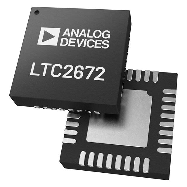


 工商网监
湘ICP备2023018690号
工商网监
湘ICP备2023018690号
