LTC7150S/LTC7150S-4
20V, 20A Synchronous
Step-Down Regulator
FEATURES
DESCRIPTION
AEC-Q100 Qualified for Automotive Applications
nn Silent Switcher ® 2 Architecture for Low EMI
nn V Range: 3.1V to 20V
IN
nn V
OUT Range: 0.6V to 5.5V
nn Differential V
OUT Remote Sense
nn Adjustable Frequency: 400kHz to 3MHz
nn PolyPhase® Operation: Up to 12 Phases
nn Output Tracking and Soft-Start
nn Reference Accuracy: 0.6V ±1% Over Temperature
nn Current Mode Operation for Excellent Line and Load
Transient Response
nn Accurate 1.2V Run Pin Threshold
nn Supports Forced Continuous/Discontinuous Modes
nn 42-Lead 6mm × 5mm × 1.3mm BGA Package
The LTC®7150S is a high efficiency monolithic synchronous
buck regulator capable of delivering 20A to the load. It uses
a phase lockable controlled on-time constant frequency, current mode architecture. PolyPhase operation allows multiple
LTC7150S regulators to run out-of-phase, which reduces
the amount of input and output capacitors required. The
operating supply voltage range is from 3.1V to 20V.
nn
The operating frequency is programmable from 400kHz to
3MHz with an external resistor. The high frequency capability
allows the use of physically smaller inductor and capacitor sizes. For switching noise sensitive applications, the
LTC7150S can be externally synchronized from 400kHz
to 3MHz. The PHMODE pin allows the user control of the
phase of the outgoing clock signal. The unique constant
frequency/controlled on-time architecture is ideal for high
step-down ratio applications that operate at high frequencies
while demanding fast transient response. The LTC7150S
uses second generation Silent Switcher technology including integrated bypass capacitors to deliver a highly efficient
solution at high frequencies with excellent EMI performance.
APPLICATIONS
Server Power Applications
Distributed Power Systems
nn Point of Load Supply for ASIC, FPGA, DSP, µP, etc.
nn
nn
All registered trademarks and trademarks are the property of their respective owners.
PART NUMBER
TJMAX
LTC7150S
125°C
LTC7150S-4
150°C
TYPICAL APPLICATION
12VIN to 1.2VOUT Application
Efficiency and Power Loss
4.7µF
RT
162k
10k
100µF
×2
+
330µF
VOUT–
PGOOD
MODE/SYNC
SGND
ITH
95
10
90
8
85
6
80
4
75
2
70
10k
1nF
EFFICIENCY (%)
PHMODE
TRACK/SS
CLKOUT
INTVCC
10k
FB
LTC7150S
SVIN = 5V
VOUT
1.2V/20A
SW
22pF
0
4
8
12
IOUT (A)
16
20
POWER LOSS (W)
22µF
×2
RUN
PVIN
SVIN
12
100
0.25µH
VIN
3.1V TO 20V
0
7150S TA01b
7150S TA01a
Rev. B
Document Feedback
For more information www.analog.com
1
�LTC7150S/LTC7150S-4
ABSOLUTE MAXIMUM RATINGS
PIN CONFIGURATION
(Note 1)
PVIN, SVIN.................................................. –0.3V to 22V
RUN Voltage............................................. –0.3V to SVIN
MODE/SYNC, TRACK/SS Voltage.......... –0.3V to INTVCC
ITH, RT, PGOOD Voltage............................ –0.3V to 3.6V
PHMODE, CLK Voltage............................... –0.3V to 3.6V
VOUT– Voltage............................................ –0.3V to 0.3V
FB Voltage.................................................. –0.3V to 3.6V
Operating Junction Temperature Range
LTC7150SE......................................... –40°C to 125°C
LTC7150SI.......................................... –40°C to 125°C
LTC7150S-4J...................................... –40°C to 150°C
Storage Temperature Range................... –65°C to 150°C
Maximum Internal Temperature............................. 125°C
Peak Reflow Solder Body Temperature.................. 260°C
TOP VIEW
1
2
3
4
5
6
PGOOD
RT
ITH
FB
VOUT–
A
PHMODE
CLKOUT RUN M/S TRACK/SS SGND INTVCC
B
SVIN
PVIN
SW
SW
PVIN
PVIN
PVIN
PVIN
SW
SW
PVIN
PVIN
PGND PGND
SW
SW
PGND PGND
PGND PGND
SW
SW
PGND PGND
PGND PGND
SW
SW
PGND PGND
C
D
E
F
G
BGA PACKAGE
42-LEAD (6mm × 5mm × 1.30mm)
θJA = 21°C/W
ORDER INFORMATION
PART MARKING*
PART NUMBER
PAD OR BALL FINISH
LTC7150SEY#PBF
LTC7150SIY#PBF
SAC305 (RoHS)
LTC7150SJY-4#PBF
DEVICE
FINISH CODE
PACKAGE
TYPE
MSL
RATING
e1
BGA
3
7150S
7150S4
TEMPERATURE RANGE
(SEE NOTE 2)
–40°C to 125°C
–40°C to 150°C
AUTOMOTIVE PRODUCTS**
LTC7150SJY-4#WPBF
SAC305 (RoHS)
7150S4
e1
BGA
3
–40°C to 150°C
• Contact the factory for parts specified with wider operating temperature
ranges. *Pad or ball finish code is per IPC/JEDEC J-STD-609.
• Recommended LGA and BGA PCB Assembly and Manufacturing
Procedures
• This product is not recommended for second side reflow. see BGA
Assembly and Manufacturing Procedures)
• LGA and BGA Package and Tray Drawings
• This product is moisture sensitive (see BGA Assembly and Manufacturing
Procedures).
**Versions of this part are available with controlled manufacturing to support the quality and reliability requirements of automotive applications. These
models are designated with a #W suffix. Only the automotive grade products shown are available for use in automotive applications. Contact your
local Analog Devices account representative for specific product ordering information and to obtain the specific Automotive Reliability reports for
these models.
2
Rev. B
For more information www.analog.com
�LTC7150S/LTC7150S-4
ELECTRICAL CHARACTERISTICS
The l denotes the specifications which apply over the specified operating
junction temperature range, otherwise specifications are at TA = 25°C (Note 2). VIN = 12V, unless otherwise noted.
SYMBOL
PARAMETER
CONDITIONS
SVIN
SVIN Operating Voltage
PVIN
PVIN Operating Voltage
VOUT
VOUT Operating Voltage
IQ
Input Quiescent Current (Note 3)
Active Mode
Shutdown Mode; VRUN = 0V
VFB
Feedback Reference Voltage (Note 4)
ITH = 1.0V
ITH = 1.0V, –40°C to 150°C
MIN
l
TYP
3.1
0.598
0.594
UNITS
20
V
20
V
5.5
V
2
20
4
40
mA
µA
0.600
0.600
0.602
0.606
V
V
0.6
l
MAX
∆VLINE_REG
Feedback Voltage Line Regulation
VIN = 3.1V to 20V
–40°C to 150°C
l
0.04
%/V
∆VLOAD_REG
Feedback Voltage Load Regulation
ITH = 0.5V to 1.5V
–40°C to 150°C
l
0.2
%
IFB
Feedback Pin Input Current
gm(EA)
Error Amplifier Transconductance
tON(MIN)
Minimum On-Time
tOFF(MIN)
Minimum Off-Time
ILIM
Positive Inductor Valley Current Limit
FB = 0.58V
l
21
24
27
A
ILIM-ITH
Current Limit at Different ITH Voltage
ITH = 1.4V
ITH = 1V
ITH = 0.6V
ITH = 0.2V
l
l
l
l
9.5
–2.5
–14.5
–27
12
0
–12
–24
14.5
2.5
–9.5
–21
A
A
A
A
RTOP
Top Power NMOS On-Resistance
INTVCC = 3.3V
6
mΩ
RBOT
Bottom Power NMOS On-Resistance
INTVCC = 3.3V
2.5
mΩ
ISW
(Note 5)
Top Switch Leakage
Bottom Switch Leakage
VIN = 20V, VSW = 0V
VIN = 20V, VSW = 20V
0.1
1
1
50
µA
µA
VUVLO
INTVCC Undervoltage Lockout Threshold
INTVCC Falling
INTVCC Hysteresis (Rising)
2.45
2.6
250
2.75
V
mV
VRUN
RUN Rising
RUN Falling Hysteresis
1.15
1.20
100
1.25
V
mV
IRUN
Run Leakage Current
100
nA
VINTVCC
Internal VCC Voltage
OV
Output Overvoltage
PGOOD Upper Threshold
UV
–50
ITH = 1.0V
1.0
l
50
nA
1.3
1.6
mS
20
25
nS
50
nS
3.2
3.3
3.4
V
VFB Rising
VFB Falling Hysteresis
6
8
10
10
%
mV
Output Undervoltage
PGOOD Lower Threshold
VFB Falling
VFB Rising Hysteresis
–10
–8
10
–6
%
mV
RPGOOD
PGOOD Pull-Down Resistance
VPGOOD = 100mV
8
15
Ω
IPGOOD
PGOOD Leakage
VFB = 0.6V
2
µA
tPGOOD
PGOOD Delay
PGOOD Low to High
PGOOD High to Low
6
25
ITRACK/SS
Track Pull-Up Current
VTRACK/SS = 0V
6
10
fOSC
Oscillator Frequency
RT = 162kΩ
1
1.15
MHz
fSYNC
SYNC Capture Range
% of Programmed Frequency
130
%
l
0.9
70
cycles
cycles
µA
Rev. B
For more information www.analog.com
3
�LTC7150S/LTC7150S-4
ELECTRICAL CHARACTERISTICS
The l denotes the specifications which apply over the specified operating
junction temperature range, otherwise specifications are at TA = 25°C (Note 2). VIN = 12V, unless otherwise noted.
SYMBOL
PARAMETER
CONDITIONS
MODE/SYNC
MODE/SYNC Threshold Input High
MODE/SYNC Threshold Input Low
IMODE/SYNC
MODE/SYNC Current
VCLKOUT
Clock Output High Voltage
Clock Output Low Voltage
PHMODE
PHMODE Threshold
180° (2-Phase)
90° (4-Phase)
120° (3-Phase)
VINOV
VIN Overvoltage Threshold
VIN Rising
VIN Falling
TYP
MODE/SYNC = 0V
VINTVCC – 0.2
UNITS
V
V
6
14
µA
VINTVCC
0
0.2
V
V
VINTVCC – 1
0.1
V
V
V
26.5
23
V
V
VINTVCC – 0.1
1.0
22.5
20
MAX
1
0.3
Note 1: Stresses beyond those listed under Absolute Maximum Ratings
may cause permanent damage to the device. Exposure to any Absolute
Maximum Rating condition for extended periods may affect device
reliability and lifetime.
Note 2: The LTC7150S is tested under pulsed load conditions such
that TJ ≈ TA. The LTC7150SE is guaranteed to meet specifications from
0°C to 125°C junction temperature. Specifications over the –40°C to
125°C operating junction temperature range are assured by design,
characterization and correlation with statistical process controls. The
LTC7150SI is guaranteed over the –40°C to 125°C operating junction
temperature range. The LTC7150SJ-4 is guaranteed over the –40°C to
150°C operating junction temperature range. Note that the maximum
ambient temperature consistent with these specifications is determined by
4
MIN
24.5
21.5
specific operating conditions in conjunction with board layout, the rated
package thermal impedance and other environmental factors. The junction
temperature
(TJ, in °C) is calculated from the ambient temperature (TA, in °C) and
power dissipation (PD, in Watts) according to the formula:
TJ = TA + (PD • θJA),
where θJA (in °C/W) is the package thermal impedance.
Note 3: The quiescent current in forced continuous mode does not include
switching loss of the power FETs.
Note 4: The LTC7150S is tested in a feedback loop that servos VITH to a
specified voltage and measures the resultant VFB.
Note 5: There is additional switch current due to internal resistor to ground.
Rev. B
For more information www.analog.com
�LTC7150S/LTC7150S-4
T
TYPICAL
PERFORMANCE CHARACTERISTICS A = 25°C, VIN = 12V, VOUT = 1.2V, unless
otherwise noted.
Efficiency vs Load Current 500kHz
Efficiency vs Load Current 1MHz
100
95
95
90
90
85
80
VOUT = 1.0V
VOUT = 1.2V
VOUT = 1.5V
75
70
0
4
8
12
IOUT (A)
16
PVIN = 12V, SVIN = 5V
L = 0.25µH (DCR = 0.37mΩ)
80
70
7150S G01
Transient Response, DCM
90
85
80
VOUT = 1.0V
VOUT = 1.2V
VOUT = 1.5V
0
4
8
PVIN = 12V, SVIN = 5V
L = 0.15µH (DCR = 0.37mΩ)
95
85
75
20
Efficiency vs Load Current 2MHz
100
EFFICIENCY (%)
PVIN = 12V, SVIN = 5V
L = 0.33µH (DCR = 0.37mΩ)
EFFICIENCY (%)
EFFICIENCY (%)
100
12
IOUT (A)
16
VOUT = 1.0V
VOUT = 1.2V
VOUT = 1.5V
75
70
20
0
4
8
7150S G02
Transient Response, CCM
12
IOUT (A)
7150S G03
VOUT = 1.2V
0.75
VOUT
AC–COUPLED
50mV/DIV
0.50
NORMALIZED (%)
IL
10A/DIV
20
Load Regulation vs Load Current
1.00
VOUT
AC–COUPLED
50mV/DIV
16
IL
10A/DIV
0.25
0
–0.25
–0.50
7150S G04
VIN = 12V, VOUT = 1.2V
IOUT = 1.5A TO 15A, L = 0.15µH, fSW = 1MHz
RITH = 20kΩ, CITH = 220pF, CITHP = 22pF
RFB1 = 10kΩ, RFB2 = 10kΩ
COUT = 2 × 100µF + 2 × 330µF
RDS(ON)
vsTemperature
Temperature
RDS
ON vs
Output Tracking
20µs/DIV
–0.75
–1.00
40
10
VTRACK/SS
500mV/DIV
8
VOUT
1V/DIV
6
IL
10A/DIV
4
0
4
8
12
IOUT (A)
16
20
7150S G06
Shutdown Current vs VIN
30
IQ (uA)
RDS(ON) (mΩ)
12
7150S G05
20µs/DIV
VIN = 12V, VOUT = 1.2V
IOUT = 1.5A to 15A, L = 0.15µH, fSW = 1MHz
RITH = 10kΩ, CITH = 1.0nF, CITHP = 100pF
RFB1 = 10kΩ, RFB2 = 10kΩ
COUT = 2 × 100uF + 2 × 330µF
20
10
2
0
–50 –25
BOT FET
TOP FET
0
25 50 75 100 125 150
TEMPERATURE (°C)
200µs/DIV
7150S G08
VIN = 12V, ROUT = 0.1Ω
RFB1 = 10kΩ, RFB2 = 10kΩ
VTRACK = 0V to 1V
7150S G07
0
0
5
10
VIN (V)
15
20
7150S G09
Rev. B
For more information www.analog.com
5
�LTC7150S/LTC7150S-4
T
TYPICAL
PERFORMANCE CHARACTERISTICS A = 25°C, VIN = 12V, VOUT = 1.2V, unless
otherwise noted.
3.5
100
ISVIN (mA)
75
50
25
0
0.4
SVIN = 5V
FC MODE
0.9
1.5
2.0
FREQUENCY (MHz)
2.0
1.5
75
0.5
0
50
80
12
PVIN (V)
16
0.9
1.4
2.0
FREQUENCY (MHz)
RT = 162kΩ
1.3
55
1.2
1.1
1.0
DEMOBOARD ON
STILL AIR, TA = 25°C
0
2
4
6
8
0.9
10 12 14 16 18 20
IOUT (A)
0
2
4
6
VOUT (V)
7150S G14
7150S G13
Regulated FB Voltage
vs Temperature
RUN Rising Threshold
vs Temperature
8
10
7150S G15
Frequency vs Temperature
1.220
605
3
Switching Frequency vs VOUT
70
25
20
2.5
1.4
40
IOUT = 10A
IOUT = 20A
8
0.4
7150S G12
FREQUENCY (MHz)
DIE TEMPERATURE (°C)
EFFICIENCY (%)
70
100 150 200 250 300 350 400
RT (kΩ)
PVIN = 12V
SVIN = 5V
VOUT = 1.2V
fSW = 1MHz
85
85
4
80
Die Temperature vs Load
90
70
IOUT = 20A
85
1.0
100
SVIN = 5V
fSW = 1MHz
L = 0.25µH
75
IOUT = 10A
90
7150S G11
Efficiency vs PVIN
95
L = 0.25µH
95
2.5
7150S G10
100
Efficiency vs Frequency
100
3.0
0
2.5
Switching Frequency vs RT
EFFICIENCY (%)
SVIN Current vs Frequency, CCM
SWITCHING FREQUENCY (MHz)
125
1.100
601
599
597
595
–50 –25
0
25 50 75 100 125 150
TEMPERATURE (°C)
7150S G16
6
1.050
FREQUENCY (MHz)
603
RUN RISING THRESHOLD (V)
REGULATED FB VOLTAGE (mV)
RT = 162kΩ
1.215
1.210
1.205
1.200
1.000
0.950
1.195
1.190
–50 –25
0
25 50 75 100 125 150
TEMPERATURE (°C)
7150S G17
0.900
–50 –25
0
25 50 75 100 125 150
TEMPERATURE (°C)
7150S G18
Rev. B
For more information www.analog.com
�LTC7150S/LTC7150S-4
TYPICAL PERFORMANCE CHARACTERISTICS
TA = 25°C, VIN = 12V, VOUT = 1.2V, unless
otherwise noted.
Discontinuous Conduction Mode
Operation
Continuous Conduction Mode
Operation
5.00
CLKOUT
5V/DIV
SW
10V/DIV
IL
5A/DIV
IL
10A/DIV
7150S G19
1µs/DIV
6
VIN = 12V, VOUT = 1.2V
IOUT = 0A, L = 0.15µH, fSW = 1MHz
4.20
3.80
3.40
3.00
Active Current vs SVIN,
DCM No Load
Period Jitter vs IP-P
VRUN
2V/DIV
2.0
VPGOOD
5V/DIV
1.5
VOUT
1V/DIV
2
1.0
IL
10A/DIV
1
0.5
IQ (mA)
4
3
4
6
8
IPK–PK (A)
10
0
12
VRUN
2V/DIV
VPGOOD
5V/DIV
VOUT
1V/DIV
IL
10A/DIV
7150S G25
VALLEY CURRENT LIMIT (A)
24
VIN = 12V, CTRACK/SS = 0.1µF
ROUT = 0.1Ω, L = 0.15µH, fSW = 1MHz
RFB1 = 10kΩ, RFB2 = 10kΩ
COUT = 2 × 100µF + 2 × 330µF
0
5
10
SVIN (V)
7150S G22
Start-Up with Pre-Biased Output
2ms/DIV
400
500
7150S G21
15
7150S G24
VIN = 12V, CTRACK/SS = 0.1µF
ROUT = 0.1Ω, L = 0.15µH, fSW = 1MHz
RFB1 = 10kΩ, RFB2 = 10kΩ
COUT = 2 × 100µF + 2 × 330µF
20
7150S G23
Valley Current Limit
vs Temperature
Valley Current Limit vs VITH
26
16
VALLEY CURRENT LIMIT (A)
2
200
300
t ON (ns)
2ms/DIV
VTRACK = 0V
0
100
Start-Up Waveform
2.5
0
0
3.0
VIN = 12V
VOUT = 1.2V
fSW = 1MHz
5
PERIOD JITTER 1σ (ns)
7150S G20
500ns/DIV
VIN = 12V, VOUT = 1.2V
IOUT = 1.5A, L = 0.15µH, fSW = 1MHz
fSW = 1MHz
IP-P = 6A
4.60
PERIOD JITTER 1σ (ns)
SW
5V/DIV
Period Jitter vs tON
8
0
–8
–16
–24
0.2
0.4
0.6
0.8
1 1.2
VITH (V)
1.4
1.6
1.8
7150S G26
25
24
23
22
–50 –25
0
25 50 75 100 125 150
TEMPERATURE (°C)
7150S G27
Rev. B
For more information www.analog.com
7
�LTC7150S/LTC7150S-4
PIN FUNCTIONS
PHMODE (Pin A1): Control Input to Phase Selector.
Determines the phase relationship between internal
oscillator and CLKOUT. Tie it to INTVCC for 2-phase
operation, tie it to SGND for 3-phase operation, and tie it
to INTVCC/2 (or float the pin) for 4-phase operation.
PGOOD (Pin A2): Output Power Good with Open-Drain
Logic. PGOOD is pulled to ground when the voltage of the
FB pin is not within ±8% of the internal 0.6V reference.
RT (Pin A3): Switching Frequency Programming Pin.
Connect an external resistor (between 405k to 54k) from
this pin to GND to program the frequency from 400kHz
to 3MHz.
ITH (Pin A4): Error Amplifier Output and Switching
Regulator Compensation Point. The current comparator’s
trip threshold is linearly proportional to this voltage,
whose normal range is from 0.3V to 1.8V.
FB (Pin A5): Feedback Input to the Error Amplifier of the
Step-Down Regulator. Connect resistor divider tap to this
pin. The output voltage can be adjusted from 0.6V to VIN
by: VOUT = 0.6V • [1 + (R1/R2)].
VOUT– (Pin A6): Negative Return of Output Rail. Connect
this pin directly to the bottom of the remote output
capacitor near the load in order to minimize error incurred
by voltage drop across the metal trace of the board.
CLKOUT (Pin B1): Output Clock Signal for PolyPhase
Operation. The phase of CLKOUT with respect to CLKIN
is determined by the state of the PHMODE pin. CLKOUT’s
peak-to-peak amplitude is INTVCC to GND.
RUN (Pin B2): Logic Controlled RUN Input. Do not leave this
pin floating. Logic High activates the step-down regulator.
8
MODE/SYNC (Pin B3): Discontinuous Mode Select
and Oscillator Synchronization Pin. Tie MODE/SYNC
to GND for discontinuous mode of operation. Floating
MODE/SYNC or tying it to a voltage above 1V will select
forced continuous mode. Furthermore, connecting MODE/
SYNC to an external clock will synchronize the system
clock to the external clock and puts the part in forced
continuous mode.
TRACK/SS (Pin B4): Output Tracking and Soft-Start Pin.
Allows the user to control the rise time of the output
voltage. Putting a voltage between 0.6V on this pin relative
to VOUT– bypasses the internal reference input to the error
amplifier, instead it servos the FB pin relative to VOUT– to
that voltage. There’s an internal 5µA pull-up current from
INTVCC to this pin, so putting a capacitor from this pin to
VOUT– provides a soft-start function.
SGND (Pin B5): Signal GND.
INTVCC (Pin B6): Internal 3.3V Regulator Output. The
internal power drivers and control circuits are powered
from this voltage. Decouple this pin to power ground with
a minimum of 4.7µF low ESR ceramic capacitor.
SVIN (Pin C1): Signal VIN. Filtered input voltage to the
on-chip 3.3V regulator. Bypass signal into the SVIN pin
with a 0.1µF ceramic capacitor.
PVIN (Pins C2, C5, C6, D1, D2, D5, D6): Power VIN. Input
voltage to the on chip power MOSFETs.
SW (Pins C3, C4, D3, D4, E3, E4, F3, F4, G3, G4):
Switch Node Connection of External Inductor. Voltage
swing of SW is from a diode voltage drop below ground
to a diode voltage above PVIN.
PGND (Pins E1, E2, E5, E6, F1, F2, F5, F6, G1, G2, G5,
G6): Ground for Power and Signal Ground.
Rev. B
For more information www.analog.com
�LTC7150S/LTC7150S-4
BLOCK DIAGRAM
SW
LTC7150S
MTOP
PVIN
0.2µF
(0.02µF FOR LTC7150S-4) PGND
BOOST
SVIN
0.22µF
(0.047µF FOR
LTC7150S-4)
INTVCC
MBOT
RUN
LDO
INTVCC
GATEDRIVE
+
REVERSE CURRENT
COMPARATOR
–
+
–
+
LOGIC
CURRENT
COMPARATOR
VOUT–
TRACK/SS
0.6V
+
+
–
TRACK
AMPLIFIER
–
+
–
MODE/SYNC
PHMODE
CLK_INT
OSCILLATOR
INTVCC
ERROR
AMPLIFIER
FB
ITH
CLKOUT
PVIN
FB
PGOOD
POWER
GOOD
STATUS
SGND
SW
ON TIME
CALCULATOR
RT
7150S BD
Rev. B
For more information www.analog.com
9
�LTC7150S/LTC7150S-4
OPERATION
Main Control Loop
The LTC7150S is a current mode monolithic 20A stepdown regulator. In normal operation, the internal top power
MOSFET is turned on for a fixed interval determined by a
one-shot timer, OST. When the top power MOSFET turns
off, the bottom power MOSFET turns on until the current
comparator, ICMP, trips, restarting the one-shot timer and
initiating the next cycle. Inductor current is determined
by sensing the voltage drop across the bottom power
MOSFET when it is on. The voltage on the ITH pin sets
the comparator threshold corresponding to the inductor
valley current. The error amplifier, EA, adjusts this ITH
voltage by comparing the feedback signal, VFB, with an
internal 0.6V reference. If the load current increases, it
causes a drop in the feedback voltage relative to the internal reference, the ITH voltage then rises until the average
inductor current matches that of the load current.
At low load currents, the inductor current can drop to zero
and become negative. In discontinuous mode (DCM), this
is detected by the current reversal comparator, IREV, which
then shuts off the bottom power MOSFET. Both power
MOSFETs will remain off with the output capacitor supplying the load current until the ITH voltage rises above zero
current level to initiate the next cycle. If continuous mode
of operation is desired, simply float the MODE/SYNC pin
or tie it to INTVCC.
The operating frequency is determined by the value of the
RT resistor, which programs the current for the internal
oscillator. An internal phase-lock loop servos the oscillator frequency to an external clock signal if one is present on the MODE/SYNC pin. Another internal phase-lock
loop servos the switching regulator on-time to track the
internal oscillator to force a constant switching frequency.
Overvoltage and undervoltage comparators OV and UV
pull the PGOOD output low if the output feedback voltage, VFB, exits a ±8% window around the regulation point.
Continuous operation is forced during OV and UV conditions except during start-up when the TRACK pin is ramping up to 0.6V.
10
The “S” in LTC7150S refers to the second generation
Silent Switcher technology. The IC has integrated ceramic
capacitors for VIN and BOOST to keep all the fast AC current loops small, thus improving the EMI performance.
Furthermore, it allows for faster switching edges which
greatly improves efficiency at high switching frequencies.
RUN Threshold
Pulling the RUN pin to ground forces the LTC7150S into
its shutdown state. Bringing the RUN pin to above 0.6V
will turn on the internal reference only, while keeping the
power MOSFETs off. Further increasing the RUN voltage
above the RUN rising threshold (nominally 1.2V) turns on
the entire chip. The accurate 1.2V RUN threshold allows
the user to program the SVIN under voltage lockout
threshold by placing a resistor divider from SVIN.
INTVCC Regulator
An internal low dropout (LDO) regulator produces the 3.3V
supply that powers the drivers and internal bias circuitry.
The INTVCC must be bypassed to ground with a minimum
of a 4.7µF ceramic capacitor. Good bypassing is necessary to supply the high transient currents required by the
power MOSFET gate drivers. Applications with high input
voltage and high switching frequency will experience an
increase in die temperature due to the higher power dissipation across the LDO. In such cases, if there’s another
5V or 3.3V supply rail available, consider using that to
drive the SVIN pin to lower the power dissipation across
the internal LDO.
VIN Overvoltage Protection
In order to protect the internal power MOSFET devices
against transient voltage spikes, the LTC7150S constantly
monitors the PVIN pin for an overvoltage condition. When
the PVIN rises above 24.5V, the regulator suspends operation by shutting off both power MOSFETs. Once PVIN drops
below 21.5V, the regulator immediately resumes normal
operation. During an overvoltage event, the internal softstart voltage is clamped to a voltage slightly higher than
the feedback voltage, thus the soft-start feature will be
present upon exiting an overvoltage condition.
Rev. B
For more information www.analog.com
�LTC7150S/LTC7150S-4
OPERATION
Output Voltage Programming
The output voltage is set by an external resistive divider
according to the following equation:
⎛ R1⎞
VOUT = 0.6V • ⎜ 1+ ⎟
⎝ R2 ⎠
The resistive divider allows the VFB pin to sense a fraction of the output voltage as shown in Figure 1. Since the
LTC7150S will often be used in high power applications,
there can be significant voltage drop due to board layout
between the part and the point of load (POL). Thus, it is
imperative to have R2 and R1 Kelvin directly to the positive
and negative terminals of the point of load. The negative
terminal should then be connected directly to the VOUT–
pin of the LTC7150S for differential VOUT sensing. A feed
forward compensation capacitor, CFF, can also be placed
between VOUT and FB to improve transient performance.
In applications where the POL is far from the IC, it is a
good idea to place a 0.1µF capacitor from VOUT– to GND
close to the IC to filter any noise that might be injected
onto the VOUT– trace.
VOUT
R1
CFF
FB
LTC7150S
VOUT
R2
–
KELVIN TO POINT
OF LOAD GND
7150S F01
Figure 1. Setting the Output Voltage Differentially
Programming Switching Frequency
Connecting a resistor from the RT pin to SGND programs
the switching frequency from 400kHz to 3MHz according
to the following formula:
Frequency =
1.67 • 1011
RT (Ω)
The internal PLL has a synchronization range of ±30%
around its programmed frequency. Therefore, during external clock synchronization be sure that the
external clock frequency is within this ±30% range
of the RT programmed frequency. See plot of switching frequency vs RT value in the Typical Performance
Characteristics section.
Output Voltage Tracking and Soft-Start
The LTC7150S allows the user to program its output voltage ramp rate by means of the TRACK/SS pin. An internal
6µA current pulls up the TRACK/SS pin to INTVCC. Putting
an external capacitor on TRACK/SS enables soft starting
the output to prevent current surge on the input supply. For output tracking applications, TRACK/SS can be
externally driven by another voltage source. From 0V to
0.6V, the TRACK/SS voltage will override the internal 0.6V
reference input to the error amplifier, thus regulating the
feedback voltage to that of the TRACK/SS pin. During this
start-up time, the LTC7150S will operate in discontinuous
mode. When TRACK/SS is above 0.6V, tracking is disabled and the feedback voltage will regulate to the internal
reference voltage. The relationship between output rise
time and TRACK/SS capacitance is given by:
TSS = 120000 • CTRACK/SS
A default internal soft-start ramp forces a minimum softstart time of 100µs by overriding the TRACK/SS pin input
during this time period. Hence, capacitance values less
than approximately 820pF will not significantly affect softstart behavior.
Multiphase Operation
For output loads that demand more than 20A of current,
multiple LTC7150Ss can be paralleled to run out-of-phase
to provide more output current. The MODE/SYNC pin allows
the LTC7150S to synchronize to an external clock and the
internal phase-locked-loop allows the LTC7150S to lock
onto MODE/SYNC’s phase as well. The CLKOUT signal
can be connected to the MODE/SYNC pin of the following
LTC7150S to line up both the frequency and the phase of
the entire system. Tying the PHMODE pin to INTVCC, SGND
or floating the pin generates a phase difference between the
clock applied on the MODE/SYNC pin and CLKOUT of 180°
degrees, 120° degrees, or 90° degrees respectively, which
corresponds to 2-phase, 3-phase, or 4-phase operation. A
total of 12 phases can be paralleled to run simultaneously
out-of-phase with respect to each other by programming the
PHMODE pin of each LTC7150S to different voltage levels.
For more information www.analog.com
Rev. B
11
�LTC7150S/LTC7150S-4
OPERATION
External ITH Compensation
External compensation is mandatory for proper operation of the LTC7150S. Proper ITH components should be
selected for OPTI-LOOP® optimization. The compensation
network is shown in Figure 2.
ITH
CITH
CITHP
7150S F02
Figure 2. External Compensation Network
Table 1 provides a basic guideline for the compensation values that should be used given the frequency of
the part. Slight tweaks to those values may be required
depending on the amount of output capacitance used in
the application.
Table 1. Compensation Values
Frequency
RITH
CITH
CITHP
500kHz
4.99k
1.5nF
47pF
1MHz
10k
1nF
22pF
2MHz
15k
0.68nF
15pF
3MHz
20k
0.47nF
10pF
Minimum Off-Time and Minimum On-Time
Considerations
The minimum off-time, tOFF(MIN), is the smallest amount
of time that the LTC7150S is capable of turning on the bottom power MOSFET, tripping the current comparator and
turning the power MOSFET back off. This time is generally
about 50ns. The minimum off-time limit imposes a maximum duty cycle of tON /(tON + tOFF(MIN)). If the maximum
duty cycle is reached, due to a dropping input voltage for
example, then the output will drop out of regulation. The
minimum input voltage to avoid dropout is:
12
DCMIN = f • tON(MIN)
Where tON(MIN) is the minimum on-time. Reducing the
operating frequency will alleviate the minimum duty cycle
constraint.
RITH
VIN(MIN) = VOUT •
Conversely, the minimum on-time is the smallest duration of time in which the top power MOSFET can be in
its “on” state. This time is typically 20ns. In continuous
mode operation, the minimum on-time limit imposes a
minimum duty cycle of
tON + tOFF(MIN)
tON
In the rare cases where the minimum duty cycle is surpassed, the output voltage will still remain in regulation,
and the switching frequency will decrease from its programmed value. This is an acceptable result in many
applications, so this constraint may not be of critical
importance in most cases. High switching frequencies
may be used in the design without any fear of output
overvoltage. As the sections on inductors and capacitor
selection show, high switching frequencies allow the use
of smaller board components, thus reducing the size of
the application circuit.
Input Capacitor (CIN) Selection
The input capacitance, CIN, is needed to filter the square
wave current at the drain of the top power MOSFET. To
prevent large voltage transients from occurring, a low
ESR input capacitor sized for the maximum RMS current
should be used. The maximum RMS current is given by:
V
IRMS ≅ IOUT(MAX) OUT
VIN
VIN
VOUT
−1
This formula has a maximum at VIN = 2VOUT, where
IRMS ≅
IOUT
2
This simple worst-case condition is commonly used for
design because even significant deviations do not offer
much relief. Note that ripple current ratings from capacitor manufacturers are often based on only 2000 hours of
life which makes it advisable to further derate the capacitor, or choose a capacitor rated at a higher temperature
than required. Several capacitors may also be paralleled
to meet size or height requirements in the design. For low
Rev. B
For more information www.analog.com
�LTC7150S/LTC7150S-4
OPERATION
input voltage applications, sufficient bulk input capacitance is needed to minimize transient effects during output load changes.
Output Capacitor (COUT) Selection
The selection of COUT is determined by the effective series
resistance (ESR) that is required to minimize voltage ripple and load step transients as well as the amount of bulk
capacitance that is necessary to ensure that the control
loop is stable. Loop stability can be checked by viewing
the load transient response. The output ripple, ΔVOUT, is
determined by:
⎛
⎞
1
ΔVOUT < ΔIL ⎜
+ ESR⎟
⎝ 8 • f • COUT
⎠
The output ripple is highest at maximum input volt-age
since ΔIL increases with input voltage. Multiple capacitors
placed in parallel may be needed to meet the ESR and
RMS current handling requirements. Dry tantalum, special polymer, aluminum electrolytic, and ceramic capacitors are all available in surface mount packages. Special
polymer capacitors are very low ESR but have lower
capacitance density than other types. Tantalum capacitors
have the highest capacitance density but it is important
to only use types that have been surge tested for use in
switching power supplies. Aluminum electrolytic capacitors have significantly higher ESR, but can be used in
cost-sensitive applications provided that consideration
is given to ripple current ratings and long-term reliability.
Ceramic capacitors have excellent low ESR characteristics
and small footprints.
VIN input. At best, this ringing can couple to the output
and be mistaken as loop instability. At worst, a sudden
in-rush of current through the long wires can potentially
cause a voltage spike at VIN large enough to damage the
part.
When choosing the input and output ceramic capacitors,
choose the X5R and X7R dielectric formulations. These
dielectrics have the best temperature and voltage characteristics of all the ceramics for a given value and size.
Since the ESR of a ceramic capacitor is so low, the input
and output capacitor must instead fulfill a charge storage requirement. During a load step, the output capacitor must instantaneously supply the current to support
the load until the feedback loop raises the switch current enough to support the load. Typically, 5 cycles are
required to respond to a load step, but only in the first
cycle does the output voltage drop linearly. The output
droop, VDROOP, is usually about 3 times the linear drop of
the first cycle. Thus, a good place to start with the output
capacitor value is approximately:
COUT = 3
ΔIOUT
fO • VDROOP
More capacitance may be required depending on the duty
cycle and load step requirements. In most applications,
the input capacitor is merely required to supply high frequency bypassing, since the impedance to the supply is
very low. A 47μF ceramic capacitor is usually enough for
these conditions. Place this input capacitor as close to the
PVIN pin as possible.
Inductor Selection
Using Ceramic Input and Output Capacitors
Higher values, lower cost ceramic capacitors are now
becoming available in smaller case sizes. Their high ripple
current, high voltage rating and low ESR make them ideal
for switching regulator applications. However, care must
be taken when these capacitors are used at the input and
output. When a ceramic capacitor is used at the input
and the power is supplied by a wall adapter through long
wires, a load step at the output can induce ringing at the
Given the desired input and output voltages, the inductor value and operating frequency determine the ripple
current:
IL =
VOUT
V
1 OUT
f •L
VIN
Lower ripple current reduces core losses in the inductor,
ESR losses in the output capacitors and output voltage
Rev. B
For more information www.analog.com
13
�LTC7150S/LTC7150S-4
OPERATION
ripple. Highest efficiency operation is obtained at low frequency with small ripple current. However, achieving this
requires a large inductor. There is a trade-off between
component size, efficiency and operating frequency.
A reasonable starting point is to choose a ripple current
that is about 50% of IOUT(MAX). To guarantee that ripple
current does not exceed a specified maximum, the inductance should be chosen according to:
VOUT
VOUT
L=
1
f • IL(MAX)
VIN(MAX)
Once the value for L is known, the type of inductor must
be selected. Actual core loss is independent of core size
for a fixed inductor value, but is very dependent on the
inductance selected. As the inductance or frequency
increases, core losses decrease. Unfortunately, increased
inductance requires more turns of wire and therefore copper losses will increase.
Ferrite designs have very low core losses and are preferred at high switching frequencies, so design goals can
concentrate on copper loss and preventing saturation.
Ferrite core material saturates “hard," which means that
inductance collapses abruptly when the peak design current is exceeded. This results in an abrupt increase in
inductor ripple current and consequent output voltage
ripple. Do not allow the core to saturate!
Different core materials and shapes will change the size/
current and price/current relationship of an inductor.
Toroid or shielded pot cores in ferrite or permalloy materials are small and don’t radiate much energy, but generally
cost more than powdered iron core inductors with similar
characteristics. The choice of which style inductor to use
mainly depends on the price versus size requirements
and any radiated field/EMI requirements. New designs for
surface mount inductors are available from Toko, Vishay,
NEC/Tokin, Cooper, TDK and Wurth Elektronik. Refer to
Table 2 for more details.
Checking Transient Response
The OPTI-LOOP compensation allows the transient
response to be optimized for a wide range of loads and
output capacitors. The availability of the ITH pin not only
allows for optimization of the control loop behavior but
also provides a DC coupled and AC filtered closed loop
response test point. The DC step, rise time and settling
at this test point truly reflects these close loop response.
Assuming a predominantly second order system, phase
margin and/or damping factor can be estimated using the
percentage of overshoot seen at this pin.
The ITH external component shown in the table 1 circuit
will provide an adequate starting point for most applications. The RC filter sets the dominant pole-zero loop
compensation. The values can be modified slightly (from
0.5 to 2 times their suggested value) to optimize transient
response once the final PC layout is done and the particular output capacitor type and value have been determined.
The output capacitors need to be selected because their
various types and values determine the loop feedback
factor gain and phase. An output current pulse of 20%
to 100% of full load current having a rise time of 1µs to
10µs will produce output voltage and ITH pin waveforms
that will give a sense of the overall loop stability without
breaking the feedback loop.
Switching regulators take several cycles to respond to
a step in load current. When a load step occurs, VOUT
Table 2. Inductor Selection Table (Examples)
VENDOR
Part Number
INDUCTANCE (nH)
MAX CURRENT (A)
DC RESISTANCE (mΩ)
DIMENSIONS (mm)
HEIGHT (mm)
Wurth
744308015
150
25
0.37
10 × 7
6.8
744308033
330
25
0.37
10 × 7
6.8
XAL7030-161ME
160
32.5
1.15
7.5 × 7.5
3.1
XAL7070-301ME
300
33.4
1.06
7.5 × 7.2
7.0
PA0511.850NLT
85
31
0.39
10.2 × 7
4.96
PA0512.151NLT
150
24
0.32
7×7
4.96
Coilcraft
Pulse
14
Rev. B
For more information www.analog.com
�LTC7150S/LTC7150S-4
OPERATION
immediately shifts by an amount equal to the ΔILOAD • ESR,
where ESR is the effective series resistance of COUT.
ΔILOAD also begins to charge or discharge COUT generating a feedback error signal used by the regulator to
return VOUT to its steady-state value. During this recovery
time, VOUT can be monitored for overshoot or ringing that
would indicate a stability problem.
The initial output voltage step may not be within the
bandwidth of the feedback loop, so the standard second
order overshoot/DC ratio cannot be used to determine
phase margin. The gain of the loop increases with the RITH
and the bandwidth of the loop increases with decreasing
CITH. If RITH is increased by the same factor that CITH
is decreased, the zero frequency will be kept the same,
thereby keeping the phase the same in most critical frequency ranges of the feedback loop.
The output voltage settling behavior is related to the stability of the closed-loop system and will demonstrate the
actual overall supply performance. For detailed explanation of optimizing the compensation components, including a review of control loop theory, refer to Analog Devices
Application Note 76.
In some applications, a more severe transient can be
caused by switching in loads with large (>47µF) input
capacitors. The discharge input capacitors are effectively
put in parallel with COUT, causing a rapid drop in VOUT. No
regulator can deliver enough current to prevent this problem if the switch connecting the load has low resistance
and is driven quickly. The solution is to limit the turn-on
speed of the load switch driver. A Hot Swap™ controller is designed specifically for this purpose and usually
incorporates current limiting, short-circuit protection, and
soft-starting.
Efficiency Considerations
The percent efficiency of a switching regulator is equal to
the output power divided by the input power times 100%.
It is often useful to analyze individual losses to determine
what is limiting the efficiency and which change would
produce the most improvement. Percent efficiency can
be expressed as:
% Efficiency = 100% – (L1 + L2 + L3 +…)
where L1, L2, etc. are the individual losses as a percentage of input power. Although all dissipative elements in
the circuit produce losses, three main sources usually
account for most of the losses in LTC7150S circuits:
1) I2R losses, 2) switching and biasing losses, 3) other
losses.
1. I2R losses are calculated from the DC resistances of
the internal switches, RSW, and external inductor, RL.
In continuous mode, the average output current flows
through inductor L but is “chopped” between the internal top and bottom power MOSFETs. Thus, the series
resistance looking into the SW pin is a function of both
top and bottom MOSFET RDS(ON) and the duty cycle
(DC) as follows:
RSW = (RDS(ON)TOP)(DC) + (RDS(ON)BOT)(1-DC)
The RDS(ON) for both the top and bottom MOSFETs
can be obtained from the Typical Performance
Characteristics curves. Thus to obtain I2R losses:
I2R losses = IOUT2(RSW + RL)
2. The switching current is the sum of the MOSFET driver
and control currents. The power MOSFET driver current results from switching the gate capacitance of the
power MOSFETs. Each time a power MOSFET gate is
switched from low to high to low again, a packet of
charge dQ moves from IN to ground. The resulting dQ/
dt is a current out of IN that is typically much larger
than the DC control bias current. In continuous mode,
IGATECHG = f(QT + QB), where QT and QB are the gate
charges of the internal top and bottom power MOSFETs
and f is the switching frequency. The power loss is
thus:
Switching Loss = IGATECHG • VIN
The gate charge loss shows up as current through the
INTVCC LDO and becomes larger as frequency increases.
Thus, their effects will be more pronounced in applications with higher input voltage and higher frequency.
3. Other “hidden” losses such as transition loss and copper trace and internal load resistances can account for
additional efficiency degradations in the overall power
system. It is very important to include these “system”
level losses in the design of a system. Transition loss
Rev. B
For more information www.analog.com
15
�LTC7150S/LTC7150S-4
OPERATION
Thermal Considerations
arises from the brief amount of time the top power
MOSFET spends in the saturated region during switch
node transitions. The LTC7150S internal power devices
switch quickly enough that these losses are not significant compared to other sources. Other losses including
diode conduction losses during dead-time and inductor
core losses which generally account for less than 2%
total additional loss.
In some applications where the LTC7150S is operated at a
combination of high ambient temperature, high switching
frequency, high VIN, and high output load, the required
power dissipation might push the part to exceed its maximum junction temperature. If the junction temperature
reaches approximately 175°C, both power switches will
be turned off until the temperature returns to 165°C.
To avoid the LTC7150S from exceeding the maximum
junction temperature, maximum current rating shall
be derated depending on the operating conditions. The
25
15
10
5
0
0LFM
200LFM
400LFM
0
25
50
75
100
AMBIENT TEMPERATURE (°C)
20
15
10
5
0
125
0LFM
200LFM
400LFM
0
25
50
75
100
AMBIENT TEMPERATURE (°C)
7150S F03
MAXIMUM LOAD CURRENT (A)
MAXIMUM LOAD CURRENT (A)
25
15
10
5
0
0LFM
200LFM
400LFM
0
25
50
75
100
AMBIENT TEMPERATURE (°C)
125
7150S F06
Figure 6. Current Derating at
1MHz, 12VSVIN
16
10
5
0LFM
200LFM
400LFM
0
25
50
75
100
AMBIENT TEMPERATURE (°C)
Figure 5. Current Derating at
1MHz, 5VSVIN
25
VSVIN = 5V
VPVIN = 12V
20
15
10
5
0
0LFM
200LFM
400LFM
0
125
7150S F05
Figure 4. Current Derating at
500kHz, 12VSVIN
VSVIN = 12V
VPVIN = 12V
20
15
7150S F04
Figure 3. Current Derating at
500kHz, 5VSVIN
25
VSVIN = 5V
VPVIN = 12V
20
0
125
MAXIMUM LOAD CURRENT (A)
20
25
VSVIN = 12V
VPVIN = 12V
MAXIMUM LOAD CURRENT (A)
VSVIN = 5V
VPVIN = 12V
MAXIMUM LOAD CURRENT (A)
MAXIMUM LOAD CURRENT (A)
25
25
50
75
100
AMBIENT TEMPERATURE (°C)
125
7150S F07
Figure 7. Current Derating at
2MHz, 5VSVIN
VSVIN = 12V
VPVIN = 12V
20
15
10
5
0
0LFM
200LFM
400LFM
0
25
50
75
100
TEMPERATURE (°C)
125
7150S F08
Figure 8. Current Derating at
2MHz, 12VSVIN
Rev. B
For more information www.analog.com
�LTC7150S/LTC7150S-4
OPERATION
temperature rise of the part will vary depending on the
thickness of copper on the PCB board, the number of layers of the board, and the shape of copper trace. In general,
a thick continuous piece of copper on the top layer of the
PCB for SW and GND pins will greatly improve the thermal
performance of the part.
Figure 3 to Figure 8 shows typical derating curves of the
LTC7150S on a standard 6-layer, 2oz copper per layer PCB
board (LTC7150S standard demo board). VOUT is set to
1.2V in all curves.
Silent Switcher Architecture
The LTC7150S has integrated capacitors that allow it
to operate at high switching frequencies efficiently. The
internal VIN bypass capacitors allow the SW edges to
transition extremely fast, effectively reducing transition
CIN
loss. The capacitors also greatly reduces SW overshoot
during top FET turn-on which improves the robustness
of the device over time.
Board Layout Considerations
When laying out the printed circuit board, the following
checklist should be used to ensure proper operation of
the LTC7150S (refer to Figure 9). Check the following in
your layout:
1. Are there pairs of capacitors (CIN) between VIN and
GND as close as possible on both sides of the package?
These capacitors provide the AC current to the internal
power MOSFETs and their drivers as well as minimize
EUI/EMC emissions.
2. Are COUT and L closely connected? The (–) plate of
COUT returns current to GND and the (–) plate of CIN.
CIN
Figure 9. Example of Top Layer PCB Design
Rev. B
For more information www.analog.com
17
�LTC7150S/LTC7150S-4
OPERATION
3. Place the FB dividers close to the part with Kelvin connections to VOUT and VOUT– at the point of load, for
differential VOUT sensing.
For a typical soft start time of 2ms (0% to 100% of final
VOUT value), the CTRACK/SS should be:
4. Keep sensitive components away from the SW pin. The
FB resistors, RT resistor, the compensation component,
and the INTVCC bypass caps should be routed away
from the SW trace and the inductor.
5. A ground plane is preferred.
Because efficiency is important at both high and low load
current, discontinuous mode operation will be utilized.
Select from the characteristic curves the correct RT resistor for the 1MHz switching frequency. Based on that, RT
should be 162kΩ. Then calculate the inductor value to
achieve a current ripple that is about 40% of the maximum
output current (20A) at maximum VIN:
6. Flood all unused areas on all layers with copper, which
reduces the temperature rise of power components.
These copper areas should be connected to GND.
Design Example
As a design example, consider the LTC7150S in an application with the following specifications:
6µA = C TRACK /SS •
0.6V
2ms
CTRACK/SS = 20nF
A typical 22nF capacitor can be used for CTRACK/SS.
⎛ 1.2V ⎞ ⎛ 1.2V ⎞
L=⎜
1−
⎟ = 0.138µH
⎝ 1MHz • 8A ⎟⎠ ⎜⎝
15V ⎠
VIN = 12V to 15V
VOUT = 1.2V
The closest standard value inductor higher would be
0.15µH.
IOUT(MAX) = 20A
IOUT(MIN) = 1A
fSW = 1MHz
First, RFB1 and RFB2 should be the same value in order to
program the output to 1.2V. A typical value that can be
used here for both resistors is 10kΩ. For best accuracy,
a 0.1% resistor should be used.
COUT will be selected based on the ESR that is required to
satisfy the output ripple requirement and the bulk capacitance needed for loop stability. For this design, two 100µF
ceramic capacitors will be used.
CIN should be sized for a maximum current rating of:
⎛ 1.2V ⎞ ⎛ 15V ⎞
IRMS = 20A ⎜
−1
⎝ 15V ⎟⎠ ⎜⎝ 1.2V ⎟⎠
1/2
= 5.4A
Decoupling VIN with two 22µF ceramic capacitors, as
shown in Figure 9, is adequate for most applications.
18
Rev. B
For more information www.analog.com
�LTC7150S/LTC7150S-4
TYPICAL APPLICATIONS
High Efficiency, Dual Phase 1.2V/40A Step-Down Supply
0.15µH
VIN
3.1V TO 20V
22µF
×2
PVIN
SW
SVIN
FB
RUN
10k
100µF
×4
10k
LTC7150S
330µF
×2
VOUT–
TRACK/SS
CLKOUT
PGOOD
PHMODE
INTVCC
VOUT
1.2V
40A
MODE/SYNC
RT
4.7µF
GND
ITH
5k
162k
22pF
2.2nF
0.15µH
22µF
×2
PVIN
SW
SVIN
FB
RUN
LTC7150S
VOUT–
MODE/SYNC
0.1µF
TRACK/SS
PGOOD
PHMODE
CLKOUT
INTVCC
4.7µF
RT
GND
ITH
7150S TA02
22pF
162k
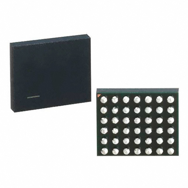
PACKAGE PHOTO
Rev. B
For more information www.analog.com
19
�LTC7150S/LTC7150S-4
PACKAGE DESCRIPTION
BGA Package
42-Lead (6mm
× 5mm × 1.30mm)
BGA Package
(Reference
DWG
# 05-08-1515
Rev C)
42-LeadADI
(6mm
× 5mm
× 1.30mm)
Z
(Reference LTC DWG # 05-08-1515 Rev C)
A1
2×
DETAIL A
A
ccc Z
6
A2
aaa Z
5
4
3
2
SEE NOTES
6
1
PIN 1
A
PIN “A1”
CORNER
b1
b
MOLD
CAP
4
B
C
SUBSTRATE
D
// bbb Z
H2
H1
E
DETAIL B
F
e
Øb (42 PLACES)
X
aaa Z
G
ddd M Z X Y
eee M Z
e
b
Y
E
2×
SEE NOTES
G
DETAIL B
PACKAGE SIDE VIEW
PACKAGE TOP VIEW
3
PACKAGE BOTTOM VIEW
NOTES:
1. DIMENSIONING AND TOLERANCING PER ASME Y14.5M-1994
DETAIL A
2. ALL DIMENSIONS ARE IN MILLIMETERS
2.0
1.2
0.4
0.4
1.2
2.0
0.000
DIMENSIONS
2.4
0.40 ±0.025 Ø 42x
1.6
0.8
0.000
0.8
1.6
2.4
SUGGESTED PCB LAYOUT
TOP VIEW
20
D
F
SYMBOL
A
A1
A2
b
b1
D
E
e
F
G
H1
H2
aaa
bbb
ccc
ddd
eee
MIN
1.10
0.30
0.80
0.45
0.37
NOM
1.30
0.40
0.90
0.50
0.40
6.00
5.00
0.80
4.80
4.00
0.20
0.70
MAX
1.50
0.50
1.00
0.55
0.43
NOTES
3
BALL DESIGNATION PER JEP95
4
DETAILS OF PIN #1 IDENTIFIER ARE OPTIONAL,
BUT MUST BE LOCATED WITHIN THE ZONE INDICATED.
THE PIN #1 IDENTIFIER MAY BE EITHER A MOLD OR
MARKED FEATURE
BALL HT
BALL DIMENSION
PAD DIMENSION
5. PRIMARY DATUM -Z- IS SEATING PLANE
6
!
PACKAGE ROW AND COLUMN LABELING MAY VARY
AMONG PRODUCTS. REVIEW EACH PACKAGE
LAYOUT CAREFULLY
SUBSTRATE THK
MOLD CAP HT
0.15
0.20
0.20
0.15
0.08
TOTAL NUMBER OF BALLS: 42
COMPONENT
PIN “A1”
TRAY PIN 1
BEVEL
PACKAGE IN TRAY LOADING ORIENTATION
BGA 42 0417 REV C
Rev. B
For more information www.analog.com
�LTC7150S/LTC7150S-4
REVISION HISTORY
REV
DATE
DESCRIPTION
A
12/17
Clarified conditions on top row of graphs
5
Clarified PGND
8
B
06/19
PAGE NUMBER
Clarified Block Diagram
9
Clarified Minimum Off-Time paragraph
12
Clarified Design Example inductor formula
18
Added LTC7150S-4 version
All
Added AEC-Q100 Qualified for Automotive Applications
1
EC Table – VFB, changed conditions from 125°C to 150°C
3
EC Table – Deleted Delta VFB (Line + Load)
3
EC Table – Added Delta Voltage Line Regulation and Load Regulation
3
EC Table – IFB, added Min spec
3
EC Table – UV, corrected Min and Max order (numbers unchanged)
3
EC Table – fOSC, Max changed from 1.1MHz to 1.15MHz
3
RDS(ON) vs Temperature, changed from 125°C max to 150°C max
5
PGOOD (Pin A2), FB pin description, changed from within ±7.5% to ±8%
8
Clarified capacitor between PVIN and PGND: 0.2µF – LTC7150S; 0.02µF – LTC7150S-4
9
Operation Section – corrected fourth paragraph ±7.5% to ±8%
10
Rev. B
Information furnished by Analog Devices is believed to be accurate and reliable. However, no responsibility is assumed by Analog
Devices for its use, nor for any infringements of patents or other rights of third parties that may result from its use. Specifications
Forgranted
morebyinformation
www.analog.com
subject to change without notice. No license is
implication or
otherwise under any patent or patent rights of Analog Devices.
21
�LTC7150S/LTC7150S-4
TYPICAL APPLICATION
3.3V/20A Step-Down Converter
0.33µH
VIN
4V TO 20V
22µF
×2
PVIN
SW
SVIN
FB
LTC7150S
RUN
CLKOUT
PGOOD
TRACK/SS
INTVCC
47µF
×2
10k
VOUT–
PHMODE
0.1µF
45.3k
VOUT
3.3V
20A
100µF
×2
MODE/SYNC
RT
GND
ITH
7150S TA03a
4.7µF
162k
10k
22pF
1nF
12VIN to –3.3VOUT 14A Step-Down Converter
0.33µH
12VIN
22µF
×2
PVIN
SW
SVIN
FB
LTC7150S
RUN
CLKOUT
MODE/SYNC
ITH
GND
RT
0.1µF
4.7µF
100µF
×2
–3.3VOUT
14A
PGOOD
TRACK/SS
0.1µF
47µF
×2
10k
VOUT–
PHMODE
INTVCC
45.3k
162k
10k
22pF
1nF
7150S TA03b
RELATED PARTS
PART NUMBER DESCRIPTION
COMMENTS
LTC3605/
LTC3605A
20V, 5A Synchronous Step-Down Regulator
4V < VIN < 20V, 0.6V < VOUT < 20V, 96% Maximum Efficiency,
4mm × 4mm QFN-24 Package
LTC3613
24V, 15A Monolithic Step-Down Regulator with
Differential Output Sensing
4.5V < VIN < 24V, 0.6V < VOUT < 5.5V, 0.67% Output Voltage Accuracy, Valley
Current Mode, Programmable from 200kHz to 1MHz, Current Sensing,
7mm × 9mm QFN-56 Package
LTC3622
17V, Dual 1A Synchronous Step-Down Regulator
with Ultralow Quiescent Current
2.7V < VIN < 17V, 0.6V < VOUT < VIN, 95% Maximum Efficiency,
3mm × 4mm DFN-14 and MSOP-16 Package
LTC3623
15V, ±5A Rail-to-Rail Synchronous Buck Regulator 4V ≤ VIN ≤ 15V, 96% Maximum Efficiency, 3mm × 5mm QFN Package
LTC3624
17V, 2A Synchronous Step-Down Regulator with
3.5µA Quiescent Current
2.7V < VIN < 17V, 0.6V < VOUT < VIN, 95% Maximum Efficiency, 3.5µA IQ,
Zero-Current Shutdown, 3mm × 3mm DFN-8 Package
LTC3633A/
LTC3633A-1
Dual Channel 3A, 20V Monolithic Synchronous
Step-Down Regulator
3.6V < VIN < 20V, 0.6V < VOUT < VIN, 95% Maximum Efficiency,
4mm × 5mm QFN-28 and TSSOP-28 Package
LTM4639
Low VIN 20A DC/DC µModule® Step-Down
Regulator
Complete 20A Switch Mode Power Supply, 2.375V < VIN < 7V, 0.6V < VOUT < 5.5V,
1.5% Maximum Total DC Output Voltage Error, Differential Remote Sense Amp,
15mm × 15mm BGA Package
LTM4637
20A DC/DC µModule Step-Down Regulator
Complete 20A Switch Mode Power Supply, 4.5V < VIN < 20V, 0.6V < VOUT < 5.5V,
1.5% Maximum Total DC Output Voltage Error, Differential Remote Sense Amp,
15mm × 15mm BGA or LGA Package
LTC7130
20V, 20A Monolithic Buck Converter with Ultralow 4.5V < VIN < 20V, 95% Maximum Efficiency, Optimized for Low Duty Cycle
DCR Sensing
Applications, 6.25mm × 7.5mm BGA Package
22
Rev. B
06/19
www.analog.com
For more information www.analog.com
ANALOG DEVICES, INC. 2017-2019
�


 工商网监
湘ICP备2023018690号
工商网监
湘ICP备2023018690号
