LTC7821
Hybrid Step-Down
Synchronous Controller
FEATURES
DESCRIPTION
Wide VIN Range: 10V to 72V (80V ABS Max)
nn Soft Switching for Low Noise Operation
nn Phase-Lockable Fixed Frequency 200kHz to 1.5MHz
nn ±1% Output Voltage Accuracy
nn R
SENSE or DCR Current Sensing
nn Programmable CCM, DCM, or Burst Mode® Operation
nn CLKOUT Pin for Multiphase Operation
nn Short Circuit Protected
nn EXTV
CC Input for Improved Efficiency
nn Monotonic Output Voltage Start-Up
nn Optional External Reference
nn 32-Pin (5mm × 5mm) QFN
The LTC®7821 uses a proprietary architecture that merges
a soft switching charge pump topology with a synchronous step-down converter to provide superior efficiency
and EMI performance compared to traditional switching
architectures.
APPLICATIONS
The LTC7821 can be easily paralleled to provide higher
output currents with its accurate current sharing capability
and frequency synchronization function.
nn
Intermediate Bus Converters
High Current Distributed Power Systems
nn Telecom, Datacom, and Storage Systems
nn Automotive Applications
nn
nn
In a typical 48V to 12V application, efficiency of greater
than 97% is attainable with the LTC7821 switching at
500kHz. The same efficiency can only be achieved with a
traditional controller switching at one-third the frequency.
Higher switching frequencies allow the use of smaller inductances that yield faster transient response and smaller
solution size.
All registered trademarks and trademarks are the property of their respective owners. Protected
by U.S. patents, Including 9484799.
TYPICAL APPLICATION
Efficiency at Various VIN for
VOUT = 12V
100Ω
1µF
VIN_SENSE
+
VIN
TG1
M1
VIN
36V TO 72V
2.2µF
×6
CIN
100µF
100
99
CB1, 0.22µF
BOOST1
LTC7821
FREQ
D1
M2
BG1
BOOST2
CB2
0.47µF
MID
EXT_REF
INTVCC
10k
MID_SENSE
CFLY
10µF
×8
FAULT
1k
PGOOD
PGOOD
PINS NOT SHOWN IN THIS CIRCUIT:
CLKOUT
TEMP
RUN
HYS_PRGM
MODE/PLLIN
TRACK/SS
4.32k
ITH
BOOST3
SW3
0.1µF
M3
TG2
D3
EXTVCC
VFB
93
30
40
50
60
INPUT VOLTAGE (V)
70
80
M4
6.81k
VOUT
12V
20A
0.22µF
10µF
×2
+
4.7µF
PGND
8V
fSW = 500KHz
VOUT = 12V
CCM
94
CMID
10µF
×8
2µH
INTVCC
INTVCC
96
7821 TA01b
CB3
1µF
BG2
IOUT = 20A
97
95
D2
10k
FAULT
EFFICIENCY (%)
SW1
TIMER
IOUT = 10A
98
COUT
150µF
×2
ISNS+
ISNS–
60.4k
7821 TA01a
M1: BSZ070N08LSS
M2, M3: BSC032N04LS
M4: BSC014N04LSI
Rev A
Document Feedback
For more information www.analog.com
1
�LTC7821
PIN CONFIGURATION
(Note 1)
ORDER INFORMATION
MID
MID_SENSE
VIN_SENSE
VIN
SW1
TG1
BOOST1
NC
TOP VIEW
32 31 30 29 28 27 26 25
MODE/PLLIN 1
24 BG1
CLKOUT 2
23 BOOST2
RUN 3
22 BOOST3
FAULT 4
21 TG2
33
SGND
PGOOD 5
20 SW3
TIMER 6
19 INTVCC
18 BG2
TRACK/SS 7
17 PGND
EXT_REF 8
EXTVCC
ISNS+
ISNS–
VFB
TEMP
ITH
9 10 11 12 13 14 15 16
HYS_PRGM
Input Supply Voltage (VIN, VIN_SENSE)........ –0.3V to 80V
Top Side Driver Voltages
BOOST1.................................................. –0.3V to 86V
BOOST2, BOOST3.................................. –0.3V to 46V
Switch Voltages
SW1............................................................. 0V to 80V
SW3........................................................ –0.3V to 40V
MID, MID_SENSE........................................ –0.3V to 40V
(BOOST1-SW1), (BOOST2-MID),
(BOOST3-SW3)............................................. –0.3V to 6V
ISNS+, ISNS –................................................. –0.3V to 40V
(ISNS+ – ISNS –)........................................................±0.6V
EXTVCC....................................................... –0.3V to 40V
TEMP, FREQ, EXT_REF, VFB................... –0.3V to INTVCC
HYS_PRGM, ITH, RUN, TRACK/SS........ –0.3V to INTVCC
FAULT, PGOOD............................................ –0.3V to 80V
TIMER, MODE/PLLIN............................. –0.3V to INTVCC
INTVCC Peak Output Current.................................100mA
Operating Junction Temperature Range
(Notes 2, 3, 9)..................................... –40°C to 125°C
Storage Temperature Range................... –65°C to 150°C
FREQ
ABSOLUTE MAXIMUM RATINGS
UH PACKAGE
32-LEAD (5mm × 5mm) PLASTIC QFN
TJMAX = 125°C, θJA = 44°C/W, θJC = 7.3°C/W
EXPOSED PAD (PIN 33) IS GND, MUST BE SOLDERED TO PCB
http://www.linear.com/product/LTC7821#orderinfo
LEAD FREE FINISH
TAPE AND REEL
PART MARKING*
PACKAGE DESCRIPTION
TEMPERATURE RANGE
LTC7821EUH#PBF
LTC7821EUH#TRPBF
7821
32-Lead (5mm × 5mm) Plastic QFN
–40°C to 125°C
LTC7821IUH#PBF
LTC7821IUH#TRPBF
7821
32-Lead (5mm × 5mm) Plastic QFN
–40°C to 125°C
Consult LTC Marketing for parts specified with wider operating temperature ranges. *The temperature grade is identified by a label on the shipping container.
For more information on lead free part marking, go to: http://www.linear.com/leadfree/
For more information on tape and reel specifications, go to: http://www.linear.com/tapeandreel. Some packages are available in 500 unit reels through
designated sales channels with #TRMPBF suffix.
Rev A
2
For more information www.analog.com
�LTC7821
ELECTRICAL CHARACTERISTICS
The l denotes the specifications which apply over the specified operating
junction temperature range, otherwise specifications are at TA = 25°C (Note 2). VIN = VIN_SENSE = 48V, VRUN = 5V, EXTVCC = 9V,
EXT_REF = 5.6V unless otherwise noted.
SYMBOL
PARAMETER
CONDITIONS
MIN
(Note 4)
0.9
TYP
MAX
UNITS
Main Control Loops
VIN
Input Voltage Range
10
Output Voltage Range
72
VIN
2
VFB
Regulated Feedback Voltage
ITH Voltage (Note 5)
IFB
Feedback Current
(Note 5)
VREFLNREG
Reference Voltage Line Regulation
VIN = 36V to 72V (Note 5)
VLOADREG
Output Voltage Load Regulation
(Note 5)
ΔITH Voltage = 1.2V to 0.7V
ΔITH Voltage = 1.2V to 1.6V
gm
Transconductance Amplifier gm
ITH = 1.2V; Sink/Source 5µA (Note 5)
IVIN
Input DC Supply Current
Normal Mode
Shutdown
Precharging Phase
(Note 6)
IVIN_SENSE
l
0.792
l
l
– 2.5
V
0.8
0.808
V
±10
±50
nA
0.003
0.02
%/V
0.016
–0.016
0.1
–0.1
%
%
2
VRUN = 0V, EXTVCC = 0V
VIN = 20V, VMID = VMID_SENSE = 9V,
VSW1 = 15V, VSW3 = 10V
VIN = 48V, VMID = VMID_SENSE = 20V,
VSW1 ≥ 36V, VSW3 = 12V
V
mmho
0.5
240
40
mA
µA
mA
84
mA
Input DC Supply Current
Normal Mode
Shutdown
(Note 6)
VRUN = 0V
1
45
mA
µA
IEXTVCC
Input DC Supply Current
(Note 6)
2.2
mA
IMID
MID Pin Current
45
μA
IMID_SENSE
MID_SENSE Pin Current
4
μA
VUVLO
VIN Undervoltage Lockout
VUVLO_HYST
UVLO Hysteresis
VSENSE
Current Sense Threshold
VISNS– = 0V
l
ISNS+/-
ISNS+ and ISNS– Pin Current
VISNS+ = VISNS– = 12V
l
ITRACK/SS
Soft-Start Charge Current
VTRACK/SS = 0V
VRUN_ON
RUN Pin On Threshold
VRUN Rising
IRUN
RUN Pin Current
VRUN = 0V
VRUN_HYST
RUN Pin Hysteresis
VEXT_REF_UC
EXT_REF Upper Clamp Limit
(Note 5)
l
VEXT_REF_LC
EXT_REF Lower Clamp Limit
(Note 5)
l
VSEL_EXT_REF
EXT_REF De-Select Threshold (Ramping Up)
IEXT_REF
EXT_REF Pin Current
VTEMP_TRIP
TEMP Pin Trip Point, Rising
VIN Ramping Up
8.8
l
9.4
0.28
l
45
50
55
mV
1.2
μA
–9
–10
–11
μA
1.1
1.3
1.6
0.85
μA
0.1
V
0.9
0.40
V
0.45
VTEMP_TRIP_HYST
TEMP Pin Trip Point Hysteresis
ITEMP
TEMP Pin Current
VTEMP = 1V
VBSTUVLO
Undervoltage Lockout of (BOOST1-SW1),
(BOOST2- VMID) and (BOOST3-SW3)
Difference Voltage, Rising
VBSTUVLO_HYST
TOUT
V
V
–150
l
V
1
1.3
VEXT_REF = 0.6V
V
V
nA
1.22
1.25
V
100
mV
1
nA
4.4
V
Bootstrap Undervoltage Lockout Hysteresis
1.4
V
TEMP Trip TimeOut
100
ms
Rev A
For more information www.analog.com
3
�LTC7821
ELECTRICAL CHARACTERISTICS
The l denotes the specifications which apply over the specified operating
junction temperature range, otherwise specifications are at TA = 25°C (Note 2). VIN = VIN_SENSE = 48V, VRUN = 5V, EXTVCC = 9V,
EXT_REF = 5.6V unless otherwise noted.
SYMBOL
PARAMETER
CONDITIONS
MIN
5.65
TYP
MAX
UNITS
5.8
5.95
V
–0.6
–2
%
INTVCC Linear Regulator
VINTVCC
Internal VCC Regulator
10V < VIN < 72V, VEXTVCC = 0V
VLDOINT
INTVCC Load Regulation
ICC = 1mA to 50mA, VIN = 12V, VEXTVCC = 0V
VEXTVCC
EXTVCC Switchover Voltage
EXTVCC Ramping Positive, ICC = 1mA
VEXTVCC_HYS
EXTVCC Switchover Voltage Hysteresis
VLDOEXT
EXTVCC Load Regulation
7
V
200
VEXTVCC = 12V, ICC = 1mA to 50mA
mV
–0.6
–2
%
Oscillator and Phase Lock Loop
fNOM
Nominal Frequency
RFREQ = 68kΩ
440
490
550
kHz
fLOW
Lowest Frequency
VFREQ = 0V
20
50
100
kHz
VFREQ = INTVCC
1400
1700
2000
kHz
fHIGH
Highest Frequency
fSYNC_LOW
Lowest Synchronizing Frequency
fSYNC_HIGH
Highest Synchronizing Frequency
200
kHz
1500
VFREQ = 0V
IFREQ
Frequency Setting Current
RMODE/PLLIN
MODE/PLLIN Resistance
250
kΩ
CLKOUTHIGH
CLKOUT High Amplitude
2.4
V
CLKOUTLOW
CLKOUT Low Amplitude
0
V
l
–9
–10
–11
KHz
µA
PGOOD Output
VPG1
PGOOD 1st Trip Level (with Delay)
VFB with Respect to Regulated Voltage
VFB Ramping Up (Overvoltage 1st Level)
VFB Ramping Down (Undervoltage 1st
Level)
VPG1_HYST
PGOOD 1st Trip Level Hysteresis (with Delay)
VPG2
PGOOD 2nd Trip Level
6
–5.5
8.5
–7.5
11
–9.5
%
%
15
mV
VFB with Respect to Regulated Voltage
VFB Ramping Up (Overvoltage 2nd Level)
VFB Ramping Down (Undervoltage 2nd
Level)
15
–25
%
%
0.4
VPG2_HYST
PGOOD 2nd Trip Level Hysteresis
VPGL
PGOOD Voltage Low
IPGOOD = 0.6mA
15
IPGOOD
PGOOD Leakage Current
VPGOOD = 80V
mV
0.5
V
1
μA
Capacitor Balancing
VTIMER_LOW
Voltage At TIMER Pin To Start Capacitor
Balancing
0.5
V
VTIMER_HIGH
Voltage At TIMER Pin To Stop Capacitor
Balancing
1.25
V
ITIMER
TIMER Pin Charge Current
VTIMER = 0.9V
VTIMER = 2.8V
VHYS_PRGM
Capacitor Balancing Window Comparator
Threshold
VHYS_PRGM = 0V
VHYS_PRGM = 1.2V
VHYS_PRGM = INTVCC
IHYS_PRGM
HYS_PRGM Pin Current
VHYS_PRGM = 0V
VFAULT
FAULT Pin Voltage Low
IFAULT = 0.6mA
IFAULT
FAULT Leakage Current
VFAULT = 80V
l
l
–6
–3
–7
–3.5
–8
–4
±0.3
±1.2
±0.8
l
–9
µA
µA
V
V
V
–10
–11
μA
0.2
0.4
V
1
μA
Rev A
4
For more information www.analog.com
�LTC7821
ELECTRICAL CHARACTERISTICS
The l denotes the specifications which apply over the specified operating
junction temperature range, otherwise specifications are at TA = 25°C (Note 2). VIN = VIN_SENSE = 48V, VRUN = 5V, EXTVCC = 9V,
EXT_REF = 5.6V unless otherwise noted.
SYMBOL
PARAMETER
CONDITIONS
MIN
TYP
MAX
UNITS
IFLYSRC1
Current Out of SW1 During Capacitor
Balancing
(VSW1 – VSW3) < VIN/2, VSW3 = 12V
40
mA
IFLYSNK1
Current into SW1 During Capacitor Balancing (VSW1 – VSW3) > VIN/2, VSW3 = 12V
Current into SW3 During Capacitor Balancing (VSW1 – VSW3) < VIN/2, VSW3 = 12V
6
mA
40
mA
IFLYSRC3
Current Out of SW3 During Capacitor
Balancing
(VSW1 – VSW3) < VIN/2, VSW3 = 12V
6
mA
IMID_SRC
Current Out of MID During Capacitor
Balancing
VMID < VIN/2, VMID = VMID_SENSE = 20V
VSW1 ≥ 36V, VSW3 = 12V
60
mA
IMID_SNK
Current into MID During Capacitor Balancing VMID > VIN/2, VMID = VMID_SENSE = 28V
VSW1 ≥ 36V, VSW3 = 12V
40
mA
TG1,2
Pull-Up ON Resistance
Pull-Down ON Resistance
2
1
Ω
Ω
BG1, 2
Pull-Up ON Resistance
Pull-Down ON Resistance
2
1
Ω
Ω
TG1,2 tr
TG1,2 tf
TG1, TG2 Transition Time:
Rise Time
Fall Time
(Note 7)
4
4
ns
ns
BG1,2 tr
BG1,2 tf
BG1, BG2 Transition Time:
Rise Time
Fall Time
(Note 7)
4
4
ns
ns
T1D
TG1 Off to BG1 On
45
ns
T2D
TG2 Off to BG2 On
20
ns
T3D
TG1 Off to TG2 Off
25
ns
T4D
BG1 Off to TG1 On
40
ns
T5D
BG2 Off to TG2 On
20
ns
T6D
BG1 Off to BG2 Off
20
ns
ton(MIN)
Minimum On-Time
210
ns
IFLYSNK3
Gate Driver
(Note 8)
Note 1: Stresses beyond those listed under Absolute Maximum Ratings
may cause permanent damage to the device. Exposure to any Absolute
Maximum Rating condition for extended periods may affect device
reliability and lifetime.
Note 2: The LTC7821E is guaranteed to meet performance specifications
from 0°C to 85°C. Specifications over the –40°C to 125°C operating
junction temperature range are assured by design, characterization and
correlation with statistical process controls. The LTC7821I is guaranteed
to meet performance specifications over the full –40°C to 125°C operating
junction temperature range. Note that the maximum ambient temperature
consistent with these specifications is determined by specific operating
conditions in conjunction with board layout, the rated package thermal
impedance and other environmental factors.
Note 3: TJ is calculated from the ambient temperature TA and power
dissipation PD according to the following formulas:
LTC7821UH: TJ = TA + (PD • 44°C/W)
Note 4: Output voltage range is guaranteed by design. For output voltage
setting, read “Output Voltage Setting” and “Minimum VOUT” in the
“Applications Information” section.
Note 5: The LTC7821 is tested in a feedback loop that servos VITH to a
specified voltage and measures the resultant VFB.
Note 6: Dynamic supply current is higher due to the gate charge being
delivered at the switching frequency. See Applications Information.
Note 7: Rise and fall times are measured using 10% and 90% levels. Delay
times are measured using 50% levels.
Note 8: The minimum on-time condition is specified for an inductor
peak-to-peak ripple current ≥ 40% of IMAX (see Minimum On-Time
Considerations in the Applications Information section)
Note 9: This IC includes overtemperature protection that is intended
to protect the device during momentary overload conditions. Junction
temperature will exceed 125°C when overtemperature protection is active.
Continuous operation above the specified maximum junction temperature
may impair device reliability or permanently damage the device.
Rev A
For more information www.analog.com
5
�LTC7821
TYPICAL PERFORMANCE CHARACTERISTICS
Efficiency at Various VIN
for VOUT = 12V
Efficiency and Power Loss
In Different Modes vs Load Current
100
8
100
90
7
99
4
fOSC = 500kHz
VIN = 48V
VOUT = 12V
60
50
3
CCM
DCM
BURST
30
0.1
1
10
LOAD CURRENT (A)
LTC7821 Start-Up Characteristic
(Pre-Balancing Period)
VIN
50V/DIV
TIMER
1V/DIV
PAGE 1
SCHEMATIC
IOUT = 20A
97
SW1 TO SW3
20V/DIV
96
MID
20V/DIV
95
2
40
IOUT = 10A
98
EFFICIENCY (%)
5
70
POWER LOSS (W)
EFFICIENCY (%)
6
PAGE 1
SCHEMATIC
80
TA = 25°C, unless otherwise noted.
1
94
0
100
93
fSW = 500KHz
VOUT = 12V
CCM
30
40
50
60
INPUT VOLTAGE (V)
70
100ms/DIV
7821 G02
80
7821 G02
7821 G01
Shutdown Current vs Temperature
LTC7821 Start-Up Characteristic
Quiescent Current vs Temperature
400
1.2
1.1
FAULT
5V/DIV
300
PGOOD
5V/DIV
VOUT
10V/DIV
100ms/DIV
7821 G03
IVIN_SENSE
1.0
SUPPLY CURRENT (mA)
350
IVIN (µA)
VIN
50V/DIV
250
200
0.9
0.8
0.7
0.6
IVIN
0.5
0.4
0.3
150
–50
–25
0
25
50
75
TEMPERATURE (°C)
100
0.2
–50
125
–25
0
25
50
75
TEMPERATURE (°C)
100
7821 G05
1.35
10.3
10.2
VIN (V)
RISING
1.25
FALLING
1.20
PIN CURRENT (µA)
8.8
1.30
VRUN (V)
HYS_PRGM, TRACK/SS and FREQ
Pin Current vs Temperature
9.0
1.40
RISING
8.6
8.4
FALLING
8.2
1.15
1.10
–50
7821 G06
Input Voltage UVLO Threshold
vs Temperature
Shutdown (RUN) Threshold
vs Temperature
–25
0
25
50
75
TEMPERATURE (°C)
100
125
7821 G07
125
10.1
HYS_PRGM Pin
10.0
TRACK/SS Pin
9.9
FREQ Pin
9.8
9.7
8.0
–50
–25
0
25
50
75
TEMPERATURE (°C)
100
125
7821 G08
9.6
–50
–25
0
25
50
75
TEMPERATURE (°C)
100
125
7821 G09
Rev A
6
For more information www.analog.com
�LTC7821
TYPICAL PERFORMANCE CHARACTERISTICS
TIMER Pin Current vs Temperature
TA = 25°C, unless otherwise noted.
Regulated Feedback Voltage
vs Temperature
TEMP Pin Current vs Temperature
7.5
804
10
7.0
VTIMER = 0V
6.5
803
1
5.0
4.5
0.1
VFB (mV)
802
5.5
ITEMP (nA)
ITIMER (µA)
6.0
VTEMP = 1V
0.01
800
4.0
3.5
0.001
VTIMER = 2.8V
3.0
2.5
–50
–25
0
25
50
75
TEMPERATURE (°C)
100
125
799
0.0001
–50
–25
0
25
50
75
TEMPERATURE (°C)
7821 G10
FREQUENCY (kHz)
599.60
600
800
575
700
525
500
475
450
599.30
425
EXT_REF = 0.6V
0
25
50
75
TEMPERATURE (°C)
100
400
125
0
10
20
6.50
30 40 50 60
INPUT VOLTAGE (V)
70
1200.0
0
0.5
1
1.5
2
FREQ PIN VOLTAGE (V)
2.5
7821 G16
0
–50
RFREQ = 68kΩ
–25
0
25
50
75
TEMPERATURE (°C)
100
5.75
5.00
6
10
14
18 22 26 30
EXTVCC VOLTAGE (V)
125
7821 G15
60
5.25
0
100
Current Sense Threshold
vs ITH Voltage
5.50
200.0
200
INTVCC Line Regulation
(Supply from EXTVCC)
6.00
400.0
300
80
6.25
1400.0
VINTVCC (V)
SWITCHING FREQUENCY (kHz)
1600.0
600.0
400
CURRENT SENSE THRESHOLD (mV)
1800.0
125
500
7821 G14
Switching Frequency
vs Voltage at FREQ Pin
800.0
100
600
RFREQ = 68kΩ
7821 G13
1000.0
0
25
50
75
TEMPERATURE (°C)
Oscillator Frequency
vs Temperature
550
599.90
EXT_REF = INTVCC
–25
7821 G12
OSCILLATOR FREQUENCY (kHz)
600.20
–25
798
–50
125
Oscillator Frequency
vs Input Voltage
600.50
VFB (mV)
100
7821 G11
Regulated Feedback Voltage
vs Temperature
599.00
–50
801
34
38
7821 G17
50
40
30
20
10
0
–10
–20
–30
0
0.4
0.8
1.2
ITH VOLTAGE (V)
1.6
2
7821 G18
Rev A
For more information www.analog.com
7
�LTC7821
TYPICAL PERFORMANCE CHARACTERISTICS
Maximum Current Sense Threshold
vs Common Mode Voltage
Voltage at Timer Pin to Start and
Stop Capacitor Balancing
vs Temperature
HYS_PRGM Voltage Window
vs Temperature
1.5
1.5
55.0
1.2
1.3
0.9
50.0
47.5
0.6
VHYS_PRGM = 1.2V
0.3
0.0
VHYS_PRGM = INTVCC
–0.3
0.9
0.7
–0.6
–0.9
Start Balancing
0.5
–1.2
45.0
0
5
10 15 20 25 30 35
VSENSE COMMON MODE VOLTAGE (V)
–1.5
–50
40
–25
0
25
50
75
TEMPERATURE (°C)
100
125
TEMP Pin Trip Voltage
vs Temperature
PULSESKIPPING
MODE
100mV/DIV
AC-COUPLED
Burst Mode
OPERATION
100mV/DIV
AC-COUPLED
VIN
10V/DIV
1.25
RISING
1.20
MID
10V/DIV
FALLING
VOUT
100mV/DIV
AC-COUPLED
1.10
1ms/DIV
1.05
1.00
–50
–25
0
25
50
75
TEMPERATURE (°C)
100
–25
0
25
50
75
TEMPERATURE (°C)
100
125
7821 G21
Line Transient 10V/ms
1.30
1.15
0.3
–50
7821 G20
7821 G19
VTEMP (V)
Stop Balancing
1.1
VTIMER (V)
52.5
VMID_SNS - VIN/2 (v)
CURRENT SENSE THRESHOLD (mV)
TA = 25°C, unless otherwise noted.
Steady-State Output Voltage
Ripple of Typical Application
CONTINUOUS
MODE
100mV/DIV
AC-COUPLED
7821 G23
VIN = 48V
VOUT = 12V
ILOAD = 30mA
125
10µs/DIV
7821 G24
7821 G22
Load Transient 2A–12A–2A of
Typical Application
Short-Circuit and Recovery
TEMP Fault Characteristic
TEMP
2V/DIV
VOUT
10V/DIV
IL
10A/DIV
SW3
20V/DIV
FAULT
10V/DIV
IL
20A/DIV
VOUT
500mV/DIV
AC-COUPLED
PGOOD
5V/DIV
PGOOD
5V/DIV
VIN = 48V
VOUT = 12V
f SW = 500kHz
50µs/DIV
7821 G25
VOUT
20V/DIV
200ms/DIV
7821 G26
20ms/DIV
7821 G27
Rev A
8
For more information www.analog.com
�LTC7821
PIN FUNCTIONS
MODE/PLLIN (Pin 1): Mode Selection or External Synchronization Input to Phase Detector. When external synchronization is not used, this pin selects the operating modes
and can be tied to SGND, to INTVCC or left floating. If the
pin is connected to SGND, it enables forced continuous
mode while a connection to INTVCC enables pulse-skipping
mode. Floating the pin enables Burst Mode operation.
For external sync, apply a clock signal to this pin. The
integrated PLL along with its internal compensation network will synchronize the internal oscillator to this clock.
Forced continuous mode will be enabled.
CLKOUT (Pin 2): Clock Output Pin. This pin outputs a
clock 180° out of phase with the main operating clock of
the LTC7821.
RUN (Pin 3): Run Control Input. A voltage above 1.3V
turns the controller ON. There is a 1μA pull-up current
on this pin when its voltage is below 1.3V.
FAULT (Pin 4): Open Drain Output pin. When the signal
goes low, it indicates one of the following conditions:
(a) In the capacitor balancing phase, capacitors CFLY or
CMID (see Typical Application) are not charged to
VIN/2. A low FAULT indicates an abnormal condition
that is preventing CFLY or CMID from being be charged
up to VIN/2.
(b) During normal operation, the voltage deviates from
VIN/2 by a window amount set by the voltage on the
HYS_PRGM pin.
(c) The die temperature exceeds its internally set limit or
the PTC resistor connected as the lower leg of a resistor
divider trips the TEMP pin threshold.
During any of these condition, the TRACK/SS pin will also
be pulled low.
PGOOD (Pin 5): Power Good Pin. This is an open drain
output. PGOOD is pulled to ground when the voltage of
the VFB pin is not within ±7.5% of its set point after an
internal 50μs mask timer expires. It will also be pulled low
when FAULT is tripped.
TIMER (Pin 6): Charge Balancing Timer Input. A capacitor connected from this pin to ground sets the amount
of time allocated to charge CFLY and CMID to VIN/2 during
the capacitor balancing phase. It also sets the auto-retry
timeout, should the capacitors fail to reach this voltage
within the set time. Capacitors CFLY and CMID begin and
end charging when the TIMER voltage is between 0.5V
and 1.2V, respectively. If the capacitor is balanced before
the TIMER voltage reaches 1.2V, this voltage is reset to
ground and normal operation begins. However, if the balance is not reached when the voltage reaches 1.2V, then
the charging of the capacitors stops and the auto-retry
timeout period begins. The TIMER capacitor will now slew
at half the rate until it reaches 4V and then resets to zero
and begins to slew at 1x rate. Once it reaches 0.5V, the CFLY
and CMID begin to charge again and the process repeats.
TRACK/SS (Pin 7): Output Voltage Tracking and Soft-Start
Input. The LTC7821 regulates the VFB voltage to the lowest
of three voltages: 0.8V, the voltage on the EXT_REF pin or
the voltage on the TRACK/SS pin. An internal 10μA pullup current source is connected to this pin. A capacitor to
ground at this pin sets the ramp time to the final regulated
output voltage. Alternatively, a resistor divider from another
voltage supply connected to this pin allows the LTC7821
output voltage to track the other supply during start-up.
EXT_REF (Pin 8): External Reference Input. A voltage applied to this pin forces the VFB to regulate to this voltage.
Internal clamps set at 0.4V and 0.93V limit the lower and
upper bounds of VFB regulation. Connecting this pin to
INTVCC will cause the internal reference to be used for
output voltage regulation.
HYS_PRGM (Pin 9): There is a 10μA current flowing out
of this pin. A voltage created by connecting a resistor
from this pin to ground sets an equal amount of window
threshold around VIN/2 to a window comparator. When the
voltage at MIDSENSE is not within this window threshold,
FAULT will be pulled low and switching will stop. CFLY and
CMID will be rebalanced to half of VIN before resuming
normal operation.
ITH (Pin 10): Current Control Threshold and Error Amplifier
Compensation Point. The current comparator threshold
increases with its ITH control voltage.
FREQ (Pin 11): Frequency Set Pin. There is a 10μA current
flowing out of this pin. A resistor to ground sets a voltage
which in turn programs the frequency.
Rev A
For more information www.analog.com
9
�LTC7821
PIN FUNCTIONS
TEMP (Pin 12): Temperature Sensing Input. Using a PTC
resistor as the lower leg of a resistor divider, connect the
TEMP pin to the common point of the divider. The PTC
resistor is used to monitor a hot spot on the PCB. Once
it reaches the TEMP threshold of 1.22V, the LTC7821
stops switching for 100ms before retrying. Ground this
pin if not used.
TG2 (Pin 21): Floating Gate Drive for Second Lowermost
N-Channel MOSFET. The voltage swings equal to INTVCC
superimposed on the switch node voltage SW3.
VFB (Pin 13): Error Amplifier Feedback Input. This pin
receives the remotely sensed feedback voltage from an
external resistive divider across the output.
BOOST1, BOOST2, BOOST3 (Pin 31, 23, 22): Bootstrapped
Supplies to Floating Drivers. Capacitors are connected
between the BOOSTx and SWx (MID) pin. Voltage swing
at the BOOST1 pin is from (VIN/2 + INTVCC) to (VIN + INTVCC). Voltage at the BOOST2 pin is at (VIN/2 + INTVCC).
Voltage swing at the BOOST3 pin is from INTVCC to (VIN/2
+ INTVCC).
ISNS– (Pin 14): Current Sense Comparator Input. The (–)
input to the current comparator is Kelvin connected to the
output voltage of the controller.
BG1 (Pin 24): Floating Gate Drive for Second Uppermost
N-Channel MOSFET. The voltage swings between (VIN/2
+ INTVCC) and VIN/2.
ISNS+ (Pin 15): Current Sense Comparator Input. The (+)
input to the current comparator is normally Kelvin connected to the DCR sensing networks or current sensing
resistor.
MID (Pin 25): Half Supply from VIN. Do not use this to
source current. Connect a bypass capacitor from this
node to PGND.
EXTVCC (Pin 16): External Power Input to an Internal LDO
Connected to INTVCC. This LDO supplies INTVCC power,
bypassing the internal LDO powered from VIN whenever
EXTVCC is higher than 6.4V. Do not float or exceed 40V
on this pin.
PGND (Pin 17): Driver Power Ground. Connect this pin
closely to the source of bottom (synchronous) N-channel
MOSFET M4, the (–) terminal of CIN and the (–) terminal
of CVCC.
BG2 (Pin 18): Gate Drive for the Bottom (synchronous)
N-Channel MOSFET. The voltage swings from slightly
below ground to INTVCC.
INTVCC (Pin 19): Internal Regulator Output. The bottom
synchronous gate driver and control circuits are powered
from this regulator. Bypass this pin to PGND with a minimum
of 4.7μF low ESR tantalum or ceramic capacitor. Do not
use the INTVCC pin for any purpose other than described
in this data sheet.
SW3 (Pin 20): Switch Node Connection to Inductor and
One Terminal of Flying Capacitor. Voltage swing at this pin
is from slightly below ground to VIN/2.
MIDSENSE (Pin 26): Half Supply Monitor. Provides Kelvin
sensing input for the comparator that monitors the voltage
between MIDSENSE and ground. An RC filter can be added
from MID to this pin to filter out noise.
VIN_SENSE (Pin 27): VIN Kelvin Sensing Input. Allows an
internal VIN/2 to be generated for LTC7821 control circuit
usage. For a cleaner supply, an RC filter can be added
from VIN to this pin.
VIN (Pin 28): Main Input Supply. Bypass this pin to PGND
with a capacitor.
SW1 (Pin 29): Switch Node Connection to One Terminal
of Flying Capacitor. Voltage swing at this pin is from VIN/2
voltage to VIN.
TG1 (Pin 30): Floating Gate Drive for Uppermost N-Channel
MOSFET. The voltage swings equal to INTVCC superimposed
on the switch node voltage SW1.
SGND (Exposed Pad, Pin 33): Signal Ground. All Smallsignal components and compensation components should
connect to this ground, which in turn connects to PGND
at one point. Exposed pad must be soldered to the PCB,
providing a local ground for the control components of
the IC, and be tied to the PGND pin under the IC.
Rev A
10
For more information www.analog.com
�LTC7821
BLOCK DIAGRAM
MODE/PLLIN
VIN_SENSE
BOOST1
500k
MODE/SYNC
DETECT
C3
S
SW1
BOOST2
–
R2
TG1
BST CAP
CHARGER
1.5M
VIN
C2
BG1
BST CAP
CHARGER
+
0.6V
MID
Q
SLOPE
COMP
R
3k
+
FCNT
IREV
–
–
BURSTEN
SWITCH
LOGIC
AND
ANTI-SHOOT
THROUGH
+
ICMP
ITH
1.5M
VIN/2
PLL SYNC
OSC
INTVCC
500k
FREQ
CLKOUT
VIN
1
51k
VIN
BOOST3
BST CAP
CHARGER
TG2
SW3
INTVCC
RUN
BG2
PGND
SNS–
SNS+
VIN/2
3.5µA
+
3.5µA
1.2V
CAPACITOR
BALANCING
CIRCUIT
–
BALEN
+
TIMER
0.5V
4V
BAL
BALEN
–
TEMP
+
10µA
MID_SENSE
FAULT
+
–
100ms
TIMEOUT
–
1.2V
EXTVCC
6.48V
EA
INTVCC
+
V/I
HYS_PRGM
VIN
–
0.8VREF
+
+
–
SHDN
1.2V
SHDN
EXT
LINEAR
REG
INT
LINEAR
REG
R1
10µA
+
TRACK/SS
1.2V
SLEEP
R4
–
0.86V
1µA
+
×1.075
+
–
+
SS
+
–
0.5V
RUN
–
×0.925
x0.825
1.2V
VA
VB
OV
0.74V
–
PGOOD
VC
0.66V
+
7821 BD01
UV
–
RUN
EXT_REF
VFB
Rev A
For more information www.analog.com
11
�LTC7821
OPERATION
Capacitor Balancing Phase
During normal operation, only CMID is monitored for deviation away from VIN/2 by a window amount set by a resistor
connected from HYS_PRGM to ground. The voltage across
this resistor sets the same amount of window threshold
above and below VIN/2. If VCMID leaves this voltage window, all switching will stop and the TRACK/SS pin will be
pulled low. Corresponding internal current sources will be
turned on to bring CFLY and CMID voltages back to VIN/2.
FAULT will be pulled low and released once the balancing
is complete. During this balancing period, PGOOD will
also be pulled low. The TRACK/SS pin is also allowed to
charge up upon the completion of balancing. Connecting
HYS_PRGM to INTVCC sets the window threshold to ±0.8V
around VIN/2. (see Figure 2)
During initial power up, the voltage across the flying capacitor (CFLY) and CMID are measured. If either of these voltages
are not at VIN/2, the TIMER’s capacitor will be allowed to
charge up. When the TIMER capacitor’s voltage reaches
0.5V, internal current sources to bring CFLY voltage to VIN/2
are turned ON. After the CFLY voltage has reached VIN/2,
CMID will then be charged to VIN/2. The TRACK/SS pin is
pulled low during this duration and all external MOSFETs
are shut off. The FAULT pin will not be pulled low during
this initial power up. If the voltages across CFLY and CMID
reach VIN/2 before the TIMER capacitor’s voltage reaches
1.2V, the TRACK/SS will be released and allowed to charge
up. The TIMER pin will reset to ground and remain there.
Normal operation will begin (see Figure 1A).
Main Control Loop
If, however, the CFLY or CMID voltage is not at VIN/2 when
VTIMER reaches 1.2V, the internal current sources will be
turned OFF and the TIMER capacitor will be charged at half
the initial rate until it reaches 4V. Timer will then be reset
to zero, and the LTC7821 will repeat the above process
again until CFLY and CMID are at VIN/2(See Figure 1B).
FAULT
Once the capacitor balancing phase is completed, normal
operation begins. MOSFETs M1 and M3 are turned ON
when the clock sets the RS latch, and turned off when
the main current comparator, ICMP, resets the RS latch.
MOSFETs M2 and M4 are then turned on. The peak inductor
FAULT
0V
0V
4V
TIMER
1.2V
0.5V
TIMER
TRACK/SS
1.2V
0.5V
TRACK/SS
(B)
(A)
7821 F01
Figure 1. Charge Balancing During Power Up with (A) Balancing Completed within One Timer Period and
(B) More Than One Timer Period
FAULT
TIMER
FAULT
1.2V
0.5V
TIMER
1.2V
0.5V
TRACK/SS
TRACK/SS
(A)
(B)
7821 F02
Figure 2. Charge Balancing During Normal Operation with (A) Balancing Completed within One Timer Period and
(B) More Than One Timer Period
Rev A
12
For more information www.analog.com
�LTC7821
OPERATION
current at which ICMP resets the RS latch is controlled by
the voltage on the ITH pin, which is the output of the error
amplifier EA. The VFB pin receives the voltage feedback
signal, which is compared to the internal reference voltage
by the EA. When the load current increases, it causes a
slight decrease in VFB relative to the 0.8V reference, which
in turn causes the ITH voltage to increase until the average inductor current matches the new load current. After
MOSFETs M1 and M3 have turned OFF, MOSFETs M2 and
M4 are turned ON until either the inductor current starts
to reverse, as indicated by the reverse current comparator
IREV, or the beginning of the next cycle.
During the switching of M1/M3 and M2/M4, capacitor
CFLY is alternately connected in series with or parallel to
CMID. The voltage at MID will be approximately at VIN/2.
INTVCC/EXTVCC Power
Power for the bootstrap drivers and bottom MOSFET and
most internal circuitry is derived from the INTVCC pin. When
the EXTVCC pin is grounded or tied to a voltage less than
7V, an internal 5.8V linear regulator supplies INTVCC power
from VIN. If EXTVCC is taken above 7V, this linear regulator is turned OFF and another 5.8V linear regulator turns
ON to provide the INTVCC power from EXTVCC. Using the
EXTVCC pin allows the INTVCC power to be derived from
a high efficiency external source, resulting in an overall
increase in system efficiency.
Bootstrap Capacitor Refresh
Each of the three uppermost MOSFET drivers is biased
from its respective floating bootstrap capacitor, CB1 to
CB3, which are refreshed during switching through a
charge pump configuration consisting of diodes D1 to
D3 and the external MOSFETs.
During the charge balancing phase or light load condition
when switching may stop for extended amount of time,
the voltage across the bootstrap capacitor may decrease
sufficiently that the gate drive voltage is not optimal. Undervoltage detectors monitor the voltage across each of
the bootstrap capacitors. When any of them goes below
3V, an internal current source of 1mA will be turned ON
to charge that bootstrap capacitor through the upper plate
of the capacitor. A 1mA sinking source that is connected
to the bottom plate of the bootstrap capacitor will also be
turned ON to sink away this current. This ensures a net
zero residual current at the bottom plate capacitor node,
hence avoiding any impact on the bias condition of that
node. When CB1 and CB2/CB3 reach 4.3V and 4.47V
respectively, the refreshing stops. When CB2 and CB3
need to be refreshed, all switching stops.
Shutdown and Start-Up (RUN and TRACK/SS Pins)
When the RUN pin is below 1.3V, the INTVCC linear regulator
along with all the internal circuitry that is powered from
this supply, is disabled. The main control loop will also
be disabled. Releasing the RUN pin will allow the internal
1μA current source to pull this pin up, thus enabling the
part. The RUN pin can also be driven directly by logic but
ensure that this voltage does not exceed the Absolute
Maximum Rating of 6V.
The slew rate of the output voltage VOUT can be controlled
by the voltage on the TRACK/SS pin. When the voltage
on the TRACK/SS is less than the internal reference of
0.8V (or EXT_REF if this feature is invoked), the LTC7821
regulates the VFB voltage to the TRACK/SS voltage instead
of to the reference. This allows the TRACK/SS pin to be
used to program the soft-start period by connecting an
external capacitor from the TRACK/SS pin to SGND. An
internal 10μA pull-up current charges this capacitor, creating a voltage ramp on the TRACK/SS pin. As the TRACK/
SS voltage rises linearly from 0V to the reference voltage
(and beyond), the output voltage VOUT rises smoothly
from zero to the final value. Alternatively, the TRACK/SS
pin can be used to cause the start-up of VOUT to track that
of another supply. Typically this requires connecting to the
TRACK/SS pin an external resistor divider from the other
supply to ground (see Application Information section).
Light Load Current Operation (Burst Mode Operation,
Pulse-Skipping Mode, or Continuous Conduction)
The LTC7821 can be enabled to enter high efficiency Burst
Mode operation, constant-frequency pulse-skipping mode,
or forced continuous conduction mode. To select forced
continuous operation, tie the MODE/PLLIN pin to a DC
voltage below 0.6V (e.g., SGND). To select pulse-skipping
mode of operation, tie the MODE/PLLIN pin to INTVCC. To
select Burst Mode operation, float the MODE/PLLIN pin.
Rev A
For more information www.analog.com
13
�LTC7821
OPERATION
When the controller is enabled for Burst Mode operation,
the peak current in the inductor is set to approximately
one-third of the maximum sense voltage even though
the voltage on the ITH pin indicates a lower value. If the
average inductor current is higher than the load current,
the error amplifier output, EA, will decrease the voltage
on the ITH pin. When the ITH voltage drops below 0.5V,
the internal sleep signal goes high (enabling sleep mode)
and all external MOSFETs are turned off. In sleep mode,
the load current is supplied by the output capacitor. As the
output voltage decreases, the EA’s output begins to rise.
When the output voltage drops enough, the sleep signal
goes low, and the controller resumes normal operation by
turning on the external MOSFETs on the next cycle of the
internal oscillator. When a controller is enabled for Burst
Mode operation, the inductor current is not allowed to
reverse. The reverse current comparator (IREV) turns off
the bottom external MOSFET M4 and M2 just before the
inductor current reaches zero, preventing it from reversing and going negative. Thus, the controller operates in
discontinuous operation.
In forced continuous operation, the inductor current is
allowed to reverse at light loads or under large transient
conditions. The peak inductor current is determined by
the voltage on the ITH pin. In this mode, the efficiency at
light loads is lower than in Burst Mode operation. However,
continuous mode has the advantages of lower output ripple
and less interference with audio circuitry.
When the MODE/PLLIN pin is connected to INTVCC, the
LTC7821 operates in PWM pulse-skipping mode at light
loads. At very light loads, the current comparator ICMP
may remain tripped for several cycles and force the external
MOSFETs M1 and M3 to stay off for the same number of
cycles (i.e., skipping pulses). The inductor current is not
allowed to reverse (discontinuous operation). This mode,
like forced continuous operation, exhibits low output ripple
as well as low audio noise and reduced RF interference
as compared to Burst Mode operation. It provides higher
low current efficiency than forced continuous mode, but
not nearly as high as Burst Mode operation.
Frequency Selection and Phase-Locked Loop (FREQ
and MODE/PLLIN Pins)
The selection of switching frequency is a trade-off between
efficiency and component size. Low frequency operation
increases efficiency by reducing MOSFET switching losses,
but requires larger inductance and/or output capacitance
to maintain low output ripple voltage. In addition, it will
also require larger BOOST capacitance and balancing capacitance (CFLY and CMID) since the refresh rate is lower.
The switching frequency of the LTC7821’s controller can
be selected using the FREQ pin. If the MODE/PLLIN pin
is not being driven by an external clock source, the FREQ
pin can be used to program the controller’s operating
frequency from 50kHz to 1.7MHz.
There is a 10µA current flowing out of the FREQ pin, so
the user can program the controller’s switching frequency
with a single resistor to SGND.
A phase-locked loop (PLL) is integrated on the LTC7821
to synchronize the internal oscillator to an external clock
source that is connected to the MODE/PLLIN pin. The
controller operates in forced continuous mode when it is
synchronized. The PLL loop filter network is integrated
inside the LTC7821. The phase-locked loop is capable
of locking any frequency within the range of 200kHz to
1.5MHz. The frequency setting resistor should always be
present to set the controller’s initial switching frequency
before locking to the external clock.
Temperature Monitoring
When the LTC7821 die temperature reaches 150°C,
switching stops and TRACK/SS pin is pulled low. Charge
balancing is also disabled.
The LTC7821 can provide hotspot monitoring via the
TEMP pin. By using a PTC thermistor as the lower leg of a
resistor divider and connecting the common point of this
divider to the TEMP pin, the voltage increases drastically
when the temperature reaches beyond the Curie point of
the PTC thermistor as shown in Figure 3. The characteristic of the PTC thermistor is shown in Figure 4. When the
TEMP pin reaches 1.22V, all switching stops for 100ms.
Rev A
14
For more information www.analog.com
�LTC7821
OPERATION
The temperature that is use to trigger the hotspot protection will determine the thermistor selection. This temperature will be the Curie point of the thermistor, which is
often defined as having two times its resistance at 25°C.
With the Curie point resistance of the thermistor known,
R2CURIE, the upper resistance, R1, can be selected by the
following equation:
R1=
R2CURIE (V EXT – 1.22)
1.22
Power Good (PGOOD Pin)
When VFB pin voltage is not within ±10% of the internal
0.8V reference or the reference set by EXT_REF, the PGOOD
pin is pulled low. The PGOOD pin is also pulled low when
the RUN pin is below 1.3V or when the LTC7821 is in the
VEXT
soft-start or tracking phase. The PGOOD pin will flag power
good immediately when the VFB pin is within the ±10% of
the reference window. However, there is an internal 50µs
power bad mask when VFB goes out the ±10% window.
The PGOOD pin is allowed to be pulled up by an external
resistor to sources of up to 80V.
FAULT (FAULT Pin)
During initial power up of the LTC7821 or when enabling
the part via the RUN pin, the FAULT pin will not be pulled
low even when CFLY and/or CMID needed to be rebalanced
to VIN/2. But during normal operation, when rebalancing
is needed, the FAULT will be pulled low. Another condition
that causes the FAULT to go low is thermal shutdown, either
caused by the internal die temperature reaching 150°C or
the voltage at TEMP pin reaching 1.22V. The FAULT pin is
allowed to be pulled up by an external resistor to sources
of up to 80V.
RESISTANCE OF THERMISTOR (LOG Ω)
The voltage on the TRACK/SS pin and FAULT is pulled low
and is released after 100ms (Figure 5) if the voltage on the
TEMP pin goes below 1.1V during this 100ms timeout.
If the TEMP pin voltage remains above 1.1V, the timeout
period will be extended until the voltage drops below 1.1V.
LTC7821
R1
TEMP
CURIE POINT
25°C
TEMPERATURE OF THERMISTOR (°C)
PTC
R2
7821 F04
Figure 4. Characteristic of a Thermistor
7821 F03
Figure 3. Temperature Monitoring Setup
TEMP
TEMP TRIP LEVEL = 1.22V
SWx
100ms
TRACK/SS
FAULT
7821 F05
Figure 5. Temperature Trip Characteristic
For more information www.analog.com
Rev A
15
�LTC7821
APPLICATIONS INFORMATION
The “Typical Application” on the first page is a basic
LTC7821 application circuit. The LTC7821 can be configured to use either DCR (inductor resistance) sensing
or resistor sensing. The choice between the two current
sensing schemes is largely a design trade-off between
cost, power consumption, and accuracy. DCR sensing is
popular because it saves an expensive current sensing
resistor and is more power efficient, especially in high
current applications. However, a current sensing resistor
provides the most accurate current limit for the application.
Other external component selection is driven by the load
requirement, and begins with the selection of RSENSE (if
RSENSE is used). Next CFLY, CMID, and the power MOSFETs
are selected, followed by the input and output capacitors.
In addition to the power level, switching frequency plays
a role in selecting the balancing capacitance (CFLY and
CMID) and the inductance of the inductor.
ISNS+ and ISNS– Pins
The ISNS+ and ISNS– pins are the inputs to the current
comparators. The common mode input voltage range of
the current comparators is 0V to 36V. Both ISNS pins are
high impedance inputs with small leakage currents of less
than 1.2µA. When the ISNS pins ramp up from 0V to 2.4V,
small base currents flow out of the ISNS pins. When the
ISNS pins ramp down from 36V to 2V, the small base currents flow into the ISNS pins. The high impedance inputs
to the current comparators allow accurate DCR sensing.
However, care must be taken not to float these pins during
normal operation.
Filter components mutual to the sense lines should be
placed close to the LTC7821, and the sense lines should
run close together to a Kelvin connection underneath the
current sense element (shown in Figure 6). Sensing current elsewhere can effectively add parasitic inductance
and capacitance to the current sense element, degrading
the information at the sense terminals and making the
programmed current limit unpredictable. If DCR sensing
is used (Figure 7b), sense resistor R1 should be placed
close to the switching node, to prevent noise from coupling
into sensitive small-signal nodes. The capacitor C1 should
be placed close to the IC pins.
TO SENSE FILTER,
NEXT TO THE CONTROLLER
C OUT
R SENSE
7821 F06
Figure 6. Sense Lines Placement with Sense Resistor
Resistor Current Sensing
The hybrid architecture of the LTC7821 generates a voltage
rail of half the VIN supply to the step-down control loop.
Therefore the current ripple calculation and its operating
duty cycle is referred to the voltage at the MID pin which
is approximately at VIN/2.
A typical sensing circuit using a discrete resistor is shown
in Figure 7a. RSENSE is chosen based on the required
output current.
The current comparator has a maximum threshold of
50mV and its inputs have a common mode range of 0V
to 36V. The current comparator threshold sets the peak of
the inductor current, yielding a maximum average output
current IMAX equal to the peak value less half the peak-topeak ripple current, ∆IL. To calculate the sense resistor
value, use the equation:
R SENSE =
50mV
ΔI
I(MAX ) + L
2
Because of possible PCB noise in the current sensing
loop, the AC current sensing ripple of ∆VSENSE = ∆IL •
RSENSE also needs to be verified in the design to get a
good signal-to-noise ratio.
In general, for a reasonably good PCB layout, a 10mV
∆VSENSE voltage is recommended as a conservative number
to start with, either for RSENSE or DCR sensing applications,
for duty cycles less than 40%. For applications where
the inductor’s ripple current could be greater than 50%
and operating at 750kHz and above, the sense resistor’s
parasitic inductance has to be taken into consideration
since its contribution is no longer negligible.
Rev A
16
For more information www.analog.com
�LTC7821
APPLICATIONS INFORMATION
INTVCC
INTVCC
MID
R
MID_SENSE
C
BOOST3
L
SW3
M4
BG2
PGND
ISNS+
RF
CF
ISNS–
RS
ESL
CF • 2RF < ESL/RS
POLE-ZERO
CANCELLATION
INDUCTOR
C
BOOST3
L
SW3
COUT
C1
7821 F07a
COUT
PLACE R1 NEXT
TO INDUCTOR
ISNS+
RF
VOUT
R1
PGND
ISNS–
DCR
M4
BG2
FILTER COMPONENTS
PLACED NEAR SENSE PINS
(7a) USING A RESISTOR TO SENSE CURRENT
M3
TG2
VOUT
C
C
C
D
SENSE RESISTOR
PLUS PARASITIC
INDUCTANCE
M3
TG2
R
MID_SENSE
C
C
D
MID
C
R2
PLACE C1 NEAR
SNS+, SNS– PINS
(7b) USING INDUCTOR DCR TO SENSE CURRENT
7821 F07b
Figure 7. Two Different Methods of Sensing Current
In an application where the sense resistor’s parasitic inductance contribution is negligible, a small RC filter placed
near the IC is enough to reduce the effects of capacitive
and inductive noise coupled in the sense traces on the
PCB. A typical filter consists of two series 10Ω resistors
connected to a parallel 1000pF capacitor, resulting in a
time constant of 20ns. However, the same RC filter with
minor modifications can be used to extract the resistive
component of the current sense signal in the presence
of significant parasitic inductance in the sense resistor.
For example, Figure 8 illustrates the voltage waveform
across a 1mΩ sense resistor with a 2010 footprint for the
12V/20A converter operating at 100% load. The waveform
is the superposition of a purely resistive component and a
purely inductive component. It was measured using two
scope probes and waveform math to obtain a differential
measurement. Based on additional measurements of the
inductor ripple current and the on-time and off-time of
the top switch, the value of the parasitic inductance was
determined to be 0.3nH using the equation:
Check the sense resistor manufacturer’s data sheet for
information about parasitic inductance. In the absence of
data, measure the voltage drop directly across the sense
resistor to extract the magnitude of the ESL step and use
VSENSE
5mV/DIV
500ns/DIV
7821 F08
Figure 8. Voltage Waveform Measured Directly
Across the Sense Resistor
VSENSE
5mV/DIV
⎛ t •t
⎞
V
ESL = ESL(STEP) • ⎜ ON OFF ⎟
⎝ t ON + t OFF ⎠
ΔIL
If the RC time constant is chosen to be close to the parasitic
inductance divided by the sense resistor (L/R), the resulting waveform looks resistive again, as shown in Figure 9.
500ns/DIV
7821 F09
Figure 9. Voltage Waveform Measured After the
Sense Resistor Filter, CF = 1nF, RF = 100Ω
For more information www.analog.com
Rev A
17
�LTC7821
APPLICATIONS INFORMATION
the equation to determine the ESL. However, do not over
filter. Keep the RC time constant less than or equal to the
inductor time constant to maintain a high enough ripple
voltage on VRSENSE. The filter components need to be
placed close to the IC. The positive and negative sense
traces need to be routed as a differential pair and Kelvin
connected to the sense resistor.
20°C. Increase this value to account for the temperature
coefficient of resistance, which is approximately 0.4%/°C.
A conservative value for TL(MAX) is 100°C. To scale the
maximum inductor DCR to the desired sense resistor
value, use the divider ratio:
Inductor DCR Sensing
For applications requiring the highest possible efficiency
at high load currents, the LTC7821 is capable of sensing
the voltage drop across the inductor DCR, as shown in
Figure 7b. The DCR of the inductor represents the small
amount of DC winding resistance of the copper, which
can be less than 1mΩ for today’s low value, high current
inductors. In a high current application requiring such an
inductor, conduction loss through a sense resistor would
cost several points of efficiency compared to DCR sensing.
RD =
R SENSE(EQUIV )
DCR(MAX) AT T L(MAX )
C1 is usually selected to be in the range of 0.047µF to
0.47µF. This forces R1|| R2 to around 2kΩ, reducing error
that might have been caused by the SENSE pins’ 1.2µA
current. TL(MAX) is the maximum inductor temperature.
The equivalent resistance R1||R2 is scaled to the room
temperature inductance and maximum DCR:
R1||R2 =
L
(DCR AT 20°C) • C1
If the external R1|| R2 • C1 time constant is chosen to be
exactly equal to the L/DCR time constant, the voltage drop
across the external capacitor is equal to the drop across
the inductor DCR multiplied by R2/(R1 + R2). R2 scales the
voltage across the sense terminals for applications where
the DCR is greater than the target sense resistor value.
To properly dimension the external filter components, the
DCR of the inductor must be known. It can be measured
using a good RLC meter, but the DCR tolerance is not
always the same and varies with temperature; consult
the manufacturers’ data sheets for detailed information.
The sense resistor values are:
Using the inductor ripple current value from the Inductor
Value Calculation section, the target sense resistor value is:
where VMID is half the voltage of VIN.
R SENSE(EQUIV ) =
50mV
ΔI
I(MAX ) + L
2
To ensure that the application will deliver full load current
over the full operating temperature range, choose the
minimum value for the Maximum Current Sense Threshold
(VSENSE(MAX)) in the Electrical Characteristics table.
Next, determine the DCR of the inductor. Where provided,
use the manufacturer’s maximum value, usually given at
R1=
R1||R2
RD
;
R2 =
R1• R D
1– R D
The maximum power loss in R1 is related to duty cycle,
and will occur in continuous mode at the maximum input
voltage:
P LOSS _ R1 =
( VMID – VOUT ) • VOUT
R1
Ensure that R1 has a power rating higher than this value.
If high efficiency is necessary at light loads, consider this
power loss when deciding whether to use DCR sensing or
sense resistors. Light load power loss can be modestly
higher with a DCR network than with a sense resistor, due
to the extra switching losses incurred through R1. However,
DCR sensing eliminates a sense resistor, reduces conduction losses and provides higher efficiency at heavy loads.
Peak efficiency is about the same with either method.
To maintain a good signal to noise ratio for the current
sense signal, use a minimum ∆VSENSE of 10mV for duty
Rev A
18
For more information www.analog.com
�LTC7821
APPLICATIONS INFORMATION
cycles less than 40%. For a DCR sensing application, the
actual ripple voltage will be determined by the equation:
V
V OUT
–V
Δ V SENSE = MID OUT •
R1• C1
V MID • fOSC
and because a lower limit is placed on the inductor value
to avoid subharmonic oscillations. To ensure stability for
duty cycles up to the maximum of 95%, use the following
equation to find the minimum inductance.
L MIN >
Slope Compensation and Inductor Peak Current
Slope compensation provides stability in constant frequency architectures by preventing subharmonic oscillations at high duty cycles. It is accomplished internally by
adding a compensating ramp to the inductor current signal
at duty cycles in excess of 40%. Normally, this results in
a reduction of maximum inductor peak current for duty
cycles >40%. However, the LTC7821 uses a scheme that
counteracts this compensating ramp, which allows the
maximum inductor peak current to remain unaffected
throughout all duty cycles.
where
Inductor Value Calculation
Given the desired input and output voltages, the inductor
value and operating frequency fOSC directly determine the
inductor’s peak-to-peak ripple current:
V
V
–V
IRIPPLE = OUT • MID OUT
V MID
fOSC • L
Lower ripple current reduces core losses in the inductor,
ESR losses in the output capacitors, and output voltage
ripple. Thus, highest efficiency operation is obtained at
low frequency with a small ripple current. Achieving this,
however, requires a large inductor.
A reasonable starting point is to choose a ripple current
that is about 40% of IOUT(MAX) for a duty cycle less than
40%. Note that the largest ripple current occurs at the
highest input voltage. To guarantee that ripple current does
not exceed a specified maximum, the inductor should be
chosen according to:
L≥
V MID – V OUT
V
• OUT
fOSC • IRIPPLE V MID
For duty cycles greater than 40%, the 10mV current
sense ripple voltage requirement is relaxed because the
slope compensation signal aids the signal-to-noise ratio
V OUT
fSW • ILOAD(MAX )
• 1.4
LMIN is in units of µH
fSW is in units of MHz
Inductor Core Selection
Once the inductance value is determined, the type of inductor must be selected. Core loss is independent of core
size for a fixed inductor value, but it is very dependent on
inductance selected. As inductance increases, core losses
go down. Unfortunately, increased inductance requires
more turns of wire and therefore copper losses will increase.
Ferrite designs have very low core loss and are preferred
at high switching frequencies, so design goals can concentrate on copper loss and preventing saturation. Ferrite
core material saturates hard, which means that inductance collapses abruptly when the peak design current is
exceeded. This results in an abrupt increase in inductor
ripple current and consequent output voltage ripple. Do
not allow the core to saturate!
Power MOSFET Selection
Four external power MOSFETs must be selected for the
LTC7821. The gate drive voltages to these MOSFETs are
derived from the INTVCC voltage, which is typically 5.8V.
Hence logic-level threshold MOSFETs must be selected.
Only the upper-most MOSFET requires a BVDSS greater
than VIN, because this MOSFET sees the full VIN voltage
during start-up. The other MOSFETs, M2 to M4, need only
have a BVDSS greater than VIN/2.
During operation, the type of switching also impacts how
each power MOSFET is selected. M1 and M2 operate in
soft switching mode, so they should have low Qoss •
Rev A
For more information www.analog.com
19
�LTC7821
APPLICATIONS INFORMATION
MOSFET input capacitance is a combination of several
components but can be taken from the typical gate charge
curve included on most data sheets (see Figure 10). The
curve is generated by forcing a constant input current into
the gate of a common source, current source loaded stage
and then plotting the gate voltage versus time.
The initial slope is the effect of the gate-to-source and
the gate-to-drain capacitance. The flat portion of the
curve is the result of the Miller multiplication effect of the
VIN
MILLER
EFFECT
VGS
+
–
a
V
b
+
–
+
QIN
CMILLER = (QB – QA)/VDS
VGS
VDS
–
7821 F10
Figure 10. Gate Change Characteristic
gate-to-drain capacitance as the drain drops the voltage
across the current source load. The upper sloping line is
due to the drain-to-gate accumulation capacitance and
the gate-to-source capacitance. The Miller charge (the
increase in coulombs on the horizontal axis from a-to-b
while the curve is flat) is specified for a given VDS drain
M3
M3 CURRENT FLOW
L1
M4
M4 CURRENT FLOW
C1
voltage, but can be adjusted for different VDS voltage by
multiplying the ratio of the application VDS to the curve
specified VDS value. A way to estimate the CMILLER term is
to take the change in gate charge from point a-and-b on a
manufacturer’s data sheet and divide by the specified VDS
voltage. CMILLER is the most important selection criteria
for determining the transition loss term in the MOSFET
M3 but is not directly specified on MOSFET data sheets.
CRSS and COss are specified sometimes but definitions of
these parameters are not included.
In a traditional synchronous buck converter, the current
flowing through the upper and lower MOSFET is the same
as the inductor current (see Figure 11). In the hybrid topology of the LTC7821, the MOSFET and inductor currents
do not match, because the capacitors play a role in energy
transfer to the output.
In the first phase (see Figure 12a), M1 and M3 are ON
and the capacitor CMID provides part of the inductor current via M3. The rest of the inductor’s current is provided
through CFLY via M1. If the capacitance of CFLY is the same
as CMID, then the inductor’s current is equally supplied
by both capacitors as shown in Figure 12b. Therefore
compared to the traditional buck converter with the same
amount of inductor current, less current flowing through
M3 means lower switching loss and conduction loss. Since
M3 switches hard, this reduction in current reduces the
switching loss significantly.
In the 2nd phase, M2 and M4 are ON (see Figure 13a).
In this phase, M4 not only has to supply the full inductor
INDUCTOR CURRENT
RdsON product. M3 and M4 operate in a manner similar
to traditional buck converter, with M3 hard switching while
M4 operates in zero voltage switching (ZVS). Therefore M3
and M4 should be chosen with the lowest (Qgd • RdsON)
and (Qg • RdsON) product, respectively.
M3 CURRENT
M4 CURRENT
TIME
7821 F11
Figure 11. MOSFET’s Current of Traditional Synchronous Buck Converter
Rev A
20
For more information www.analog.com
�LTC7821
APPLICATIONS INFORMATION
M1
M2
iL
CFLY
INDUCTOR CURRENT
CURRENT
M3
L1
CMID
1/2iL
M1 AND M3 CURRENT
IF C FLY = CMID
C1
M4
TIME
(12a) CURRENT PATH OF M1 AND M3
7821 F12
(12b) M1 AND M3 CURRENT MAGNITUDE
Figure 12. First Phase M1 and M3 Current Flow
M1
M2
C FLY
CURRENT
M4 CURRENT
M3
L1
CMID
INDUCTOR CURRENT
M2 CURRENT
C1
M4
TIME
(13a) CURRENT PATH OF M2 AND M4
7821 F13
(13b) M2 AND M4 CURRENT MAGNITUDE
Figure 13. Second Phase M2 and M4 Current Flow
Rev A
For more information www.analog.com
21
�LTC7821
APPLICATIONS INFORMATION
current, but also carries the balancing current that flows
between CFLY and CMID due to an imbalance of voltage
between the two capacitors at the end of phase 1. Therefore M4 has an increase in conduction losses compared
to its counterpart in a traditional buck converter. The
current flowing through M2 is dependent on the voltage
differential between the capacitors, their ESR, RDSON of
M2 and M4, and inductance of the MOSFETs, capacitors,
and board traces (see Figure 13b).
When the controller is operating in continuous mode the
duty cycles for M1, M3, M2 and M4 are given by:
2 • V OUT
M1, M3 Switch Duty Cycle =
V IN
V – 2 • V OUT
M2, M4 Switch Duty Cycle = IN
V IN
The power dissipation of M1 and M3 is given by:
⎛I
⎞ 2 ⎛ 2 • V OUT ⎞
•C
P M1 = ⎜ MAX FLY ⎟ ⎜
⎟ ( 1+ d ) R DS(ON)
⎝ C FLY + C MID ⎠ ⎝ V IN ⎠
⎛I
⎞ 2 ⎛ 2 • V OUT ⎞
•C
P M3 = ⎜ MAX MID ⎟ ⎜
⎟ ( 1+ d ) R DS(ON) +
⎝ C FLY + C MID ⎠ ⎝ V IN ⎠
⎛ V IN ⎞ 2 ⎛ IMAX • C MID ⎞
(R DR ) ( CMILLER ) •
⎜⎝
⎟
2 ⎠ ⎜⎝ 2 • ( C FLY + C MID ) ⎟⎠
1
1
⎡
⎤
+
⎢V
⎥•f
⎣ INTVCC – VTH(MIN) VTH(MIN) ⎦
where d is the temperature dependency of RDS(ON), RDR
is the effective top driver resistance (approximately 2Ω
at VGS = VMILLER), and VIN is the input supply. VTH(MIN)
is the data sheet specified typical gate threshold voltage
specified in the power MOSFET data sheet at the specified
drain current. CMILLER is the calculated capacitance using
the gate charge curve from the MOSFET data sheet and
the technique described above.
If the switching loss contribution of PM3 is relatively small
compared to its conduction loss, then the overall power
dissipation (PM1 + PM3) will be the lowest when CFLY = CMID.
The power dissipation of M2 and M4 is harder to calculate, because the current flowing through these MOSFETs
exhibits a 2nd order system response due to the presence
of parasitic package inductance of the MOSFETs and capacitors, ESR of the capacitors, RDS(ON) of the MOSFETs
and the capacitance of CMID and CFLY. Complicating the
matter is that the current could exhibit overdamped, critically damped or underdamped characteristics, depending
on the RLC values mentioned above; this would impact
the RMS current significantly. Use ADI/LTC power tool to
help select M2 and M4.
With the RMS current flowing through M2 and M4 determined, the power dissipation is given by:
P M2 = I2rms2 • ( 1+ d ) R DS(ON)
P
= I2
• ( 1+ d ) R
DS(ON)
M4 rms4
CFLY and CMID Selection
In this hybrid topology, capacitors CFLY and CMID are part of
the energy transfer elements. Therefore ceramic capacitors
are attractive since they have the lowest ESR. However,
care should be taken when choosing this type of capacitor.
During operation the DC voltage across the CFLY and CMID
is approximately half the VIN supply, therefore the voltage
rating of the capacitors should be greater than that. As
a general rule, select the voltage rating of the capacitor
to be twice the operating voltage of the capacitor. For the
same voltage rating and capacitance, a larger case size
will have a lower failure rate.
In addition, the operating temperature of the capacitors
needs to be considered. For operating temperature above
85°C, capacitors with the X7R dielectric need to be used
while X5R dielectric is adequate for operation below 85°C.
For long term reliability of the capacitor, keep the temperature rise of the capacitor to be below 20°C, preferably
10°C. The temperature rise of the capacitor is dependent
on the amount of RMS current through the capacitor and
the operating frequency. Consult the manufacturer’s data
sheet for this data.
Rev A
22
For more information www.analog.com
�LTC7821
APPLICATIONS INFORMATION
Ceramic capacitors also have a large voltage coefficient,
losing close to half their capacitance when the DC bias
across a given capacitor is half its rated voltage. The DC
bias effect on a capacitor is greater when the case size
is smaller. Factor in these effects when deciding on the
capacitance.
The ripple voltage of CFLY and CMID is given by:
As a good starting point, select enough capacitance such
that the ripple on each capacitor is less than 1% of the DC
bias voltage of the capacitor. For example, if the DC bias
voltage of the capacitor is 24V, keep the ripple to be less
than 240mV. For the lowest conduction loss of MOSFETs
M1 and M3 (see Power MOSFET Selection section), select
the capacitance of CMID to be the same as that of CFLY.
Schottky Diode and Bootstrap Capacitors Selection
I
•t
V CFLY _ RIPPLE = OUT ON
2 • C FLY
IOUT • t ON
V CMID _ RIPPLE =
2 • C MID
Three diodes are used to form a charge pump circuit
to provide the drive voltages for MOSFETs M1 to M3.
Figure 14 shows the diodes configuration. The voltages
across the following bootstrap capacitors are approximately:
where IOUT is the output current and tON is the on-time
of M1 and M3.
VBST1_SW1 = VINTVCC – VF_D1 – VF_D2 – VF_D3
The ripple voltage on CFLY and CMID, (VCFLY_RIPPLE, VCMID_
RIPPLE ), contributes significantly to the power dissipated
in M2 and M4 (see Power MOSFET Selection section).
VBST2_SW3 = VINTVCC – VF_D3
VBST2_MID = VINTVCC – VF_D2 – VF_D3
where VF_DX is the forward voltage of diode X.
D1
VIN
LTC7821
TG1
CBST1
M1
SW1
D2
BG1
M2
CBST2
MID
D3
TG2
CBST3
M3
SW3
INTVCC
BG2
M4
7821 F14
Figure 14. External Charge Pump
Rev A
For more information www.analog.com
23
�LTC7821
APPLICATIONS INFORMATION
To obtain the most translation in voltage from VINTVCC to
drive M1, Schottky diodes are recommended.
The reverse voltage seen by each of the Schottky diodes
is approximately:
V
V R _ DIODE ≅ IN
2
Pay attention to the leakage current when selecting the
forward drop of the diodes. In general, the lower the
forward drop for the same amount of current flowing
through the diode, the higher the leakage current. As
these diodes will be operating with large reverse bias for
high VIN applications, the leakages are higher, especially
at higher operating temperatures.
The charge pump diodes operate as conduits for transferring charge from one capacitor to another and as such are
subjected to transient current rather than a DC current.
Hence peak forward surge rating is more important than
the average current rating. A surge rating of 750mA is a
good starting point.
Since the bootstrap capacitor acts as a supply for the
MOSFET’s driver, select large enough capacitance so
that the voltage does not droop considerably when the
MOSFETs are being turned ON. As with the CMILLER estimation described in the Power Selection section, the user
can use the same graph to obtain the total gate charge for
a given gate drive voltage. This can then easily converted
to its equivalent gate capacitance by:
CG =
QG
V GS
If the bootstrap capacitor voltage is not allowed to droop
by more than 1%, then:
CBST ≥ 99CG
Besides acting as a supply for their respective MOSFET
drivers, CBST2 and CBST3 also serve as charge pump capacitors. As a good starting point, size CBST2 and CBST3
as follows:
CBST3 ≥ 2CBST2 ≥ 2CBST1
Soft-Start and Tracking
The LTC7821 has the ability to either soft-start by itself
with a capacitor or track the output of another channel or
external supply. When configured to soft-start by itself, a
capacitor should be connected to its TRACK/SS pin and
ground. When RUN pin voltage is below 1.22V, the TRACK/
SS is actively pulled to ground in this shutdown state.
Once the RUN pin voltage is above 1.22V, the controller
powers up and a soft-start current of 10µA begins to flow
out of the TRACK/SS pin. However, the TRACK/SS will start
charging its soft-start capacitor only after charge balance
is completed and the associated active pull-down of the
TRACK/SS is released. Note that soft-start or tracking is
achieved not by limiting the maximum output current of
the controller but by controlling the output ramp voltage
according to the ramp rate on the TRACK/SS pin. Current
fold-back is disabled during this phase to ensure smooth
soft-start or tracking. Depending on whether the EXT_REF
feature has been invoked or not, the soft-start or tracking
range is defined to be either the voltage range from 0V to
0.8V or 0V to VEXT_REF on the TRACK/SS pin. The total
soft-start time can be calculated as:
t SOFT − START = ( 0.8 or VEXT _ REF ) •
C SS
10µA
Regardless of the mode selected by the MODE/PLLIN pin,
the regulator will always start in pulse-skipping mode up
to TRACK/SS = 82.5% of 0.8V or VEXT_REF.
Output Voltage Tracking
The LTC7821 allows the user to program how its output
ramps up and down by means of the TRACK/SS pins.
Through this pin, the output can be set up to either coincidentally or ratio-metrically track another supply’s output,
as shown in Figure 15. In the following discussions, VOUT1
refers to another supply’s output (master channel) while
VOUT2 refers to the LTC7821 output (slave channel) that
tracks VOUT1. To implement the coincident tracking in Figure
15a, connect an additional resistive divider to VOUT1 and
connect its midpoint to the TRACK/SS pin of the LTC7821.
The ratio of this divider should be the same as that of the
slave channel’s feedback divider shown in Figure 16a. In
this tracking mode, VOUT1 must be set higher than VOUT2.
Rev A
24
For more information www.analog.com
�LTC7821
APPLICATIONS INFORMATION
VOUT1
OUTPUT VOLTAGE
OUTPUT VOLTAGE
VOUT1
VOUT2
VOUT2
TIME
TIME
(15a) COINCIDENT TRACKING
(15b) RATIO-METRIC TRACKING
7821 F15
Figure 15. Two Different Methods of Output Voltage Tracking
(FROM LTC7821)
VOUT1
EXTERNAL SUPPLY
VOUT2
R3
TO
TRACK/SS
PIN OF
LTC7821
R1
R3
TO
VFB1
PIN
R4
(FROM LTC7821)
VOUT1
TO
TRACK/SS
PIN OF
LTC7821
TO
VFB2
PIN
R4
R2
EXTERNAL SUPPLY
VOUT2
R3
R1
TO
VFB1
PIN
TO
VFB2
PIN
R2
(16a) COINCIDENT TRACKING SETUP
R4
(16b) RATIO-METRIC TRACKING SETUP
7821 F16
Figure 16. Setup for Coincident and Ratio-Metric Tracking
In order to track down another channel or supply after
the soft-start has successfully reached 82.5% of 0.8V
or VEXT_REF, it is recommended to set the LTC7821 into
force continuous mode operation by setting the MODE/
PLLIN = 0V. For no load condition, the LTC7821 should
be in force continuous mode to ensure good tracking of
the master supply.
By selecting different resistors, the LTC7821 can achieve
different modes of tracking including the two in Figure
15. The ratio-metric mode uses one less pair of resistors
compared to the coincident mode but has lesser output
accuracy on VOUT2 and is also fully coupled to any variations in VOUT1. In both modes, there is an error in output
voltage setting cause by the pin current of TRACK/SS. To
minimize this error, use smaller resistor values in the divider.
Output Voltage Setting
The LTC7821 uses its internal reference of 0.8V when the
VEXT_REF ≥ 1.3V. The output voltage is given by:
⎛ R2 ⎞
V OU T = 0.8 • ⎜ 1+
⎟
⎝
R1 ⎠
If the applied voltage to the EXT_REF is less than 1.3V,
then VOUT will track EXT_REF voltages between 0.4V and
0.9V, as indicated by the characteristic in Figure 17.
0.9•(1+R2/R1)
VOUT
To implement the ratiometric tracking in Figure 15b, the
ratio of the VOUT2 divider should be exactly the same as
the master channel’s feedback divider ratio shown in
Figure 16b.
0.4•(1+R2/R1)
0.4V
VEXT_REF
0.9V
7821 F17
Figure 17. Output Voltage Set By EXT_REF Pin
Rev A
For more information www.analog.com
25
�LTC7821
APPLICATIONS INFORMATION
Due to its unique architecture, the optimal efficiency for
the LTC7821 is when VOUT ≅ VIN/4. For applications that
demand optimal efficiency within a range of VIN, EXT_REF
could be used to track this VIN variation while maintaining
a 4:1 step down ratio at the output. In this type of setup
the output voltage will also change with the input. Figure
18 shows a 48V to 12V setup that accounts for VIN variation between 36V to 72V.
VIN
(36V TO 72V)
VOUT
(9V TO 18V)
R1
82.5K
R5
464k
R6
5.9k
TO
EXT_REF
PIN
TO
VFB
PIN
R2
4.32k
7821 F18
Figure 18. Output Voltage to Track VIN in 4:1 Ratio
The minimum output voltage that can be set for the LTC7821
is limited by the charge balancing circuit and its minimum
on-time. The charge balancing circuitry requires at least
2V on the output and is independent of VIN. The minimum
on time determines the minimum VOUT by:
V
•t
V OU T(MIN) = MID ON(MIN)
TS
Where TS is the switching period.
Hence,
V
•t
⎛
⎞
V OU T(MIN) = MAX ⎜ 2.5V, MID ON(MIN) ⎟
⎝
⎠
TS
V
V OU T(MAX ) = IN – 2.5
2
For applications where the load is resistive and acts like
a discharging path, the minimum VOUT can be lowered
to 0.8V.
26
During the CFLY capacitor balancing phase, a current of
approximately 40mA (ISRC) flows out of SW1 node to
charge the flying capacitor CFLY to VIN/2. To prevent this
current from charging COUT, an identical amount is sunk
(ISNK) away at SW3 node. Figure 21 shows the current
path. A minimum output voltage of 2V is needed to ensure
the complete sinking of the sourcing current.
In applications that need the output to be regulated below
2V, a resistive load can be added across VOUT to ensure
that the voltage will not exceed the regulated value during
the capacitor balancing phase. The resistive load value is
given by:
V
R LOAD < OUT
0.04
Select RLOAD to be about 70% of the calculated value.
HYS_PRGM Voltage
The voltage on the HYS_PRGM pin sets a window (threshold) centered on VIN/2 for fault protection purpose. During
operation, if the voltage across MID_SNS and ground deviates beyond this window, a fault is indicated and capacitor
balancing begins. Therefore setting the correct window
is important as it adds another layer of protection to the
power system. In continuous switching, the first order
approximate impedance at MID is given by:
D1• T
The internal charge balancing circuitry requires a minimum
differential voltage between VIN/2 and VOUT of 2.5V to operate. This limits the maximum output voltage setting to:
Minimum VOUT
–D1• T
–D2 • TS
D2 • TS
S
S
⎛
2 • t1
2
•
t1
2
•
t2
+e
+ e 2 • t2
⎜e
Z MID =
•
+ eD2 • T
–D1•
–D2 • TS
T
D1•
T
⎜
S
S
S
8 • C FLY • fSW
⎜⎝ 2 • t1
2
•
t2
2
•
t1
e
– e 2 • t2
e
–e
1
⎛
⎛ D1• TS ⎞
⎛ D2 • TS ⎞ ⎞
=
• ⎜ coth
+ coth
⎝ 2 • t1 ⎠
⎝ 2 • t2 ⎠ ⎟⎠
8 • C FLY • fSW ⎝
1
where:
TS = Switching period
fSW = Switching frequency
D1 = Duty cycle of MOSFET 1 and 3
D2 = Duty cycle of MOSFET 2 and 4
t1 = (RON1 + RON3 + RESR_FLY) • CFLY
t2 = (RON2 + RON4 + RESR_FLY) • CFLY
RONX = Resistance of MOSFET X in Ω
For more information www.analog.com
⎞
⎟
⎟
⎟⎠
Rev A
�LTC7821
APPLICATIONS INFORMATION
Figure 19a shows a typical LTC7821 output stage setup
while 19b shows the equivalent circuit. Note that M3 and
M4 form the buck converter switches, taking its power
from MID, with its voltage given by:
⎛
V
V
1⎞
V MID = IN – ⎜ IOUT • OUT • ⎟ • Z MID
2 ⎝
V IN h ⎠
M1, M3 DUTY CYCLE =
where h = efficiency of the buck converter.
A good conservative number to use for h is 0.9.
The above equation gives us the average MID voltage
and does not include the AC ripple on it. The CMID ripple
voltage is given by (see CFLY and CMID Selection section):
Since VIN = 48V, Infineon BSC027N06LS5 is chosen for
M1. This is an 60V MOSFET. For M2 to M4, 30V MOSFETs
are sufficient for this application. For M2 and M3, Infineon
BSC032N04LS are selected and an Infineon BSC014N04LSI
is selected for M4.
I
•t
V CMID _ RIPPLE = OUT ON
2C MID
Therefore the maximum deviation of MID voltage from
VIN/2 is given by:
= 0.208
24
T OFF = (1– 0.208) • 2µs = 1.58µs
With inductor current ripple initially scaled to 40% of
output current, ΔIL = 0.4 • 25 = 10A,
Design Example
A 48V to 5V, 25A operating at 500kHz application is used
as an example. Since the output current is high, DCR
sensing is used to regulate the current loop.
For 500kHz operation, a 68k resistor is connected from
FREQ to ground.
V OUT • T OFF
Hence, L =
ΔI L
=
5 • 1.58 • 10 – 6
10
= 0.79µH
An inductance of 0.9µH is selected (Coilcraft SER2011901L) instead and this give ΔIL = 8.8A. The RMS current
through the inductor is:
⎛
ΔI2L ⎞
IRMS _ L = ⎜I2OUT +
⎟
⎝
12 ⎠
V
I
•t
ΔV MID _ IDEAL = IN – V MID – OUT ON
2
2C MID
Use the above equation as a guideline to set the HYS_PRGM
voltage.
5
=
25 2 +
0.4 2
12
= 25.2A
From the manufacturer data sheet, the rise in temperature
of the inductor is 15°C. However, this rise does not account
for the conduction of heat from the MOSFETs through the
PCB that increases the overall inductor’s temperature.
Depending on how the board is being laid out and how
much air flow is applied, the net increase in temperature
could be higher. For this design example, assume the net
temperature rise to be 50°C.
The typical DCR of the inductor is typically 1.2mΩ with a
maximum of 1.34 mΩ and with a 50°C rise in temperature
and assuming the temperature coefficient of the DCR at
0.4%/°C, the maximum DCR is:
⎛ 0.4 • 50 ⎞
–3
R DCΔ = 15°C = 1.34 • ⎜ 1+
⎟ • 10
⎝
100 ⎠
= 1.61m Ω
Rev A
For more information www.analog.com
27
�LTC7821
APPLICATIONS INFORMATION
VIN
LTC7821
TG1
M1
SW1
CFLY
BG1
M2
MID_SNS
+
–
RFILT
MID
TG2
VIN
2
CFILT
CMID
V
M3
L
V
f(HYS_PRGM)
+
BG2
VOUT
RFB1
M4
COUT
–
RFB2
VFB
(19a) LTC7821 OUTPUT SETUP
LTC7821
MID_SNS
+
–
RFILT
MID
ZMID
CFILT
V1
VIN
2
VIN
2
V1
f(HYS_PRGM)
+
TG2
M3
L
CMID
BG2
VOUT
RFB1
M4
COUT
–
RFB2
VFB
7821 F19
(19b) LTC7821 THEVEVIN OUTPUT EQUIVALENT
Figure 19. LTC7821 Output Setup
Rev A
28
For more information www.analog.com
�LTC7821
APPLICATIONS INFORMATION
With a VSENSE = 50mV, the DCR will set the peak inductor
current to be 31A. With a ripple ΔIL of 8.8A, the application
will provide 25A of output current.
The next components to select are the bootstrap capacitors. For M1, the gate charge needed to charge its gate
from VGS = 0V to 6V is:
For the sensing network, select C1 = 0.22μF, then:
QG = 9nC
R8 =
Therefore, it’s equivalent gate capacitance is:
L
C1• DCR
= 3.4kΩ
CG =
QG
V GS
= 1.5nF
Hence, CBST1 = 99 • CG
For the design, a 3.32k resistor is used.
The next components to select are the CMID and CFLY. In
this example,
CMID = CFLY
CBST2 = 0.47μF
To maintain ripple at CMID and CFLY to be 1% of its
DC bias:
ΔV CMID and ΔV CFLY = 0.01• 24
= 240mV
I
•t
C FLY = OUT ON
2 • ΔV CMID
25 • 0.42 • 10 – 6
=
2 • 0.24
= 21.88µF
For the Schottky diodes, Central’s CMDSH-4 are used.
1
⎛
⎛ D1• T S ⎞
⎛ D2 • T S ⎞ ⎞
• ⎜ coth ⎜
+ coth ⎜
⎟
⎝ 2 • t1 ⎠
⎝ 2 • t2 ⎟⎠ ⎟⎠
8 • C FLY • f SW ⎝
= 18.15mΩ
This will result in an average MID voltage of:
VMID = VIN/2 – (31A • 18.15mΩ)
The voltage rating chosen for these capacitors is 50V
and even with this rating, the actual capacitance is lower
due to its voltage coefficient. 6 × 10µF is chosen for each
CMID and CFLY. With this value of CMID, the voltage ripple
at MID is now:
= 87.5mV
CBST3 = 1μF
Z MID =
= C MID
V CMID _ ripple =
Use, CBST1 = 0.22μF
From the manufacturer data sheet, the RDSON of M1 to
M4 are 3.1mΩ, 3.2mΩ, 3.2mΩ, and 1.4mΩ respectively.
The equivalent impedance at MID node, ZMID, can be
calculated to be:
Hence,
= 0.15μF
IOUT • t ON
2 • 60 • 10 – 6
= 23.437V
Factoring in the ripple voltage on CMID, the minimum
VMID is:
V MID _ MIN = 23.437 – 0.0875
= 23.35V
This is 650mV lower than the ideal voltage of 24V at MID
point. Therefore set the voltage at HYST_PRGM pin to be
1V with a resistor of 100k.
The completed circuit for this design example is shown
in Figure 20.
Rev A
For more information www.analog.com
29
�LTC7821
APPLICATIONS INFORMATION
Minimum On-Time Considerations
Minimum on-time tON(MIN) is the smallest time duration
that the LTC7821 is capable of turning on the top MOSFET.
It is determined by internal timing delays and the gate
charge required to turn on the top MOSFET. Low duty
cycle applications may approach this minimum on-time
limit and care should be taken to ensure that:
t ON(MIN) <
2 • V OUT
V IN(f)
If the duty cycle falls below what can be accommodated
by the minimum on-time, the controller will begin to skip
cycles. The output voltage will continue to be regulated,
but the ripple voltage and current will increase.
The minimum on-time for the LTC7821 is approximately
210ns, with reasonably good PCB layout, minimum 30%
inductor current ripple and at least 10mV – 15mV ripple
on the current sense signal. The minimum on-time can be
affected by PCB switching noise in the voltage and current
loop. As the peak sense voltage decreases the minimum
on-time increases. This is of particular concern in forced
continuous applications with low ripple current at light
loads. If the duty cycle drops below the minimum on-time
limit in this situation, a significant amount of cycle skipping can occur with correspondingly larger current and
voltage ripple.
Multiphase Operation
For high output power applications, two LTC7821's can be
paralleled to create a dual phase single output configuration. Figure 22 shows the key signal connections between
the two LTC7821s.
Rev A
30
For more information www.analog.com
�LTC7821
APPLICATIONS INFORMATION
100
10
97
9
94
8
91
7
88
6
85
5
82
79
3
VOUT = 5V
76
2
CCM
73
70
4
VIN = 48V
1
fSW = 500kHz
1
5
9
13
17
LOAD CURRENT (A)
POWER LOSS (W)
EFFICIENCY (%)
Efficiency and Power Loss for
48V to 5V vs Load Current
21
25
0
7821 F20a
R2, 1k
C1
0.1µF
VIN_SENSE
+
VIN
TG1
CBST1, 0.22µF
C6, 0.47µF
C7, 0.1µF
R6, 68k
R7, 100k
TEMP
SW1
TIMER
LTC7821
RUN
FREQ
HYS_PRGM
R4
10k
FAULT
CMDSH-4
BG1
BOOST2
MID_SENSE
PGOOD
MODE/PLLIN
ITH
C8
470pF
R1
6.04k
C9
1nF
TRACK/SS
C10
0.1µF
SW3
RFB2
4.32k
EXTVCC
VFB
CBST3, 1µF
C5
0.1µF
M3
BSC032N04LS
CMID
10µF
50V
×6
GRM32ER71H106KA12
1k
SER2011-901L
L1, 0.9µH
D3, CMDSH-4
INTVCC
PGND
8V
R3
BG2
INTVCC
CFLY
10µF
50V
×6
GRM32ER71H106KA12
D2
TG2
BOOST3
M2
BSC032N04LS
CBST2
0.47µF
CMDSH-4
FAULT
PGOOD
C4
2.2µF
100V
×6
D1
MID
R5
10k
CIN
100µF
100V
BOOST1
EXT_REF
INTVCC
M1
BSC027N06LS5
VIN
48V
M4
BSC014N04LSI
R8, 3.3k
C11
0.22µF
C3
10µF
+
CVCC
4.7µF, 16V
VOUT
5V
25A
COUT
150µF
16V
×2
16SVPC150M
ISNS+
ISNS–
RFB1, 22.6k
7821 F20
PIN NOT USED IN THIS CIRCUIT: CLKOUT
Figure 20. A 48V to 5V, 500kHz, 25A Application
Rev A
For more information www.analog.com
31
�LTC7821
APPLICATIONS INFORMATION
VIN
ISRC
SW1
CFLY
LTC7821
L
VOUT
SW3
R1
ISNK
VFB
C OUT
R2
7821 F21
Figure 21. CFLY Prebias Current Path
VIN
LTC7821
VIN
RUN
RUN
VOUT
VOUT
VFB
VFB
ITH
ITH
TRACK/SS
CLKOUT
GND
LTC7821
TRACK/SS
MODE/PLLIN
GND
7821 F22
Figure 22. Connection of Key Signals
of LTC7821 for Dual Phase Operation
Rev A
32
For more information www.analog.com
�LTC7821
APPLICATIONS INFORMATION
100
12
98
10
96
8
94
6
92
90
88
4
VIN = 48V
VOUT = 9V
2
CCM
fSW = 500kHz
2
6
9
13
LOAD CURRENT (A)
16
POWER LOSS (W)
EFFICIENCY (%)
Efficiency and Power Loss for 48V to 9V vs Load Current
20
0
7821 F23a
R2
100k
C1
1µF
VIN_SENSE
+
VIN
M1
TG1
TEMP
C6
R6
68k
RUN
R7
100k
SW1
LTC7821
M2
HYS_PRGM
CFLY
10µF
×8
CB2
BOOST2
0.47µF
MID
INTVCC
R5
10k
R4
10k
R1
29.4k
M3
TG2
1µF
D3
M4
BG2
RFB2
5.9k
C11
0.22µF
+
C3
10µF
x2
COUT
150µF
×2
VOUT
9V
20A
4.7µF
PGND
VFB
R8
6.81k
CVCC
INTVCC
EXTVCC
C2
10µF
×8
L1, 2µH
SW3
C10
0.1µF
1k
CB3
BOOST3
TRACK/SS
C9
6.8nF
C5
0.1µF
D2
PGOOD
MODE/PLLIN
ITH
R3
MID_SENSE
EXT_REF
FAULT
FAULT
PGOOD
C8
100pF
D1
BG1
FREQ
C4
2.2µF
×6
CB1
0.22µF
BOOST1
TIMER
0.1µF
C7
0.1µF
CIN
100µF
VIN
48V
ISNS+
ISNS–
RFB1
60.4k
7821 F23
M1: INFINEON BSC057N08NS3
M2, M3: INFINEON BSC032N04LS
M4: INFINEON BSC014N04LSI
L1: COILCRAFT SER2011-202ML
CFLY, C2: MURATA GRM32ER71H106KA12
D1 TO D3: CENTRAL SEMICONDUCTOR CMDSH-4
PIN NOT USED IN THIS CIRCUIT: CLKOUT
Figure 23. 500kHz 48V to 9V, 20A Step-Down Converter
Rev A
For more information www.analog.com
33
�LTC7821
PACKAGE DESCRIPTION
Please refer to http://www.linear.com/product/LTC7821#packaging for the most recent package drawings.
UH Package
32-Lead Plastic QFN (5mm × 5mm)
(Reference LTC DWG # 05-08-1693 Rev D)
0.70 ±0.05
5.50 ±0.05
4.10 ±0.05
3.50 REF
(4 SIDES)
3.45 ±0.05
3.45 ±0.05
PACKAGE OUTLINE
0.25 ±0.05
0.50 BSC
RECOMMENDED SOLDER PAD LAYOUT
APPLY SOLDER MASK TO AREAS THAT ARE NOT SOLDERED
5.00 ±0.10
(4 SIDES)
BOTTOM VIEW—EXPOSED PAD
0.75 ±0.05
R = 0.05
TYP
0.00 – 0.05
R = 0.115
TYP
PIN 1 NOTCH R = 0.30 TYP
OR 0.35 × 45° CHAMFER
31 32
0.40 ±0.10
PIN 1
TOP MARK
(NOTE 6)
1
2
3.50 REF
(4-SIDES)
3.45 ±0.10
3.45 ±0.10
(UH32) QFN 0406 REV D
0.200 REF
NOTE:
1. DRAWING PROPOSED TO BE A JEDEC PACKAGE OUTLINE
M0-220 VARIATION WHHD-(X) (TO BE APPROVED)
2. DRAWING NOT TO SCALE
3. ALL DIMENSIONS ARE IN MILLIMETERS
4. DIMENSIONS OF EXPOSED PAD ON BOTTOM OF PACKAGE DO NOT INCLUDE
MOLD FLASH. MOLD FLASH, IF PRESENT, SHALL NOT EXCEED 0.20mm ON ANY SIDE
5. EXPOSED PAD SHALL BE SOLDER PLATED
6. SHADED AREA IS ONLY A REFERENCE FOR PIN 1 LOCATION
ON THE TOP AND BOTTOM OF PACKAGE
0.25 ±0.05
0.50 BSC
Rev A
34
Information furnished by Linear Technology Corporation is believed to be accurate and reliable.
However, no responsibility is assumed for its use. Linear Technology Corporation makes no representation that the interconnectionFor
of its
circuits
as describedwww.analog.com
herein will not infringe on existing patent rights.
more
information
�LTC7821
REVISION HISTORY
REV
DATE
DESCRIPTION
A
04/18
Corrected Note 4 to Note 5 on EC table
PAGE NUMBER
3
Corrected conditions for IVIN, VIN_SENSE and gm
3
Remove references to Timing Diagram
5
Update RUN pin description
9
Corrected current source on RUN pin from 10µA to 1µA
11
Fixed text formatting on “RD” symbol
18
Updated Soft-Start time formula for clarity
24
Corrected C11 to C1
28
Rev A
For more information www.analog.com
35
�LTC7821
TYPICAL APPLICATION
High Efficiency 500kHz 2-Phase 48V to 12V at 40A Step-Down Converter
8V
VIN
36V TO 72V
R2, 100Ω
C1
1µF
R11
55.57k
VIN_SENSE
+
VIN
M1
TG1
TEMP
C6, 0.1µF
TIMER
C7, 0.1µF
RUN
R6, 68k
R7, 100k
FREQ
HYS_PRGM
BOOST1
SW1
R4
10k
FAULT
PGOOD
PGOOD
ITH
C8
100pF
TRACK/SS
C10
0.1µF
C9
0.015µF
BOOST3
SW3
CFLY2
10µF
×8
D2
M3
CB3
D3 1µF
CVCC
4.7µF
C2
10µF
×8
C5
0.1µF
M4
R8
6.81k
VFB
C18
10µF
×8
C11
0.22µF
M7
MID
C3
10µF
×4
RFB2
4.32k
+
HYS_PRGM
C22
0.22µF
EXT_REF
D5
TG2
L2, 2µH
RFB1
60.4k
FREQ
BOOST2
CB5
0.47µF
C13
0.1µF
RUN
R14, 100k
R15, 100k
MID_SENSE
C17
0.1µF
VOUT
12V, 40A
L1, 2µH
PGND
EXTVCC
TEMP
TIMER
D4
R13, 1k
R3, 1k
INTVCC1
BG2
BOOST1
BG1
CFLY1
10µF
×8
CB2
0.47µF
TG2
INTVCC
8V
TG1
CB4
0.22µF
M2
C12
1µF
VIN_SENSE
SW1
BG1
BOOST2
MODE/PLLIN
R1
14.7k
VIN
M6
EXT_REF MID_SENSE
R5
10k
FAULT
M5
D1
MID
INTVCC1
C4
2.2µF
×6
CB1
0.22µF
CLKOUT
R9
CIN
100µF
×2
R10, 100Ω
R16
6.81k
BOOST3
CB6
1µF
D6
CVCC1
4.7µF
PGOOD
MODE/PLLIN
SW3
M8 INTV
CC2
COUT
150µF
×4
INTVCC2
FAULT
BG2
ITH
TRACK/SS
INTVCC
PGND
ISNS+
ISNS+
ISNS–
ISNS–
EXTVCC
8V
VFB
7821 TA02
VOUT
12V
VIN
LTC3621
VOUT 8V
TO EXTVCC PIN OF LTC7821
M1, M5: INFINEON BSC057N08NS3
M2, M3, M6, M7: INFINEON BSC032N04LS
M4, M6: INFINEON BSC014N04LSI
L1, L2 : COILCRAFT SER2011-202ML
CFLY1, CFLY2, C2, C18: MURATA GRM32ER71H106KA12
R9 : MURATA PRF15BC102RB6RC
D1 TO D6 : CENTRAL SEMICONDUCTOR CMDSH-4
RELATED PARTS
PART NUMBER DESCRIPTION
COMMENTS
LTC7820
Fixed Ratio High Power Inductorless (Charge Pump) 6V < V ≤ VIN 72V, Fixed 50% Duty Cycle, 100kHz to 1MHz Switching Frequency
(4mm × 5mm) UFD Package
DC/DC Controller
LTC3895
150V Low IQ, Synchronous Step-Down DC/DC
Controller
4V ≤ VIN ≤ 140V, 150VPK, 0.8V ≤ VOUT ≤ 24V, IQ = 50µA, PLL Fixed Frequency
50kHz to 900kHz
LTC3810
100V Synchronous Step-Down DC/DC Controller
Constant On-Time Valley Current Mode 6.2V ≤ VIN ≤ 100V, 0.8V ≤ VOUT ≤ 0.93VIN,
SSOP-28
LTC3891
60V, Low IQ, Synchronous Step-Down DC/DC
Controller with 99% Duty Cycle
4V ≤ VIN ≤ 60V, 0.8V ≤ VOUT ≤ 24V, IQ = 50µA, PLL Fixed Frequency 50kHz to
900kHz
LT3840
60V, Low IQ, Synchronous Step-Down Controller
with Integrated Buck-Boost Bias Voltage Regulator
2.5V ≤ VIN ≤ 60V, 1.23V ≤ VOUT ≤ 60V, IQ = 75µA, Synchronizable Fixed Frequency
100kHz to 600kHz
LTC3892/
LTC3892-1
60V Low IQ, Dual, 2-Phase Synchronous Step-Down 4V ≤ VIN ≤ 60V, 0.8V ≤ VOUT ≤ 0.99VIN, PLL Fixed Frequency 50kHz to 900kHz,
DC/DC Controller with 99% Duty Cycle
Adjustable 5V to 10V Gate Drive, IQ = 29µA
LTC7813
Low IQ, Synchronous Boost + Buck
DC/DC Controller
4.5V (Down to 2.2V After Start-Up) ≤ VIN ≤ 60V, 0.8V ≤ VOUT ≤ 60V, Adjustable 5V
to 10V Gate Drive, IQ = 33µA
LT8705A
80V VIN and VOUT Synchronous 4-Switch
Buck-Boost DC/DC Controller
2.8V ≤ VIN ≤ 80V, 100kHz to 400kHz Programmable Operating Frequency
(5mm × 7mm) QFN-38 and TSSOP-38
LTC3886
60V Dual Output Step-Down Controller with PSM
4.5V ≤ VIN ≤ 60V, 0.5V ≤ VOUT (±0.5%) ≤ 13.8V, Input Current Sense, I2C/PMBus
Interface with EEPROM and 16-Bit ADC
LTC3871
Bidirectional Multiphase Synchronous Buck or Boost Regulation of Input Voltage, Output Voltage or Current VHIGH Up to 100V, VLOW
Controller
Voltages Up to 30V
Rev A
36
D16842-0-4/18(A)
For more information www.analog.com
www.analog.com
ANALOG DEVICES, INC. 2017-2018
�
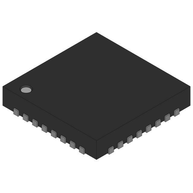


 工商网监
湘ICP备2023018690号
工商网监
湘ICP备2023018690号
