LTM4619
Dual, 26VIN, 4A DC/DC
µModule Regulator
Features
Description
Complete Standalone Power Supply
n Wide Input Voltage Range: 4.5V to 26.5V
(EXTVCC Available for VIN ≤ 5.5V)
n Dual 180° Out-of-Phase Outputs with 4A DC
Typical, 5A Peak Output Current for Each
n Dual Outputs with 0.8V to 5V Range
n Output Voltage Tracking
n ±1.5% Maximum Total DC Output Error
n Current Mode Control/Fast Transient Response
n Power Good
n Phase-Lockable Fixed Frequency 250kHz to 780kHz
n On Board Frequency Synchronization
n Parallel Current Sharing
n Selectable Burst Mode® Operation
n Output Overvoltage Protection
n 15mm × 15mm × 2.82mm LGA Package
The LTM®4619 is a complete dual 4A or single 8A stepdown DC/DC µModule® (micromodule) regulator. Included
in the package are the switching controller, power FETs,
inductor, and all support components. Operating over
input voltage ranges of 4.5V to 26.5V, the LTM4619 supports two outputs with voltage ranges of 0.8V to 5V, each
set by a single external resistor. Its high efficiency design
delivers 4A continuous current (5A peak) for each output.
n
High switching frequency and a current mode architecture
enable a very fast transient response to line and load
changes without sacrificing stability. The two outputs
are interleaved with 180° phase to minimize the ripple
noise and reduce the I/O capacitors. The device supports
frequency synchronization and output voltage tracking for
supply rail sequencing. Burst Mode operation or pulseskipping mode can be selected for light load operations.
Fault protection features include overvoltage protection,
overcurrent protection and foldback current limit for
short-circuit protection.
Applications
Telecom and Networking Equipment
Servers
n Storage Cards
n ATCA Cards
n Industrial Equipment
n Point of Load Regulation
n
The low profile package (2.82mm) enables utilization of
unused space on the bottom of PC boards for high density
point of load regulation. The power module is offered in
a 15mm × 15mm × 2.82mm LGA package. The LTM4619
is RoHS compliant with Pb-free finish.
n
L, LT, LTC, LTM, Linear Technology, the Linear logo, Burst Mode and µModule are registered
trademarks and LTpowerCAD is a trademark of Linear Technology Corporation. All other
trademarks are the property of their respective owners.
Typical Application
Dual 4A 3.3V/2.5V DC/DC µModule Regulator
Efficiency and Power Loss at 12V input
95
VIN
28k
VFB2
VFB1
22pF
VOUT1
2.5V/4A
MODE/PLLIN INTVCC
FREQ/PLLFLTR
COMP1
LTM4619
VOUT1
100µF
COMP2
TK/SS1
0.1µF
22pF
VOUT2
100µF
TK/SS2
RUN1
RUN2
PGOOD
SGND
85
19.1k
VOUT2
3.3V/4A
0.1µF
EXTVCC
1.5
80
75
1.0
70
POWER LOSS
65
0.5
60
PGND
55
4619 TA01a
POWER LOSS (W)
10µF
×2
EFFICIENCY (%)
5.5V TO 26.5V
2.0
EFFICIENCY
90
2.5VOUT
3.3VOUT
0
0.5
1
1.5 2 2.5 3
LOAD CURRENT (A)
3.5
4
0
4619 TA01b
4619fc
For more information www.linear.com/LTM4619
1
�LTM4619
Absolute Maximum Ratings
Pin Configuration
(Note 1)
VIN.............................................................. –0.3V to 28V
INTVCC, PGOOD, RUN1, RUN2, EXTVCC....... –0.3V to 6V
VFB1, VFB2.................................................. –0.3V to 2.7V
COMP1, COMP2 (Note 4)........................... –0.3V to 2.7V
MODE/PLLIN, TK/SS1, TK/SS2,
FREQ/PLLFLTR...................................... –0.3V to INTVCC
VOUT1, VOUT2................................................... 0.8V to 5V
Internal Operating Temperature Range
(Note 2)................................................... –40°C to 125°C
Maximum Reflow Body Temperature..................... 245°C
Storage Temperature Range................... –55°C to 125°C
TOP VIEW
TK/SS2
M
VFB2
COMP2 COMP1
VFB1
TK/SS1
VIN
L
K
RUN2
EXTVCC
SW2
PGOOD
FREQ/PLLFLTR
J
RUN1
SGND
H
SW1
G
MODE/PLLIN
F
INTVCC
E
D
GND
C
VOUT2
VOUT1
B
A
1
2
3
4
5
6
7
8
9
10
11
12
LGA PACKAGE
144-LEAD (15mm × 15mm × 2.82mm)
TJMAX = 125°C, θJA = 13.4°C/W, θJCbottom = 6°C/W, θJCtop = 16°C/W, θJB ≈ θJCbottom,
θJB + θBA = 13.4° C/W, θJA DERIVED FROM 95mm × 76mm PCB WITH 4 LAYERS WEIGHT = 1.7g
Order Information
PART NUMBER
PAD OR BALL FINISH
PART MARKING*
DEVICE
FINISH CODE
PACKAGE
TYPE
MSL
RATING
TEMPERATURE RANGE
(SEE NOTE 2)
LTM4619EV#PBF
Au (RoHS)
LTM4619V
e4
LGA
3
–40°C to 125°C
LTM4619IV#PBF
Au (RoHS)
LTM4619V
e4
LGA
3
–40°C to 125°C
Consult Marketing for parts specified with wider operating temperature
ranges. *Device temperature grade is indicated by a label on the shipping
container. Pad or ball finish code is per IPC/JEDEC J-STD-609.
• Recommended LGA and BGA PCB Assembly and Manufacturing
Procedures:
www.linear.com/umodule/pcbassembly
• Terminal Finish Part Markings:
www.linear.com/leadfree
• LGA and BGA Package and Tray Drawings:
http://www.linear.com/packaging
Electrical Characteristics
The l denotes the specifications which apply over the full internal
operating temperature range (Note 2), otherwise specifications are at TA = 25°C, VIN = 12V. Per typical application in Figure 19.
Specified as each channel. (Note 3)
SYMBOL
PARAMETER
CONDITIONS
MIN
VIN(DC)
Input DC Voltage
VIN ≤ 5.5V, Connect VIN and INTVCC Together
l
VOUT1, 2(RANGE)
Output Voltage Range
VIN = 5.5V to 26.5V
l
VOUT1, 2(DC)
Output Voltage
CIN = 10µF ×1, COUT = 100µF Ceramic, 100µF POSCAP,
RSET = 28.0kΩ
VIN = 12V, VOUT = 2.5V, IOUT = 0A
VIN = 12V, VOUT = 2.5V, IOUT = 4A
l
2.483
2.470
2.00
1.85
TYP
MAX
UNITS
4.5
26.5
V
0.8
5.0
V
2.52
2.52
2.557
2.570
V
V
2.2
2.0
2.35
2.15
V
V
Input Specifications
VIN(UVLO)
2
Undervoltage Lockout Thresholds VINTVCC Rising
VINTVCC Falling
4619fc
For more information www.linear.com/LTM4619
�LTM4619
Electrical
Characteristics
The
l denotes the specifications which apply over the full internal
operating temperature range (Note 2), otherwise specifications are at TA = 25°C, VIN = 12V. Per typical application in Figure 19.
Specified as each channel. (Note 3)
SYMBOL
PARAMETER
CONDITIONS
MIN
TYP
IINRUSH(VIN)
Input Inrush Current at Start-Up
IOUT = 0A, CIN = 10µF, COUT = 100µF, VOUT = 2.5V
VIN = 12V
0.25
IQ(VIN)
Input Supply Bias Current
VIN = 12V, VOUT1 = 2.5V, Switching Continuous
VIN = 12V, VOUT2 = 2.5V, Switching Continuous
VIN = 26.5V, VOUT1 = 2.5V, Switching Continuous
VIN = 26.5V, VOUT2 = 2.5V, Switching Continuous
Shutdown, RUN = 0, VIN = 20V
30
30
40
40
40
IS(VIN)
Input Supply Current
VIN = 12V, VOUT = 2.5V, IOUT = 4A
VIN = 26.5V, VOUT = 2.5V, IOUT = 4A
INTVCC
Internal VCC Voltage
VIN = 12V, VRUN > 2V, No Load
EXTVCC
EXTVCC Switchover Voltage
EXTVCC Ramping Positive
MAX
A
mA
mA
mA
mA
µA
0.97
0.480
l
4.8
5
4.5
4.7
UNITS
A
A
5.2
V
V
Output Specifications
IOUT1, 2(DC)
Output Continuous Current Range VIN = 12V, VOUT = 2.5V (Note 5)
ΔVOUT1(LINE)
Line Regulation Accuracy
VOUT(NOM)
ΔVOUT2(LINE)
Line Regulation Accuracy
VOUT(NOM)
0
4
A
VOUT = 2.5V, VIN from 6V to 26.5V
IOUT = 0A For Each Output
l
0.15
0.25
0.3
0.5
%
%
VOUT = 2.5V, VIN from 6V to 26.5V
IOUT = 0A For Each Output
l
0.15
0.25
0.3
0.5
%
%
Load Regulation Accuracy
For Each Output, VOUT = 2.5V, 0A to 4A (Note 5)
VIN = 12V
l
0.6
0.8
±%
Load Regulation Accuracy
For Each Output, VOUT = 2.5V, 0A to 4A (Note 5)
VIN = 12V
l
0.6
0.8
±%
VOUT1, 2(AC)
Output Ripple Voltage
IOUT = 0A, COUT = 100µF X5R Ceramic
VIN = 12V, VOUT = 2.5V
VIN = 26.5V, VOUT = 2.5V
fS
Output Ripple Voltage Frequency
IOUT = 2A, VIN = 12V, VOUT = 2.5V
FREQ/PLLFLTR = INTVCC
ΔVOUTSTART
Turn-On Overshoot
tSTART
Turn-On Time
ΔVOUT1(LOAD)
VOUT1(NOM)
ΔVOUT2(LOAD)
VOUT2(NOM)
20
25
mV
mV
780
kHz
COUT = 100µF X5R Ceramic, VOUT = 2.5V, IOUT = 0A
VIN = 12V
VIN = 26.5V
10
10
mV
mV
COUT = 100µF X5R Ceramic, VOUT = 2.5V, IOUT = 0A
Resistive Load,
VIN = 12V
VIN = 26.5V
0.250
0.130
ms
ms
ΔVOUTLS
Peak Deviation for Dynamic Load
Load: 0% to 50% to 0% of Full Load
COUT = 100µF X5R Ceramic,VOUT = 2.5V, VIN = 12V
15
mV
tSETTLE
Settling Time for Dynamic Load
Step
Load: 0% to 50% to 0% of Full Load
COUT = 100µF X5R Ceramic,VOUT = 2.5V, VIN = 12V
10
µs
IOUTPK
Output Current Limit
COUT = 100µF X5R Ceramic,
VIN = 6V, VOUT = 2.5V
VIN = 26.5V, VOUT = 2.5V
12
11
A
A
Voltage at VFB Pin
IOUT = 0A, VOUT = 2.5V
Control Section
VFB1, VFB2
l
0.792
0.788
0.8
0.8
0.808
0.810
V
0.9
1.3
1.7
µA
ITK/SS1, 2
Soft-Start Charge Current
VTK/SS = 0V, VOUT = 2.5V
DFMAX
Maximum Duty Factor
In Dropout (Note 4)
97
%
tON(MIN)
Minimum On-Time
(Note 4)
90
ns
4619fc
For more information www.linear.com/LTM4619
3
�LTM4619
electrical
characteristics
The
l denotes the specifications which apply over the full internal
operating temperature range (Note 2), otherwise specifications are at TA = 25°C, VIN = 12V. Per typical application in Figure 19.
Specified as each channel. (Note 3)
SYMBOL
PARAMETER
CONDITIONS
MIN
TYP
MAX
UNITS
fNOM
Nominal Frequency
VFREQ = 1.2V
450
500
550
kHz
fLOW
Lowest Frequency
VFREQ = 0V
210
250
290
kHz
fHIGH
Highest Frequency
VFREQ ≥ 2.4V
700
780
860
kHz
RMODE/PLLIN
MODE/PLLIN Input Resistance
IFREQ
Frequency Setting
Sinking Current
Sourcing Current
VRUN1, 2
RUN Pin ON/OFF Threshold
RFB1, RFB2
Resistor Between VOUT and VFB
Pins for Each Channel
VPGL
PGOOD Voltage Low
IPGOOD = 2mA
IPGOOD
PGOOD Leakage Current
VPGOOD = 5V
ΔVPGOOD
PGOOD Range
VFB Ramping Negative
VFB Ramping Positive
fMODE > fOSC
fMODE < fOSC
RUN Rising
RUN Falling
Note 1: Stresses beyond those listed under Absolute Maximum Ratings
may cause permanent damage to the device. Exposure to any Absolute
Maximum Rating condition for extended periods may affect device
reliability and lifetime.
Note 2: The LTM4619E is guaranteed to meet performance specifications
over the 0°C to 125°C internal operating temperature range. Specifications
over the full –40°C to 125°C internal operating temperature range are
assured by design, characterization and correlation with statistical process
controls. The LTM4619I is guaranteed to meet specifications over the full
95
3.3VOUT
85
EFFICIENCY (%)
90
80
0.8VOUT
75
1.5VOUT
70
60
60
0.5
1
1.5 2 2.5 3
LOAD CURRENT (A)
3.5
4
4619 G01
55
1.35
1.27
V
V
60.1
60.4
60.7
kΩ
0.1
0.3
V
±2
µA
–10
10
%
%
–7.5
7.5
1.2VOUT
5VOUT
3.3VOUT
85
70
65
0
1.5VOUT
75
65
55
4
80
1.22
1.14
Efficiency vs Load Current with
24VIN (f = 500kHz for 1.5VOUT)
90
2.5VOUT
85
1.2VOUT
95
EFFICIENCY (%)
2.5VOUT
90
µA
µA
(Refer to Figures 19 and 20)
5VOUT
3.3VOUT
–13
13
internal operating temperature range. Note that the maximum ambient
temperature consistent with these specifications is determined by specific
operating conditions in conjunction with board layout, the rated package
thermal resistance and other environmental factors.
Note 3: The two outputs are tested separately and the same testing
condition is applied to each output.
Note 4: 100% tested at wafer level only.
Note 5: See Output Current Derating curves for different VIN, VOUT and TA.
Efficiency vs Load Current with
12VIN (f = 500kHz for 1.2VOUT and
1.5VOUT)
EFFICIENCY (%)
95
kΩ
1.1
1.02
–5
5
Typical Performance Characteristics
Efficiency vs Load Current with
5VIN (f = 500kHz for 0.8VOUT,
1.2VOUT and 1.5VOUT)
250
80
75
2.5VOUT
1.5VOUT
70
65
60
55
50
0
0.5
1
1.5 2 2.5 3
LOAD CURRENT (A)
3.5
4
4619 G02
45
0
0.5
1
1.5 2 2.5 3
LOAD CURRENT (A)
3.5
4
4619 G03
4619fc
For more information www.linear.com/LTM4619
�LTM4619
Typical Performance Characteristics
1.2V Output Transient Response
(Refer to Figures 19 and 20)
1.5V Output Transient Response
2.5V Output Transient Response
IOUT
1A/DIV
IOUT
1A/DIV
IOUT
1A/DIV
VOUT
50mV/DIV
VOUT
50mV/DIV
VOUT
50mV/DIV
100µs/DIV
6VIN 1.2VOUT AT 2A/µs LOAD STEP
f = 780kHz
COUT 2× 22µF, 6.3V X5R CERAMIC
COUT 1× 330µF, 6.3V SANYO POSCAP
100µs/DIV
6VIN 1.5VOUT AT 2A/µs LOAD STEP
f = 780kHz
COUT 2× 22µF, 6.3V X5R CERAMIC
COUT 1× 330µF, 6.3V SANYO POSCAP
4619 G04
3.3V Output Transient Response
Start-Up, IOUT = 0A
IOUT
1A/DIV
VOUT
50mV/DIV
100µs/DIV
6VIN 3.3VOUT AT 2A/µs LOAD STEP
f = 780kHz
COUT 2× 22µF, 6.3V X5R CERAMIC
COUT 1× 330µF, 6.3V SANYO POSCAP
100µs/DIV
6VIN 2.5VOUT AT 2A/µs LOAD STEP
f = 780kHz
COUT 2× 22µF, 6.3V X5R CERAMIC
COUT 1× 330µF, 6.3V SANYO POSCAP
4619 G05
Start-Up, IOUT = 4A
VIN
1V/DIV
VIN
1V/DIV
IIN
0.5A/DIV
IIN
0.5A/DIV
20ms/DIV
VIN = 12V, VOUT = 2.5V, IOUT = 0A
COUT = 2× 22µF 10V
AND 1× 100µF 6.3V CERAMIC CAPs
CSOFTSTART = 0.1µF
USE RUN PIN TO CONTROL START-UP
4619 G07
Short Circuit, IOUT = 0A
4619 G06
4619 G08
20ms/DIV
VIN = 12V, VOUT = 2.5V,
IOUT = 4A RESISTIVE LOAD
COUT = 2× 22µF 10V,
AND 1× 100µF 6.3V CERAMIC CAPs
CSOFTSTART = 0.1µF
USE RUN PIN TO CONTROL START-UP
4619 G09
Short Circuit, IOUT = 4A
VOUT
1V/DIV
VOUT
1V/DIV
IIN
0.5A/DIV
IIN
0.5A/DIV
50µs/DIV
VIN = 12V, VOUT = 2.5V, IOUT = 0A
COUT = 2× 22µF 10V,
AND 1× 100µF 6.3V CERAMIC CAPs
4619 G10
50µs/DIV
VIN = 12V, VOUT = 2.5V, IOUT = 4A
COUT = 2× 22µF 10V,
AND 1× 100µF 6.3V CERAMIC CAPs
4619 G11
4619fc
For more information www.linear.com/LTM4619
5
�LTM4619
Pin Functions
PACKAGE ROW AND COLUMN LABELING MAY VARY
AMONG µModule PRODUCTS. REVIEW EACH PACKAGE
LAYOUT CAREFULLY.
VIN (J1 to J3, J10 to J12, K1 to K4, K9 to K12, L1 to L5,
L8 to L12, M1 to M12): Power Input Pins. Apply input
voltage between these pins and PGND pins. Recommend
placing input decoupling capacitance directly between VIN
pins and PGND pins. For VIN < 5.5, tie VIN and INTVCC
together.
VOUT1, VOUT2 (A10 to D10, A11 to D11, A12 to D12, A1 to
D1, A2 to D2, A3 to D3): Power Output Pins. Apply output
load between these pins and PGND pins. Recommend
placing output decoupling capacitance directly between
these pins and PGND pins.
PGND (H1, H2, H4, H9, H11, H12, G1 to G12, F1 to F5,
F7 to F12, E1 to E12, D4 to D9, C4 to C9, B4 to B9, A4 to
A9): Power ground pins for both input and output returns.
INTVCC (F6): Internal 5V Regulator Output. This pin is for
additional decoupling of the 5V internal regulator.
FREQ/PLLFLTR (J8): Frequency Selection Pin. An internal
lowpass filter is tied to this pin. The frequency can be
selected from 250kHz to 780kHz by varying the DC voltage on this pin from 0V to 2.4V. The nominal frequency
setting is 500kHz. Frequency selection can be modified as
long as the inductor ripple current is less ≈40% to 50%
at the output current
1 VOUT
1–
V
VIN OUT
FREQ
IRIPPLE =
L
Where FREQ is selected operating frequency and L is
the inductor value. Leave this pin floating when external
synchronization is used.
TK/SS1, TK/SS2 (K8, K5): Output Voltage Tracking and
Soft-Start Pins. Internal soft-start currents of 1.3µA charge
the soft-start capacitors. See the Applications Information
section to use the tracking function.
EXTVCC (J4): External Power Input to Controller. When
EXTVCC is higher than 4.7V, the internal 5V regulator is
disabled and external power supplies current to reduce
the power dissipation in the module. This will improve the
efficiency more at high input voltages.
VFB1, VFB2 (K7, K6): The negative input of the error
amplifier. Internally, this pin is connected to VOUT with
a 60.4k precision resistor. Different output voltages can
be programmed with an additional resistor between VFB
and SGND pins. See the Applications Information section
for details.
SGND (J6, J7, H6, H7): Signal Ground Pin. Return ground
path for all analog and low power circuitry. Tie a single
connection to PGND in the application.
COMP1, COMP2 (L7, L6): Current Control Threshold and
Error Amplifier Compensation Point. The module has been
internally compensated for most I/O ranges.
MODE/PLLIN (H8): Mode selection or external synchronization pin. Tying this pin high enables pulse-skipping mode.
Tying this pin low enables force continuous operation.
Floating this pin enables Burst Mode operation. A clock
on the pin will force the controller into the continuous
mode of operation and synchronize the internal oscillator.
The suitable synchronizable frequency range is 250kHz to
780kHz subject to inductor ripple current limits described
in the FREQ/PLLFLTR pin section. The external clock input
high threshold is 1.6V, while the input low threshold is 1V.
PGOOD (H5): Output Voltage Power Good Indicator. Open
drain logic output that is pulled to ground when the output
voltage is not within ±7.5% of the regulation point.
RUN1, RUN2 (J9, J5): Run Control Pins. 0.5µA pull-up
currents on these pins turn on the module if these pins
are floating. Forcing either of these pins below 1.2V will
shut down the corresponding outputs. An additional 4.5µA
pull-up current is added to this pin, once the RUN pin rises
above 1.2V. Also, active control or pull-up resistors can
be used to enable the RUN pin. The maximum voltage is
6V on these pins.
SW1, SW2 (H10, H3): Switching Test Pins. These pins
are provided externally to check the operation frequency.
6
4619fc
For more information www.linear.com/LTM4619
�LTM4619
Simplified Block Diagram
INTERNAL
FILTER
+
1.5µF
INTVCC
M1
PGOOD
MODE/PLLIN
EXTVCC
VIN
M2
TK/SS1
R1
R2
R2
R1+ R2 • VIN
= UVLO THRESHOLD = 1.22V
L1
1.5µH
+
10µF
VIN
4.5V TO 26.5V*
CIN
PGND
SW1
VOUT1
2.5V/4A
COUT1
PGND
CSS1
RUN1
60.4k
COMP1
VFB1
INTERNAL
COMP
POWER
CONTROL
TK/SS2
RSET1
28k
1.5µF
M3
PGND
SW2
CSS2
RUN2
COMP2
M4
L2
1.5µH
INTERNAL
COMP
10µF
VOUT2
3.3V/4A
COUT2
PGND
60.4k
FREQ
SGND
+
VFB2
INTERNAL
FILTER
RSET2
19.1k
4619 BD
*USE EXTVCC FOR VIN ≤ 5.5V, OR TIE VIN AND EXTVCC TOGETHER FOR VIN ≤ 5.5V
Figure 1. Simplified LTM4619 Block Diagram
Decoupling Requirements
TA = 25°C. Use Figure 1 configuration.
SYMBOL
PARAMETER
CONDITIONS
CIN
External Input Capacitor Requirement
(VIN = 4.5V to 26.5V, VOUT1 = 2.5V, VOUT2 = 3.3V)
IOUT1 = 4A, IOUT2 = 4A
COUT1
COUT2
External Output Capacitor Requirement
(VIN = 4.5V to 26.5V, VOUT1 = 2.5V, VOUT2 = 3.3V)
IOUT1 = 4A
IOUT2 = 4A
MIN
TYP
10
MAX
UNITS
µF
200
200
µF
µF
4619fc
For more information www.linear.com/LTM4619
7
�LTM4619
Operation
The LTM4619 is a dual-output standalone non-isolated
switching mode DC/DC power supply. It can deliver up to
4A (DC current) for each output with few external input and
output capacitors. This module provides precisely regulated
output voltages programmable via external resistors from
0.8VDC to 5.0VDC over 4.5V to 26.5V input voltages. The
typical application schematic is shown in Figure 19.
The LTM4619 has integrated constant frequency current
mode regulators and built-in power MOSFET devices with
fast switching speed. The typical switching frequency is
780kHz. To reduce switching noise, the two outputs are
interleaved with 180° phase internally and can be synchronized externally using the MODE/PLLIN pin.
With current mode control and internal feedback loop
compensation, the LTM4619 module has sufficient stability margins and good transient performance with a wide
range of output capacitors, even with all ceramic output
capacitors.
Current mode control provides cycle-by-cycle fast current
limit and current foldback in a short-circuit condition.
8
Internal overvoltage and undervoltage comparators pull
the open-drain PGOOD output low if the output feedback
voltage exits a ±7.5% window around the regulation point.
The power good pin is disabled during start-up.
Pulling the RUN pin below 1.2V forces the controller into
its shutdown state, by turning off both MOSFETs. The
TK/SS pin is used for programming the output voltage
ramp and voltage tracking during start-up. See the Applications Information section.
The LTM4619 is internally compensated to be stable over
all operating conditions. LTpowerCAD™ is available for
transient and stability analysis. The VFB pin is used to
program the output voltage with a single external resistor
to ground. Multiphase operation can be easily employed
with the synchronization.
High efficiency at light loads can be accomplished with
selectable Burst Mode operation or pulse-skipping mode
using the MODE/PLLIN pin. Efficiency graphs are provided
for light load operations in the Typical Performance Characteristics section.
4619fc
For more information www.linear.com/LTM4619
�LTM4619
Applications Information
The typical LTM4619 application circuit is shown in
Figure 19. External component selection is primarily determined by the maximum load current and output voltage.
Output Voltage Programming
The PWM controller has an internal 0.8V reference voltage.
As shown in the block diagram, a 60.4k internal feedback
resistor RFB connects VOUT to VFB pin. The output voltage
will default to 0.8V with no feedback resistor. Adding a
resistor RSET from VFB pin to SGND programs the output
voltage:
VOUT = 0.8V •
60.4k +RSET
RSET
or equivalently
RSET =
60.4k
VOUT
– 1
0.8V
VOUT (V)
0.8
1.2
1.5
1.8
2.5
3.3
5
RSET (kΩ)
Open
121
68.1
48.7
28.0
19.1
11.5
Input Capacitors
The LTM4619 module should be connected to a low ACimpedance DC source. Two 1.5µF input ceramic capacitors
are included inside the module. Additional input capacitors
are needed if a large load is required up to the 4A level.
A 47µF to 100µF surface mount aluminum electrolytic
capacitor can be used for more input bulk capacitance.
This bulk capacitor is only needed if the input source impedance is compromised by long inductive leads, traces
or not enough source capacitance.
For a buck converter, the switching duty-cycle can be
estimated as:
ICIN(RMS) =
IOUT(MAX)
η
• D•(1−D)
In the above equation, η is the estimated efficiency of the
power module. The bulk capacitor can be a switcher-rated
aluminum electrolytic capacitor or a polymer capacitor. One
10µF ceramic input capacitor is typically rated for 2A of
RMS ripple current, so the RMS input current at the worst
case for each output at 4A maximum current is about 2A.
If a low inductance plane is used to power the device, then
two 10µF ceramic capacitors are enough for both outputs
at 4A load and no external input bulk capacitor is required.
Output Capacitors
Table 1. RSET Resistor Table vs Various Output Voltages
D=
Without considering the inductor ripple current, for each
output, the RMS current of the input capacitor can be
estimated as:
The LTM4619 is designed for low output voltage ripple
noise. The bulk output capacitors defined as COUT are
chosen with low enough effective series resistance (ESR)
to meet the output voltage ripple and transient requirements. COUT can be a low ESR tantalum capacitor, a low
ESR polymer capacitor or ceramic capacitor. The typical
output capacitance range for each output is from 47µF
to 220µF. Additional output filtering may be required by
the system designer. If further reduction of output ripple
or dynamic transient spikes is required, LTpowerCAD is
available for stability analysis. Multiphase operation will
reduce effective output ripple as a function of the number of phases. Application Note 77 discusses this noise
reduction versus output ripple current cancellation, but
the output capacitance should be considered carefully as
a function of stability and transient response. LTpowerCAD
calculates the output ripple reduction as the number of
implemented phases increased by N times.
VOUT
VIN
4619fc
For more information www.linear.com/LTM4619
9
�LTM4619
applications information
Mode Selections and Phase-Locked Loop
Frequency Selection
The LTM4619 can be enabled to enter high efficiency
Burst Mode operation, constant-frequency pulse-skipping
mode, or forced continuous conduction mode. To select
the forced continuous operation, tie the MODE/PLLIN pin
to a DC voltage below 0.8V. To select pulse-skipping mode
of operation, tie the MODE/PLLIN pin to INTVCC. To select
Burst Mode operation, float the MODE/PLLIN pin.
The switching frequency of the LTM4619’s controllers
can be selected using the FREQ/PLLFLTR pin. If the
MODE/PLLIN pin is not being driven by an external clock
source, the FREQ/PLLFLTR pin can be set from 0V to 2.4V to
program the controller’s operating frequency from 250kHz
to 780kHz using a voltage divider to INTVCC (see Figure
20). The typical frequency is 780kHz. If the output is too
low or the minimum on-time is reached, the frequency
needs to decrease to enlarge the turn-on time. Otherwise,
a significant amount of cycle skipping can occur with correspondingly larger current and voltage ripple.
A phase-lock loop is available on the LTM4619 to synchronize the internal clock to an external clock source
connected on the MODE/PLLIN pin. The clock high level
needs to be higher than 1.6V and the clock low level needs
to be lower than 1V. The frequency programming voltage
and or the programming voltage divider must be removed
from the FREQ/PLLFLTR pin when synchronizing to an
external clock. The FREQ/PLLFLTR pin has the required
onboard PLL filter components for clock synchronization.
The LTM4619 will default to forced continuous mode while
being clock synchronized. Channel 1 is synchronized to
the rising edge on the external clock, and channel 2 is 180
degrees out-of-phase with the external clock.
900
800
SWITCHING FREQUENCY (kHz)
Frequency Synchronization
700
600
500
400
300
200
100
0
0
0.5
1
1.5
2
FREQ/PLLFLTR PIN VOLTAGE (V)
2.5
4619 F02
Figure 2. Switching Frequency vs FREQ/PLLFLTR Pin Voltage
10
4619fc
For more information www.linear.com/LTM4619
�LTM4619
Applications Information
Soft-Start and Tracking
The LTM4619 has the ability to either soft-start by itself
with a capacitor or track the output of another channel or
external supply. When one particular channel is configured
to soft-start by itself, a capacitor should be connected to
its TK/SS pin. This channel is in the shutdown state if its
RUN pin voltage is below 1.2V. Its TK/SS pin is actively
pulled to ground in this shutdown state.
Once the RUN pin voltage is above 1.2V, the channel powers up. A soft-start current of 1.3µA then starts to charge
its soft-start capacitor. Note that soft-start or tracking is
achieved not by limiting the maximum output current of
the controller but by controlling the output ramp voltage
according to the ramp rate on the TK/SS pin. Current
foldback is disabled during this phase to ensure smooth
soft-start or tracking. The soft-start or tracking range is
defined to be the voltage range from 0V to 0.8V on the
TK/SS pin. The total soft-start time can be calculated as:
0.8V •CSS
tSOFT-START =
1.3µA
VIN
5.5V TO
28V
Output voltage tracking can be programmed externally
using the TK/SS pin. The master channel is divided down
with an external resistor divider that is the same as the
slave channel’s feedback divider to implement coincident
tracking. The LTM4619 uses an accurate 60.4k resistor
internally for the top feedback resistor. Figure 3 shows an
example of coincident tracking. Figure 4 shows the output
voltages with coincident tracking.
R1
VSLAVE = 1+ • VTRACK
R2
VTRACK is the track ramp applied to the slave’s TK/SS2
pin. VTRACK has a control range of 0V to 0.8V. When the
master’s output is divided down with the same resistor
values used to set the slave’s output, then the slave will
coincident track with the master until it reaches its final
value. The master will continue to its final value from the
slave’s regulation point.
Ratiometric modes of tracking can be achieved by selecting different divider resistors values to change the output
tracking ratio. The master output must be greater than the
slave output for the tracking to work. Master and slave
data inputs can be used to implement the correct resistors
values for coincident or ratiometric tracking.
MODE/PLLIN INTVCC
VIN
FREQ/PLLFLTR
CIN
R3
19.1k
C2
22pF
VOUT1
3.3V
VFB1
VFB2
COMP1
VOUT1
COUT1
C1
0.1µF
COMP2
LTM4619 V
OUT2
TK/SS1
RUN1
PGOOD
SGND
R4
28k
C3
22pF
VOUT2
2.5V
COUT2
TK/SS2
RUN2
EXTVCC
PGND
4619 F03
MASTER OUTPUT
SLAVE OUTPUT
OUTPUT
VOLTAGE
VOUT1
R1
60.4k
R2
28k
Figure 3. Example of Coincident Tracking
TIME
4619 F04
Figure 4. Coincident Tracking
4619fc
For more information www.linear.com/LTM4619
11
�LTM4619
applications information
0.60
1-PHASE
2-PHASE
3-PHASE
4-PHASE
6-PHASE
0.55
0.50
RMS INPUT RIPPLE CURRENT
DC LOAD CURRENT
0.45
0.40
0.35
0.30
0.25
0.20
0.15
0.10
0.05
0
0.1 0.15
0.2 0.25 0.3 0.35 0.4 0.45 0.5 0.55 0.6 0.65 0.7 0.75 0.8 0.85 0.9
DUTY CYCLE (VOUT/VIN)
4619 F05
Figure 5. Normalized Input RMS Ripple Current vs Duty Cycle for One to Six Phases
1.00
1-PHASE
2-PHASE
3-PHASE
4-PHASE
6-PHASE
0.95
0.90
0.85
0.80
RATIO =
PEAK-TO-PEAK OUTPUT RIPPLE CURRENT
DIr
0.75
0.70
0.65
0.60
0.55
0.50
0.45
0.40
0.35
0.30
0.25
0.20
0.15
0.10
0.05
0
0.1 0.15
0.2 0.25 0.3 0.35 0.4 0.45 0.5 0.55 0.6 0.65 0.7 0.75 0.8 0.85 0.9
DUTY CYCLE (VOUT/VIN)
4619 F06
Figure 6. Normalized Output Ripple Current vs Duty Cycle, Dlr = VOUT T/L
12
4619fc
For more information www.linear.com/LTM4619
�LTM4619
Applications Information
Multiphase Operation
RUN Pin
Multiphase operation with multiple LTM4619 devices in
parallel will lower the effective input RMS ripple current
as well as the output ripple current due to the interleaving
operation of the regulators. Figure 5 provides a ratio of
input RMS ripple current to DC load current as a function
of duty cycle and the number of paralleled phases. Choose
the corresponding duty cycle and the number of phases
to get the correct ripple current value. For example, the
2-phase parallel for one LTM4619 design provides 8A
at 2.5V output from a 12V input. The duty cycle is DC =
2.5V/12V = 0.21. The 2-phase curve has a ratio of ~0.25
for a duty cycle of 0.21. This 0.25 ratio of RMS ripple current to a DC load current of 8A equals ~2A of input RMS
ripple current for the external input capacitors.
The RUN pins can be used to enable or sequence the
particular regulator channel. The RUN pins have their own
internal 0.5µA current source to pull up the pin to 1.2V, and
then the current increases to 4.5µA above 1.2V. Careful
consideration is needed to assure that board contamination
or residue does not load down the 0.5µA pull-up current.
Otherwise active control to these pins can be used to enable the regulators. A voltage divider can be used from
VIN to set an enable point that can also be used as a UVLO
feature for the regulator. The resistor divider needs to be
low enough resistance to swamp out the pull-up current
sources to prevent unintended activation of the device.
See the Simplified Block Diagram.
The effective output ripple current is lowered with multiphase operations as well. Figure 6 provides a ratio of
peak-to-peak output ripple current to the normalized
output ripple current as a function of duty cycle and the
number of paralleled phases. Choose the corresponding
duty cycle and the number of phases to get the correct
output ripple current ratio value. If a 2-phase operation
is chosen at 12VIN to 2.5VOUT with a duty cycle of 21%,
then 0.6 is the ratio of the normalized output ripple current to inductor ripple DIr at zero duty cycle. This leads
to ~1.3A of the effective output ripple current ΔIL if the
DIr is at 2.2A. Refer to Application Note 77 for a detailed
explanation of the output ripple current reduction as a
function of paralleled phases.
Power Good
The PGOOD pin is connected to the open drain of an internal
N-channel MOSFET. The MOSFET turns on and pulls the
PGOOD pin low when either VFB pin voltage is not within
±7.5% of the 0.8V reference voltage. The PGOOD pin is
also pulled low when either RUN pin is below 1.2V or when
the LTM4619 is in the soft-start or tracking phase. When
the VFB pin voltage is within the ±7.5% requirement, the
MOSFET is turned off and the pin is allowed to be pulled
up by an external resistor to a source of up to 6V. The
PGOOD pin will flag power good immediately when both
VFB pins are within the ±7.5% window. However, there is
an internal 17µs power bad mask when either VFB goes
out of the ±7.5% window.
The output ripple voltage has two components that are
related to the amount of bulk capacitance and effective
series resistance (ESR) of the output bulk capacitance.
Therefore, the output ripple voltage can be calculated with
the known effective output ripple current. The equation:
ΔVOUT(P-P) ≈ ΔIL/(8 • f • N • COUT) + ESR • ΔIL
where f is frequency and N is the number of parallel phases.
4619fc
For more information www.linear.com/LTM4619
13
�LTM4619
applications information
INTVCC and EXTVCC
The INTVCC is the internal 5V regulator that powers the
LTM4619 internal circuitry and drives the power MOSFETs.
The input voltage of the LTM4619 must be 6V or above
for the INTVCC to regulate to the proper 5V level due to
the internal LDO dropout from the input voltage. For applications that need to operate below 6V input, then the
input voltage can be connected directly to the EXTVCC
pin to bypass the LDO dropout concern, or an external
5V supply can be used to power the EXTVCC pin when
the input voltage is at high end of the supply range to
reduce power dissipation in the module. For example the
dropout voltage for 24V input would be 24V – 5V = 19V.
This 19V headroom then multiplied by the power MOSFET
drive current of ~15mA would equal ~0.3W additional
power dissipation. So utilizing an external 5V supply on
the EXTVCC would improve design efficiency and reduce
device temperature rise.
Slope Compensation
The module has already been internally compensated for
all output voltages. LTpowerCAD is available for control
loop optimization.
Burst Mode Operation and Pulse-Skipping Mode
The LTM4619 regulator can be placed into high efficiency
power saving modes at light load condition to conserve
power. The Burst Mode operation can be selected by floating the MODE/PLLIN pin, and pulse-skipping mode can be
selected by pulling the MODE/PLLIN pin to INTVCC. Burst
Mode operation offers the best efficiency at light load, but
output ripple will be higher and lower frequency ranges
are capable which can interfere with some systems. Pulseskipping mode efficiency is not as good as Burst Mode
operation, but this mode only skips pulses to save efficiency
and maintains a lower output ripple and a higher switching frequency. Burst Mode operation and pulse-skipping
mode efficiencies can be reviewed in graph supplied in
the Typical Performance Characteristics section.
14
Fault Conditions: Current Limit and Overcurrent
Foldback
The LTM4619 has a current mode controller, which inherently limits the cycle-by-cycle inductor current not only in
steady-state operation, but also in transient.
To further limit current in the event of an overload condition, the LTM4619 provides foldback current limiting. If the
output voltage falls by more than 50%, then the maximum
output current is progressively lowered to one-third of its
full current limit value. Foldback current limiting is disabled
during soft-start and tracking up.
Thermal Considerations and Output Current Derating
The thermal resistances reported in the Pin Configuration
section of the data sheet are consistent with those parameters defined by JESD51-12 and are intended for use with
finite element analysis (FEA) software modeling tools that
leverage the outcome of thermal modeling, simulation,
and correlation to hardware evaluation performed on a
µModule package mounted to a hardware test board.
The motivation for providing these thermal coefficients
is found in JESD51-12 (“Guidelines for Reporting and
Using Electronic Package Thermal Information”).
Many designers may opt to use laboratory equipment
and a test vehicle such as the demo board to predict the
µModule regulator’s thermal performance in their application at various electrical and environmental operating
conditions to compliment any FEA activities. Without FEA
software, the thermal resistances reported in the Pin Configuration section are, in and of themselves, not relevant to
providing guidance of thermal performance; instead, the
derating curves provided in this data sheet can be used
in a manner that yields insight and guidance pertaining to
one’s application-usage, and can be adapted to correlate
thermal performance to one’s own application.
The Pin Configuration section gives four thermal coefficients explicitly defined in JESD51-12; these coefficients
are quoted or paraphrased in the following:
4619fc
For more information www.linear.com/LTM4619
�LTM4619
applications information
1 θJA, the thermal resistance from junction to ambient, is
the natural convection junction-to-ambient air thermal
resistance measured in a one cubic foot sealed enclosure. This environment is sometimes referred to as
“still air” although natural convection causes the air to
move. This value is determined with the part mounted
to a 95mm × 76mm PCB with four layers.
2 θJCbottom, the thermal resistance from junction to the
bottom of the product case, is determined with all of
the component power dissipation flowing through the
bottom of the package. In the typical µModule regulator,
the bulk of the heat flows out the bottom of the package, but there is always heat flow out into the ambient
environment. As a result, this thermal resistance value
may be useful for comparing packages but the test
conditions don’t generally match the user’s application.
3 θJCtop, the thermal resistance from junction to top of
the product case, is determined with nearly all of the
component power dissipation flowing through the top of
the package. As the electrical connections of the typical
µModule regulator are on the bottom of the package, it
is rare for an application to operate such that most of
the heat flows from the junction to the top of the part.
As in the case of θJCbottom, this value may be useful
for comparing packages but the test conditions don’t
generally match the user’s application.
4 θJB, the thermal resistance from junction to the printed
circuit board, is the junction-to-board thermal resistance
where almost all of the heat flows through the bottom
of the µModule package and into the board, and is really
the sum of the θJCbottom and the thermal resistance of
the bottom of the part through the solder joints and a
portion of the board. The board temperature is measured
a specified distance from the package.
A graphical representation of the aforementioned thermal resistances is given in Figure 7; blue resistances are
contained within the µModule regulator, whereas green
resistances are external to the µModule package.
As a practical matter, it should be clear to the reader that
no individual or sub-group of the four thermal resistance
parameters defined by JESD51-12 or provided in the
Pin Configuration section replicates or conveys normal
operating conditions of a µModule regulator. For example,
in normal board-mounted applications, never does 100%
of the device’s total power loss (heat) thermally conduct exclusively through the top or exclusively through
bottom of the µModule package—as the standard defines
for θJCtop and θJCbottom, respectively. In practice, power
loss is thermally dissipated in both directions away from
the package—granted, in the absence of a heat sink and
airflow, a majority of the heat flow is into the board.
Within the LTM4619, be aware there are multiple power
devices and components dissipating power, with a consequence that the thermal resistances relative to different
junctions of components or die are not exactly linear with
respect to total package power loss. To reconcile this
complication without sacrificing modeling simplicity—but
also not ignoring practical realities—an approach has been
taken using FEA software modeling along with laboratory
testing in a controlled-environment chamber to reasonably define and correlate the thermal resistance values
supplied in this data sheet: (1) Initially, FEA software is
used to accurately build the mechanical geometry of the
LTM4619 and the specified PCB with all of the correct
material coefficients along with accurate power loss source
definitions; (2) this model simulates a software-defined
JEDEC environment consistent with JESD51-12 to predict
power loss heat flow and temperature readings at different
interfaces that enable the calculation of the JEDEC-defined
thermal resistance values; (3) the model and FEA software
is used to evaluate the LTM4619 with heat sink and airflow;
(4) having solved for and analyzed these thermal resistance values and simulated various operating conditions
in the software model, a thorough laboratory evaluation
replicates the simulated conditions with thermocouples
within a controlled-environment chamber while operating the device at the same power loss as that which was
simulated. The outcome of this process and due diligence
yields the set of derating curves shown in this data sheet.
4619fc
For more information www.linear.com/LTM4619
15
�LTM4619
applications information
JUNCTION-TO-AMBIENT THERMAL RESISTANCE COMPONENTS
CASE (TOP)-TO-AMBIENT
RESISTANCE
JUNCTION-TO-CASE (TOP)
RESISTANCE
JUNCTION
JUNCTION-TO-BOARD RESISTANCE
AMBIENT
JUNCTION-TO-CASE
CASE (BOTTOM)-TO-BOARD
(BOTTOM) RESISTANCE
RESISTANCE
BOARD-TO-AMBIENT
RESISTANCE
4619 F07
µMODULE DEVICE
Figure 7. Graphical Representation of JESD51-12 Thermal Coefficients
The 1.5V and 3.3V power loss curves in Figures 8 and 9
can be used in coordination with the load current derating
curves in Figures 10 to 17 for calculating an approximate
ΘJA thermal resistance for the LTM4619 with various heat
sinking and airflow conditions. The power loss curves are
taken at room temperature, and are increased with a 1.35
multiplicative factor at 120°C. The derating curves are plotted with CH1 and CH2 in parallel single output operation
starting at 8A of load with low ambient temperature. The
output voltages are 1.5V and 3.3V. These are chosen to
include the lower and higher output voltage ranges for correlating the thermal resistance. Thermal models are derived
from several temperature measurements in a controlled
temperature chamber along with thermal modeling analysis.
The junction temperatures are monitored while ambient
temperature is increased with and without airflow. The
power loss increase with ambient temperature change
is factored into the derating curves. The junctions are
maintained at ~120°C maximum while lowering output
current or power while increasing ambient temperature.
The decreased output current will decrease the internal
module loss as ambient temperature is increased.
The monitored junction temperature of 120°C minus
the ambient operating temperature specifies how much
module temperature rise can be allowed. As an example in
Figure 12, the load current is derated to 5A at ~95°C with
no air or heat sink and the power loss for the 12V to 1.5V
at 5A output is about 1.83W. The 1.83W loss is calculated
with the 1.35W room temperature loss from the 12V to
16
1.5V power loss curve at 5A, and the 1.35 multiplying
factor at 120°C ambient. If the 95°C ambient temperature
is subtracted from the 120°C junction temperature, then
the difference of 25°C divided by 1.83W equals a 13.6°C/W
ΘJA thermal resistance. Table 2 specifies a 13.4°C/W value
which is pretty close. The airflow graphs are more accurate
due to the fact that the ambient temperature environment is
controlled better with airflow. As an example in Figure 14,
the load current is derated to 5A at ~95°C with 400LFM of
airflow and the power loss for the 12V to 3.3V at 5A output
is ~2.5W. The 2.5W loss is calculated with the ~1.85W room
temperature loss from the 12V to 3.3V power loss curve at
5A, and the 1.35 multiplying factor at 120°C ambient. If the
95°C ambient temperature is subtracted from the 120°C
junction temperature, then the difference of 25°C divided
by 2.5W equals a 10°C/W θJA thermal resistance. Table 2
specifies a 9.7°C/W value which is pretty close. Tables 2
and 3 provide equivalent thermal resistances for 1.5V and
3.3V outputs with and without airflow and heat sinking.
The derived thermal resistances in Tables 2 and 3 for the
various conditions can be multiplied by the calculated
power loss as a function of ambient temperature to derive
temperature rise above ambient, thus maximum junction
temperature. Room temperature power loss can be derived
from the efficiency curves and adjusted with the above
ambient temperature multiplicative factors. The printed
circuit board is a 1.6mm thick four layer board with two
ounce copper for the two outer layers and one ounce
copper for the two inner layers. The PCB dimensions are
95mm × 76mm. The BGA heat sinks are listed in Table 3.
4619fc
For more information www.linear.com/LTM4619
�LTM4619
applications information
Table 2. 1.5V Output
DERATING CURVE
VIN (V)
POWER LOSS CURVE
AIRFLOW (LFM)
HEATSINK
ΘJA (°C/W)
Figures 10, 12
6, 12
Figure 8
0
none
13.4
Figures 10, 12
6, 12
Figure 8
200
none
11.2
Figures 10, 12
6, 12
Figure 8
400
none
9.7
Figures 11, 13
6, 12
Figure 8
0
BGA Heatsink
12.6
Figures 11, 13
6, 12
Figure 8
200
BGA Heatsink
10.0
Figures 11, 13
6, 12
Figure 8
400
BGA Heatsink
9.6
Table 3. 3.3V Output
DERATING CURVE
VIN (V)
POWER LOSS CURVE
AIRFLOW (LFM)
HEATSINK
ΘJA (°C/W)
Figures 14, 16
12, 24
Figure 9
0
none
13.4
Figures 14, 16
12, 24
Figure 9
200
none
11.2
Figures 14, 16
12, 24
Figure 9
400
none
9.7
Figures 15, 17
12, 24
Figure 9
0
BGA Heatsink
12.6
Figures 15, 17
12, 24
Figure 9
200
BGA Heatsink
10.0
Figures 15, 17
12, 24
Figure 9
400
BGA Heatsink
9.6
HEATSINK MANUFACTURER
PART NUMBER
WEBSITE
Aavid Thermalloy
375424B00034G
www.aavidthermalloy.com
Cool Innovations
4-050503P to 4-050508P
www.coolinnovations.com
4.5
3.0
4.0
3.5
POWER LOSS (W)
POWER LOSS (W)
2.5
2.0
1.5
1.0
2.5
2.0
1.5
1.0
0.5
0
3.0
0.5
6V LOSS
12V LOSS
0
2
4
6
LOAD CURRENT (A)
8
0
0
2
4
6
LOAD CURRENT (A)
8
4619 F09
4619 F08
Figure 8. Power Loss at 1.5V Output
12V LOSS
24V LOSS
Figure 9. Power Loss at 3.3V Output
4619fc
For more information www.linear.com/LTM4619
17
�LTM4619
8
8
7
7
6
6
LOAD CURRENT (A)
LOAD CURRENT (A)
applications information
5
4
3
2
4
3
2
6VIN TO 1.5VOUT 0LFM
6VIN TO 1.5VOUT 200LFM
6VIN TO 1.5VOUT 400LFM
1
0
5
70
75
6VIN TO 1.5VOUT 0LFM
6VIN TO 1.5VOUT 200LFM
6VIN TO 1.5VOUT 400LFM
1
80 85 90 95 100 105 110 115
AMBIENT TEMPERATURE (°C)
0
70
75
80 85 90 95 100 105 110 115
AMBIENT TEMPERATURE (°C)
4619 F10
Figure 11. 6VIN to 1.5VOUT
with Heat Sink
Figure 10. 6VIN to
1.5VOUT without Heat Sink
8
8
7
7
7
6
6
6
5
4
3
2
5
4
3
70
75
12VIN TO 1.5VOUT 0LFM
12VIN TO 1.5VOUT 200LFM
12VIN TO 1.5VOUT 400LFM
1
0
80 85 90 95 100 105 110 115
AMBIENT TEMPERATURE (°C)
70
75
4
3
0
4619 F14
4619 F13
Figure 14. 12VIN to 3.3VOUT
without Heat Sink
7
7
7
6
6
6
3
2
5
4
3
2
12VIN TO 3.3VOUT 0LFM
12VIN TO 3.3VOUT 200LFM
12VIN TO 3.3VOUT 400LFM
1
0
LOAD CURRENT (A)
8
LOAD CURRENT (A)
8
4
4619 F15
Figure 15. 12VIN to 3.3VOUT
with Heat Sink
18
0
5
4
3
2
24VIN TO 3.3VOUT 0LFM
24VIN TO 3.3VOUT 200LFM
24VIN TO 3.3VOUT 400LFM
1
60 65 70 75 80 85 90 95 100 105 110
AMBIENT TEMPERATURE (°C)
60 65 70 75 80 85 90 95 100 105 110
AMBIENT TEMPERATURE (°C)
Figure 13. 12VIN to 1.5VOUT
with Heat Sink
8
5
12VIN TO 3.3VOUT 0LFM
12VIN TO 3.3VOUT 200LFM
12VIN TO 3.3VOUT 400LFM
1
80 85 90 95 100 105 110 115
AMBIENT TEMPERATURE (°C)
4619 F12
Figure 12. 12VIN to 1.5VOUT
without Heat Sink
LOAD CURRENT (A)
5
2
2
12VIN TO 1.5VOUT 0LFM
12VIN TO 1.5VOUT 200LFM
12VIN TO 1.5VOUT 400LFM
1
0
LOAD CURRENT (A)
8
LOAD CURRENT (A)
LOAD CURRENT (A)
4619 F11
40
50
60
70
80
90
AMBIENT TEMPERATURE (°C)
24VIN TO 3.3VOUT 0LFM
24VIN TO 3.3VOUT 200LFM
24VIN TO 3.3VOUT 400LFM
1
100
4619 F16
Figure 16. 24VIN to 3.3VOUT
without Heat Sink
0
40
50
60
70
80
90
AMBIENT TEMPERATURE (°C)
100
4619 F17
Figure 17. 24VIN to 3.3VOUT
with Heat Sink
4619fc
For more information www.linear.com/LTM4619
�LTM4619
Applications information
Safety Considerations
• Place high frequency ceramic input and output capacitors next to the VIN, PGND and VOUT pins to minimize
high frequency noise.
The LTM4619 modules do not provide galvanic isolation
from VIN to VOUT. There is no internal fuse. If required,
a slow blow fuse with a rating twice the maximum input
current needs to be provided to protect each unit from
catastrophic failure.
• Place a dedicated power ground layer underneath the
unit.
• To minimize the via conduction loss and reduce module
thermal stress, use multiple vias for interconnections
between top layer and other power layers.
Layout Checklist/Example
The high integration of LTM4619 makes the PCB board
layout very simple and easy. However, to optimize its electrical and thermal performance, some layout considerations
are still necessary.
• Do not put vias directly on the pads.
• Use a separated SGND ground copper area for components connected to signal pins. Connect the SGND
to PGND underneath the unit.
• Use large PCB copper areas for high current path, including VIN, PGND, VOUT1 and VOUT2. It helps to minimize
the PCB conduction loss and thermal stress.
• Decouple the input and output grounds to lower the
output ripple noise.
Figure 18 gives a good example of the recommended layout.
TOP VIEW
PGND
VIN
PGND
M
CIN2
L
CIN1
K
J
H
G
F
E
D
C
B
A
1
2
3
4
5
6
7
8
9
10
11
COUT2
VOUT2
12
COUT1
PGND
VOUT1
Figure 18. Recommended PCB Layout
4619fc
For more information www.linear.com/LTM4619
19
�LTM4619
Typical Applications
VIN
4.5V TO 26.5V
VOUT1
5V/4A
CIN
10µF
×2
VIN
11.5k
C1
22pF
VFB1
100k
PGOOD
C2
22pF
COMP2
LTM4619
TK/SS1
0.1µF
19.1k
VFB2
COMP1
VOUT1
COUT1
100µF
INTVCC
MODE/PLLIN INTVCC
FREQ/PLLFLTR
COUT2
100µF
TK/SS2
RUN1
PGOOD
SGND
VOUT2
0.1µF
RUN2
PGND
EXTVCC
VOUT2
3.3V/4A
R1 (OPT*)
VIN
4619 F19
*STUFF WITH A 0Ω RESISTOR FOR 4.5V < VIN < 5.5V
Figure 19. Typical 4.5V to 26.5V Input, 5V and 3.3V Outputs at 4A Design
20
4619fc
For more information www.linear.com/LTM4619
�LTM4619
TYPICAL applications
EXTERNAL 5V SUPPLY FOR
INPUT VOLTAGE BELOW 5.5V
VIN
4.5V TO
26.5V
VOUT1
1.2V/4A
MODE/PLLIN
CIN
10µF
×2
VIN
121k
C1
22pF
VFB1
VFB2
COMP1
VOUT1
COUT1
100µF
×2
INTVCC EXTVCC
FREQ/PLLFLTR
COMP2
LTM4619
TK/SS1
0.1µF
INTVCC
PGOOD
SGND
C2
22pF
VOUT2
RUN2
R2
1.21k
68.1k
TK/SS2
RUN1
100k
R1
3.83k
0.1µF
COUT2
100µF
×2
VOUT2
1.5V/4A
PGND
4619 F20
PGOOD
Figure 20. Typical 4.5V to 26.5V Input, 1.2V and 1.5V
Outputs at 4A Design with Adjusted Frequency at 500kHz
VIN
6V TO
26.5V
CIN
10µF
MODE/PLLIN EXTVCC INTVCC
VIN
FREQ/PLLFLTR
COMP1
VFB1
COMP2
VFB2
TK/SS1
C3
0.1µF
LTM4619
C1
51pF
VOUT1
TK/SS2
VOUT2
PGOOD
RUN2
C4
100µF
R1
5.76k
+
VOUT2
5V/8A
C5
330µF
RUN1
SGND
PGND
4619 F21
Figure 21. Output Paralleled LTM4619 Module for 5V Output at 8A Design
4619fc
For more information www.linear.com/LTM4619
21
�LTM4619
TYPICAL applications
CLOCK SYNC, 0° PHASE
VIN
6V TO 26.5V
+
CIN2
10µF
2x
CIN1
330µF
VOUT1
5V/4A
VIN
+
R3
11.5k
C10
22pF
VFB2
VFB1
COMP1
C1
0.1µF
COMP2
LTM4619
VOUT1
C3
22µF
C2
220µF
MODE/PLLIN INTVCC
FREQ/PLLFLTR
TK/SS1
TK/SS2
RUN1
2 PHASE OSCILLATOR
R9
143k
C3
0.1µF
R7
28k
+
C9
220µF
VOUT2
3.3V/4A
C5
220µF
+
VOUT4
1.8V/4A
C7
220µF
R2
19.1k
PGND
CLOCK SYNC, 90° PHASE
MOD
VIN
VOUT3
2.5V/4A
C4
22µF
+
ON/OFF
GND LTC6908-2 OUT2
SET
R1
60.4k
R4
19.1k
EXTVCC
SGND
OUT1
VOUT1
RUN2
PGOOD
V+
VOUT2
C11
22pF
C8
22µF
C12
22pF
VOUT1
R10
60.4k
MODE/PLLIN INTVCC
FREQ/PLLFLTR
VFB1
VFB2
COMP1
COMP2
LTM4619
VOUT1
TK/SS1
TK/SS2
RUN1
VOUT1
RUN2
PGOOD
R11
28k
VOUT2
C13
22pF
SGND
R5
60.4k
R8
48.7k
C6
22µF
EXTVCC
PGND
4619 F22
R6
48.7k
Figure 22. 4-Phase, Four Outputs (5V, 3.3V, 2.5V and 1.8V) with Tracking
22
4619fc
For more information www.linear.com/LTM4619
�LTM4619
Package Description
PACKAGE ROW AND COLUMN LABELING MAY VARY
AMONG µModule PRODUCTS. REVIEW EACH PACKAGE
LAYOUT CAREFULLY.
Pin Assignment Table 4
(Arranged by Pin Function)
PIN NAME
PIN NAME
PIN NAME
PIN NAME
A1
A2
A3
A4
A5
A6
A7
A8
A9
A10
A11
A12
VOUT2
VOUT2
VOUT2
PGND
PGND
PGND
PGND
PGND
PGND
VOUT1
VOUT1
VOUT1
D1
D2
D3
D4
D5
D6
D7
D8
D9
D10
D11
D12
VOUT2
VOUT2
VOUT2
PGND
PGND
PGND
PGND
PGND
PGND
VOUT1
VOUT1
VOUT1
G1
G2
G3
G4
G5
G6
G7
G8
G9
G10
G11
G12
PGND
PGND
PGND
PGND
PGND
PGND
PGND
PGND
PGND
PGND
PGND
PGND
K1
K2
K3
K4
K5
K6
K7
K8
K9
K10
K11
K12
VIN
VIN
VIN
VIN
TK/SS2
VFB2
VFB1
TK/SS1
VIN
VIN
VIN
VIN
B1
B2
B3
B4
B5
B6
B7
B8
B9
B10
B11
B12
VOUT2
VOUT2
VOUT2
PGND
PGND
PGND
PGND
PGND
PGND
VOUT1
VOUT1
VOUT1
E1
E2
E3
E4
E5
E6
E7
E8
E9
E10
E11
E12
PGND
PGND
PGND
PGND
PGND
PGND
PGND
PGND
PGND
PGND
PGND
PGND
H1
H2
H3
H4
H5
H6
H7
H8
H9
H10
H11
H12
PGND
PGND
SW2
PGND
PGOOD
SGND
SGND
MODE/PLLIN
PGND
SW1
PGND
PGND
L1
L2
L3
L4
L5
L6
L7
L8
L9
L10
L11
L12
VIN
VIN
VIN
VIN
VIN
COMP2
COMP1
VIN
VIN
VIN
VIN
VIN
C1
C2
C3
C4
C5
C6
C7
C8
C9
C10
C11
C12
VOUT2
VOUT2
VOUT2
PGND
PGND
PGND
PGND
PGND
PGND
VOUT1
VOUT1
VOUT1
F1
F2
F3
F4
F5
F6
F7
F8
F9
F10
F11
F12
PGND
PGND
PGND
PGND
PGND
INTVCC
PGND
PGND
PGND
PGND
PGND
PGND
J1
J2
J3
J4
J5
J6
J7
J8
J9
J10
J11
J12
VIN
VIN
VIN
EXTVCC
RUN2
SGND
SGND
FREQ/PLLFLTR
RUN1
VIN
VIN
VIN
M1
M2
M3
M4
M5
M6
M7
M8
M9
M10
M11
M12
VIN
VIN
VIN
VIN
VIN
VIN
VIN
VIN
VIN
VIN
VIN
VIN
4619fc
For more information www.linear.com/LTM4619
23
�4
For more information www.linear.com/LTM4619
3.1750
3.1750
SUGGESTED PCB LAYOUT
TOP VIEW
1.9050
PACKAGE TOP VIEW
E
0.6350
0.0000
0.6350
PIN “A1”
CORNER
1.9050
Y
6.9850
5.7150
4.4450
3.1750
1.9050
0.6350
0.0000
0.6350
1.9050
3.1750
4.4450
5.7150
6.9850
X
D
aaa Z
0.27
2.45
MIN
2.72
0.60
NOM
2.82
0.63
15.00
15.00
1.27
13.97
13.97
0.32
2.50
DIMENSIONS
eee S X Y
H1
SUBSTRATE
0.37
2.55
0.15
0.10
0.05
MAX
2.92
0.66
NOTES
DETAIL B
PACKAGE SIDE VIEW
TOTAL NUMBER OF LGA PADS: 144
SYMBOL
A
b
D
E
e
F
G
H1
H2
aaa
bbb
eee
DETAIL A
0.630 ±0.025 SQ. 143x
DETAIL B
H2
MOLD
CAP
A
(Reference LTC DWG # 05-08-1816 Rev C)
bbb Z
24
Z
LGA Package
144-Lead (15mm × 15mm × 2.82mm)
e
b
11
10
9
7
G
6
e
5
PACKAGE BOTTOM VIEW
8
4
3
2
1
DETAIL A
DETAILS OF PIN #1 IDENTIFIER ARE OPTIONAL,
BUT MUST BE LOCATED WITHIN THE ZONE INDICATED.
THE PIN #1 IDENTIFIER MAY BE EITHER A MOLD OR
MARKED FEATURE
4
7
TRAY PIN 1
BEVEL
!
PACKAGE IN TRAY LOADING ORIENTATION
LTMXXXXXX
µModule
A
B
C
D
E
F
G
H
J
K
L
M
7
SEE NOTES
DIA 0.630
PAD 1
LGA 144 1112 REV C
PACKAGE ROW AND COLUMN LABELING MAY VARY
AMONG µModule PRODUCTS. REVIEW EACH PACKAGE
LAYOUT CAREFULLY
6. THE TOTAL NUMBER OF PADS: 144
5. PRIMARY DATUM -Z- IS SEATING PLANE
BALL DESIGNATION PER JESD MS-028 AND JEP95
3
2. ALL DIMENSIONS ARE IN MILLIMETERS
NOTES:
1. DIMENSIONING AND TOLERANCING PER ASME Y14.5M-1994
COMPONENT
PIN “A1”
3
SEE NOTES
F
b
12
3x, C (0.22 x45°)
LTM4619
Package Description
4619fc
6.9850
5.7150
4.4450
4.4450
5.7150
6.9850
aaa Z
�LTM4619
Revision History
(Revision history begins at Rev B)
REV
DATE
DESCRIPTION
B
08/13
Added “or single 8A” to Description
C
05/14
PAGE NUMBER
1
Changed MODE to MODE/PLLIN
8
Changed GND to PGND
22
Added Design Resources
24
Update Order Information Table
2
Update thermal resistance figures
Update Thermal Considerations Section
2, 17
14, 15, 16
4619fc
Information furnished by Linear Technology Corporation is believed to be accurate and reliable.
However, no responsibility is assumed for its use. Linear Technology Corporation makes no representation that the interconnection
of its circuits
as described
herein will not infringe on existing patent rights.
For more
information
www.linear.com/LTM4619
25
�LTM4619
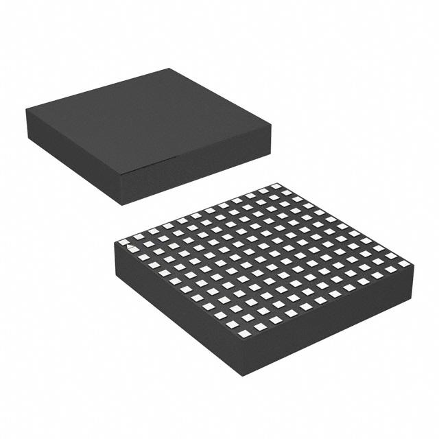
Package Photograph
Related Parts
PART NUMBER DESCRIPTION
COMMENTS
LTM4614
Dual, 4A, Low VIN, DC/DC µModule Regulator
2.375V ≤ VIN ≤ 5.5V, 0.8V ≤ VOUT ≤ 5V, 15mm × 15mm × 2.82mm LGA
LTM4615
Triple, Low VIN, DC/DC µModule Regulator
Two 4A Outputs and One 1.5A, 15mm × 15mm × 2.82mm LGA
LTM4616
Dual, 8A, Low VIN, DC/DC µModule Regulator
2.7V ≤ VIN ≤ 5.5V, 0.6V ≤ VOUT ≤ 5V, 15mm × 15mm × 2.82mm LGA
LTM4628
Dual, 8A, 26V, DC/DC µModule Regulator
4.5V ≤ VIN ≤ 28.5V, 0.6V ≤ VOUT ≤ 5.5V, Remote Sense Amplifier, Internal
Temperature Sensing Diode Output, 15mm × 15mm × 4.32mm LGA
LTM4620A
Dual, 16V, 13A, 26A, Step-Down µModule Regulator
4.5V ≤ VIN ≤ 16V, 0.6V ≤ VOUT ≤ 5.3V, 15mm × 15mm × 4.41mm LGA
Design Resources
SUBJECT
DESCRIPTION
µModule Design and Manufacturing Resources
Design:
• Selector Guides
• Demo Boards and Gerber Files
• Free Simulation Tools
µModule Regulator Products Search
1. Sort table of products by parameters and download the result as a spread sheet.
Manufacturing:
• Quick Start Guide
• PCB Design, Assembly and Manufacturing Guidelines
• Package and Board Level Reliability
2. Search using the Quick Power Search parametric table.
TechClip Videos
Quick videos detailing how to bench test electrical and thermal performance of µModule products.
Digital Power System Management
Linear Technology’s family of digital power supply management ICs are highly integrated solutions that
offer essential functions, including power supply monitoring, supervision, margining and sequencing,
and feature EEPROM for storing user configurations and fault logging.
26 Linear Technology Corporation
1630 McCarthy Blvd., Milpitas, CA 95035-7417
For more information www.linear.com/LTM4619
(408) 432-1900 ● FAX: (408) 434-0507
●
www.linear.com/LTM4619
4619fc
LT 0514 REV C • PRINTED IN USA
LINEAR TECHNOLOGY CORPORATION 2009
�


 工商网监
湘ICP备2023018690号
工商网监
湘ICP备2023018690号
