MAX15002
Dual-Output Buck Controller with
Tracking/Sequencing
General Description
The MAX15002 is a dual-output, pulse-width-modulated
(PWM), step-down DC-DC controller with tracking and
sequencing options. The device operates over the input
voltage range of 5.5V to 23V or 5V ±10%. Each PWM
controller provides an adjustable output down to 0.6V and
delivers at least 15A of load current with excellent load
and line regulation. The MAX15002 is optimized for highperformance, small-size power management solutions.
The options of Coincident Tracking, Ratiometric
Tracking, and Output Sequencing allow the tailoring of
the power-up/power-down sequence depending on the
system requirements. Each of the MAX15002 PWM sections utilizes a voltage-mode control scheme with external compensation, allowing for good noise immunity
and maximum flexibility with a wide selection of inductor values and capacitor types. Each PWM section
operates at the same, fixed switching frequency that is
programmable from 200kHz to 2.2MHz and can be synchronized to an external clock signal using the SYNC
input. Each converter operating at up to 2.2MHz with
180° out-of-phase, increases the input capacitor ripple
frequency up to 4.4MHz, thereby significantly reducing
the RMS input ripple current and the size of the input
bypass capacitor requirement.
The MAX15002 includes internal undervoltage lockout
with hysteresis, digital soft-start/soft-stop for glitch-free
power-up and power-down of the converter. The poweron reset (RESET) with an adjustable timeout period monitors both outputs and provides a RESET signal to the
processor when both outputs are within regulation.
Protection features include lossless valley-mode current
limit and hiccup mode output short-circuit protection.
The MAX15002 is available in a space-saving, 6mm x
6mm, 40-pin TQFN-EP package and is specified for
operation over the -40°C to +125°C automotive temperature range. See the MAX15003 data sheet for a triple
version of the MAX15002.
Features
o 5.5V to 23V or 5V ±10% Input Voltage Range
o Dual-Output Synchronous Buck Controller
o Selectable In-Phase or 180° Out-of-Phase
Operation
o Output Voltages Adjustable from 0.6V to 0.85VIN
o Lossless Valley-Mode Current Sensing or
Accurate Valley Current Sensing Using RSENSE
o External Compensation for Maximum Flexibility
o Digital Soft-Start and Soft-Stop
o Sequencing or Coincident/Ratiometric VOUT
Tracking
o Individual PGOOD Outputs
o RESET Output with a Programmable Timeout
Period
o 200kHz to 2.2MHz Programmable Switching
Frequency
o External Frequency Synchronization
o Hiccup Mode Short-Circuit Protection
o Space-Saving (6mm x 6mm) 40-Pin TQFN
Package
Ordering Information
PART
MAX15002ATL+
TEMP RANGE
-40°C to +125°C
PIN-PACKAGE
40 TQFN-EP*
+Denotes a lead(Pb)-free/RoHS-compliant package.
*EP = Exposed pad.
Applications
PCI Express® Host Bus Adapter Power Supplies
Networking/Server Power Supplies
Point-of-Load DC-DC Converters
Pin Configuration appears at end of data sheet.
PCI Express is a registered service mark of PCI-SIG Corp.
For pricing, delivery, and ordering information, please contact Maxim Direct
at 1-888-629-4642, or visit Maxim’s website at www.maximintegrated.com.
19-3099; Rev 2; 10/12
�MAX15002
Dual-Output Buck Controller with
Tracking/Sequencing
ABSOLUTE MAXIMUM RATINGS
IN, LX_, CSN_ to SGND..........................................-0.3V to +30V
BST_ to SGND ........................................................-0.3V to +30V
BST_ to LX_ ..............................................................-0.3V to +6V
REG, DREG_, SYNC, EN_, RT, CT,
RESET, PHASE, SEL to SGND ...............................-0.3V to +6V
ILIM_, PGOOD_, FB_, COMP_, CSP_ to SGND .......-0.3V to +6V
DL_ to PGND_.......................................-0.3V to (VDREG_ + 0.3V)
DH_ to LX_ ...............................................-0.3V to (VBST_ + 0.3V)
PGND_ to SGND, PGND_ to Any Other PGND_.......-0.3V to +0.3V
Continuous Power Dissipation (TA = +70°C)
40-Pin TQFN (derate 37mW/°C above +70°C) .............2963mW*
Operating Junction Temperature Range ...........-40oC to +125°C
Maximum Junction Temperature .....................................+150°C
Storage Temperature Range .............................-60°C to +150°C
Lead Temperature (soldering, 10s) .................................+300°C
Soldering Temperature (reflow) .......................................+260°C
*As per JEDEC51 standard (multilayer board).
Stresses beyond those listed under “Absolute Maximum Ratings” may cause permanent damage to the device. These are stress ratings only, and functional
operation of the device at these or any other conditions beyond those indicated in the operational sections of the specifications is not implied. Exposure to
absolute maximum rating conditions for extended periods may affect device reliability.
PACKAGE THERMAL CHARACTERISTICS (Note 1)
40 TQFN-EP
Junction-to-Ambient Thermal Resistance (θJA)...............27°C/W
Junction-to-Case Thermal Resistance (θJC)......................1°C/W
Note 1: Package thermal resistances were obtained using the method described in JEDEC specification JESD51-7, using a four-layer
board. For detailed information on package thermal considerations, refer to www.maximintegrated.com/thermal-tutorial.
ELECTRICAL CHARACTERISTICS
(VIN = 5.5V to 23V or VIN = VREG = 4.5V to 5.5V, VDREG_ = VREG, VPGND_ = VSYNC = VPHASE = VSEL = 0V, CREG = 2.2µF, RRT = 100kΩ,
CCT = 0.1µF, RILIM_ = 60kΩ, TA = TJ = -40°C to +125°C, unless otherwise noted. Typical values are at VIN = 12V, TA = TJ = +25°C.)
(Note 2)
PARAMETER
SYMBOL
CONDITIONS
MIN
TYP
MAX
UNITS
SYSTEM SPECIFICATIONS
Input-Voltage Range
Input Undervoltage Lockout
Threshold
VIN
VUVLO
5.5
23.0
V
VIN = VREG = VDREG_ (Note 3)
4.5
5.5
V
VIN rising
3.95
4.15
V
Input Undervoltage Lockout
Hysteresis
4.05
0.35
V
Operating Supply Current
VIN = 12V, VFB_ = 0.8V
4.3
6.0
mA
Shutdown Supply Current
VIN = 12V, VEN_ = 0V, PGOOD_ unconnected
150
300
µA
REG VOLTAGE REGULATOR
Output-Voltage Setpoint
VREG
Load Regulation
VIN = 5.5V to 23V
4.9
IREG = 0 to 120mA, VIN = 12V
5.2
V
0.2
V
DIGITAL SOFT-START/SOFT-STOP
Soft-Start/Soft-Stop Duration
Reference Voltage Steps
2048
Clocks
64
Steps
ERROR TRANSCONDUCTANCE AMPLIFIER
FB_, TRACK_ Input Bias Current
FB_ Voltage Setpoint
-250
VFB
2
nA
TA = TJ = 0°C to +85°C
0.593
0.600
0.605
V
TA = TJ = -40°C to +125°C
0.590
0.600
0.608
V
FB_ to COMP_
Transconductance
COMP_ Output Swing
+250
2.1
0.75
mS
3.50
V
Maxim Integrated
�MAX15002
Dual-Output Buck Controller with
Tracking/Sequencing
ELECTRICAL CHARACTERISTICS (continued)
(VIN = 5.5V to 23V or VIN = VREG = 4.5V to 5.5V, VDREG_ = VREG, VPGND_ = VSYNC = VPHASE = VSEL = 0V, CREG = 2.2µF, RRT = 100kΩ,
CCT = 0.1µF, RILIM_ = 60kΩ, TA = TJ = -40°C to +125°C, unless otherwise noted. Typical values are at VIN = 12V, TA = TJ = +25°C.)
(Note 2)
PARAMETER
SYMBOL
CONDITIONS
MIN
TYP
MAX
UNITS
Open-Loop Gain
80
dB
Unity-Gain Bandwidth
10
MHz
CLOAD = 5nF
20
ns
DRIVERS
DL_, DH_ Break-Before-Make
Time
DH1 On-Resistance
DH2 On-Resistance
DL1 On-Resistance
DL2 On-Resistance
LX_ to PGND_ On-Resistance
Low, sinking 100mA
0.9
High, sourcing 100mA
1.3
Low, sinking 100mA
0.9
High, sourcing 100mA
1.3
Low, sinking 100mA
0.9
High, sourcing 100mA
1.3
Low, sinking 100mA
0.9
High, sourcing 100mA
1.3
Sinking 10mA
Ω
Ω
Ω
Ω
Ω
8
CURRENT-LIMIT AND HICCUP MODE
Cycle-By-Cycle Valley CurrentLimit Adjustment Range
VCL
VCL_ = VILIM_/10
50
300
Cycle-By-Cycle Valley CurrentLimit Threshold Tolerance
VILIM_ = 0.5V
44
54
VILIM_ = 3V
288
312
ILIM_ Reference Current
VILIM_ = 0 to 3V, TA = TJ = +25°C
ILIM_ Reference Current
Temperature Coefficient
CSP_, CSN_ Input Bias Current
Number of Cumulative CurrentLimit Events to Hiccup
Number of Consecutive NonCurrent-Limit Cycles to Clear NCL
VCSP_ = 0V, VCSN_ = -0.3V
mV
20
µA
3333
ppm/°C
-20
+20
NCL
8
NCLR
3
Hiccup Timeout
mV
µA
Clock
periods
4096
ENABLE/PHASE/SEL
EN1 Threshold
VEN-TH
EN1 rising
1.19
EN1 Threshold Hysteresis
-1
PHASE Input High
2
PHASE Input Low
-1
SEL Threshold
SEL Input Bias Current
Maxim Integrated
1.24
V
+1
µA
0.12
EN1 Input Bias Current
PHASE Input Bias Current
1.215
-1
V
V
0.8
V
+1
µA
20
%VREG
+1
µA
3
�MAX15002
Dual-Output Buck Controller with
Tracking/Sequencing
ELECTRICAL CHARACTERISTICS (continued)
(VIN = 5.5V to 23V or VIN = VREG = 4.5V to 5.5V, VDREG_ = VREG, VPGND_ = VSYNC = VPHASE = VSEL = 0V, CREG = 2.2µF, RRT = 100kΩ,
CCT = 0.1µF, RILIM_ = 60kΩ, TA = TJ = -40°C to +125°C, unless otherwise noted. Typical values are at VIN = 12V, TA = TJ = +25°C.)
(Note 2)
PARAMETER
SYMBOL
CONDITIONS
MIN
TYP
MAX
UNITS
0.54
0.555
0.57
V
0.1
V
+1
µA
2.2
µA
0.1
V
PGOOD_, RESET OUTPUTS
FB_ for PGOOD_ Threshold
FB_ falling
RESET, PGOOD_ Output Low
Level
Sinking 3mA
RESET, PGOOD_ Leakage
-1
CT Charging Current
1.8
CT Output Low
2
Sinking 3mA
CT rising
CT Threshold for RESET Delay
1.8
CT falling
2.6
1.2
V
OSCILLATOR
Switching Frequency Range
(Each Converter)
fSW
Switching Frequency Accuracy
(Each Converter)
200
2200
fSW ≤ 1500kHz
-5
+5
fSW > 1500kHz
-7
+7
VPHASE = 0V (DH1 rising to DH2 rising)
Phase Delay
RT Voltage
VSYNC = 0V, fSW = 1.5 x 10¹¹/RRT + 2k
VRT
kHz
%
180
Degrees
VPHASE = VREG (DH1 rising to DH2 rising)
0
Degrees
40kΩ < RRT < 500kΩ
2
V
Minimum Controllable On-Time
tON(MIN)
75
ns
Minimum Off-Time
tOFF(MIN)
150
ns
SYNC High-Level Voltage
2
V
SYNC Low-Level Voltage
SYNC Internal Pulldown Resistor
SYNC Frequency Range
50
(Note 4)
100
0.4
0.8
V
200
kΩ
4.6
MHz
SYNC Minimum On-Time
SYNC Minimum Off-Time
30
30
ns
ns
PWM Ramp Amplitude
(Peak-Peak)
2
V
PWM Ramp Valley
1
V
Note 2: 100% production tested at TA = TJ = +25°C and TA = TJ = +125°C. Limits at other temperatures are guaranteed by design.
Note 3: For 5V applications, connect REG directly to IN.
Note 4: The switching frequency is 1/2 of the SYNC frequency.
4
Maxim Integrated
�MAX15002
Dual-Output Buck Controller with
Tracking/Sequencing
Typical Operating Characteristics
(VIN = 12V, referenced to Figure 8, TA = TJ = +25°C, unless otherwise noted.)
CONVERTER 2 EFFICIENCY
vs. LOAD CURRENT
80
VIN = 12V
VIN = 16V
70
VIN = 12V
60
VIN = 16V
50
40
30
20
VOUT1 = 3.3V
fSW = 300kHz
40
1
0.1
10
0.50
0.25
0
-0.25
-0.50
-1.00
0.1
100
0.75
-0.75
0
1
100
10
0
5
15
10
LOAD CURRENT (A)
LOAD CURRENT (A)
LOAD CURRENT (A)
CONVERTER 2 LOAD REGULATION
INTERNAL VOLTAGE REGULATION (REG)
CONVERTER-SWITCHING FREQUENCY
vs. RRT
4.99
4.98
0.50
10,000
SWITCHING FREQUENCY (kHz)
VOUT2 = 1.8V
4.97
VREG (V)
0.25
0
4.96
4.95
4.94
-0.25
4.93
-0.50
4.92
-0.75
10
15
0
LOAD CURRENT (A)
20
40
60
4
2
0
-2
-4
-6
-8
fSW = 300kHz
-10
800
MAX15002 toc08
350
VALLEY CURRENT-LIMIT THRESHOLD (mV)
6
600
VALLEY CURRENT-LIMIT THRESHOLD
vs. VILIM_
MAX15002 toc07
8
400
RRT (kΩ)
TEMPERATURE (°C)
10
SWITCHING FREQUENCY ACCURACY (%)
200
0
100
80
SWITCHING FREQUENCY ACCURACY
vs. TEMPERATURE
300
250
200
150
100
50
-50
-25
0
25
50
75
TEMPERATURE (°C)
Maxim Integrated
100
10
4.90
5
0
1000
VIN = 12V
CREG = 2.2µF
4.91
-1.00
MAX15002 toc06
5.00
MAX15002 toc04
1.00
0.75
VOUT2 = 1.8V
fSW = 300kHz
10
MAX15002 toc03
MAX15002 toc02
VOUT1 = 3.3V
70
60
50
OUTPUT-VOLTAGE ACCURACY (%)
VIN = 6V
80
1.00
MAX15002 toc05
EFFICIENCY (%)
90
90
EFFICIENCY (%)
VIN = 6V
CONVERTER 1 LOAD REGULATION
100
MAX15002 toc01
100
OUTPUT-VOLTAGE ACCURACY (%)
CONVERTER 1 EFFICIENCY
vs. LOAD CURRENT
100 125 150
500
1000
1500
2000
2500
3000
3500
VILIM_ (mV)
5
�MAX15002
Dual-Output Buck Controller with
Tracking/Sequencing
Typical Operating Characteristics (continued)
(VIN = 12V, referenced to Figure 8, TA = TJ = +25°C, unless otherwise noted.)
VALLEY CURRENT-LIMIT THRESHOLD
vs. TEMPERATURE
MAX15002 toc11
MAX15002 toc10
90
14
SWITCHING CURRENT (mA)
VALLEY CURRENT-LIMIT THRESHOLD (mV)
RILIM_ = 25.5kΩ
RATIOMETRIC STARTUP
15
MAX15002 toc09
100
SWITCHING CURRENT
vs. FREQUENCY
80
70
60
50
40
13
12
1V/div
10
9
1V/div
8
VIN = 12V
DL_, DH_
UNCONNECTED
VFB_ = 0V
6
TEMP COEFFICIENT (nom.) = 3,333ppm/°C
20
0V
11
7
30
10V/div
VIN
0V
VOUT1, 2
VEN2 = 0V, SEL = REG
5
-50
-25
0
25
50
75
100 125 150
200
TEMPERATURE (°C)
700
1200
2200
1700
2ms/div
FREQUENCY (kHz)
CHANNEL 1 SHORT CIRCUIT
(RATIOMETRIC MODE)
CHANNEL 2 SHORT CIRCUIT
(RATIOMETRIC MODE)
RATIOMETRIC SHUTDOWN
MAX15002 toc12
MAX15002 toc14
MAX15002 toc13
VOUT2
10V/div
VIN
500mV/div V
OUT2
0V
VOUT1
10V/div
VIN
0V
VOUT1
1V/div
2V/div
0V
0V
500mV/div VOUT1
VOUT2
2V/div
0V
1V/div
0V
VEN2 = 0V, SEL = REG
VEN2 = 0V, SEL = REG
1ms/div
0V
VEN2 = 0V, SEL = REG
1ms/div
1ms/div
COINCIDENT STARTUP
COINCIDENT SHUTDOWN
MAX15002 toc15
MAX15002 toc16
VOUT1
10V/div
0V
VIN
1V/div
500mV/div
VOUT2
500mV/div
1V/div
VOUT1, 2
0V
0V
CIRCUIT OF FIGURE 8, SEL = REG
2ms/div
6
2ms/div
Maxim Integrated
�MAX15002
Dual-Output Buck Controller with
Tracking/Sequencing
Typical Operating Characteristics (continued)
(VIN = 12V, referenced to Figure 8, TA = TJ = +25°C, unless otherwise noted.)
CHANNEL 2 SHORT CIRCUIT
(COINCIDENT MODE)
CHANNEL 1 SHORT CIRCUIT
(COINCIDENT MODE)
MAX15002 toc17
10V/div
VIN
MAX15002 toc19
10V/div
VIN
10V/div
VIN
0V
VOUT2
SEQUENCING STARTUP
MAX15002 toc18
VOUT1
0V
0V
1V/div
2V/div
0V
0V
1V/div
1V/div
VOUT2
VOUT1
2V/div
1V/div
0V
0V
0V
VOUT1, 2
SEL = REG
1ms/div
4ms/div
1ms/div
CHANNEL 1 OUTPUT SHORT CIRCUIT
(SEQUENCING MODE)
CONVERTER 2 OUTPUT SHORT CIRCUIT
(SEQUENCING MODE)
SEQUENCING SHUTDOWN
MAX15002 toc20
MAX15002 toc22
MAX15002 toc21
VOUT1
VIN
10V/div
500mV/div V
OUT2
0V
VIN
10V/div
0V
VOUT1
2V/div
1V/div
VOUT2
0V
0V
500mV/div
VOUT1
2V/div
VOUT2
1V/div
0V
SEL = GND
EN/TRACK2 = PGOOD1
SEL = REG
1ms/div
0V
SEL = GND
EN/TRACK2 = PGOOD1
0V
1ms/div
1ms/div
RESET AT STARTUP
(SEQUENCING MODE)
RESET AT SHUTDOWN
(SEQUENCING MODE)
MAX15002 toc23
MAX15002 toc24
5V/div
5V/div
VRESET
0V
VRESET
0V
1V/div
VOUT1
1V/div
VOUT2
1V/div
1V/div
VOUT1, 2
SEL = GND
EN/TRACK2 = PGOOD1
20ms/div
Maxim Integrated
0V
SEL = GND
EN/TRACK2 = PGOOD1
0V
1ms/div
7
�MAX15002
Dual-Output Buck Controller with
Tracking/Sequencing
Typical Operating Characteristics (continued)
(VIN = 12V, referenced to Figure 8, TA = TJ = +25°C, unless otherwise noted.)
CONVERTER 1 SHORT-CIRCUIT CONDITION
(HICCUP MODE)
180° OUT-OF-PHASE OPERATION
MAX15002 toc26
MAX15002 toc25
VOUT1
500mV/div
5V/div
0V
VSYNC
IOUT1
10V/div
10A/div
VLX1
10V/div
VDL1
5V/div
1V/div
VPGOOD1
VLX1
0V
VLX2
0V
10V/div
1µs/div
4ms/div
IN-PHASE OPERATION
BREAK-BEFORE-MAKE TIMING
MAX15002 toc27
MAX15002 toc28
VLX1
5V/div
5V/div
0V
VSYNC
0V
10V/div
0V
VLX1
VDL1
2V/div
10V/div
0V
VLX2
0V
1µs/div
20ns/div
LOAD-TRANSIENT RESPONSE
(IOUT2 = 100mA TO 10A)
LOAD-TRANSIENT RESPONSE
(IOUT2 = 5A TO 10A)
MAX15002 toc29
VOUT2
MAX15002 toc30
100mV/div
AC-COUPLED
100mV/div
AC-COUPLED
VOUT2
IOUT2
IOUT2
5A/div
5A/div
0
200µs/div
8
0
200µs/div
Maxim Integrated
�MAX15002
Dual-Output Buck Controller with
Tracking/Sequencing
Pin Description
PIN
NAME
1
REG
5V Regulator Output. Bypass with a 2.2µF ceramic capacitor to SGND.
2
SEL
Track/Sequence Select Input. At startup, connect SEL to REG to configure as a dual tracker or connect SEL
to SGND to configure as a dual sequencer. Note: When configured as a dual sequencer, each rail is
independently controlled by EN_.
3
PGND1
Controller 1 Power-Ground Connection. Connect the input filter capacitor’s negative terminal, the source of
the synchronous MOSFET, and the output filter capacitor’s return to PGND1. Connect externally to SGND at
a single point near the input capacitor return terminal.
4
DL1
5
DREG1
6
LX1
Controller 1 High-Side MOSFET Source Connection/Synchronous MOSFET Drain Connection. Connect the
inductor and the negative side of the boost capacitor to LX1.
7
DH1
Controller 1 High-Side Gate Driver Output. DH1 drives the gate of the high-side MOSFET.
8
BST1
Controller 1 High-Side Gate Driver Supply. Connect BST1 to the cathode of the boost diode and to the
positive terminal of the boost capacitor.
9
CSN1
Controller 1 Negative Current-Sense Input. Connect CSN1 to the synchronous MOSFET drain (connected to
LX1). When using a current-sense resistor, connect CSN1 to the junction of a low-side MOSFET’s source
and the current-sense resistor. See Figure 10.
10
CSP1
Controller 1 Positive Current-Sense Input. Connect CSP1 to the synchronous MOSFET source (connected to
PGND1). When using a current-sense resistor, connect CSP1 to the PGND1 end of the current-sense
resistor.
11
ILIM1
Controller 1 Valley Current-Limit Set Output. Connect a 25kΩ to 150kΩ resistor, RILIM1, from ILIM1 to SGND
to program the valley current-limit threshold from 50mV to 300mV. ILIM1 sources 20µA out to RILIM1. The
resulting voltage divided by 10 is the valley current-limit threshold. When using a precision current-sense
resistor, connect a resistive divider from REG to ILIM1 to SGND to set the valley current limit. See Figure 10.
12
COMP1
Controller 1 Error Transconductance Amplifier Output. Connect COMP1 to the compensation feedback
network.
13
EN1
Controller 1 Enable Input. EN1 must be above 1.24V, VEN-TH, for the PWM controller to start Output 1.
Controller 1 is the master. Use the master as the highest output voltage in a coincident tracking
configuration.
14
FB1
Controller 1 Feedback Regulation Point. Connect to the center tap of a resistive divider from the converter
output to SGND to set the output voltage. The FB1 voltage regulates to VFB (0.6V).
15
PGOOD1
Controller 1 Power-Good Output. Open-drain PGOOD1 output goes high impedance (releases) when FB1 is
above 0.925 x VFB (0.555V).
16
PGND2
Controller 2 Power Ground Connection. Connect the input filter capacitor’s negative terminal, the source of
the synchronous MOSFET, and the output filter capacitor’s return to PGND2. Connect externally to SGND at
a single point near the input capacitor return terminal.
17
DL2
18
DREG2
19
LX2
Maxim Integrated
FUNCTION
Controller 1 Low-Side Gate Driver Output. DL1 is the gate driver output for the synchronous MOSFET.
Controller 1 Low-Side Gate Driver Supply. Connect externally to REG and the anode of the boost diode.
Connect a minimum of 0.1µF ceramic capacitor from DREG1 to PGND1.
Controller 2 Low-Side Gate Driver Output. DL2 is the gate driver output for the synchronous MOSFET.
Controller 2 Low-Side Gate Driver Supply. Connect externally to REG and the anode of the boost diode.
Connect a minimum of a 0.1µF ceramic capacitor from DREG2 to PGND2.
Controller 2 High-Side MOSFET Source Connection/Synchronous MOSFET Drain Connection. Connect the
inductor and the negative side of the boost capacitor to LX2.
9
�MAX15002
Dual-Output Buck Controller with
Tracking/Sequencing
Pin Description (continued)
PIN
NAME
20
DH2
Controller 2 High-Side Gate Driver Output. DH2 drives the gate of the high-side MOSFET.
21
BST2
Controller 2 High-Side Gate Driver Supply. Connect BST2 to the cathode of the boost diode and to the
positive terminal of the boost capacitor.
22
CSN2
Controller 2 Negative Current-Sense Input. Connect CSN2 to the synchronous MOSFET drain (connected to
LX2). When using a current-sense resistor, connect CSN2 to the junction of the low-side MOSFET’s source
and the current-sense resistor. See Figure 10.
23
CSP2
Controller 2 Positive Current-Sense Input. Connect CSP2 to the synchronous MOSFET source (connected to
PGND2). When using a current-sense resistor, connect CSP2 to the PGND2 end of the current-sense
resistor.
24
ILIM2
Controller 2 Valley Current-Limit Set Output. Connect a 25kΩ to 150kΩ resistor, RILIM2, from ILIM2 to SGND
to program the valley current-limit threshold from 50mV to 300mV. ILIM2 sources 20µA out to RILIM2. The
resulting voltage divided by 10 is the valley current-limit threshold. When using a precision current-sense
resistor, connect a resistive divider from REG to ILIM2 to SGND to set the valley current limit. See Figure 10.
25
COMP2
Controller 2 Error Transconductance Amplifier Output. Connect COMP2 to the compensation feedback
network.
26
EN/TRACK2
Controller 2 Enable/Tracking Input. See Figure 2.
When sequencing, EN/TRACK2 must be above 1.24V for the PWM controller 2 to start.
Coincident tracking—connect the same resistive divider used for FB2, from Output 1 to EN/TRACK2 to
SGND.
Ratiometric tracking—connect EN/TRACK2 to analog ground.
27
FB2
28
PGOOD2
29–33
N.C.
10
FUNCTION
Controller 2 Feedback Regulation Point. Connect to the center tap of a resistive divider from the converter
output to SGND to set the output voltage. The FB2 voltage regulates to VFB (0.6V).
Controller 2 Power-Good Output. Open-drain PGOOD2 output goes high impedance (releases) when FB2 is
above 0.925 x VFB (0.555V).
No Connection. Not internally connected.
34
SYNC
Synchronization Input. Drive with a frequency at least 20% higher than two times the frequency
programmed using the RT pin. The switching frequency is 1/2 the SYNC frequency. Connect SYNC to
SGND when not used.
35
SGND
Analog Ground Connection. Connect SGND and PGND_ together at one point near the input bypass
capacitor return terminal.
36
RT
37
PHASE
Phase Select Input. Connect PHASE to SGND for 180° out-of-phase operation between the controllers.
Connect to REG for in phase operation.
38
RESET
RESET Output. Open-drain RESET output releases after all PGOODs are released and timeout programmed
by CT finishes.
39
CT
RESET Timeout Capacitor Connection. Connect a timing capacitor from CT to analog ground to set the
RESET delay. CT sources 2µA into the timing capacitor. When the voltage at CT passes 2V, open-drain
RESET goes high impedance.
40
IN
Supply Input Connection. Connect to an external voltage source from 5.5V to 23V. For 4.5V to 5.5V input
application, connect IN and REG together.
—
EP
Exposed Pad. Solder the exposed pad to a large SGND plane.
Oscillator Timing Resistor Connection. Connect a 750kΩ to 68kΩ resistor from RT to SGND to program the
switching frequency from 200kHz to 2.2MHz.
Maxim Integrated
�MAX15002
Dual-Output Buck Controller with
Tracking/Sequencing
Functional Diagrams
PWM CONTROLLER 1
SEL
IN
EN1
RESET
TIMEOUT
1.24VON
1.12VOFF
CONFIG
SELECTOR
LDO
CT RESET
MAX15002
REG
EN
1.24V
1.12V
SGND
SEQ_
PGPD_
CSP1
SHDN
0.6V
REF
SEQ_
VREGOK
EN1
CSN1
DOWN1
VREF
DIGITAL
SOFT-START
AND STOP
OVL
CONFIG
OVL1
VR1
IMAX1
RES
OVERLOAD
MANAGEMENT
E/A
CLK1
OVL_
CURRENTLIMIT
SET
CLK1
BST1
FB1
DH1
R
CPWM
EN
OSC
LX1
Q
SET
DOMINANT
COMP1
SYNC
RT
PHASE
ILIM1
DREG1
S
RAMP
DL1
LEVEL CLK1
SHIFT
CLK2
PGND1
0.925
x
VREF
PGPD1
FB1
PGOOD1
Maxim Integrated
11
�MAX15002
Dual-Output Buck Controller with
Tracking/Sequencing
Functional Diagrams (continued)
PWM CONTROLLER 2
EN/TRACK2
1.24VON
1.12VOFF
MAX15002
SEQ_
CSP2
SEQ_
VREF
EN
CONFIG
DOWN2
DIGITAL
SOFT-START
AND STOP
EN1
SHDN
EN2
CSN2
OVL
CONFIG
OVL_
CURRENTLIMIT
SET
CLK2
SEL_
OVL2 RES
OVERLOAD
IMAX2 MANAGEMENT
VREF
VR2
EN/
TRACK2
E/A
CLK2
ILIM2
BST2
FB2
DH2
R
COMP2
CPWM
CLK2
RAMP
LEVEL
SHIFT
CLK2
0.925
x
VREF
LX2
Q
SET
DOMINANT
DREG2
S
DL2
PGND2
PGPD2
FB2
PGOOD2
Detailed Description
The MAX15002 is a dual-output, pulse-width-modulated (PWM), step-down, DC-DC controller with tracking
and sequencing options. The device operates over the
input voltage range of 5.5V to 23V or 5V ±10%. Each
PWM controller provides an adjustable output down to
0.6V and delivers at least 15A of load current with
excellent load and line regulation.
Each of the MAX15002 PWM sections utilizes a voltage-mode control scheme for good noise immunity and
offers external compensation allowing for maximum
flexibility with a wide selection of inductor values and
capacitor types. The device operates at a fixed switching frequency that is programmable from 200kHz to
2.2MHz and can be synchronized to an external clock
signal using the SYNC input. Each converter, operating
at up to 2.2MHz with 180° out-of-phase, increases the
input capacitor ripple frequency up to 4.4MHz, reducing the RMS input ripple current and the size of the
input bypass capacitor requirement significantly.
12
The MAX15002 provides Coincident Tracking,
Ratiometric Tracking, and Sequencing. This allows tailoring of the power-up/power-down sequence depending on the system requirements.
The MAX15002 features lossless valley-mode currentlimit protection by monitoring the voltage drop across
the synchronous MOSFET’s on-resistance to sense the
inductor current. The MAX15002’s internal current
source exhibits a positive temperature coefficient to help
compensate for the MOSFET’s temperature coefficient.
Use an external voltage-divider when a more precise
current limit is desired. This divider along with a precision shunt resistor allows for more accurate current limit.
The MAX15002 includes internal undervoltage lockout
with hysteresis, digital soft-start/soft-stop for glitch-free
power-up and power-down of the converter. The
power-on reset (RESET) with adjustable timeout period
monitors both outputs and provides a RESET signal to
the processor indicating when the outputs are within
regulation. Protection features include lossless valleymode current limit and hiccup mode output short-circuit protection.
Maxim Integrated
�MAX15002
Dual-Output Buck Controller with
Tracking/Sequencing
Internal Undervoltage Lockout (UVLO)
MOSFET Gate Drivers
VIN must exceed the default UVLO threshold before any
operation can commence. The UVLO circuitry keeps the
MOSFET drivers, oscillator, and all the internal circuitry
shut down to reduce current consumption. The UVLO
rising threshold is 4.05V with 350mV hysteresis.
DREG_ is the supply input for the low-side MOSFET driver. Connect DREG_ to REG externally. Everytime the
low-side MOSFET switches on, high peak current is
drawn from DREG_ for a short amount of time. Adding
an RC filter (1Ω to 3.3Ω and 2.2µF//0.1µF ceramic
capacitors are typical) from REG to DREG_ filters out
high-peak currents.
Digital Soft-Start/Soft-Stop
The MAX15002 soft-start feature allows the load voltage
to ramp up in a controlled manner, eliminating outputvoltage overshoot. Soft-start begins after VIN exceeds
the undervoltage lockout threshold and the enable
input is above 1.24V. The soft-start circuitry gradually
ramps up the reference voltage. This controls the rate
of rise of the output voltage and reduces input surge
currents during startup. The soft-start duration is 2048
clock cycles. The output voltage is incremented
through 64 equal steps. The output reaches regulation
when soft-start is completed, regardless of output
capacitance and load.
Soft-stop commences when the enable input falls
below 1.12V. The soft-stop circuitry ramps down the
reference voltage controlling the output voltage rate of
fall. The output voltage is decremented through 64
equal steps in 2048 clock cycles.
Internal Linear Regulator (REG)
REG is the output terminal of a 5V LDO powered from IN
which provides power to the IC. Connect REG externally
to DREG_ to provide power for the low-side MOSFET
gate driver. Bypass REG to SGND with a minimum 2.2µF
ceramic capacitor. Place the capacitor physically close
to the MAX15002 to provide good bypassing. REG is
intended for powering only the internal circuitry and
should not be used to supply power to external loads.
REG can source up to 120mA. This current, I REG ,
includes quiescent current (IQ) and gate drive current
(IDREG_):
IREG = IQ + [fSW x Σ(QGHS_ + QGLS_)]
where QGHS_ + QGLS_ is the total gate charge of each
of the respective high- and low-side external MOSFETs
at VGATE = 5V. fSW is the switching frequency of the
converter and IQ is the quiescent current of the device
at the switching frequency.
Maxim Integrated
BST_ supplies the power for the high-side MOSFET drivers. Connect the bootstrap diode from BST_ to DREG_
(anode at DREG_ and cathode at BST_). Connect a
bootstrap 0.1µF or higher ceramic capacitor between
BST_ and LX_. Though not always necessary, it may be
useful to insert a small resistor (4.7Ω to 22Ω) in series
with the BST_ pin and the cathode of the bootstrap
diode for additional noise immunity.
The high-side (DH_) and low-side (DL_) drivers drive
the gates of the external n-channel MOSFETs. The drivers’ 2A peak source- and sink-current capability provides ample drive for the fast rise and fall times of the
switching MOSFETs. Faster rise and fall times result in
reduced switching losses.
The gate driver circuitry also provides a break-beforemake time (20ns typ) to prevent shoot-through currents
during transition.
Oscillator/Synchronization Input/Phase
Staggering (RT, SYNC, PHASE)
Use an external resistor at RT to program the
MAX15002 switching frequency from 200kHz to
2.2MHz. Choose the appropriate resistor at RT to calculate the desired output switching frequency (fSW):
fSW (Hz) = 1.5 x 10¹¹/(RRT + 2000)Ω
Connect an external clock at SYNC for external clock
synchronization. A rising clock edge on SYNC is interpreted as a synchronization input. If the SYNC signal is
lost, the internal oscillator takes control of the switching
rate, returning the switching frequency to that set by
RRT. This maintains output regulation even with intermittent SYNC signals. For proper synchronization, the
external frequency must be at least 20% higher than
twice the frequency programmed through the RT input.
The switching frequency is 1/2 the SYNC frequency.
Connect SYNC to SGND when not used.
Connect PHASE to SGND for 180° out-of-phase operation between the controllers. Connect PHASE to REG
for in-phase operation.
13
�MAX15002
Dual-Output Buck Controller with
Tracking/Sequencing
Coincident/Ratiometric
Tracking (SEL, EN/TRACK2)
VOUT1
The enable/tracking input in conjunction with digital
soft-start and soft-stop provides coincident/ratiometric
tracking. See Figure 1. Track an output voltage by connecting a resistive divider from the output being
tracked to the enable/tracking input. For example, for
VOUT2 to coincidentally track VOUT1, connect the same
resistive divider used for FB2, from OUT1 to
EN/TRACK2 to SGND. See Figure 2 and the Coincident
Startup and Coincident Shutdown graphs in the Typical
Operating Characteristics.
Track ratiometrically by connecting EN/TRACK2 to
SGND. This synchonizes the soft-start and soft-stop of all
the controllers’ references, and hence their respective
output voltages will track ratiometrically. See Figure 2
and the Ratiometric Startup and Ratiometric Shutdown
graphs in the Typical Operating Characteristics.
Connect SEL to REG to configure as a dual tracker.
When the MAX15002 converter is configured as a
tracker, the output short-circuit fault situations at master
or slave output is handled carefully so that either the
master or slave output does not stay on when the other
output is shorted to the ground. When the slave is
shorted and enters in hiccup mode, the master will softstop. When the master is shorted and the part enters in
hiccup mode, the slave will ratiometrically soft-stop.
Coming out of the hiccup, all outputs will soft-start coincidently or ratiometrically depending on their initial configuration. See the Typical Operating Characteristics for
the output behavior during the fault conditions. During
the thermal shutdown or power-off, when the input falls
below its UVLO, the output voltages fall down at the
rate depending on the respective output capacitor and
load. See Figure 1.
Output-Voltage Sequencing
(SEL, EN/TRACK2, PGOOD)
Referring to Figure 1c, when sequencing, the
enable/tracking input must be above 1.24V for each PWM
controller to start. The PGOOD_ outputs and EN/TRACK2
inputs can be daisy-chained to generate power sequencing. Open-drain PGOOD_ outputs go high impedance
when FB_ is above the PGOOD_ threshold (555mV typ).
14
VOUT2
SOFT-START
SOFT-STOP
A) COINCIDENT TRACKING OUTPUTS
VOUT1
VOUT2
SOFT-START
SOFT-STOP
B) RATIOMETRIC TRACKING OUTPUTS
VOUT1
VOUT2
SOFTSTART
SOFT-STOP
C) SEQUENCED OUTPUTS
Figure 1. Graphical Representation of Coincident Tracking,
Ratiometric Tracking, and PGOOD Sequencing
Connect the power-good output to the enable/tracking
input to set when the other controller will start. See
Figure 2. Connect SEL to SGND to configure as a dual
sequencer.
Maxim Integrated
�MAX15002
Dual-Output Buck Controller with
Tracking/Sequencing
RATIOMETRIC TRACKING
COINCIDENT TRACKING
PGOOD SEQUENCING
VIN
VIN
VIN
EN1
EN1
EN1
VOUT1
EN/TRACK2
REG
RA
EN/TRACK2
SEL
REG
PGOOD1
RB
EN/TRACK2
SEL
VOUT2
RA
FB2
RB
SEL
REG
Figure 2. Ratiometric Tracking, Coincident Tracking, PGOOD Sequencing Configurations
Error Amplifier
The output of the internal error transconductance
amplifier (COMP_) is provided for frequency compensation (see the Compensation Design Guidelines section). The inverting input is FB_ and the output COMP_.
The error transamplifier has an 80dB open-loop gain
and a 10MHz GBW product.
Output Short-Circuit Protection
(Hiccup Mode)
The current-limit circuit employs a valley current-limiting
algorithm that either uses a shunt or the synchronous
MOSFET’s on-resistance as the current-sensing element. Once the high-side MOSFET turns off, the voltage across the current-sensing element is monitored. If
this voltage does not exceed the current-limit threshold,
Maxim Integrated
the high-side MOSFET turns on normally at the start of
the next cycle. If the voltage exceeds the current-limit
threshold just before the beginning of a new PWM
cycle, the controller skips that cycle. During severe
overload or short-circuit conditions, the switching frequency of the device appears to decrease because the
on-time of the low-side MOSFET extends beyond a
clock cycle.
If the current-limit threshold is exceeded for more than
eight cumulative clock cycles (NCL), the device shuts
down (both DH and DL are pulled low) for 4096 clock
cycles (hiccup timeout) and then restarts with a softstart sequence. If three consecutive cycles pass without a current-limit event, the count of NCL is cleared
(see Figure 3). Hiccup mode protects against a continuous output short circuit.
15
�MAX15002
Dual-Output Buck Controller with
Tracking/Sequencing
CURRENT LIMIT
IN COUNT OF 8
NCL
INITIATE HICCUP
TIMEOUT
NHT
CLR
The minimum input voltage is limited by the maximum
duty cycle and is calculated using the following equation:
VIN(MIN) ≥
(
VOUT
1 − t OFF(MIN) × fSW
)
where tOFF(MIN) typically is equal to 150ns.
Inductor Selection
IN COUNT OF 3
NCLR
CLR
Figure 3. Hiccup-Mode Block Diagram
PWM Controller
Design Procedures
Setting the Switching Frequency
Connect a 750kΩ to 68kΩ resistor from RT to SGND to
program the switching frequency from 200kHz to
2.2MHz. Calculate the switching frequency using the
following equation:
fSW (Hz) = 1.5 x 10¹¹/(RRT + 2000)Ω
Higher frequencies allow designs with lower inductor
values and less output capacitance. Consequently,
peak currents and I 2 R losses are lower at higher
switching frequencies, but core losses, gate-charge
currents, and switching losses increase.
Effective Input Voltage Range
Although the MAX15002 converters can operate from
input supplies ranging from 5.5V to 23V, the input voltage range can be effectively limited by the MAX15002
duty-cycle limitations for a given output voltage. The
maximum input voltage is limited by the minimum ontime (tON(MIN)):
VIN(MAX) ≤
where tON(MIN) is 75ns.
16
VOUT
t ON(MIN) × fSW
Three key inductor parameters must be specified for
operation with the MAX15002: inductance value (L),
peak inductor current (IPEAK), and inductor saturation
current (ISAT). The minimum required inductance is a
function of operating frequency, input-to-output voltage
differential, and the peak-to-peak inductor current
(∆IP-P). Higher ∆IP-P allows for a lower inductor value. A
lower inductance value minimizes size and cost and
improves large-signal and transient response.
However, efficiency is reduced due to higher peak currents and higher peak-to-peak output voltage ripple for
the same output capacitor. A higher inductance
increases efficiency by reducing the ripple current,
however resistive losses due to extra wire turns can
exceed the benefit gained from lower ripple current levels especially when the inductance is increased without
also allowing for larger inductor dimensions. A good
rule of thumb is to choose ∆IP-P equal to 30% of the full
load current. Calculate the inductance using the following equation:
L =
VOUT (VIN − VOUT )
VIN × fSW × ∆IP −P
VIN and VOUT are typical values so that efficiency is
optimum for typical conditions. The switching frequency is programmable between 200kHz and 2.2MHz (see
Oscillator/Synchronization Input/Phase Staggering (RT,
SYNC, PHASE) section). The peak-to-peak inductor
current, which reflects the peak-to-peak output ripple,
is worst at the maximum input voltage. See the Output
Capacitor Selection section to verify that the worst-case
output current ripple is acceptable. The inductor saturation current (ISAT) is also important to avoid runaway
current during continuous output short-circuit conditions. Select an inductor with an ISAT specification higher than the maximum peak current.
Maxim Integrated
�MAX15002
Dual-Output Buck Controller with
Tracking/Sequencing
Input Capacitor Selection
The discontinuous input current of the buck converter
causes large input ripple currents and therefore the
input capacitor must be carefully chosen to withstand
the input ripple current and keep the input voltage ripple within design requirements. The 180° ripple phase
operation increases the frequency of the input capacitor ripple current to twice the individual converter
switching frequency. When using ripple phasing, the
worst-case input capacitor ripple current is when the
one converter with the highest output current is on.
The input voltage ripple is comprised of ∆VQ (caused by
the capacitor discharge) and ∆VESR (caused by the ESR
of the input capacitor). The total voltage ripple is the sum
of ∆VQ and ∆VESR that peaks at the end of the on-cycle.
Calculate the input capacitance and ESR required for a
specified ripple using the following equations:
∆VESR
ESR =
∆IP −P ⎞
⎛
⎜ ILOAD(MAX) +
⎟
⎝
2 ⎠
⎛V
⎞
ILOAD(MAX) × ⎜ OUT ⎟
⎝ VIN ⎠
CIN =
∆VQ × fSW
where:
∆IP −P =
(VIN − VOUT ) × VOUT
VIN × fSW × L
ILOAD(MAX) is the maximum output current, ∆IP-P is the
peak-to-peak inductor current, and fSW is the switching
frequency.
For the condition with only one converter on, calculate
the input ripple current using the following equation:
ICIN(RMS) = ILOAD _ MAX ×
VOUT × (VIN − VOUT )
VIN
The MAX15002 includes UVLO hysteresis to avoid possible unintentional chattering during turn-on. Use additional bulk capacitance if the input source impedance is
high. At lower input voltage, additional input capacitance helps avoid possible undershoot below the undervoltage lockout threshold during transient loading.
Output Capacitor Selection
The allowed output voltage ripple and the maximum
deviation of the output voltage during load steps determine the required output capacitance and its ESR. The
Maxim Integrated
output ripple is mainly composed of ∆VQ (caused by
the capacitor discharge) and ∆VESR (caused by the
voltage drop across the equivalent series resistance of
the output capacitor). The equations for calculating the
output capacitance and its ESR are:
COUT =
ESR =
∆IP −P
8 × ∆VQ × fSW
2 × ∆VESR
∆IP −P
∆VESR and ∆VQ are not directly additive because they
are out of phase from each other. If using ceramic
capacitors, which generally have low ESR, ∆VQ dominates. If using electrolytic capacitors, ∆VESR dominates.
The allowable deviation of the output voltage during
fast load transients also affects the output capacitance,
its ESR, and its equivalent series inductance (ESL). The
output capacitor supplies the load current during a
load step until the controller responds with a greater
duty cycle. The response time (tRESPONSE) depends on
the gain bandwidth of the converter (see the
Compensation Design Guidelines section). The resistive drop across the output capacitor’s ESR, the drop
across the capacitor’s ESL, and the capacitor discharge cause a voltage droop during the load-step
(ISTEP). Use a combination of low-ESR tantalum/aluminum electrolyte and ceramic capacitors for better
load-transient and voltage-ripple performance.
Nonleaded capacitors and capacitors in parallel help
reduce the ESL. Keep the maximum output voltage
deviation below the tolerable limits of the electronics
being powered.
Use the following equations to calculate the required
ESR, ESL, and capacitance value during a load step:
∆VESR
ISTEP
ISTEP × tRESPONSE
COUT =
∆VQ
ESR =
ESL =
∆VESL × t STEP
ISTEP
where ISTEP is the load step, tSTEP is the rise time of the
load step, and tRESPONSE is the response time of the
controller.
17
�MAX15002
Dual-Output Buck Controller with
Tracking/Sequencing
Setting the Current Limit
∆I
⎛
⎞
VVALLEY = RDS(ON) × ⎜ ILOAD − P −P ⎟
⎝
2 ⎠
RDS(ON) is the on-resistance of the low-side MOSFET,
ILOAD is the rated load current, and ∆IP-P is the peakto-peak inductor current.
The RDS(ON) of the MOSFET varies with temperature.
Calculate the RDS(ON) of the MOSFET at its operating
junction temperature at full load using the MOSFET
datasheet. To compensate for this temperature variation, the 20µA ILIM reference current has a temperature
coefficient of 3333ppm/°C. This allows the valley current-limit threshold (VCL) to track and partially compensate for the increase in the synchronous MOSFET’s
RDS(ON) with increasing temperature. Use the following
equation to calculate RILIM:
RILIM _ =
∆I
⎛
⎞
RDS(ON) × ⎜ ICL(MAX) − P − P ⎟ ×10
⎝
2 ⎠
×10−6 ⎡1+ 3.333 ×10⁻³ ( T − 25°C)⎤
20×
⎣
⎦
where ICL(MAX) is the maximum current limit.
Figure 4 illustrates the effect of the MAX15002 ILIM reference current temperature coefficient to compensate
for the variation of the MOSFET RDS(ON) over the operating junction temperature range.
Power MOSFET Selection
When choosing the MOSFETs, consider the total gate
charge, RDS(ON), power dissipation, the maximum drainto-source voltage and package thermal impedance. The
product of the MOSFET gate charge and on-resistance is
a figure of merit, with a lower number signifying better
performance. Choose MOSFETs that are optimized for
high-frequency switching applications. The average gatedrive current from the MAX15002’s output is proportional
to the frequency and gate charge required to drive the
MOSFET. The power dissipated in the MAX15002 is proportional to the input voltage and the average drive current (see the Power Dissipation section).
18
1.5
1.4
MAX15002 fig04
The MAX15002 uses a valley current-sense method for
current limiting. The voltage drop across the low-side
MOSFET due to its on-resistance is used to sense the
inductor current. The voltage drop (VVALLEY) across the
low-side MOSFET at the valley point and at ILOAD is:
VALLEY CURRENT-LIMIT THRESHOLD
AND RDS(ON) vs. TEMPERATURE
VILIM_ AND RDS(ON) (NORMALIZED)
Connect a 25kΩ to 150kΩ resistor, RILIM_, from ILIM_ to
SGND to program the valley current-limit threshold
(VCL) from 50mV to 300mV. ILIM_ sources 20µA out to
RILIM_. The resulting voltage divided by 10 is the valley
current-limit threshold.
RDS(ON)
1.3
1.2
1.1
VILIM_
1.0
0.9
0.8
0.7
0.6
RILIM_ = 25.5kΩ
0.5
-50 -30 -10 10 30 50 70 90 110 130 150
TEMPERATURE (°C)
Figure 4. Current-Limit Trip Point and VRDS(ON) vs. Temperature
Compensation Design Guidelines
The MAX15002 uses a fixed-frequency, voltage-mode
control scheme that regulates the output voltage by differentially comparing the output voltage against a fixed
reference. The subsequent error voltage that appears at
the error amplifier output (COMP) is compared against
an internal ramp voltage to generate the required duty
cycle of the pulse-width modulator. A second order lowpass LC filter removes the switching harmonics and
passes the DC component of the pulse-width-modulated signal to the output. The LC filter, which has an attenuation slope of -40dB/dec, introduces 180° of phase
shift at frequencies above the LC resonant frequency.
This phase shift, in addition to the inherent 180° of
phase shift of the regulator’s self-governing (negative)
feedback system, poses the potential for positive feedback. The error amplifier and its associated circuitry are
designed to compensate for this instability to achieve a
stable closed-loop system.
The basic regulator loop consists of a power modulator
(comprised of the regulator’s pulse-width modulator,
associated circuitry, and LC filter), an output feedback
divider, and an error amplifier. The power modulator
has a DC gain set by VIN/VRAMP, where VRAMP’s amplitude is typically 2VP-P. The output filter is effectively
modeled as a double pole and a single zero set by the
output inductance (L), the output capacitance (COUT),
the DC resistance of the inductor (DCR), and its equivalent series resistance (ESR).
Maxim Integrated
�MAX15002
Dual-Output Buck Controller with
Tracking/Sequencing
Below are equations that define the power modulator:
1
≈
⎛R
+ESR ⎞
2π L × COUT × ⎜ OUT
⎟
+
R
⎝ OUT DCR ⎠
fESR =
1
2π L × COUT
1
2π ×ESR× COUT
The switching frequency is programmable between
200kHz and 2.2MHz using an external resistor at RT.
Typically, the crossover frequency (fCO), which is the
frequency when the system’s closed-loop gain is equal
to unity (crosses the 0dB axis)—should be set at or
below one-tenth the switching frequency (fSW/10) for
stable, closed-loop response.
The MAX15002 provides an internal transconductance
amplifier with its inverting input and its output available
to the user for external frequency compensation. The
flexibility of external compensation for each converter
offers wide selection of output filtering components,
especially the output capacitor. For cost-sensitive applications, use aluminum electrolytic capacitors and for
space-sensitive applications, use low-ESR tantalum or
multilayer ceramic chip (MLCC) capacitors at the output. The higher switching frequencies of the MAX15002
allow the use of MLCC as the primary filter capacitor(s).
POWER MODULATOR AND TYPE II COMPENSATOR
GAIN AND PHASE RESPONSE WITH LOSSY BULK
OUTPUT CAPACITORS (ALUMINUM ELECTROLYTICS)
POWER MODULATOR GAIN AND PHASE RESPONSE
WITH LOSSY BULK OUTPUT CAPACITORS
(ALUMINUM ELECTROLYTICS)
MAX15002 fig05a
40
fLC
|GMOD|
ASYMPTOTE
60
< GMOD
-20
0
fLC
fESR
-45
-40
-90
-60
-135
90
|GE/A|
20
fCO
10
100
1k
10k
100k
1M
-180
10M
FREQUENCY (Hz)
Figure 5a. Power Modulator Gain and Phase Response (Large,
Bulk COUT)
Maxim Integrated
45
0
0
-20
< GMOD
fESR
-45
-90
-40
-80
180
135
< GE/A
40
|GMOD|
PHASE (DEGREES)
0
MAX15002 fig05b
80
90
45
20
MAGNITUDE (dB)
Closed-Loop Response and Compensation
of Voltage-Mode Regulators
The power modulator’s LC lowpass filter exhibits a variety of responses, depending on the value of the L and
C (and their parasitics).
One such response is shown in Figure 5a. In this example, the power modulator’s uncompensated crossover
is approximately 1/6th the desired crossover frequency,
fCO. Note also, the uncompensated roll-off through the
0dB plane follows the double-pole, -40dB/dec slope
and approaches 180° of phase shift, indicative of a
potentially unstable system. Together with the inherent
180° of phase delay in the negative feedback system,
this can lead to near 360° or positive feedback—an
unstable system.
The desired (compensated) roll-off follows a -20dB/dec
slope (and commensurate 90° of phase shift), and, in
this example, occurs at approximately 6x the uncompensated crossover frequency, fCO. In this example, a
Type II compensator provides for stable closed-loop
operation, leveraging the +20dB/dec slope of the
capacitor’s ESR zero (see Figure 5b).
MAGNITUDE (dB)
fLC =
VIN
V
= IN
VRAMP
2V
PHASE (DEGREES)
GMOD(DC) =
First, select the passive and active power components
that meet the application’s output ripple, component
size, and component cost requirements. Second,
choose the small-signal compensation components to
achieve the desired closed-loop frequency response
and phase margin as outlined below.
-60
|GMOD|
-135
1M
-180
10M
-80
10
100
1k
10k
100k
FREQUENCY (Hz)
Figure 5b. Power Modulator (Large, Bulk COUT) and Type II
Compensator Responses
19
�MAX15002
Dual-Output Buck Controller with
Tracking/Sequencing
The Type II compensator’s mid-frequency gain
(approximately 4dB shown here) is designed to compensate for the power modulator’s attenuation at the
desired crossover frequency, fCO (GE/A + GMOD = 0dB
at fCO). In this example, the power modulator’s inherent
-20dB/dec roll-off above the ESR zero (fESR) is leveraged to extend the active regulation gain-bandwidth of
the voltage regulator. As shown in Figure 5b, the net
result is a 2x increase in the regulator’s gain bandwidth
while providing greater than 55° of phase margin (the
difference between GE/A and GMOD respective phases
at crossover, fCO).
Other filter schemes pose their own problems. For
instance, when choosing high-quality filter capacitor(s),
e.g., MLCCs, and inductor, with minimal parasitics, the
inherent ESR zero can occur at a much higher frequency, as shown in Figure 5c.
As with the previous example, the actual gain and
phase response is overlaid on the power modulator’s
asymptotic gain response. One readily observes the
more dramatic gain and phase transition at or near the
power modulator’s resonant frequency, fLC, versus the
gentler response of the previous example. This is due to
the component’s lower parasitics (OCR and ESR) and
corresponding higher frequency of the inherent ESR
zero frequency. In this example, the desired crossover
frequency occurs below the ESR zero frequency.
In this example, a compensator with an inherent midfrequency double-zero response is required to mitigate
the effects of the filter’s double-pole. Such is available
with the Type III topology.
POWER MODULATOR GAIN AND PHASE
RESPONSE WITH LOW-PARASITIC
OUTPUT CAPACITORS (MLCCs)
POWER MODULATOR AND TYPE III COMPENSATOR
GAIN AND PHASE RESPONSE WITH LOW
PARASITIC OUTPUT CAPACITORS (MLCCs)
|GMOD|
20
90
MAX15002 fig05d
80
< GE/A
60
45
|GE/A|
-20
fESR
< GMOD
-45
-40
-90
-60
-135
MAGNITUDE (dB)
0
fLC
PHASE (DEGREES)
MAGNITUDE (dB)
40
0
203
135
fLC
68
20
0
-20
fCO
0
|GMOD|
-68
< GMOD
-135
-40
-60
|GMOD|
ASYMPTOTE
-80
10
100
1k
10k
100k
1M
-180
10M
FREQUENCY (Hz)
Figure 5c. Power Modulator Gain and Phase Response (HighQuality COUT)
20
270
PHASE (DEGREES)
MAX15002 fig05c
40
As demonstrated in Figure 5d, the Type III’s mid-frequency double-zero gain (exhibiting a +20dB/dec
slope, noting the compensator’s pole at the origin) is
designed to compensate for the power modulator’s
double-pole -40dB/dec attenuation at the desired
crossover frequency, fCO (again, GE/A + GMOD = 0dB
at fCO). See Figure 5d.
In the above example, the power modulator’s inherent
(mid-frequency) -40dB/decade roll-off is mitigated by
the mid-frequency double zero’s +20dB/dec gain to
extend the active regulation gain-bandwidth of the voltage regulator. As shown in Figure 5d, the net result is
an approximate doubling in the regulator’s gain bandwidth while providing greater than 60° of phase margin
(the difference between GE/A and GMOD respective
phases at crossover, fCO).
Design procedures for both Type II and Type III compensators are shown below.
fESR
-80
10
100
1k
10k
100k
1M
-203
-270
10M
FREQUENCY (Hz)
Figure 5d. Power Modulator (High-Quality COUT) and Type III
Compensator Responses
Maxim Integrated
�MAX15002
Dual-Output Buck Controller with
Tracking/Sequencing
Type II: Compensation When fCO > fESR
1) Calculate the fZERO,ESR and LC double pole, fLC:
fESR =
VOUT
R1
fLC =
FB
-
COMP
gm
VREF
R2
1
2π × L × COUT
2) Calculate the unity-gain crossover frequency as:
+
f
fCO ≤ SW
RF
CF
1
2π ×ESR× COUT
10
CCF
3) Determine RF from the following:
RF =
Figure 6a. Type II Compensation Network
VRAMP ( 2π × fCO × L ) VOUT
VOUT × VIN × gm × ESR
Note: RF is derived by setting the total loop gain at
crossover frequency to unity, e.g., GEA(fCO) x Gm(fCO)
= 1V/V. The transconductance error amplifier gain is
GEA(fCO) = G m x RF while the modulator gain is:
GAIN
(dB)
GMOD (fCO ) =
The total loop gain can be expressed logarithmically as
follows:
1ST ASYMPTOTE
GMODVREFVOUT-1(ωCF)-1
2ND ASYMPTOTE
GMODVREFVOUT-1RF
1ST POLE
(AT ORIGIN)
1ST ZERO
RFCF
VIN
V
ESR
×
× FB
VRAMP 2π × fCO ×L VOUT
20log10 ⎡⎣GmRF ⎤⎦ +
⎡
⎤
ESR × VIN × VFB
20log10 ⎢
⎥ = 0dB
⎢⎣ ( 2 π × fCO × L ) × VOUT × VRAMP ⎥⎦
3RD ASYMPTOTE
GMODVREFVOUT-1(ωCCF)-1
2ND POLE
RFCCF
ω (rad/sec)
where V RAMP is the peak-to-peak ramp amplitude
equal to 2V.
4) Place a zero at or below the LC double pole, fLC:
Figure 6b. Type II Compensation Network Response
When the fCO is greater than fESR, a Type II compensation network provides the necessary closed-loop
response. The Type II compensation network provides
a midband compensating zero and high-frequency
pole (see Figures 6a and 6b).
R F C F provides the midband zero f MID,ZERO , and
RFCCF provides the high-frequency pole fHIGH,POLE.
Use the following procedure to calculate the compensation network components.
CF =
1
2π ×RF × fLC
5) Place a high-frequency pole at or below fP = 0.5 x
fSW:
CCF =
1
π ×RF × fSW
6) Choose an appropriately sized R1 (connected from
OUT_ to FB_, start with a 10kΩ). Once R1 is selected, calculate R2 using the following equation:
V
FB
R2 = R1 ×
VOUT − VFB
where VFB = 0.6V.
Maxim Integrated
21
�MAX15002
Dual-Output Buck Controller with
Tracking/Sequencing
Type III: Compensation when fCO < fESR
As indicated above, the position of the output capacitor’s inherent ESR zero is critical in designing an appropriate compensation network. When low-ESR ceramic
output capacitors are used, the ESR zero frequency
(fESR) is usually much higher than unity crossover frequency (fCO). In this case, a Type III compensation network is recommended (see Figure 7a).
VOUT
R1
CF
RF
CI
FB
fP3 =
-
COMP
gm
R2
VREF
fP2 =
1
2π × RI × CI
Depending on the location of the ESR zero (fESR), fP2
can be used to cancel it, or to provide additional attenuation of the high-frequency output ripple.
CCF
RI
Two midband zeros (fZ1 and fZ2) are designed to cancel the pair of complex poles introduced by the LC filter.
fP1 = at the origin (0Hz)
fP1 introduces a pole at zero frequency (integrator) for
nulling DC output-voltage errors.
+
1
1
=
2π × RF × (CF || CCF ) 2π × R × CF × CCF
F
CF + CCF
fP3 attenuates the high-frequency output ripple.
Figure 7a. Type III Compensation Network
GAIN
(dB)
4TH ASYMPTOTE
RFRI
3RD ASYMPTOTE
ωRFCI
5TH ASYMPTOTE
ωRICCF-1
1ST ASYMPTOTE
ωRICF-1
The locations of the zeros and poles should be such
that the phase margin peaks around fCO.
Set the ratios of fCO-to-fZ and fP-to-fCO equal to one
another, e.g., fCO = fP = 5 is a good number to get about
fZ fCO
60° of phase margin at fCO. Whichever technique, it is
important to place the two zeros at or below the double
pole to avoid the conditional stability issue.
The following procedure is recommended:
1) Select a crossover frequency, fCO, at or below onetenth the switching frequency:
2ND ASYMPTOTE
RFRI-1
1ST POLE
(AT ORIGIN)
1ST ZERO
2ND POLE
RFCF
RICI
2ND ZERO
RICI
f
fCO ≤ SW
10
3RD POLE ω (rad/sec)
RFCCF
2) Calculate the LC double-pole frequency, fLC :
fLC =
Figure 7b. Type III Compensation Network Response
As shown in Figure 7b, the Type III compensation network introduces two zeros and three poles into the control loop. The error amplifier has a low-frequency pole
at the origin, two zeros, and two higher frequency poles
at the following frequencies:
1
2π × RF × CF
1
fZ2 =
2π × CI × (R1 + RI)
fZ1 =
22
1
2π× L × COUT
3) Select RF ≥ 10kΩ.
1
4) Place compensator’s first zero fZ1 =
2π × RF × CF
at or below the output filter’s
double pole, fLC, as follows:
CF =
1
2π × RF × 0.5 × fLC
Maxim Integrated
�MAX15002
Dual-Output Buck Controller with
Tracking/Sequencing
5) The gain of the modulator (GainMOD)—comprised
of the regulator’s pulse-width modulator, LC filter,
feedback divider, and associated circuitry—at
crossover frequency is:
GainMOD = 4 ×
1
(2π × fCO )2 × L × COUT
The gain of the error amplifier (GainE/A) in midband frequencies is:
GainE/A = 2π x fCO x CI x RF
If a ceramic capacitor is used, the capacitor ESR
zero, fESR, is likely to be located even above onehalf of the switching frequency, that is fLC < fCO <
fSW/2 < fESR. In this case, the frequency of the second pole (fP2) should be placed high enough not to
significantly erode the phase margin at the
crossover frequency. For example, it can be set at 5
x fCO, so that its contribution to phase loss at the
crossover frequency fCO is only about 11°:
fP2 = 5 x fCO
Once fP2 is known, calculate RI:
The total loop gain as the product of the modulator gain
and the error-amplifier gain at fCO should be equal to 1,
as follows:
GainMOD × GainE A = 1
So :
1
4×
2
(2π × fCO ) × COUT × L
Solving for CI :
CI
× 2π × fCO × CI × RF = 1
(2π × fCO × L × COUT )
=
4 × RF
6) For those situations where f LC < f CO < f ESR <
fSW/2—as with low-ESR tantalum capacitors—the
compensator’s second pole (fP2) should be used to
cancel fESR. This provides additional phase margin.
Viewed mathematically on the system Bode plot, the
loop gain plot maintains its +20dB/dec slope up to
1/2 of the switching frequency verses flattening out
soon after the 0dB crossover. Then set:
fP2 = fESR
Maxim Integrated
RI =
1
2π × fP2 × CI
7) Place the second zero (fZ2) at 0.2 x fCO or at fLC,
whichever is lower and calculate R1 using the following equation:
R1 =
1
− RI
2π × fZ2 × CI
8) Place the third pole (fP3) at 1/2 the switching frequency and calculate CCF from:
CCF =
1
2π × 0.5 × fSW × RF
9) Calculate R2 as:
R2 = R1 ×
VFB
VOUT − VFB
where VFB = 0.6V.
23
�PGND
CIN
100nF
100nF
FDMS8660
BST2
71.5kΩ
10kΩ
FDMS8660
270µF
499kΩ
1µH
DH2
SEL
2.2Ω
47µF
LX2
PHASE
MAX15002
680pF
2.7nF 11.0kΩ
100kΩ
100nF
44.2kΩ
EP
46.4kΩ
22.1kΩ
100pF
1.58kΩ
PGOOD2
30.1kΩ
PGOOD1
ILIM1
COMP1
FB1
EN1
PGND1
CSP1
DL1
CSN1
LX1
DH1
BST1
DREG1
2.7nF
100nF
47µF
FDMS8660
30.1kΩ
11.0kΩ
2.2Ω
1.4µH
FDMS8690
100pF
(1/2)
CMFSH-31
100nF
150µF
1.8V
CSN2
SYNC
PGND2
SGND
DL2
RT
EN/TRACK2
CT
COMP2
RESET
CSP2
REG
200kΩ
49.1kΩ
SGND
2.3µF
44.2kΩ
560pF
24
47.6kΩ
IN
3.3V
MAX15002
Dual-Output Buck Controller with
Tracking/Sequencing
Typical Operating Circuits
Figure 8. Coincident Dual Tracker with Lossless Current Sense
Maxim Integrated
1.91kΩ
10kΩ
ILIM2
FB2
(1/2)CMFSH-31
DREG2
IN
�MAX15002
Dual-Output Buck Controller with
Tracking/Sequencing
PGOOD1
ILIM1
COMP1
FB1
EN1
PGND1
CSP1
DL1
CSN1
LX1
DH1
BST1
DREG1
VOUT1
Typical Operating Circuits (continued)
PGOOD2
ILIM2
EP
RESET
COMP2
FB2
CT
EN/TRACK2
SGND
SYNC
MAX15002
RT
CSP2
DL2
CSN2
LX2
PHASE
DH2
SEL
VOUT2
REG
PGND2
BST2
DREG2
PGND
CIN
IN
SGND
IN
Figure 9. Dual Sequencer with Lossless Current Sense
Maxim Integrated
25
�MAX15002
Dual-Output Buck Controller with
Tracking/Sequencing
PGOOD1
ILIM1
COMP1
FB1
EN1
CSP1
PGND1
CSN1
DL1
LX1
DH1
BST1
DREG1
VOUT1
Typical Operating Circuits (continued)
PGOOD2
ILIM2
EP
RESET
COMP2
FB2
EN/TRACK2
CT
PGND2
RT
MAX15002
REG
CSP2
CSN2
DL2
SYNC
LX2
PHASE
DH2
SEL
VOUT2
SGND
BST2
DREG2
PGND
CIN
IN
AGND
IN
Figure 10. Ratiometric Dual Tracker with Accurate Valley-Mode Current Sense
26
Maxim Integrated
�MAX15002
Dual-Output Buck Controller with
Tracking/Sequencing
PWM Controller
Applications Information
Power Dissipation
The 40-pin TQFN thermally enhanced package can dissipate up to 2.96W. Calculate power dissipation in the
MAX15002 as a product of the input voltage and the
total REG output current (IREG). IREG includes quiescent current (I Q ) and the total gate drive current
(IDREG_):
PD = VIN x IREG
IREG = IQ + [fSW x (QG1 + QG2 + QG3 + QG4)]
where QG1 to QG4 are the total gate charge of the lowside and high-side external MOSFETs. f SW is the
switching frequency of the converter and IQ is the quiescent current of the device at the switching frequency.
Use the following equation to calculate the maximum
power dissipation (PDMAX) in the chip at a given ambient temperature (TA):
PDMAX = 37 x (150 - TA)……….mW
PCB Layout Guidelines
Use the following guidelines to layout the switching
voltage regulator.
1) Place the IN, REG, and DREG_ bypass capacitors
close to the MAX15002.
2) Minimize the area and length of the high-current
loops from the input capacitor, upper switching
MOSFET, inductor, and output capacitor back to
the input capacitor negative terminal.
Maxim Integrated
3) Keep the current loop formed by the lower switching MOSFET, inductor and output capacitor short.
4) Keep SGND and PGND isolated and connect them
at one single point close to the negative terminal of
the input filter capacitor.
5) Run the current-sense lines CSP_ and CSN_ close
to each other to minimize the loop area.
6) Avoid long traces between the REG/DREG_ bypass
capacitors, driver output of the MAX15002, MOSFET gates, and PGND. Minimize the loop formed
by the DREG_ bypass capacitors, bootstrap diode,
bootstrap capacitor, high-side driver output of the
MAX15002, and upper MOSFET gates.
7) Place the bank of output capacitors close to the
load.
8) Distribute the power components evenly across the
board for proper heat dissipation.
9) Provide enough copper area at and around the
switching MOSFETs, and inductor to aid in thermal
dissipation.
10) Connect the MAX15002 exposed pad to a large
copper plane to maximize its power dissipation
capability. Connect the exposed pad to SGND. Do
not connect the exposed pad to the SGND pin (pin
35) directly underneath the IC.
11) Use 2oz copper to keep the trace inductance and
resistance to a minimum. Thin copper PCBs compromise efficiency because high currents are
involved in the application. Also, thicker copper
conducts heat more effectively, thereby reducing
thermal impedance.
27
�MAX15002
Dual-Output Buck Controller with
Tracking/Sequencing
Pin Configuration
Chip Information
PROCESS: BiCMOS
BST2
CSN2
CSP2
ILIM2
COMP2
FB2
EN/TRACK2
PGOOD2
N.C.
N.C.
TOP VIEW
30 29 28 27 26 25 24 23 22 21
Package Information
N.C. 31
20 DH2
N.C. 32
19 LX2
N.C. 33
18 DREG2
17 DL2
SYNC 34
16 PGND2
SGND 35
MAX15002
RT 36
15 PGOOD1
14 FB1
PHASE 37
RESET 38
PACKAGE
TYPE
PACKAGE
CODE
OUTLINE
NO.
LAND
PATTERN NO.
40 TQFN-EP
T4066-3
21-0141
90-0054
13 EN1
EP
+
CT 39
For the latest package outline information and land patterns (footprints), go to www.maximintegrated.com/packages. Note that a
“+”, “#”, or “-” in the package code indicates RoHS status only.
Package drawings may show a different suffix character, but the
drawing pertains to the package regardless of RoHS status.
12 COMP1
11 ILIM1
DL1
7
8
9
10
CSP1
PGND1
6
CSN1
SEL
5
DH1
4
BST1
3
LX1
2
DREG1
1
REG
IN 40
TQFN
28
Maxim Integrated
�MAX15002
Dual-Output Buck Controller with
Tracking/Sequencing
Revision History
REVISION
NUMBER
REVISION
DATE
0
12/07
Initial release
—
1
6/08
Corrected Figure 8
24
2
10/12
Updated MOSFET Gate Drivers section
13
DESCRIPTION
PAGES CHANGED
Maxim cannot assume responsibility for use of any circuitry other than circuitry entirely embodied in a Maxim product. No circuit patent licenses are
implied. Maxim reserves the right to change the circuitry and specifications without notice at any time. The parametric values (min and max limits) shown in
the Electrical Characteristics table are guaranteed. Other parametric values quoted in this data sheet are provided for guidance.
Maxim Integrated 160 Rio Robles, San Jose, CA 95134 USA 1-408-601-1000 ________________________________ 29
© 2012 Maxim Integrated Products, Inc.
The Maxim logo and Maxim Integrated are trademarks of Maxim Integrated Products, Inc.
�
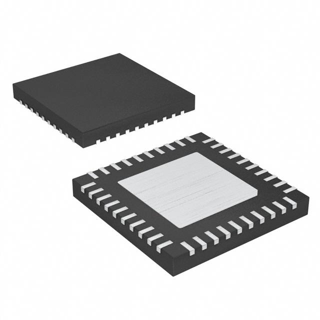


 工商网监
湘ICP备2023018690号
工商网监
湘ICP备2023018690号
