MAX1978/MAX1979
LE
AVAILAB
Integrated Temperature
Controllers for Peltier Modules
General Description
MAXIP
COMP
ITEC
39
37
38
MAXV
MAXIN
41
40
GND
GND
43
42
CTLI
VDD
45
44
CS
REF
47
46
OS1
48
+
36
OS2
N.C.
PGND2
LX2
PGND2
LX2
1
PVDD2
7
N.C.
LX2
PVDD2
SHDN
8
29
9
28
10
27
11
26
12
25
35
3
34
4
33
32
5
6
31
FREQ
N.C
PGND1
LX1
PGND1
LX1
PVDD1
N.C.
LX1
PVDD1
GND
GND
24
23
22
21
30
20
19
MAX1978
MAX1979
18
OT
2
BFBBFB+
AIN+
AINAOUT
Telecom Fiber Interfaces
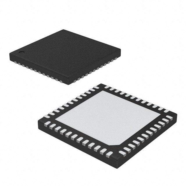
Pin Configurations appear at end of data sheet.
ATE
Functional
Diagrams continued at end of data sheet.
UCSP
is aOperating
trademarkCircuit
of Maxim
Integrated
Products,
Typical
appears
at end
of data Inc.
sheet.
TOP VIEW
17
EDFA Optical Amplifiers
Pin Configuration
16
Fiber Optic Network Equipment
MAX1979ETM+
-40°C to +85°C
48 Thin QFN-EP*
*EP = Exposed pad.
+Denotes a lead(Pb)-free/RoHS-compliant package.
DIFOUT
FBFB+
WDM, DWDM Laser-Diode Temperature Control
PIN-PACKAGE
48 Thin QFN-EP*
15
Fiber Optic Laser Modules
TEMP RANGE
-40°C to +85°C
14
Applications
PART
MAX1978ETM+
13
The MAX1978/MAX1979 are available in a low-profile
48-lead thin QFN-EP package and is specified over the
-40°C to +85°C temperature range. The thermally
enhanced QFN-EP package with exposed metal pad
minimizes operating junction temperature. An evaluation
kit is available to speed designs.
Ordering Information
UT
A chopper-stabilized instrumentation amplifier and a highprecision integrator amplifier are supplied to create a proportional-integral (PI) or proportional-integral-derivative (PID)
controller. The instrumentation amplifier can interface to an
external NTC or PTC thermistor, thermocouple, or semiconductor temperature sensor. Analog outputs are provided to
monitor TEC temperature
and current. In addition,
separate
Functional
Diagrams
overtemperature and undertemperature outputs indicate
when the TEC temperature is out of range. An on-chip voltage reference provides bias for a thermistor bridge.
INTOUT
INTGND
The MAX1978/MAX1979 are the smallest, safest, most
accurate complete single-chip temperature controllers for
Peltier thermoelectric cooler (TEC) modules. On-chip power
FETs and thermal control-loop circuitry minimize external
components while maintaining high efficiency. Selectable
500kHz/1MHz switching frequency and a unique ripple-cancellation scheme optimize component size and efficiency
while reducing noise. Switching speeds of internal
MOSFETs are optimized to reduce noise and EMI. An ultralow-drift chopper amplifier maintains ±0.001°C temperature
stability. Output current, rather than voltage, is directly controlled to eliminate current surges. Individual heating and
cooling current and voltage limits provide the highest level of
TEC protection.
The MAX1978 operates from a single supply and provides
bipolar ±3A output by biasing the TEC between the outputs
of two synchronous buck regulators. True bipolar operation
controls temperature without “dead zones” or other nonlinearities at low load currents. The control system does not
hunt when the set point is very close to the natural operating
point, where only a small amount of heating or cooling is
needed. An analog control signal precisely sets the TEC
current. The MAX1979 provides unipolar output up to 6A.
Features
o Smallest, Safest, Most Accurate Complete
Single-Chip Controller
o On-Chip Power MOSFETS—No External FETs
o Circuit Footprint < 0.93in2
o Circuit Height < 3mm
o Temperature Stability to 0.001°C
o Integrated Precision Integrator and Chopper
Stabilized Op Amps
o Accurate, Independent Heating and Cooling
Current Limits
o Eliminates Surges By Directly Controlling
TEC Current
o Adjustable Differential TEC Voltage Limit
o Low-Ripple and Low-Noise Design
o TEC Current Monitor
o Temperature Monitor
o Over- and Undertemperature Alarm
o Bipolar ±3A Output Current (MAX1978)
o Unipolar +6A Output Current (MAX1979)
TQFN-EP
*ELECTRICALLY CONNECTED TO THE UNDERSIDE METAL SLUG.
NOTE: GND IS CONNECTED TO THE UNDERSIDE METAL SLUG.
For pricing, delivery, and ordering information, please contact Maxim Direct
at 1-888-629-4642, or visit Maxim’s website at www.maximintegrated.com.
19-2490; Rev 3; 3/10
�MAX1978/MAX1979
Integrated Temperature
Controllers for Peltier Modules
ABSOLUTE MAXIMUM RATINGS
Peak LX Current (MAX1978) (Note 1).................................±4.5A
Peak LX Current (MAX1979) (Note 1)....................................+9A
Continuous Power Dissipation (TA = +70°C)
48-Lead Thin QFN-EP
(derate 26.3mW/°C above +70°C) (Note 2) .................2.105W
Operating Temperature Ranges
MAX1978ETM ..................................................-40°C to +85°C
MAX1979ETM ..................................................-40°C to +85°C
Maximum Junction Temperature .....................................+150°C
Storage Temperature Range .............................-65°C to +150°C
Lead Temperature (soldering, 10s) .................................+300°C
VDD to GND ..............................................................-0.3V to +6V
SHDN, MAXV, MAXIP, MAXIN,
CTLI, OT, UT to GND............................................-0.3V to +6V
FREQ, COMP, OS1, OS2, CS, REF, ITEC, AIN+, AIN-,
AOUT, INT-, INTOUT, BFB+, BFB-, FB+, FB-,
DIFOUT to GND......................................-0.3V to (VDD + 0.3V)
PVDD1, PVDD2 to VDD ...........................................-0.3V to +0.3V
PVDD1, PVDD2 to GND...............................-0.3V to (VDD + 0.3V)
PGND1, PGND2 to GND .......................................-0.3V to +0.3V
COMP, REF, ITEC, OT, UT, INTOUT, DIFOUT,
BFB-, BFB+, AOUT Short to GND .............................Indefinite
Note 1: LX has internal clamp diodes to PGND and PVDD. Applications that forward bias these diodes should not exceed the IC’s
package power dissipation limits.
Note 2: Solder underside metal slug to PCB ground plane.
Stresses beyond those listed under “Absolute Maximum Ratings” may cause permanent damage to the device. These are stress ratings only, and functional
operation of the device at these or any other conditions beyond those indicated in the operational sections of the specifications is not implied. Exposure to
absolute maximum rating conditions for extended periods may affect device reliability.
ELECTRICAL CHARACTERISTICS
(VDD = PVDD1 = PVDD2 = V SHDN = 5V, FREQ = GND, CTLI = FB+ = FB- = MAXV = MAXIP = MAXIN = REF, TA = 0°C to +85°C,
unless otherwise noted. Typical values at TA = +25°C.)
PARAMETER
Input Supply Range
SYMBOL
CONDITIONS
VDD
VDD = 5V, ITEC = 0 to ±3A,
VOUT = VOS1 - VOS2 (MAX1978)
Output Voltage Range
Maximum TEC Current
Reference Voltage
Reference Load Regulation
VOUT
ITEC(MAX)
VREF
∆VREF
VDD = 3V, ITEC = 0 to ±3A,
VOUT = VOS1 - VOS2 (MAX1978)
RDS(ON-P)
NFET Leakage
2
ILEAK(N)
UNITS
3.0
5.5
V
-4.3
+4.3
4.3
V
-2.3
+2.3
2.3
MAX1978
±3
MAX1979
6
VDD = 3V to 5.5V, IREF = 150µA
1.485
1.500
VMAXI_ = VREF
135
VMAXI_ = VREF/3
40
50
60
VMAXI_ = VREF
135
150
160
VMAXI_ = VREF/3
40
VDD = 3V to 5.5V, IREF = +10µA to -1mA
VOS1 > VCS
PFET On-Resistance
MAX
VDD = 3V, ITEC = 0 to 6A,
VOUT = VOS1 (MAX1979)
VOS1 < VCS
RDS(ON-N)
TYP
VDD = 5V, ITEC = 0 to 6A,
VOUT = VOS1 (MAX1979)
Current-Sense Threshold
NFET On-Resistance
MIN
A
1.515
V
1.2
5
mV
150
160
50
60
VDD = 5V, I = 0.5A
0.04
0.07
VDD = 3V, I = 0.5A
0.06
0.08
VDD = 5V, I = 0.5A
0.06
0.10
VDD = 3V, I = 0.5A
0.09
0.12
VLX = VDD = 5V, TA = +25°C
0.02
10
VLX = VDD = 5V, TA = +85°C
1
mV
Ω
Ω
µA
Maxim Integrated
�MAX1978/MAX1979
Integrated Temperature
Controllers for Peltier Modules
ELECTRICAL CHARACTERISTICS (continued)
(VDD = PVDD1 = PVDD2 = V SHDN = 5V, FREQ = GND, CTLI = FB+ = FB- = MAXV = MAXIP = MAXIN = REF, TA = 0°C to +85°C,
unless otherwise noted. Typical values at TA = +25°C.)
PARAMETER
PFET Leakage
No-Load Supply Current
Shutdown Supply Current
Thermal Shutdown
SYMBOL
TYP
MAX
VLX = 0, TA = +25°C
0.02
10
VLX = 0, TA = +85°C
1
IDD(NO
VDD = 5V
30
50
LOAD)
VDD = 3.3V
15
30
IDD-SD
SHDN = GND, VDD = 5V (Note 3)
2
3
ILEAK(P)
CONDITIONS
TSHUTDOWN Hysteresis = 15°C
165
UNITS
µA
mA
mA
°C
VDD rising
2.4
2.6
2.8
VDD falling
2.25
2.5
2.75
FREQ = GND
450
500
650
FREQ=VDD
800
1000
1200
IOS1, IOS2,
ICS
0 or VDD
-100
+100
µA
ISHDN,
IFREQ
0 or VDD
-5
+5
µA
0.25 ×
VDD
V
UVLO Threshold
VUVLO
Switching Frequency Internal
Oscillator
fSW-INT
OS1, OS2, CS Input Current
SHDN, FREQ Input Current
SHDN, FREQ Input Low Voltage
VIL
VDD = 3V to 5.5V
SHDN, FREQ Input High Voltage
VIH
VDD = 3V to 5.5V
MAXV Threshold Accuracy
MAXV, MAXIP, MAXIN
Input Bias Current
MIN
0.75 ×
VDD
kHz
V
VMAXV = VREF ✕ 0.67,
VOS1 to VOS2 = ±4V, VDD = 5V
-1
+1
VMAXV = VREF ✕ 0.33,
VOS1 to VOS2 = ±2V, VDD = 3V
-2
+2
-0.1
+0.1
IMAXV-BIAS,
VMAXV = VMAXI_ = 0.1V or 1.5V
IMAXI_-BIAS
V
%
µA
CTLI Gain
ACTLI
VCTLI = 0.5V to 2.5V (Note 4)
9.5
10
10.5
V/V
CTLI Input Resistance
RCTLI
1MΩ terminated at REF
0.5
1.0
2.0
MΩ
50
100
175
µS
Error Amp Transconductance
gm
ITEC Accuracy
ITEC Load Regulation
∆VITEC
Instrumentation Amp Input Bias
Current
IDIF-BIAS
Instrumentation Amp Offset
Voltage
VDIF-OS
Instrumentation Amp OffsetVoltage Drift with Temperature
Instrumentation Amp Preset
Gain
Maxim Integrated
VOS1 to VCS = +100mV or -100mV
-10
+10
%
VOS1 to VCS = +100mV or -100mV,
IITEC = ±10µA
-0.1
+0.1
%
VDD = 3V to 5.5V
-10
0
+10
nA
-200
+20
+200
µV
VDD = 3V to 5.5V
ADIF
RLOAD = 10kΩ to REF
0.1
45
50
µV/°C
55
V/V
3
�MAX1978/MAX1979
Integrated Temperature
Controllers for Peltier Modules
ELECTRICAL CHARACTERISTICS (continued)
(VDD = PVDD1 = PVDD2 = V SHDN = 5V, FREQ = GND, CTLI = FB+ = FB- = MAXV = MAXIP = MAXIN = REF, TA = 0°C to +85°C,
unless otherwise noted. Typical values at TA = +25°C.)
PARAMETER
Integrator Amp Open-Loop Gain
SYMBOL
AOL-INT
MIN
RLOAD = 10kΩ to REF
TYP
MAX
120
UNITS
dB
Integrator Amp CMRR
CMRRINT
Integrator Amp Input Bias Current
IINT-BIAS
VDD = 3V to 5.5V
Integrator Amp Voltage Offset
VINT-OS
VDD = 3V to 5.5V
Integrator Amp Gain Bandwidth
GBWINT
Undedicated Chopper Amp
Open-Loop Gain
AOL-AIN
Undedicated Chopper Amp
CMRR
CMRRAIN
Undedicated Chopper Amp Input
Bias Current
IAIN-BIAS
VDD = 3V to 5.5V
-10
0
+10
nA
Undedicated Chopper Amp
Offset Voltage
VAIN-OS
VDD = 3V to 5.5V
-200
+10
+200
µV
Undedicated Chopper Amp Gain
Bandwidth
GBWAIN
Undedicated Chopper Amp
Output Ripple
VRIPPLE
BFB_ Buffer Error
100
-3
RLOAD = 10kΩ to REF
A=5
+3
mV
100
kHz
120
dB
85
dB
100
kHz
20
mV
1
µA
Sinking 4mA
50
150
mV
UT Trip Threshold
FB+ - FB- (see Typical Application Circuit)
-20
mV
OT Trip Threshold
FB+ - FB- (see Typical Application Circuit)
20
mV
ILEAK
VOL
-200
+0.1
nA
+200
UT and OT Output Low Voltage
CLOAD < 100pF
dB
1
0
UT and OT Leakage Current
4
CONDITIONS
V UT = V OT = 5.5V
µV
Maxim Integrated
�MAX1978/MAX1979
Integrated Temperature
Controllers for Peltier Modules
ELECTRICAL CHARACTERISTICS
(VDD = PVDD1 = PVDD2 = V SHDN = 5V, FREQ = GND, CTLI = FB+ = FB- = MAXV = MAXIP = MAXIN = REF, TA = -40°C to +85°C,
unless otherwise noted.) (Note 5)
PARAMETER
Input Supply Range
SYMBOL
CONDITIONS
VDD
VDD = 5V, ITEC = 0 to ±3A,
VOUT = VOS1 -VOS2 (MAX1978)
Output Voltage Range
Maximum TEC Current
Reference Voltage
Reference Load Regulation
VOUT
ITEC(MAX)
VREF
∆VREF
VDD = 3V, ITEC = 0 to ±3A,
VOUT = VOS1 - VOS2 (MAX1978)
+4.3
4.3
V
-2.3
+2.3
MAX1978
±3
MAX1979
6
VDD = 3V to 5.5V, IREF = 150µA
1.475
VDD = 3V to 5.5V,
IREF = 10µA to -1mA
V
5
mV
VMAXI_ = VREF
135
VMAXI_ = VREF/3
40
160
60
VMAXI_ = VREF
135
160
VMAXI_ = VREF/3
40
60
50
LOAD)
VDD = 3.3V
30
IDD-SD
SHDN = GND, VDD = 5V (Note 3)
Switching Frequency Internal
Oscillator
fSW-INT
3
mV
mA
mA
VDD rising
2.4
2.8
VDD falling
2.25
2.75
FREQ = GND
450
650
FREQ = VDD
800
1200
-100
+100
µA
-5
+5
µA
0.25 ✕
VDD
V
IOS1, IOS2,
0 or VDD
ICS
I SHDN,
I FREQ
A
1.515
IDD(NO
VUVLO
0 or VDD
SHDN, FREQ Input Low Voltage
VIL
VDD = 3V to 5.5V
SHDN, FREQ Input High Voltage
VIH
VDD = 3V to 5.5V
Maxim Integrated
-4.3
VDD = 5V
UVLO Threshold
SHDN, FREQ Input Current
V
2.3
VOS1 > VCS
OS1, OS2, CS Input Current
UNITS
5.5
VDD = 3V, ITEC = 0 to 6A,
VOUT = VOS1 (MAX1979)
Current-Sense Threshold
Shutdown Supply Current
MAX
3
VDD = 5V, ITEC = 0 to 6A,
VOUT = VOS1 (MAX1979)
VOS1 < VCS
No-Load Supply Current
MIN
0.75 ✕
VDD
V
kHz
V
5
�MAX1978/MAX1979
Integrated Temperature
Controllers for Peltier Modules
ELECTRICAL CHARACTERISTICS (continued)
(VDD = PVDD1 = PVDD2 = V SHDN = 5V, FREQ = GND, CTLI = FB+ = FB- = MAXV = MAXIP = MAXIN = REF, TA = -40°C to +85°C,
unless otherwise noted.) (Note 5)
PARAMETER
SYMBOL
CONDITIONS
MIN
MAX
VMAXV = VREF 0.67,
VOS1 to VOS2 = ±4V, VDD = 5V
-1
+1
VMAXV = VREF ✕ 0.33, VOS1 to VOS2 = ±2V,
VDD = 3V
-2
+2
-0.1
+0.1
µA
10.5
V/V
✕
MAXV Threshold Accuracy
MAXV, MAXIP, MAXIN
Input Bias Current
IMAXV-BIAS,
VMAXV = VMAXI_ = 0.1V or 1.5V
IMAXI_-BIAS
UNITS
%
CTLI Gain
ACTLI
VCTLI = 0.5V to 2.5V (Note 4)
9.5
CTLI Input Resistance
RCTLI
1MΩ terminated at REF
0.5
2.0
MΩ
50
175
µS
-10
+10
%
-0.125
+0.125
%
-10
+10
nA
-200
+200
µV
45
55
V/V
Error Amp Transconductance
gm
ITEC Accuracy
VOS1 to VCS = +100mV or -100mV
ITEC Load Regulation
∆VITEC
Instrumentation Amp
Input Bias Current
IDIF-BIAS
Instrumentation Amp
Offset Voltage
VDIF-OS
Instrumentation Amp
Preset Gain
ADIF
VOS1 to VCS = +100mV or
-100mV, IITEC = ±10µA
VDD = 3V to 5.5V
RLOAD = 10kΩ to REF
Integrator Amp Input Bias Current
IINT-BIAS
VDD = 3V to 5.5V
1
nA
Integrator Amp Voltage Offset
VINT-OS
VDD = 3V to 5.5V
-3
+3
mV
Undedicated Chopper Amp Input
Bias Current
IAIN-BIAS
VDD = 3V to 5.5V
-10
+10
nA
Undedicated Chopper Amp
Offset Voltage
VAIN-OS
VDD = 3V to 5.5V
-200
+200
µV
CLOAD < 100pF
-200
+200
µV
1
µA
150
mV
BFB_ Buffer Error
UT and OT Leakage Current
UT and OT Output Low Voltage
ILEAK
VOL
V UT = V OT = 5.5V
Sinking 4mA
Note 3: Includes power FET leakage.
Note 4: CTLI gain is defined as:
A CTLI = (VCTLI −VREF )
(VOSI −VCS )
Note 5: Specifications to -40°C are guaranteed by design, not production tested.
6
Maxim Integrated
�MAX1978/MAX1979
Integrated Temperature
Controllers for Peltier Modules
Typical Operating Characteristics
(VDD = 5V, VCTLI = 1V, VFREQ = GND, RTEC = 1Ω, circuit of Figure 1, TA = +25°C, unless otherwise noted.)
EFFICIENCY vs. TEC CURRENT
VDD = 3.3V
70
MAX1978 toc02
80
70
60
EFFICIENCY (%)
60
50
40
30
50
VOS1
100mV/div
AC-COUPLED
40
30
20
20
VOS1 - VOS1
50mV/div
RTEC = 0.855Ω
RTEC = 1.1Ω
10
10
VOS2
100mV/div
AC-COUPLED
0
0
0.5
1.0
1.5
2.0
0
2.5
0.5
1.0
1.5
2.5
2.0
TEC CURRENT (A)
TEC CURRENT (A)
INPUT SUPPLY RIPPLE
TEC CURRENT vs. CTLI VOLTAGE
400ns/div
ZERO-CROSSING TEC CURRENT
MAX1978 toc05
MAX1978 toc04
0
MAX1978 toc06
EFFICIENCY (%)
80
MAX1978 toc01
90
OUTPUT-VOLTAGE
RIPPLE WAVEFORMS
MAX1978 toc03
EFFICIENCY vs. TEC CURRENT
VDD = 5V
VCTLI
200mV/div
1.5V
VCTLI
1V/div
VDD
20mV/div
AC-COUPLED
-0V
-0A
1ms/div
VITEC vs. TEC CURRENT
TEC CURRENT vs. TEMPERATURE
SWITCHING FREQUENCY
vs. TEMPERATURE
ITEC (A)
2.0
1.5
1.000
1.0
0.995
0.5
ITEC = 1A
RSENSE = 0.68Ω
0
0.990
-1
0
1
TEC CURRENT (A)
Maxim Integrated
2
3
MAX1978 toc09
508
506
SWITCHING FREQUENCY (kHz)
MAX1978 toc08
MAX1978 toc07
1.010
1.005
VITEC (V)
0A
20ms/div
2.5
-2
ITEC
500mA/div
200ns/div
3.0
-3
ITEC
2A/div
504
502
500
498
496
VCTLI = 1.5V
RTEC = 1Ω
494
492
-40
-20
0
20
40
TEMPERATURE (°C)
60
80
-40
-20
0
20
40
60
80
TEMPERATURE (°C)
7
�MAX1978/MAX1979
Integrated Temperature
Controllers for Peltier Modules
Typical Operating Characteristics (continued)
(VDD = 5V, VCTLI = 1V, VFREQ = GND, RTEC = 1Ω, circuit of Figure 1, TA = +25°C, unless otherwise noted.)
SWITCHING FREQUENCY CHANGE
vs. INPUT SUPPLY
-5
-10
-15
-20
-25
-30
0
-0.5
-1.0
-1.5
-2.0
-2.5
-3.0
-35
3.5
3.0
4.0
4.5
5.0
MAX1978 toc12
1
0
-1
-2
-3
-4
3.0
5.5
2
3.5
4.0
4.5
5.0
5.5
-40
-20
0
20
40
60
80
VDD (V)
TEMPERATURE (°C)
REFERENCE LOAD REGULATION
ATO VOLTAGE
vs. THERMISTOR TEMPERATURE
STARTUP AND SHUTDOWN WAVEFORMS
0.4
MAX1978 toc14
MAX1978 toc13
4.5
NTC, 10kΩ THERMISTOR
CIRCUIT IN FIGURES 1 AND 2
4.0
MAX1978 toc15
VDD (V)
0.6
VSHDN
5V/div
3.5
ATO VOLTAGE (V)
0.2
0
-0.2
-0.4
-0.6
SINK
SOURCE
3.0
2.5
ITEC
500mA/div
2.0
1.5
1.0
-0.8
IDD
200mA/div
0.5
-1.0
0
0
0.2
0.4
0.6
0.8
1.0
-10
0
10
20
30
40
50
REFERENCE LOAD CURRENT (mA)
THERMISTOR TEMPERATURE (°C)
CTLI STEP RESPONSE
INPUT SUPPLY STEP RESPONSE
VCTLI
1V/div
100µs/div
60
THERMAL STABILITY,
COOLING MODE
VDD
2V/div
MAX1978 toc18
-0.2
MAX1978 toc16
-0.4
MAX1978 toc17
REFERENCE VOLTAGE CHANGE (mV)
0.5
3
REFERENCE VOLTAGE CHANGE (mV)
0
REFERENCE VOLTAGE CHANGE
vs. TEMPERATURE
MAX1978 toc11
5
1.0
REFERENCE VOLTAGE CHANGE (mV)
MAX1978 toc10
SWITCHING FREQUENCY CHANGE (kHz)
10
REFERENCE VOLTAGE CHANGE
vs. INPUT SUPPLY
1.5V
0V
ITEC
20mA/div
ITEC
1A/div
0A
1ms/div
8
1A
10ms/div
TEMPERATURE
0.001°C/div
ITEC = +25°C
TA = +45°C
4s/div
Maxim Integrated
�MAX1978/MAX1979
Integrated Temperature
Controllers for Peltier Modules
Typical Operating Characteristics (continued)
(VDD = 5V, VCTLI = 1V, VFREQ = GND, RTEC = 1Ω, circuit of Figure 1, TA = +25°C, unless otherwise noted.)
THERMAL STABILITY,
HEATING MODE
TTEC = +25°C
TA = +5°C
ITEC = +25°C
TA = +25°C
MAX1978 toc21
0.03
0.02
TEMPERATURE ERROR (°C)
MAX1978 toc19
TEMPERATURE
0.001°C/div
MPERATURE
0.001°C/div
TEMPERATURE ERROR
vs. AMBIENT TEMPERATURE
MAX1978 toc20
THERMAL STABILITY,
ROOM TEMPERATURE
0.01
0
-0.01
-0.02
-0.03
4s/div
4s/div
-20
-10
0
10
20
30
40
50
AMBIENT TEMPERATURE (°C)
Pin Description
PIN
NAME
FUNCTION
1
OS2
Output Sense 2. OS2 senses one side of the differential TEC voltage. OS2 is a sense point, not a power
output.
2, 8, 29,
35
N.C.
Not Internally Connected
3, 5
PGND2
4, 6, 9
LX2
7, 10
PVDD2
Power 2 Inputs. Must be same voltage as VDD. Connect all PVDD2 inputs together at the VDD power plane.
Bypass to PGND2 with a 10µF ceramic capacitor.
11
SHDN
Shutdown Control Input. Active-low shutdown control.
12
OT
Over-Temperature Alarm. Open-drain output pulls low if temperature feedback rises 20mV
(typically +1.5°C) above the set-point voltage.
13
UT
Under-Temperature Alarm. Open-drain output pulls low if temperature feedback falls 20mV
(typically +1.5°C) below the set-point voltage.
14
Power Ground 2. Internal synchronous rectifier ground connections. Connect all PGND pins together at
power ground plane.
Inductor 2 Connection. Connect all LX2 pins together. Connect LX2 to LX1 when using the MAX1979.
INTOUT Integrator Amp Output. Normally connected to CTLI.
15
INT-
Integrator Amp Inverting Input. Normally connected to DIFOUT through thermal-compensation network.
16, 25,
26, 42, 43
GND
Analog Ground. Connect all GND pins to analog ground plane.
17
DIFOUT Chopper-Stabilized Instrumentation Amp Output. Differential gain is 50 ✕ (FB+ - FB-).
18
FB-
Chopper-Stabilized Instrumentation Amp Inverting Input. Connect to thermistor bridge.
19
FB+
Chopper-Stabilized Instrumentation Amp Noninverting Input. Connect to thermistor bridge.
20
BFB-
Chopper-Stabilized Buffered FB- Output. Used to monitor thermistor bridge voltage.
21
BFB+
Chopper-Stabilized Buffered FB+ Output. Used to monitor thermistor bridge voltage.
22
AIN+
Undedicated Chopper-Stabilized Amplifier Noninverting Input
Maxim Integrated
9
�MAX1978/MAX1979
Integrated Temperature
Controllers for Peltier Modules
Pin Description (continued)
PIN
NAME
23
AIN-
24
AOUT
Undedicated Chopper-Stabilized Amplifier Output
27, 30
PVDD1
Power 1 Inputs. Must be same voltage as VDD. Connect all PVDD1 inputs together at the VDD power plane.
Bypass to PGND1 with a 10µF ceramic capacitor.
28, 31, 33
LX1
Inductor 1 Connection. Connect all LX1 pins together. Connect LX1 to LX2 when using the MAX1979.
Power Ground 1. Internal synchronous-rectifier ground connections. Connect all PGND pins together at
power ground plane.
32, 34
PGND1
36
FREQ
Switching-Frequency Select. Low = 500kHz, high = 1MHz.
ITEC
TEC Current Monitor Output. The ITEC output voltage is a function of the voltage across the TEC currentsense resistor. VITEC = 1.50V + (VOS1 - VCS) ✕ 8.
37
10
FUNCTION
Undedicated Chopper-Stabilized Amplifier Inverting Input
38
COMP
Current-Control Loop Compensation. For most designs, connect a 10nF capacitor from COMP to GND.
39
MAXIP
Maximum Positive TEC Current. Connect MAXIP to REF to set default positive current limit +150mV/RSENSE.
40
MAXIN
Maximum Negative TEC Current. Connect MAXIN to REF to set default negative current limit -150mV /
RSENSE. Connect MAXIN to MAXIP when using the MAX1979.
41
MAXV
Maximum Bipolar TEC Voltage. Connect an external resistive divider from REF to GND to set the maximum
voltage across the TEC. The maximum TEC voltage is 4 ✕ VMAXV.
44
VDD
Analog Supply Voltage Input. Bypass to GND with a 10µF ceramic capacitor.
45
CTLI
TEC Current-Control Input. Sets differential current into the TEC. Center point is 1.50V (no TEC current).
Connect to INTOUT when using the thermal control loop. ITEC = (VOS1 - VCS)/RSENSE = (VCTLI - 1.50)/(10 ✕
RSENSE). When (VCLTI - VREF) > 0, VOS2 > VOS1 > VCS.
46
REF
1.5V Reference Voltage Output. Bypass REF to GND with a 1µF ceramic capacitor.
47
CS
Current-Sense Input. The current through the TEC is monitored between CS and OS1. The maximum TEC
current is given by 150mV/RSENSE and is bipolar for the MAX1978. The MAX1979 TEC current is unipolar.
48
OS1
—
EP
Output Sense 1. OS1 senses one side of the differential TEC voltage. OS1 is a sense point, not a power
output.
Exposed Pad. Solder evenly to the PCB ground plane to maximize thermal performance.
Maxim Integrated
�MAX1978/MAX1979
Integrated Temperature
Controllers for Peltier Modules
Functional Diagram
ON
OFF
SHDN
FREQ
VDD
REF
1.5V
REFERENCE
MAXV
PVDD1
MAX VTEC =
VMAXV x 4
MAXIP
3V TO 5.5V
LX1
MAX ITEC = (VMAXIP/
VREF) x (0.15V/RSENSE)
MAX ITEC = (VMAXIN/
VREF) x (0.15V/RSENSE)
MAXIN
CS
ITEC
PWM CONTROL AND GATE DRIVE
PGND1
CS
RSENSE
OS1
OS1
OS2
REF
PVDD2
CTLI
VDD
COMP
LX2
MAX1978
GND
OT
PGND2
50R
REF + 1V
R
UT
REF
50R
R
REF - 1V
REF
BFB-
BFB+
INTOUT
Maxim Integrated
INT-
AIN-
AOUT
AIN+
DIFOUT
FB+
FB-
11
�MAX1978/MAX1979
Integrated Temperature
Controllers for Peltier Modules
Detailed Description
TEC temperature. The on-chip thermal-control circuitry
can be configured to achieve temperature control stability of 0.001°C. Figure 1 shows a typical TEC thermalcontrol circuit.
Power Stage
The power stage of the MAX1978/MAX1979
thermoelectric cooler (TEC) temperature controllers
consists of two switching buck regulators that operate
together to directly control TEC current. This configuration creates a differential voltage across the TEC, allowing bidirectional TEC current for controlled cooling and
heating. Controlled cooling and heating allow accurate
TEC temperature control within the tight tolerances of
laser driver specifications.
The voltage at CTLI directly sets the TEC current. The
internal thermal-control loop drives CTLI to regulate
Ripple Cancellation
Switching regulators like those used in the
MAX1978/MAX1979 inherently create ripple voltage on
each common-mode output. The regulators in the
MAX1978 switch in phase and provide complementary
in-phase duty cycles, so ripple waveforms at the differential TEC output are greatly reduced. This feature suppresses ripple currents and electrical noise at the TEC
to prevent interference with the laser diode while minimizing output capacitor filter size.
VDD
REF
10µF
10µF
1µF
10µF
0.01µF
VDD
SHDN
PVDD1
PVDD2
REF MAXV MAXIN MAXIP
COMP
UNDERTEMP
ALARM
OVERTEMP
ALARM
DC CURRENT
MONITOR
3µH
LX1
CS
UT
1µF
0.068Ω
OT
OS1
ITEC
20kΩ
1%
4.7µF
MAX1978
TEC
BFB80.6kΩ
1µF
THERMISTOR
VOLTAGE
MONITOR
AIN-
OS2
AOUT
3µH
LX2
1µF
AIN+
REF
69.8kΩ
1%
105kΩ
1%
CTLI
FREQ
GND
REF
PGND2 PGND1
INTOUT
THERMAL
FEEDBACK
FBDIFOUT FB+
INT-
10kΩ
100kΩ
100kΩ
0.047µF
10µF
0.47µF
20kΩ
1MΩ
Figure 1. MAX1978 Typical Application Circuit. Circuit is configured for both cooling and heating the NTC thermistor. Current flowing
from OS2 and OS1 is cooling.
12
Maxim Integrated
�MAX1978/MAX1979
Integrated Temperature
Controllers for Peltier Modules
Switching Frequency
FREQ sets the switching frequency of the internal oscillator. The oscillator frequency is 500kHz when FREQ =
GND. The oscillator frequency is 1MHz when FREQ =
VDD. The 1MHz setting allows minimum inductor and filter-capacitor values. Efficiency is optimized with the
500kHz setting.
Voltage and Current-Limit Settings
The MAX1978 and MAX1979 provide settings to limit
the maximum differential TEC voltage. Applying a voltage to MAXV limits the maximum voltage across the
TEC to ±(4 � VMAXV).
The MAX1978 also limits the maximum positive and
negative TEC current. The voltages applied to MAXIP
and MAXIN independently set the maximum positive
and negative output current limits. The MAX1979 controls TEC current in only one direction, so the maximum
current is set only with MAXIP. MAXIN must be connected to MAXIP when using the MAX1979.
Chopper-Stabilized Instrumentation
Amplifier
The MAX1978 and MAX1979 include a chopped input
instrumentation amplifier with a fixed gain of 50. An
external thermal sensor, typically a thermistor, is connected to one of the amp’s inputs. The other input is
connected to a voltage that represents the temperature
set point. This set point can be derived from a resistordivider network or DAC. The included instrumentation
amplifier provides low offset drift needed to prevent
temperature set-point drift with ambient temperature
changes. Temperature stability of 0.001°C can be
achieved over a 0°C to +50°C ambient temperarure
range by using the amplifier as in Figure 1. DIFOUT is
the instrumentation amplifier output and is proportional
to 50 times the difference between the set-point temperature and the TEC temperature. This difference is
commonly referred to as the “error signal”. For best
temperature stability, derive the set-point voltage from
the same reference that drives the thermistor (usually
the MAX1978/MAX1979 REF output). This is called a
“ratiometric” or “bridge” connection. The bridge connection optimizes stability by eliminating REF drift as an
error source. Errors at REF are nullified because they
affect the thermistor and set point equally.
The instrumentation amplifier utilizes a chopped input
scheme to minimize input offset voltage and drift. This
generates output ripple at DIFOUT that is equal to the
chop frequency. The DIFOUT peak-to-peak ripple
amplitude is typically 100mV but has no effect on temperature stability. DIFOUT ripple is filtered by the integrator in the following stage. The chopper frequency is
Maxim Integrated
derived from, and is synchronized to, the switching frequency of the power stage.
Integrator Amplifier
An on-chip integrator amplifier is provided on the
MAX1978/MAX1979. The noninverting terminal of the
amplifier is connected internally to REF. Connect an
appropriate network of resistors and capacitors between
DIFOUT and INT-, and connect INTOUT to CTLI for typical operation. CTLI directly controls the TEC current
magnitude and polarity. The thermal-control-loop dynamics are set by the integrator input and feedback components. See the Applications Information section for
details on thermal-loop compensation.
Current Monitor Output
ITEC provides a voltage output proportional to the TEC
current, ITEC (see the Functional Diagram):
VITEC = 1.5V + 8 � (VOS1 - VCS)
Over- and Under-Temperature Alarms
The MAX1978/MAX1979 provide open-drain status outputs that alert a microcontroller when the TEC temperature is over or under the set-point temperature. OT and
UT pull low when V(FB1+ - FB-) is more than 20mV. For a
typical thermistor connection, this translates to approximately 1.5°C error.
Reference Output
The MAX1978/MAX1979 include an on-chip 1.5V voltage reference accurate to 1% over temperature.
Bypass REF with 1µF to GND. REF can be used to bias
an external thermistor for temperature sensing as
shown in Figures 1 and 2. Note that the 1% accuracy of
REF does not limit the temperature stability achievable
with the MAX1978/MAX1979. This is because the thermistor and set-point bridge legs are intended to be driven ratiometrically by the same reference source (REF).
Variations in the bridge-drive voltage then cancel out
and do not generate errors. Consequently, 0.001°C stable temperature control is achievable with the
MAX1978/MAX1979 reference.
An external source can be used to bias the thermistor
bridge. For best accuracy, the common-mode voltage
applied to FB+ and FB- should be kept between 0.5V
and 1V, however the input range can be extended from
0.2V to VDD / 2 if some shift in instrumentation amp offset
(approximately -50µV/V) can be tolerated. This shift
remains constant with temperature and does not contribute to set-point drift.
13
�MAX1978/MAX1979
Integrated Temperature
Controllers for Peltier Modules
VDD
REF
10µF
10µF
1µF
10µF
0.01µF
VDD
SHDN
PVDD1
PVDD2
COMP
UNDERTEMP
ALARM
OVERTEMP
ALARM
DC CURRENT
MONITOR
UT
REF MAXV MAXIN MAXIP
LX1
LX2
CS
3µH
1µF
OT
0.03Ω
ITEC
OS1
20kΩ
1%
MAX1979
4.7µF
BFB80.6kΩ
1µF
THERMISTOR
VOLTAGE
MONITOR
AIN-
TEC
OS2
AOUT
AIN+
REF
69.8kΩ
1%
105kΩ
1%
CTLI
FREQ
GND
FB-
REF
THERMAL
FEEDBACK
FB+
PGND2 PGND1
INTOUT
INT-
DIFOUT
10kΩ
100kΩ
10µF
0.047µF
0.47µF
20kΩ
100kΩ
1MΩ
Figure 2. MAX1979 Typical Application Circuit. MAXIN sets the maximum TEC current circuit configured for cooling with NTC thermistor. Current always flow from CS and OS2.
Buffered Outputs, BFB+ and BFBBFB+ and BFB- output a buffered version of the voltage
that appears on FB+ and FB-, respectively. The buffers
are typically used in conjunction with the undedicated
chopper amplifier to create a monitor for the thermistor
voltage/TEC temperature (Figures 1 and 2). These
buffers are unity-gain chopper amplifiers and exhibit
output ripple. Each output can be either integrated or
filtered to remove the ripple content if necessary.
Undedicated Chopper-Stabilized Amplifier
ted but is intended to provide a temperature-proportional analog output. The thermistor voltage typically is
connected to the undedicated chopper amplifier
through the included buffers BFB+ and BFB-. Figure 3
shows how to configure the undedicated amplifier as a
thermistor voltage monitor. The output voltage at AOUT
is not precisely linear, because the thermistor is not linear. AOUT is also chopper stabilized and exhibits output ripple and can be either integrated or filtered to
remove the ripple content if necessary.
In addition to the chopper amplifiers at DIFOUT and
BFB_, the MAX1978/MAX1979 include an additional
chopper amplifier at AOUT. This amplifier is uncommit14
Maxim Integrated
�MAX1978/MAX1979
Integrated Temperature
Controllers for Peltier Modules
22µF to 100µF ceramic capacitor between the V DD
power plane and power ground. Insufficient supply
bypassing can result in supply bounce and degraded
accuracy.
REF
69.8kΩ
1%
Compensation Capacitor
Include a compensation capacitor to ensure currentpower control-loop stability. Select the capacitor so that
the unity-gain bandwidth of the current-control loop is
less than or equal to 10% the resonant frequency of the
output filter:
AIN+
105kΩ
1%
AOUT
80.6kΩ
1%
1µF
⎛g ⎞ ⎛
⎞
24 × RSENSE
CCOMP ≥ ⎜ m ⎟ × ⎜
⎟
⎝ fBW ⎠ ⎝ 2π × (RSENSE + RTEC ) ⎠
AINREF
MAX1978
MAX1979
x50
20kΩ
1%
BFB-
10kΩ
FBVSETPOINT
where:
fBW = unity-gain bandwidth frequency
gm = loop transconductance, typically 100µA/V
CCOMP = value of the compensation capacitor
RTEC = TEC series resistance
RSENSE = sense resistor
FB+
Setting Voltage and Current Limits
Figure 3. Thermistor Voltage Monitor
Design Procedure
Inductor Selection
Small surface-mount inductors are ideal for use with the
MAX1978/MAX1979. Select the output inductors so that
the LC resonant frequency of the inductance and the
output capacitance is less than 1/5 the selected switching frequency. For example, 3.0µH and 1µF have a resonance at 92kHz, which is adequate for 500kHz
operation.
¡
f LC=
1
2π LC
where:
fLC = resonant frequency of output filter.
Capacitor Selection
Filter Capacitors
Decouple each power-supply input (VDD, PVDD1, and
PVDD2) with a 10µF ceramic capacitor close to the supply pins. If long supply lines separate the source supply from the MAX1978/MAX1979, or if the source
supply has high output impedance, place an additional
Maxim Integrated
Consider TEC parameters to guarantee a robust
design. These parameters include maximum positive
current, maximum negative current, and the maximum
voltage allowed across the TEC. These limits should be
used to set MAXIP, MAXIN, and MAXV voltages.
Setting Max Positive and Negative TEC Current
MAXIP and MAXIN set the maximum positive and negative TEC currents, respectively. The default current limit
is ±150mV / RSENSE when MAXIP and MAXIN are connected to REF. To set maximum limits other than the
defaults, connect a resistor-divider from REF to GND to
set VMAXI_. Use resistors in the 10kΩ to 100kΩ range.
VMAXI_ is related to ITEC by the following equations:
VMAXIP = 10 (ITECP(MAX) � RSENSE)
VMAXIN = 10 (ITECN(MAX) � RSENSE)
where ITECP(MAX) is the maximum positive TEC current
and ITECN(MAX) is the maximum negative TEC current.
Positive TEC current occurs when CS is less than OS1:
ITEC � RSENSE = CS - OS1 when ITEC < 0.
ITEC � RSENSE = OS1 - CS when ITEC > 0.
15
�MAX1978/MAX1979
Integrated Temperature
Controllers for Peltier Modules
The MAX1979 controls the TEC current in only one
direction (unipolar). Set the maximum unipolar TEC current by applying a voltage to MAXIP. Connect MAXIN to
MAXIP when using the MAX1979. The equation for setting MAXIP is the same for the MAX1978 and
MAX1979. Do not exceed the positive or negative current-limit specifications on the TEC. Refer to the TEC
manufacturer’s data sheet for these limits.
FBREF
CREF
MAX1978
MAX1979
FB+
VTHERMISTOR
VSETPOINT
Setting Max TEC Voltage
Apply a voltage to MAXV to control the maximum differential TEC voltage. MAXV can vary from 0 to REF. The
voltage across the TEC is four times VMAXV and can be
positive or negative.
FBREF
|VOS1 - VOS2| = 4 � VMAXV
Use resistors from 10kΩ to 100kΩ to form a voltagedivider to set VMAXV.
Thermal-Control Loop
The MAX1978/MAX1979 provide all the necessary
amplifiers needed to create a thermal-control loop.
Typically, the chopper-stabilized instrumentation amplifier generates an error signal and the integrator amplifier is used to create a PID controller. Figure 4 shows an
example of a simple PID implementation. The error signal needed to control the loop is generated from the
difference between the set point and the thermistor
voltage. The desired set-point voltage can be derived
from a potentiometer, DAC, or other voltage source.
Figure 5 details the required connections. Connect the
output of the PID controller to CTLI. For details, see the
Applications Information section.
VTHERMISTOR
CREF
MAX1978
MAX1979
FB+
DAC
VSETPOINT
DIGITAL
INPUT
Figure 5. The Set Point can be Derived from a Potentiometer
or a DAC
Control Inputs/Outputs
TEC Current Control
The voltage at CTLI directly sets the TEC current. CTLI
typically is driven from the output of a temperature-control circuit CINTOUT. For the purposes of the following
equations, it is assumed that positive TEC current is
heating.
The transfer function relating current through the TEC
(ITEC) and VCTLI is given by:
C3
ITEC = (VCTLI - VREF) / (10 � RSENSE)
C1
R3
R1
C2
INT-
DIFOUT
INTOUT
R2
where VREF is 1.50V
and ITEC = (VOS1 - VCS) / RSENSE
VCTLI is centered around REF (1.50V). ITEC is zero when
VCTLI = 1.50V. When VCTLI > 1.50V, the MAX1978 is heating. Current flow is from OS2 to OS1. The voltages are:
VOS2 > VOS1 > VCS
REF
Figure 4. Proportional Integral Derivative Controller
16
when VCTLI < 1.50V, current flows from OS1 to OS2:
VOS2 < VOS1 < VCS
Maxim Integrated
�MAX1978/MAX1979
Integrated Temperature
Controllers for Peltier Modules
Shutdown Control
Drive SHDN low to place the MAX1978/MAX1979 in a
power-saving shutdown mode. When the MAX1978/
MAX1979 are in shutdown, the TEC is off (VOS1 and
VOS2 decay to GND) and input supply current lowers to
2mA (typ).
ITEC Output
ITEC is a status output that provides a voltage proportional to the actual TEC current. ITEC = REF when TEC
current is zero. The transfer function for the ITEC output:
VITEC = 1.50 + 8 � (VOS1 - VCS)
Use ITEC to monitor the cooling or heating current
through the TEC. The maximum capacitance that ITEC
can drive is 100pF.
Applications Information
The MAX1978/MAX1979 drive a thermoelectric cooler
inside a thermal-control loop. TEC drive polarity and
power are regulated to maintain a stable control temperature based on temperature information read from a
thermistor, or from other temperature-measuring
devices. Carefully selected external components can
achieve 0.001°C temperature stability. The MAX1978/
MAX1979 provide precision amplifiers and an integrator amplifier to implement the thermal-control loop
(Figures 1 and 2).
Connecting and Compensating the
Thermal-Control Loop
Typically, the thermal loop consists of an error amplifier
and proportional integral derivative controller (PID)
(Figure 4). The thermal response of the TEC module
must be understood before compensating the thermal
loop. In particular, TECs generally have stronger heating capacity than cooling capacity because of the
effects of waste heat. Consider this point when analyzing the TEC response.
Analysis of the TEC using a signal analyzer can ease
compensation calculations. Most TECs can be crudely
modeled as a two-pole system. The second pole potentially creates an oscillatory condition because of the
associated 180° phase shift. A dominant pole compensation scheme is not practical because the crossover
frequency (the point of the Bode plot where the gain is
zero dB) must be below the TEC’s first pole, often as
low as 0.02Hz. This requires an excessively large inte-
Maxim Integrated
grator capacitor and results in slow loop-transient
response. A better approach is to use a PID controller,
where two additional zeros are used to cancel the TEC
and integrator poles. Adequate phase margin can be
achieved near the frequency of the TEC’s second pole
when using a PID controller. The following is an example of the compensation procedure using a PID controller.
Figure 6 details a two-pole transfer function of a typical
TEC module. This Bode plot can be generated with a
signal analyzer driving the CTLI input of the
MAX1978/MAX1979, while plotting the thermistor voltage from the module. For the example module, the two
poles are at 0.02Hz and 1Hz.
The first step in compensating the control loop involves
selecting components R3 and C2 for highest DC gain.
Film capacitors provide the lowest leakage but can be
large. Ceramic capacitors are a good compromise
between low leakage and small size. Tantalum and
electrolytic capacitors have the highest leakage and
generally are not suitable for this application. The integrating capacitor, C2, and R3 (Figure 4) set the first
zero (fz1). The specific application dictates where the
first zero should be set. Choosing a very low frequency
results in a very large value capacitor. Set the first zero
frequency to no more than 8 times the frequency of the
lowest TEC pole. Setting the frequency more than 8
times the lowest pole results in the phase falling below
-135° and may cause instability in the system. For this
example, C2 = 10µF. Resistor R3 then sets the zero at
0.16Hz using the following equation:
fz1 =
1
2π × C2 × R3
This yields a value of R3 = 99.47kΩ. For our example,
use 100kΩ.
Next, adjust the gain for a crossover frequency for maximum phase margin near the TEC’s second pole. From
Figure 6, the TEC bode plot, approximately 30dB of
gain is needed to move the 0dB crossover point up to
1.5Hz. The error amplifier provides a fixed gain of 50,
or approximately 34dB. Therefore, the integrator needs
to provide -4dB of gain at 1.5Hz. C1 and R3 set the
gain at the crossover frequency.
C1 =
A
1
+ 2π × R3 × fC
C2
17
�MAX1978/MAX1979
Integrated Temperature
Controllers for Peltier Modules
where:
A = The gain needed to move the 0dB crossover point
up to the desired frequency. In this case, A = -4dB =
0.6.
fC = The desired crossover frequency, 1.5Hz in this
example.
C1 is found to be 0.58µF; use 0.47µF.
Next, the second TEC pole must be cancelled by
adding a zero. Canceling the second TEC pole provides maximum phase margin by adding positive
phase to the circuit. Setting a second zero (fz2) to at
least 1/5 the crossover frequency (1.5Hz/5 = 0.3Hz),
and a pole (fp1) to 5 times the crossover frequency or
higher (5 × 1.5Hz = 7.5Hz) ensures good phase margin,
while allowing for variation in the location of the TEC’s
second pole. Set the zero fz2 to 0.3Hz and calculate R2:
1
fz2 =
2π × C1× R2
where fz2 is the second zero.
R2 is calculated to be 1.1MΩ; use 1MΩ.
Now pole fp1 is added at least 5 times the crossover
frequency to terminate zero fz2.
Choose fp1 = 15Hz, find R1 using the following equation:
fp1 =
Resistor R1 is found to be 22kΩ, use 20kΩ
The final step is to terminate the first zero by setting the
rolloff frequency with a second pole, fp2. A good
choice is 2 times fp1.
Choose fp2 = 30Hz, find C3 using the following equation:
fp2 =
The example given is a good place to start when compensating the thermal loop. Different TEC modules
require individual testing to find their optimal compensation scheme. Other compensation schemes can be
used. The above procedure should provide good
results for the majority of optical modules.
COMPENSATED
TEC GAIN AND PHASE
-90
-60
-70
-80
0.001
-135
0.01
0.1
1
10
FREQUENCY (Hz)
Figure 6. Bode Plot of a Generic TEC Module
18
-180
100
80
70
60
50
40
30
20
10
0
-10
-20
-30
-40
-50
-60
-70
-80
0.001
90
45
0
-45
-90
PHASE (DEGREES)
-45
-30
-40
-50
GAIN (dB)
45
PHASE (DEGREES)
GAIN (dB)
90
0
1
2π × C3 × R3
where C3 is found to be 0.05µF, use 0.047µF.
Figure 7 displays the compensated gain and phase
plots for the above example.
TEC GAIN AND PHASE
40
30
20
10
0
-10
-20
1
2π × C1× R1
-135
0.01
0.1
1
10
-180
100
FREQUENCY (Hz)
Figure 7. Compensated Thermal-Control Loop Using the TEC
Module in Figure 6
Maxim Integrated
�MAX1978/MAX1979
Integrated Temperature
Controllers for Peltier Modules
Typical Operating Circuit
INPUT
3V TO 5.5V
VDD
PVDD-
LX1
PGND1
ON
CS
SHDN
OFF
OVERTEMP ALARM
OT
UNDERTEMP ALARM
UT
BFB-
OS1
MAX1978
TEC
OS2
ITEC = ±3A
LX2
PGND2
AIN-
TEMP MONITOR
REF
AOUT
FB+
TEC CURRENT MONITOR
ITEC
AIN+
NTC
VOLTAGE LIMIT
MAXV
HEATING CURRENT LIMIT
MAXIP
COOLING CURRENT LIMIT
MAXIN
FBOPTIONAL DAC
DAC
REF
Package Information
Chip Information
TRANSISTOR COUNT: 6023
PROCESS: BiCMOS
Maxim Integrated
For the latest package outline information and land patterns, go
to www.maxim-ic.com/packages. Note that a "+", "#", or "-" in
the package code indicates RoHS status only. Package drawings may show a different suffix character, but the drawing pertains to the package regardless of RoHS status.
PACKAGE TYPE
PACKAGE CODE
DOCUMENT NO.
48 TQFN-EP
T4877+6
21-0144
19
�MAX1978/MAX1979
Integrated Temperature Controller for
Peltier Modules
Revision History
REVISION
NUMBER
REVISION
DATE
DESCRIPTION
PAGES
CHANGED
0
7/02
Initial release
1
2/07
Updated the Ordering Information, Pin Description, and Package Information.
—
2
1/10
Revised the Pin Description and the Setting Max Positive and Negative TEC
Current section.
10, 16
3
3/10
Revised the Figure 1 and 2 captions, and the Voltage and Current-Limit Settings
section.
12–14
1, 9, 10, 19, 20, 21
Maxim cannot assume responsibility for use of any circuitry other than circuitry entirely embodied in a Maxim product. No circuit patent licenses are implied.
Maxim reserves the right to change the circuitry and specifications without notice at any time. The parametric values (min and max limits) shown in the Electrical
Characteristics table are guaranteed. Other parametric values quoted in this data sheet are provided for guidance.
20
© Maxim Integrated
Maxim Integrated 160 Rio Robles, San Jose, CA 95134 USA 1-408-601-1000
The Maxim logo and Maxim Integrated are trademarks of Maxim Integrated Products, Inc.
�


 工商网监
湘ICP备2023018690号
工商网监
湘ICP备2023018690号
