Click here for production status of specific part numbers.
MAXM15062 3.3V Output
Evaluation Kit
General Description
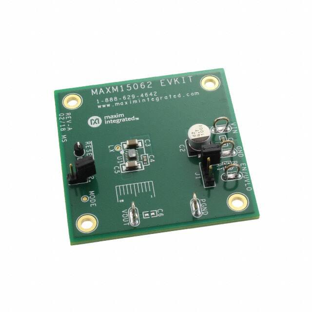
The MAXM15062 3.3V output evaluation kit (EV kit)
provides a proven design to evaluate the MAXM15062
high-voltage, high-efficiency, synchronous step-down
DC-DC module. The EV kit is programmed to deliver
3.3V output for loads up to 300mA. The EV kit features
an adjustable input undervoltage lockout, selectable
mode, and open-drain RESET signal. The MAXM15062
data sheet provides a complete description of the module
that should be read in conjunction with this EV kit data
sheet prior to modifying the demo circuit. For full module
features, benefits and parameters, refer to the MAXM15062
data sheet.
Features
●● Highly Integrated Solution
●● Wide 5.5V to 48V Input Range
●● Fixed 3.3V Output, Delivers Up To 300mA
Output Current
●● High 80.46% Efficiency
(VIN = 24V, VOUT = 3.3V at 150mA)
●● 500kHz Switching Frequency
●● ENABLE/UVLO Input, Resistor-Programmable UVLO
Threshold
●● PFM Feature for Better Light-Load Efficiency
●● Fixed Internal 4.1ms Soft-Start Time
●● RESET Output, with Pullup Resistor to VCC
●● Overcurrent and Overtemperature Protection
(OCP and OTP)
●● Low-Profile, Surface-Mount Components
●● Proven PCB Layout
●● Fully Assembled and Tested
●● Complies with CISPR22(EN55022) Class B
Conducted and Radiated Emissions
319-100325; Rev 0; 3/19
Evaluates: MAXM15062 3.3V
Output-Voltage Application
Quick Start
Recommended Equipment
●● One 4.5V to 60V, 300mA power supply
●● 1W resistive load with 300mA sink capacity
●● Four digital multimeters (DMM)
●● MAXM15062EVKIT#
Equipment Setup and Test Procedure
The EV kit is fully assembled and tested. Follow the steps
below to verify the board operation.
Caution: Do not turn on power supply until all
connections are completed.
1) Set the power supply at a voltage between 4.5V and
60V. Then, disable the power supply.
2) Connect the positive terminal of the power supply to
the VIN PCB pad and the negative terminal to the
nearest GND PCB pad. Connect the positive terminal of the 300mA load to the VOUT PCB pad and the
negative terminal to the nearest GND PCB pad.
3) Connect the DVM (DMM in voltage-measurement
mode) across the VOUT PCB pad and the nearest
GND PCB pad.
4) Verify that shunt is not installed on jumper J1
(see Table 1 for details).
5) Turn on the DC power supply.
6) Enable the load.
7) Verify that the DVM displays 3.3V.
Ordering Information appears at end of data sheet.
�Evaluates: MAXM15062 3.3V
Output-Voltage Application
MAXM15062 3.3V Output
Evaluation Kit
Detailed Description
Input Capacitor Selection
The MAXM15062 EV kit is designed to demonstrate
salient features of MAXM15062 power module. The EV kit
includes an EN/UVLO PCB pad, and jumper J1, to enable
the output at a desired input voltage. Jumper J2 allows
selection of either PWM or PFM mode of operation based
on light-load performance requirements. An additional
RESET pad is available for monitoring if the converter
output voltage is in regulation.
Output Capacitor Selection
X7R ceramic output capacitors are preferred due to their
stability over temperature in industrial applications. The
required output capacitor (C5) for 3.3V output is selected
from Table 1 of the MAXM15062 data sheet as 10µF/6.3V.
Fixed Output Voltage
The MAXM15062 is a fixed 3.3V output module. Connect
FB of MAXM15062 directly to VOUT for feedback control.
Enable/Undervoltage-Lockout (EN/UVLO)
Programming
The MAXM15062 offers an adjustable input undervoltagelockout feature. In this EV kit, for normal operation, leave
jumper J1 open. When J1 is left open, the MAXM15062 is
enabled when the input voltage rises above 5.4V. To disable MAXM15062, install a jumper across pins 2-3 on J1.
See Table 1 for J1 settings. A potential divider formed by
R1 and R2 sets the input voltage (VINU) at which the module is enabled. The value of resistor R1 is chosen to be
2.2MΩ, and R2 is calculated using the following equation:
R2 =
R 1 × 1.215
( VINU − 1.215 )
where R1 and R2 are in kΩ,
For MAXM15062 to turn on at 5.4V input, the Resistor R2
is calculated to be 634kΩ.
The input capacitor serves to reduce the current peaks
drawn from the input power supply and reduces switching
frequency ripple at the input. The input capacitance must
be greater than or equal to the value given in Table 1 of
MAXM15062 data sheet. Input capacitor C3 is chosen to
be 1µF/100V.
Electro-Magnetic Interference (EMI)
Compliance to conducted emissions (CE) standards
requires an EMI filter at the input of a switching power
converter. The EMI filter attenuates high-frequency currents drawn by the switching power converter, and limits
the noise injected back into the input power source.
Use of EMI filter components as shown in Figure 1 in
conjunction with the schematic results in lower conducted emissions, below CISPR22 Class B limits. The
MAXM15062 EV kit PCB layout is also designed to limit
radiated emissions from switching nodes of the power
converter, resulting in radiated emissions below CISPR22
Class B limits.
Hot-Plug-In and Long Input Cables
The MAXM15062 EV kit PCB provides an optional
electrolytic capacitor (C2, 4.7µF/100V) to dampen input
voltage peaks and oscillations that can arise during hotplug-in and/or due to long input cables. This capacitor
limits the peak voltage at the input of the MAXM15062
power module, when the EV kit is powered directly from a
precharged capacitive source or an industrial backplane
PCB. Long input cables, between input power source and
the EV kit circuit can cause input-voltage oscillations due
to the inductance of the cables. The equivalent series
resistance (ESR) of the electrolytic capacitor helps damp
out the oscillations caused by long input cables. Further,
capacitor C1 (0.1µF/100V), placed near the input of the
board, helps in attenuating high frequency noise.
Table 1. UVLO Enable/Disable Configuration (J1)
POSITION
EN/UVLO PIN
MAXM15062_ OUTPUT
Connected to the center node of resistor-divider
R1 and R2.
Programmed to startup at desired input-voltage
level.
1-2
Connected to VIN
Enabled if VIN is greater than VIN(MIN).
2-3
Connected to GND
Disabled
Not Installed*
*Default position
www.maximintegrated.com
Maxim Integrated │ 2
�Evaluates: MAXM15062 3.3V
Output-Voltage Application
MAXM15062 3.3V Output
Evaluation Kit
Mode of Operation
The MAXM15062 features PFM mode of operation to
increase the efficiency at light-load condition. If the MODE
pin is left unconnected during powerup, the module
operates in PFM mode at light loads. If the MODE pin is
connected to GND during power-up, the part operates in
constant-frequency PWM mode at all loads. See Table 2
for J2 settings.
VIN_EMI
L1
82µH
VIN_EMI
C7
0.1µF
VIN
C8
0.47µF
C9
1µF
Internal LDO
An internal regulator provides a 5V nominal supply to
power the internal functions of the module. The output of
the linear regulator (VCC) should be bypassed with a 1µF
capacitor C4 to GND.
Figure 1. EMI Filter Components
Table 2. Mode of Operation (J2)
POSITION
MODE PIN
1-2
Operates in PWM mode.
Not Installed*
Operates in PFM mode at light-load conditions.
*Default position
EV Kit Performance Report
STARTUP THROUGH ENABLE
VIN = 24V, VOUT = 3.3V, FULL LOAD, PWM MODE
EFFICIENCY vs. LOAD CURRENT
VOUT = 3.3V, PWM MODE
100
5V/div
EN/UVLO
90
80
80
20V/div
LX
2V/div
5V/div
VOUT
EFFICIENCY (%)
70
60
VIN = 5.5V
50
VIN = 12V
40
VIN = 24V
30
VIN = 36V
20
RESET
VIN = 48V
10
1ms/div
0
0
30
60
90 120 150 180 210 240 270 300
LOAD CURRENT (mA)
www.maximintegrated.com
EFFICIENCY vs. LOAD CURRENT
VOUT = 3.3V, PFM MODE
100
90
EFFICIENCY (%)
toc01
toc02
toc03
VIN = 5.5V
70
60
50
VIN = 36V
40
30
VIN = 12V
VIN = 48V
VIN = 24V
20
10
0
1
10
100
LOAD CURRENT (mA)
Maxim Integrated │ 3
�Evaluates: MAXM15062 3.3V
Output-Voltage Application
MAXM15062 3.3V Output
Evaluation Kit
EV Kit Performance Report (continued)
OUTPUT VOLTAGE vs. LOAD CURRENT
VOUT = 3.3V, PFM MODE
OUTPUT VOLTAGE vs. LOAD CURRENT
VOUT = 3.3V, PWM MODE
toc04
toc05
3.39
VIN = 36V
VIN = 5.5V
3.306
3.304
VIN = 12V
VIN = 24V
VIN = 48V
3.33
VIN = 48V
VIN = 12V
3.31
3.29
VIN = 24V
3.27
0
30
60
3.25
90 120 150 180 210 240 270 300
0
30
60
IOUT = 100mA
3.3060
3.3045
IOUT = 300mA
IOUT = 200mA
3.3030
3.3015
90 120 150 180 210 240 270 300
LOAD CURRENT (mA)
LOAD CURRENT (mA)
OUTPUT VOLTAGE RIPPLE
VIN = 24V, VOUT = 3.3V, FULL LOAD, PWM MODE
LOAD TRANSIENT RESPONSE
VIN = 24V, VOUT = 3.3V, PFM MODE
(LOAD CURRENT STEPPED FROM 5mA TO 150mA)
toc07
IOUT = 0A
3.3075
3.35
3.302
3.300
3.3090
VIN = 36V
3.37
OUTPUT VOLTAGE (V)
OUTPUT VOLTAGE (V)
3.308
VIN = 5.5V
OUTPUT VOLTAGE (V)
3.310
OUTPUT VOLTAGE vs. INPUT VOLTAGE
VOUT = 3.3V, PWM MODE
toc06
3.3000
10
0
20
40
30
50
INPUT VOLTAGE(V)
LOAD TRANSIENT RESPONSE
VIN = 24V, VOUT = 3.3V, PWM MODE
(LOAD CURRENT STEPPED FROM 150mA TO 300mA)
toc09
toc08
50mV/div
VOUT (AC)
VOUT (AC)
VOUT (AC)
100mV/div
10mV/div
100mA/div
IOUT
2µs/div
VIN = 24V, VOUT
CONDUCTED EMISSION PLOT
(EMI FILTER: C6, C7 = 0.1µF, C8 = 0.47µF,
L1 = 82µH, C9 = 1µF)
BODE PLOT
= 3.3V, FULL LOAD, PWM MODE
toc10
RADIATED EMISSION PLOT
(C6 = 0.1µF, C7, C8, C9 = OPEN, L1 = SHORT)
toc11
90
0
30
0
GAIN
-20
-30
-40
CROSSOVER FREQUENCY = 46.091kHz
PHASE MARGIN = 60.693°
-60
1k
10k
FREQUENCY (Hz)
www.maximintegrated.com
-60
-90
100k
MAGNITUDE (dBµV)
PHASE
20
PHASE MARGIN (⁰)
40
60
60
CISPR-22 CLASS B QP LIMIT
50
CISPR-22 CLASS B AVG LIMIT
40
PEAK
EMISSION
30
20
10
0
AVERAGE
EMISSION
10M
1M
FREQUENCY(Hz)
CONDITIONS : VIN = 24V, VOUT = 3.3V, IOUT = 0.3A
150k
50
MAGNITUDE (dBµV/m)
60
toc12
70
70
60
GAIN (dB)
100µs/div
100µs/div
80
-80
IOUT
100mA/div
CISPR-22 CLASS B QP LIMIT
40
30
VERTICAL
SCAN
20
10
0
-10
HORIZONTAL
SCAN
100M
1G
FREQUENCY(Hz)
CONDITIONS : VIN = 24V, VOUT = 3.3V, IOUT = 0.3A
30M
Maxim Integrated │ 4
�Evaluates: MAXM15062 3.3V
Output-Voltage Application
MAXM15062 3.3V Output
Evaluation Kit
Ordering Information
Component Suppliers
PART
TYPE
MAXM15062EVKIT#
EV Kit
#Denotes RoHS compliant.
SUPPLIER
WEBSITE
Murata Americas
www.murata.com
NEC TOKIN America, Inc.
www.nec-tokinamerica.com
Panasonic Corp.
www.panasonic.com
SANYO Electric Co., Ltd.
www.sanyodevice.com
TDK Corp.
www.component.tdk.com
TOKO America, Inc.
www.tokoam.com
Note: Indicate that you are using the MAXM15062 when
contacting these component suppliers.
MAXM15062 3.3V EV Kit Bill of Materials
ITEM
QTY
DESIGNATION
DESCRIPTION
MANUFACTURER
PARTNUMBER-1
1
1
C1
0.1µF±10%,100V,
X7R ceramic capacitor (0603)
MURATA GRM188R72A104KA35
2
1
C2
4.7µF±20%,100V,
Aluminimum Capacitor
NICHICON UUR2A4R7MCL6GS
3
1
C3
1µF±10%,100V,
X7R ceramic capacitor (1206)
MURATA GRM31CR72A105KA01L
TDK C3216X7R2A105K160
4
1
C4
1µF±10%,16V,
X7R ceramic capacitor (0603)
MURATA GRM188R71C105KA12
TDK C1608X7R1C105K
5
1
C5
10µF±10%,6.3V,
X7R ceramic capacitor (1206)
MURATA GRM31CR70J106K
6
1
C6
OPEN (OPTIONAL : 0.1µF ±10%,
50V, X7R ceramic capacitor (0603))
Murata GRM188R71H104KA93
7
1
R1
2.2MΩ ±1% resistor (0402)
VISHAY DALE CRCW04022M20FK
8
1
R2
634kΩ ±1% resistor (0402)
VISHAY DALE CRCW0402634KFK
9
1
R3
100kΩ ±1% resistor (0402)
VISHAY DALE CRCW0402100KFK
10
1
U1
MAXM15062,
10-pin micro-SLIC Power Module
MAXIM MAXM15062AMB+T
11
1
L1
OPTIONAL : 82µH Shielded
Wirewound Inductor(2016)
Murata LQH2MPN820MGRL
12
1
C7
OPTIONAL : 0.1µF ±10%,100V,
X7R ceramic capacitor (0603)
MURATA GRM188R72A104KA35
13
1
C8
OPTIONAL : 0.47µF±10%,100V,
X7R ceramic capacitor (1206)
Murata GRM31MR72A474KA35L
14
1
C9
1µF±10%,100V,
X7R ceramic capacitor (1206)
MURATA GRM31CR72A105KA01L
www.maximintegrated.com
MANUFACTURER
PARTNUMBER-2
YAGEO PHICOMP RC0402FR-07100KL
TDK C3216X7R2A105K160
Maxim Integrated │ 5
�MODE
EN/UVLO
GND
C1
0.1UF
100V
VIN
4.7UF
100V
C2
1
+
2
VIN
J2
J1
C3
1UF
100V
1
3
1
2
2
VCC
C4
1UF
16V
R2
634K
R1
2.2M
7
4
8
GND
VCC
MODE
EN/UVLO
VIN
10
2
www.maximintegrated.com
9
VIN
3
RESET
LX
6
FB
OUT
5
LX
1
U1
MAXM15062
100K
R3
VCC
C5
10UF
6.3V
VOUT
C6
OPEN
RESET
PGND
VOUT
MAXM15062 3.3V Output
Evaluation Kit
Evaluates: MAXM15062 3.3V
Output-Voltage Application
MAXM15062 3.3V EV Kit Schematic
Maxim Integrated │ 6
�Evaluates: MAXM15062 3.3V
Output-Voltage Application
MAXM15062 3.3V Output
Evaluation Kit
MAXM15062 3.3V EV Kit PCB Layout Diagrams
1.0’’
MAXM15062 EV Kit PCB Layout—Silk Top
1.0’’
MAXM15062 EV Kit PCB Layout—Top Layer
www.maximintegrated.com
Maxim Integrated │ 7
�Evaluates: MAXM15062 3.3V
Output-Voltage Application
MAXM15062 3.3V Output
Evaluation Kit
MAXM15062 3.3V EV Kit PCB Layout Diagrams (continued)
1.0’’
MAXM15062 EV Kit PCB Layout—Layer 2 Ground
1.0’’
MAXM15062 EV Kit PCB Layout—Layer 3 Power
www.maximintegrated.com
Maxim Integrated │ 8
�Evaluates: MAXM15062 3.3V
Output-Voltage Application
MAXM15062 3.3V Output
Evaluation Kit
MAXM15062 3.3V EV Kit PCB Layout Diagrams (continued)
1.0’’
MAXM15062 EV Kit PCB Layout—Bottom Layer
www.maximintegrated.com
Maxim Integrated │ 9
�Evaluates: MAXM15062 3.3V
Output-Voltage Application
MAXM15062 3.3V Output
Evaluation Kit
Revision History
REVISION
NUMBER
REVISION
DATE
0
3/19
DESCRIPTION
Initial release
PAGES
CHANGED
—
For pricing, delivery, and ordering information, please visit Maxim Integrated’s online storefront at https://www.maximintegrated.com/en/storefront/storefront.html.
Maxim Integrated cannot assume responsibility for use of any circuitry other than circuitry entirely embodied in a Maxim Integrated product. No circuit patent licenses
are implied. Maxim Integrated reserves the right to change the circuitry and specifications without notice at any time.
Maxim Integrated and the Maxim Integrated logo are trademarks of Maxim Integrated Products, Inc.
© 2019 Maxim Integrated Products, Inc. │ 10
�


 工商网监
湘ICP备2023018690号
工商网监
湘ICP备2023018690号
