19-0887; Rev 5; 7/04
+5V, +10V Precision
Voltage References
Features
The REF01/REF02 are industry-standard precision voltage references. The stable 10V output of the REF01
can be adjusted over a ±3% range with minimal effect
on temperature stability, while the 5V output REF02 can
be adjusted over a ±6% range. The 10V REF01 has a
single-supply operation over an input voltage range of
13V to 33V, while the 5V REF02 has a single-supply
operation over an input voltage range of 7V to 33V.
Both devices offer a low-current drain of 1mA. The
REF02 also provides a TEMP pin whose output voltage
varies linearly with temperature, making this device
suitable for a wide variety of temperature-sensing and
control applications. For new designs, refer to the
MAX6035 or MAX6143 data sheets.
♦ Pretrimmed to +5V, +10V ±0.3%
♦ Excellent Temperature Stability: 3ppm/°C
♦ Low Noise: 10µVP-P (REF02)
♦ Low Supply Current: 1.4mA (max)
♦ Short-Circuit Protected
♦ Linear Temperature Transducer Output (REF02)
Ordering Information
TEMP RANGE
MAX TEMPCO
(ppm/°C)
INITIAL ERROR
(mV)
REF01EP
0°C to +70°C
8.5
±30
8 Plastic DIP
REF01HP
0°C to +70°C
25
±50
8 Plastic DIP
REF01HSA
0°C to +70°C
25
±50
8 SO
REF01CP
0°C to +70°C
65
±100
8 Plastic DIP
REF01CSA
0°C to +70°C
65
±100
8 SO
PART
REF01CESA
PIN-PACKAGE
-40°C to +85°C
65
±100
8 SO
REF02EP
0°C to +70°C
8.5
±15
8 Plastic DIP
REF02HP
0°C to +70°C
25
±25
8 Plastic DIP
REF02HSA
0°C to +70°C
25
±25
8 SO
REF02CP
0°C to +70°C
65
±50
8 Plastic DIP
REF02CSA
0°C to +70°C
65
±50
8 SO
-40°C to +85°C
65
±50
8 SO
REF02CESA
Ordering Information continued at end of data sheet.
Applications
Typical Operating Circuit
Analog-to-Digitial Converters
+15V
Digitial-to-Analog Converters
2
Digital Voltmeters
VIN
VO
6
OUTPUT
Voltage Regulators
Threshold Detectors
REF01
REF02 TRIM 5
RP
10kΩ
GND
4
REFERENCE WITH TRIMMED OUTPUT.
________________________________________________________________ Maxim Integrated Products
For pricing, delivery, and ordering information, please contact Maxim/Dallas Direct! at
1-888-629-4642, or visit Maxim’s website at www.maxim-ic.com.
1
REF01/REF02
General Description
�REF01/REF02
+5V, +10V Precision
Voltage References
ABSOLUTE MAXIMUM RATINGS–REF01
Input Voltage
REF01, A, E, H.....................................................................40V
REF01C ...............................................................................30V
Continuous Power Dissipation
T099 (J) (derate at 7.1mW°C above +80°C).................500mW
CERDIP (2) (derate at 6.7mW/°C above +75°C) .........500mW
Plastic Dip (P) (derate at 5.6mW/°C above +36°C) .....500mW
Small Outline (S) (derate at 5.0mW/°C above +55°C) ..300mW
Output Short-Circuit Duration
(to ground or VIN) .......................................................Indefinite
Storage Temperature Range .............................-65°C to +150°C
Operating Temperature Range
REF01A, REF01 ..............................................-55°C to +125°C
REF01E, REF01H, REF01C
(except REF01CESA)...........................................0°C to +70°C
REF01CESA ......................................................-40°C to +85°C
Lead Temperature (soldering, 60s) .................................+300°C
Stresses beyond those listed under “Absolute Maximum Ratings” may cause permanent damage to the device. These are stress ratings only, and functional
operation of the device at these or any other conditions beyond those indicated in the operational sections of the specifications is not implied. Exposure to
absolute maximum rating conditions for extended periods may affect device reliability.
ELECTRICAL CHARACTERISTICS—REF01/REF01A/REF01E/REF01H
(VIN = +15V, TA = +25°C, unless otherwise noted.)
PARAMETER
Output Voltage
SYMBOL
VO
MAX
MIN
TYP
MAX
IL = 0
9.97
10.00
10.03
9.95
10.00
10.05
V
±3.0
±3.3
±3.0
±3.3
∆Vtrim
RP = 10kΩ
enP-P
0.1Hz to 10Hz (Note 1)
30
20
30
µVP-P
VIN = 13V to 33V (Note 2)
0.006
0.010
0.006
0.010
%/V
0.008
0.006
0.010
%/mA
1.4
mA
IL = 0 to 10mA (Note 2)
0.005
tON
To ±0.1% of final value
400
Quiescent Supply Current
ISY
No load
1.0
Load Current
IL
Sink Current
IS
To specified output
voltage tolerance
ISC
%
20
Turn-On Settling Time
Short-Circuit Current
UNITS
TYP
Output Voltage Noise
Load Regulation
REF01/REF01H
MIN
Output Adjustment Range
Line Regulation
REF01A/REF01E
CONDITIONS
To specified output
voltage tolerance
400
1.4
µs
1.0
10
21
10
21
mA
0.3
0.5
0.3
0.5
mA
30
mA
VO = 0V
30
ELECTRICAL CHARACTERISTICS—REF01/REF01A/REF01E/REF01H
(VIN = +15V, -55°C ≤ TA ≤ +125°C for REF01A and REF01, 0°C ≤ TA ≤ +70°C for REF01E and REF01H, IL = 0mA, unless otherwise
noted.)
REF01A/REF01E
PARAMETER
SYMBOL
UNITS
MIN
Output Voltage Change with
Temperature (Note 3)
∆VOT
Output Voltage Temperature
Coefficient
TCVO
REF01/REF01H
CONDITIONS
TYP
MAX
0°C ≤ TA ≤ +70°C
0.02
-55°C ≤ TA ≤ +125°C
(Note 4)
MIN
TYP
MAX
0.06
0.07
0.17
0.06
0.15
0.18
0.45
3
8.5
10.0
25.0
%
ppm/°C
Change in VO Temperature
Coefficient with Output
Adjustment
RP = 10kΩ
Line Regulation
0°C ≤ TA ≤ +70°C
0.007
0.012
0.007
0.012
(VIN = 13V to 33V) (Note 2)
-55°C ≤ TA ≤ +125°C
0.009
0.015
0.009
0.015
Load Regulation
(IL = 0 to 8mA) (Note 2)
0°C ≤ TA ≤ +70°C
0.006
0.010
0.007
0.012
-55°C ≤ TA ≤ +125°C
0.007
0.012
0.009
0.015
2
0.7
0.7
_______________________________________________________________________________________
ppm/%
%/V
%/mA
�+5V, +10V Precision
Voltage References
REF01/REF02
ELECTRICAL CHARACTERISTICS—REF01C
(VIN = +15V, TA = +25°C, IL = 0mA, unless otherwise noted.)
PARAMETER
SYMBOL
Output Voltage
VO
CONDITIONS
MAX
IL = 0mA
9.90
10.00
10.10
V
±2.7
±3.3
25
35
µVP-P
VIN = 13V to 30V (Note 2)
0.009
0.015
%/V
IL = 0 to 8mA
0.006
0.015
IL = 0 to 4mA
0.006
0.015
∆Vtrim
RP = 10kΩ
Output Voltage Noise
enP-P
0.1Hz to 10Hz (Note 1)
Load Regulation (Note 2)
UNITS
TYP
Output Adjustment Range
Line Regulation
REF01C
MIN
Turn-On Settling Time
tON
To ±0.1% of final value
Quiescent Supply Current
ISY
No load
%
400
1.0
%/mA
µs
1.6
mA
Load Current
IL
To specified output voltage tolerance
8
21
mA
Sink Current
IS
To specified output voltage tolerance
0.2
0.5
mA
30
mA
Short-Circuit Current
ISC
VO = 0V
ELECTRICAL CHARACTERISTICS—REF01C
(VIN = +15V, TA = TMIN to TMAX, unless otherwise noted.)
PARAMETER
SYMBOL
REF01C
CONDITIONS
MIN
Output Voltage Change with
Temperature
Output Voltage Temperature
Coefficient
Change in VO Temperature
Coefficient with Output Adjustment
UNITS
TYP
MAX
∆VOT
(Note 3)
0.14
0.45
%
TCVO
(Note 4)
20
65
ppm/°C
RP = 10kΩ
0.7
ppm/%
Line Regulation
VIN = 13V to 30V (Note 2)
0.011
0.018
%/V
Load Regulation
IL = 0 to 5mA (Note 2)
0.008
0.018
%/mA
Note 1: Guaranteed by design for REF01EP, REF01HP, REF01HSA, REF01CP, REF01CSA, REF01CESA. Sample tested for all other
grades and packages.
Note 2: Line and load regulation specifications include the effect of self heating. REF01EP, REF01HP, REF01HSA, REF01CP, REF01CSA,
REF01CESA are 100% production tested at TA = +25°C and guaranteed by design for TA = TMIN to TMAX, as specified.
Note 3: ∆VOT is defined as the absolute difference between the maximum output voltage and the minimum output voltage over the
specified temperature range expressed as a percentage of 10V. REF01CP, REF01CSA, REF01CESA, REF01HSA guaranteed
by design.
-V
⎡V
⎤
∆VOT = ⎢ MAX MIN ⎥ × 100
10V
⎣
⎦
Note 4: TCVO is defined as ∆VOT divided by the temperature range. REF01CP, REF01CSA, REF01CESA, REF01HSA guaranteed by
design.
Output Adjustment
The REF01 trim terminal can be used to adjust the voltage over a 10V ±300mV range. This feature allows the
system designer to trim system errors by setting the reference to a voltage other than 10V, including 10.240V for
binary applications (see the Typical Operating Circuit).
Adjustment of the output does not significantly affect the
temperature performance of the device. The temperature coefficient change is approximately 0.7ppm/°C for
100mV of output adjustment.
_______________________________________________________________________________________
3
�REF01/REF02
+5V, +10V Precision
Voltage References
ABSOLUTE MAXIMUM RATINGS–REF02
Input Voltage
REF02, A, E, H.....................................................................40V
REF02C, D...........................................................................30V
Continuous Power Dissipation
T099 (J) (derate at 7.1mW°C above +80°C).................500mW
CERDIP (2) (derate at 6.7mW/°C above +75°C) .........500mW
Plastic Dip (P) (derate at 5.6mW/°C above +36°C) .....500mW
Small Outline (S) (derate at 5.0mW/°C above +55°C) ..300mW
Storage Temperature Range .............................-65°C to +150°C
Operating Temperature Range
REF02A, REF02 ..............................................-55°C to +125°C
REF02E, REF02H .................................................0°C to +70°C
REF02C (except REF02CESA), REF02D .............0°C to +70°C
REF02CESA ......................................................-40°C to +85°C
Output Short-Circuit Duration
(to ground or VIN) .......................................................Indefinite
Lead Temperature (soldering, 60s) .................................+300°C
Stresses beyond those listed under “Absolute Maximum Ratings” may cause permanent damage to the device. These are stress ratings only, and functional
operation of the device at these or any other conditions beyond those indicated in the operational sections of the specifications is not implied. Exposure to
absolute maximum rating conditions for extended periods may affect device reliability.
ELECTRICAL CHARACTERISTICS—REF02/REF02A/REF02E/REF02H
(VIN = +15V, TA = +25°C, unless otherwise noted.)
PARAMETER
Output Voltage
SYMBOL
VO
IL = 0
Output Adjustment Range
∆Vtrim
RP = 10kΩ
Output Voltage Noise
enP-P
0.1Hz to 10Hz (Note 5)
Line Regulation
Load Regulation
REF02A/REF02E
CONDITIONS
REF02/REF02H
UNITS
MIN
TYP
MAX
MIN
TYP
MAX
4.985
5.000
5.015
4.975
5.000
5.025
V
±3
±6
±3
±6
%
10
15
10
15
µVP-P
VIN = 8V to 33V (Note 6)
0.006
0.010
0.006
0.010
%/V
0.010
0.006
0.010
%/mA
1.4
mA
IL = 0 to 10mA (Note 6)
0.005
Turn-On Settling Time
tON
To ±0.1% of final value
230
Quiescent Supply Current
ISY
No load
1.0
230
1.4
µs
1.0
Load Current
IL
To specified output voltage tolerance
10
21
10
21
mA
Sink Current
IS
To specified output voltage tolerance
0.3
0.5
0.3
0.5
mA
Short-Circuit Current
Temperature Voltage
Output
ISC
VO = 0V
30
30
mA
VT
(Note 7)
630
630
mV
ELECTRICAL CHARACTERISTICS—REF02/REF02A/REF02E/REF02H
(VIN = +15V, -55°C ≤ TA ≤ +125°C for REF02A and REF02, 0°C ≤ TA ≤ +70°C for REF02E and REF02H, IL = 0mA, unless otherwise
noted.)
REF02A/REF02E
PARAMETER
SYMBOL
UNITS
MIN
Output Voltage Change with
Temperature (Note 8)
Output Voltage Temperature
Coefficient
Change in VO Temperature
Coefficient with Output
∆VOT
TCVO
REF02/REF02H
CONDITIONS
TYP
MAX
0°C ≤ TA ≤ +70°C
0.02
-55°C ≤ TA ≤ +125°C
0.06
3
(Note 9)
RP = 10kΩ
TYP
MAX
0.06
0.07
0.17
0.15
0.18
0.45
8.5
10
25
0.7
MIN
0.7
%
ppm/°C
ppm/%
Adjustment
0°C ≤ TA ≤ +70°C
0.007
0.012
0.007
0.012
-55°C ≤ TA ≤ +125°C
0.009
0.015
0.009
0.015
Load Regulation
0°C ≤ TA ≤ +70°C
0.006
0.010
0.007
0.012
(IL = 0 to 8mA) (Note 6)
-55°C ≤ TA ≤ +125°C
0.007
0.012
0.009
0.015
Line Regulation
(VIN = 8V to 33V) (Note 6)
4
_______________________________________________________________________________________
%/V
%/mA
�+5V, +10V Precision
Voltage References
(VIN = +15V, -55°C ≤ TA ≤ +125°C for REF02A and REF02, 0°C ≤ TA ≤ +70°C for REF02E and REF02H, IL = 0mA, unless otherwise
noted.)
REF02A/REF02E
PARAMETER
SYMBOL
UNITS
MIN
Temperature Voltage Output
Temperature Coefficient
TCVT
REF02/REF02H
CONDITIONS
TYP
(Note 7)
MAX
MIN
2.1
TYP
MAX
2.1
mV/°C
ELECTRICAL CHARACTERISTICS—REF02C/REF02D
(VIN = +15V, TA = +25°C, unless otherwise noted.)
PARAMETER
SYMBOL
Output Voltage
VO
Output Adjustment Range
Output Voltage Noise
∆Vtrim
enP-P
Line Regulation
Load Regulation (Note 6)
REF02C
CONDITIONS
REF02D
UNITS
MIN
TYP
MAX
MIN
TYP
MAX
IL = 0mA
4.950
5.000
5.050
4.900
5.000
5.100
RP = 10kΩ
±2.7
±6.0
±2.0
±6.0
%
18
12
µVP-P
0.010
0.04
0.015
0.04
0.1Hz to 10Hz
12
(Note 5)
VIN = 8V to 30V (Note 6)
0.009
0.015
IL = 0 to 8mA
0.006
0.015
IL = 0 to 4mA
Turn-On Settling Time
tON
To ±0.1% of final value
230
Quiescent Supply Current
ISY
No load
1.0
230
1.6
1.0
V
%/V
%/mA
µs
2.0
mA
Load Current
IL
To specified output
voltage tolerance
8
21
8
21
mA
Sink Current
IS
To specified output
voltage tolerance
0.2
0.5
0.2
0.5
mA
Short-Circuit Current
ISC
VO = 0V
30
30
mA
Temperature Voltage Output
VT
(Note 7)
630
630
mV
ELECTRICAL CHARACTERISTICS—REF02C/REF02D
(VIN = +15V, TA = TMIN to TMAX, IL = 0mA, unless otherwise noted.)
REF02C
PARAMETER
SYMBOL
UNITS
MIN
Output Voltage Change with
Temperature
Output Voltage Temperature
Coefficient
REF02D
CONDITIONS
TYP
MAX
MIN
TYP
MAX
∆VOT
(Note 8)
0.14
0.45
0.49
1.7
%
TCVO
(Note 9)
20
65
70
250
ppm/°C
RP = 10kΩ
0.7
Change in VO Temperature
Coefficient with Output
Adjustment
0.7
ppm/%
Line Regulation
VIN = 8V to 30V (Note 6)
0.011
0.018
0.012
0.05
%/V
Load Regulation
IL = 0 to 5mA (Note 6)
0.008
0.018
0.016
0.05
%/mA
Temperature Voltage Output
Temperature Coefficient
TCVT
(Note 7)
2.1
2.1
mV/°C
_______________________________________________________________________________________
5
REF01/REF02
ELECTRICAL CHARACTERISTICS—REF02/REF02A/REF02E/REF02H (continued)
�ELECTRICAL CHARACTERISTICS–REF02 (continued)
(VIN = +15V, TA = TMIN to TMAX, IL = 0mA, unless otherwise noted.)
Note 5: Guaranteed by design for REF02EP, REF02HP, REF02HSA, REF02CP, REF02CSA, REF02CESA. Sample tested for all
other grades and packages.
Note 6: Line and load regulation specifications include the effect of self heating. REF02EP, REF02HP, REF02HSA, REF02CP, REF02CSA,
REF02CESA are 100% production tested at TA = +25°C and guaranteed by design for TA = TMIN to TMAX, as specified.
Note 7: Limit current in or out of pin 3 to 50nA and capacitance on pin 3 to 30pF.
Note 8: ∆VOT is defined as the absolute difference between the maximum output voltage and the minimum output voltage over the
specified temperature range expressed as a percentage of 5V. REF02CP, REF02CSA, REF02CESA, REF02HSA guaranteed
by design.
-V
⎡V
⎤
∆VOT = ⎢ MAX MIN ⎥ × 100
5V
⎣
⎦
Note 9: TCVO is defined as ∆VOT divided by the temperature range. REF02CP, REF02CSA, REF02CESA, REF02HSA guaranteed by
design.
Output Adjustment
880
The REF02 trim terminal can be used to adjust the output voltage over a 5V ±300mV range. This feature
allows the system designer to trim system errors by setting the reference to a voltage other than 5V (refer to
the Typical Operating Circuit).
Adjustment of the output does not significantly affect
the temperature performance of the device. Typically,
the temperature coefficient change is 0.7ppm/°C for
100mV of output adjustment.
Temperature Voltage Output
The REF02 provides a temperature-dependent output
voltage on the TEMP pin. This voltage is proportional to
the absolute temperature, and has a scale factor of
approximately 2.1mV/°C (Figure 1).
830
TEMP VOLTAGE OUTPUT (mV)
REF01/REF02
+5V, +10V Precision
Voltage References
780
730
680
630
580
530
480
430
-60 -40 -20
0 20 40 60 80 100 120 140
TEMPERATURE (°C)
Figure 1. REF02 Temperature/Voltage Output vs. Temperature
Output Voltage = 2.1(T + 273)mV
where T = Temperature in °C.
6
_______________________________________________________________________________________
�+5V, +10V Precision
Voltage References
56
46
36
26
10,000
VIN = 15V
TA = +25°C
OUTPUT NOISE (µVP-P)
VIN = 15V
TA = +25°C
1000
100
REF01/02 TOC03
10,000
REF01/02 TOC02
VIN = 15V
TA = +25°C
OUTPUT NOISE (µVP-P)
LINE REGULATION (dB)
REF01/02 TOC01
76
66
REF02 OUTPUT WIDEBAND
NOISE vs. BANDWIDTH
(0.1Hz TO FREQUENCY INDICATED)
REF01 OUTPUT WIDEBAND
NOISE vs. BANDWIDTH
(0.1Hz TO FREQUENCY INDICATED)
LINE REGULATION
vs. FREQUENCY
1000
100
16
6
100
1k
10k
100k
1M
1k
10k
100k
10
1M
1k
10k
100k
MAXIMUM LOAD CURRENT
vs. INPUT VOLTAGE
NORMALIZED LOAD
REGULATION (∆IL = 10mA)
vs. TEMPERATURE
NORMALIZED LINE REGULATION
vs. TEMPERATURE
15
10
1.3
1.2
1.1
1.0
0.9
0.8
1.4
1.3
0
15
20
25
1.1
1.0
0.9
0.8
0.6
0.6
30
1.2
0.7
0.7
TA = +25°C
-60 -40 -20
0
-60 -40 -20
20 40 60 80 100 120 140
0
20 40 60 80 100 120 140
TEMPERATURE (°C)
MAXIMUM LOAD CURRENT
vs. TEMPERATURE
QUIESCENT CURRENT
vs. TEMPERATURE
OUTPUT CHANGE DUE TO
THERMAL SHOCK
15
10
5
VIN = 15V
1.2
1.1
1.0
0.9
0.8
0
0
20 40 60 80 100 120 140
TEMPERATURE (°C)
VIN = 15V
0.030
0.025
TA = TA =
+25°C +75°C
0.020
0.015
0.010
DEVICE IMMERSED
IN +75°C OIL BATH
0.005
0
0.7
-60 -40 -20
0.035
PERCENT CHANGE OUTPUT VOLTAGE (%)
20
REF01/02 TOC08
25
1.3
QUIESCENT CURRENT (mA)
VIN = 15V
REF01/02 TOC09
TEMPERATURE (°C)
REF01/02 TOC07
INPUT VOLTAGE (V)
30
1M
REF01/02 TOC06
VIN = 15V
LOAD REG (T)/LOAD REG (+25°C)
500mW MAXIMUM
DISSIPATION
20
REF01/02 TOC05
SHORT-CIRCUIT
PROTECTION
1.4
LOAD REG (T)/LOAD REG (+25°C)
30
10
100
FREQUENCY (Hz)
REF01/02 TOC04
MAXIMUM LOAD CURRENT (mA)
100
FREQUENCY (Hz)
5
MAXIMUM LOAD CURRENT (mA)
10
FREQUENCY (Hz)
35
25
10
10
10
-60 -40 -20
0
20 40 60 80 100 120 140
TEMPERATURE (°C)
-10
0
10
20
30
40
50
60
TIME (s)
_______________________________________________________________________________________
7
REF01/REF02
Typical Operating Characteristics
(TA = +25°C, unless otherwise noted.)
�+5V, +10V Precision
Voltage References
REF01/REF02
Typical Applications
+15V
1.1mA
2
2
6
VIN
VIN
VO
+10V
VO
6
+
10kΩ
REF01
9V
REF01
TRIM
GND
5
100kΩ 10.000V
TRIM
+15V
4
4
-10V
OP-07
5kΩ
GND
9V
10kΩ
5
-15V
-
Figure 2. Precision Calibration Standard
Figure 3. ±10V Reference
+15V
2
+15V
2
VIN
VO
VIN
VO
6
REF02
TRIM
REF02
3
TRIM
GND
4
IOUT
VREF 9.09kΩ
6
5
R
IOUT =
5.0V
+ 1mA
R
5.11kΩ
5
50kΩ
1.5kΩ
1.5kΩ
±5%
7
8
4
*
4
200kΩ
*UP TO 10 FEET OF SHIELDED
4-CONDUCTOR CABLE.
Figure 4. Current Source
6
OP-07
3
TEMP
GND
2
Figure 5. Precision Temperature Transducer with
Remote Sensor
_______________________________________________________________________________________
-15V
VOUT
(10mV/°C)
�+5V, +10V Precision
Voltage References
PART
TEMP RANGE
MAX TEMPCO
INITIAL ERROR
PIN-PACKAGE
REF01AJ*
-55°C to +125°C
8.5
±30
8 TO-99
REF01AZ*
-55°C to +125°C
8.5
±15
8 Hermetic DIP
REF01CJ*
0°C to +70°C
65
±100
8 TO-99
REF01CP-2*
0°C to +70°C
65
±100
8 Plastic DIP
REF01CZ*
0°C to +70°C
65
±100
8 CERDIP
REF01EJ*
0°C to +70°C
8.5
±30
8 TO-99
REF01EZ*
0°C to +70°C
8.5
±30
8 CERDIP
REF01HF*
0°C to +70°C
25
±50
8 TO-99
REF01HZ*
0°C to +70°C
25
±50
8 Hermetic DIP
REF01J*
-55°C to +125°C
25
±50
8 TO-99
REF01Z*
-55°C to +125°C
25
±50
8 CERDIP
REF02AJ*
-55°C to +125°C
8.5
±15
8 TO-99
REF02AZ*
-55°C to +125°C
8.5
±15
8 Hermetic DIP
REF02CJ*
0°C to +70°C
65
±50
8 TO-99
REF02CZ*
0°C to +70°C
65
±50
8 CERDIP
REF02DJ*
0°C to +70°C
25
±100
8 TO-99
REF02DP*
0°C to +70°C
25
±100
8 Plastic DIP
REF02DSA*
0°C to +70°C
25
±100
8 SO
REF02EJ*
0°C to +70°C
8.5
±15
8 TO-99
REF02EZ*
0°C to +70°C
8.5
±15
8 CERDIP
REF02HJ*
0°C to +70°C
25
±25
8 TO-99
REF02HZ*
0°C to +70°C
25
±25
8 Hermetic DIP
REF02J*
-55°C to +125°C
25
±25
8 TO-99
REF02Z*
-55°C to +125°C
25
±25
8 CERDIP
*Not recommended for new designs. Contact factory for availability.
Pin Configurations
N.C.
TOP VIEW
N.C.
8
1
VIN 2
N.C./TEMP*
7
8
N.C.
N.C. 1
8
N.C.
VIN 2
7
N.C.
VIN 2
7
N.C.
6
VOUT
5
TRIM
N.C./TEMP*
5
4
GROUND
(CASE)
N.C. 1
6 VOUT
REF01/
REF02
3
N.C.
TRIM
3
REF01/
REF02
GND 4
6
VOUT
5
TRIM
N.C./TEMP*
DIP
3
REF01/
REF02
GDN 4
SO
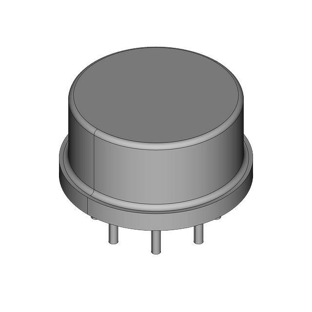
TO-99 METAL CAN
*NOTE: PIN 3 IS N.C. (NO CONNECTION) ON REF01, TEMP OUTPUT ON REF02.
Package Information
For the latest package outline information, go to
www.maxim-ic.com/packages.
Maxim cannot assume responsibility for use of any circuitry other than circuitry entirely embodied in a Maxim product. No circuit patent licenses are
implied. Maxim reserves the right to change the circuitry and specifications without notice at any time.
Maxim Integrated Products, 120 San Gabriel Drive, Sunnyvale, CA 94086 408-737-7600 _____________________ 9
© 2004 Maxim Integrated Products
Printed USA
is a registered trademark of Maxim Integrated Products.
REF01/REF02
Ordering Information (continued)
�


 工商网监
湘ICP备2023018690号
工商网监
湘ICP备2023018690号
