±0.5°C Accurate PWM
Temperature Sensor in 5-Lead SC-70
TMP05/TMP06
FEATURES
FUNCTIONAL BLOCK DIAGRAM
VDD
5
TMP05/TMP06
TEMPERATURE
SENSOR
Σ-Δ
CORE
REFERENCE
CONV/IN 2
3 FUNC
4
GND
Isolated sensors
Environmental control systems
Computer thermal monitoring
Thermal protection
Industrial process control
Power-system monitors
The TMP05/TMP06 are monolithic temperature sensors that
generate a modulated serial digital output (PWM), which varies
in direct proportion to the temperature of the devices. The high
period (TH) of the PWM remains static over all temperatures,
while the low period (TL) varies. The B Grade version offers a
high temperature accuracy of ±1°C from 0°C to 70°C with
excellent transducer linearity. The digital output of the TMP05/
TMP06 is CMOS-/TTL-compatible and is easily interfaced to
the serial inputs of most popular microprocessors. The flexible
open-drain output of the TMP06 is capable of sinking 5 mA.
The TMP05/TMP06 are specified for operation at supply voltages
from 3 V to 5.5 V. Operating at 3.3 V, the supply current is
typically 370 μA. The TMP05/TMP06 are rated for operation
over the –40°C to +150°C temperature range. It is not recommended to operate these devices at temperatures above 125°C
for more than a total of 5% (5,000 hours) of the lifetime of the
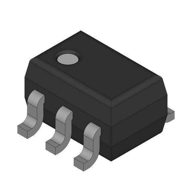
devices. They are packaged in low cost, low area SC-70 and
SOT-23 packages.
The TMP05/TMP06 have three modes of operation: continuously converting mode, daisy-chain mode, and one shot mode.
1 OUT
OUTPUT
CONTROL
CLK AND
TIMING
GENERATION
APPLICATIONS
GENERAL DESCRIPTION
AVERAGING
BLOCK/
COUNTER
03340-001
Modulated serial digital output, proportional to
temperature
±0.5°C typical accuracy at 25°C
±1.0°C accuracy from 0°C to 70°C
Two grades available
Operation from −40°C to +150°C
Operation from 3 V to 5.5 V
Power consumption 70 μW maximum at 3.3 V
CMOS-/TTL-compatible output on TMP05
Flexible open-drain output on TMP06
Small, low cost, 5-lead SC-70 and SOT-23 packages
Figure 1.
A three-state FUNC input determines the mode in which the
TMP05/TMP06 operate.
The CONV/IN input pin is used to determine the rate at which
the TMP05/TMP06 measure temperature in continuously
converting mode and one shot mode. In daisy-chain mode, the
CONV/IN pin operates as the input to the daisy chain.
PRODUCT HIGHLIGHTS
1.
The TMP05/TMP06 have an on-chip temperature sensor
that allows an accurate measurement of the ambient
temperature. The measurable temperature range is
–40°C to +150°C.
2.
Supply voltage is 3 V to 5.5 V.
3.
Space-saving 5-lead SOT-23 and SC-70 packages.
4.
Temperature accuracy is typically ±0.5°C. Each part needs
a decoupling capacitor to achieve this accuracy.
5.
Temperature resolution of 0.025°C.
6.
The TMP05/TMP06 feature a one shot mode that reduces
the average power consumption to 102 μW at 1 SPS.
Rev. B
Information furnished by Analog Devices is believed to be accurate and reliable. However, no
responsibility is assumed by Analog Devices for its use, nor for any infringements of patents or other
rights of third parties that may result from its use. Specifications subject to change without notice.
No license is granted by implication or otherwise under any patent or patent rights of Analog
Devices.Trademarks and registered trademarks are the property of their respective owners.
One Technology Way, P.O. Box 9106, Norwood, MA 02062-9106, U.S.A.
Tel: 781.329.4700
www.analog.com
Fax: 781.461.3113
©2006 Analog Devices, Inc. All rights reserved.
�TMP05/TMP06
TABLE OF CONTENTS
Features .............................................................................................. 1
Converter Details ....................................................................... 13
Applications....................................................................................... 1
Functional Description.............................................................. 13
Functional Block Diagram .............................................................. 1
Operating Modes........................................................................ 13
General Description ......................................................................... 1
TMP05 Output ........................................................................... 16
Product Highlights ........................................................................... 1
TMP06 Output ........................................................................... 16
Revision History ............................................................................... 2
Application Hints ........................................................................... 17
Specifications..................................................................................... 3
Thermal Response Time ........................................................... 17
TMP05A/TMP06A Specifications ............................................. 3
Self-Heating Effects.................................................................... 17
TMP05B/TMP06B Specifications .............................................. 5
Supply Decoupling ..................................................................... 17
Timing Characteristics ................................................................ 7
Layout Considerations............................................................... 18
Absolute Maximum Ratings............................................................ 8
Temperature Monitoring........................................................... 18
ESD Caution.................................................................................. 8
Daisy-Chain Application........................................................... 18
Pin Configuration and Function Descriptions............................. 9
Continuously Converting Application .................................... 24
Typical Performance Characteristics ........................................... 10
Outline Dimensions ....................................................................... 26
Theory of Operation ...................................................................... 13
Ordering Guide .......................................................................... 26
Circuit Information.................................................................... 13
REVISION HISTORY
4/06—Rev. A to Rev. B
Changes to Table 1............................................................................ 3
Changes to Table 2............................................................................ 5
Changes to Table 8.......................................................................... 14
Changes to Table 9.......................................................................... 15
10/05—Rev. 0 to Rev. A
Changes to Specifications Table...................................................... 3
Changes to Absolute Maximum Ratings ....................................... 8
Changes to Figure 4.......................................................................... 8
Changes to Figure 7........................................................................ 10
Changes to Figure 15...................................................................... 11
Deleted Figure 18............................................................................ 12
Changes to One Shot Mode Section ............................................ 14
Changes to Figure 20...................................................................... 14
Changes to Daisy-Chain Mode Section ...................................... 15
Changes to Figure 23...................................................................... 15
Changes to Equation 5 and Equation 7 ....................................... 17
Added Layout Considerations Section ........................................ 18
Updated Outline Dimensions....................................................... 26
Changes to Ordering Guide .......................................................... 26
8/04—Revision 0: Initial Version
Rev. B | Page 2 of 28
�TMP05/TMP06
SPECIFICATIONS
TMP05A/TMP06A SPECIFICATIONS
All A grade specifications apply for −40°C to +150°C, VDD decoupling capacitor is a 0.1 μF multilayer ceramic, TA = TMIN to TMAX,
VDD = 3.0 V to 5.5 V, unless otherwise noted.
Table 1.
Parameter
TEMPERATURE SENSOR AND ADC
Nominal Conversion Rate (One Shot Mode)
Accuracy @ VDD = 3.0 V to 5.5 V
Temperature Resolution
TH Pulse Width
TL Pulse Width
Quarter Period Conversion Rate
(All Operating Modes)
Accuracy
@ VDD = 3.3 V (3.0 V to 3.6 V)
@ VDD = 5 V (4.5 V to 5.5 V)
Temperature Resolution
TH Pulse Width
TL Pulse Width
Double High/Quarter Low Conversion Rate
(All Operating Modes)
Accuracy
@ VDD = 3.3 V (3.0 V to 3.6 V)
@ VDD = 5 V (4.5 V to 5.5 V)
Temperature Resolution
TH Pulse Width
TL Pulse Width
Long-Term Drift
Temperature Hysteresis
SUPPLIES
Supply Voltage
Supply Current
Normal Mode 2
@ 3.3 V
@ 5.0 V
Quiescent2
@ 3.3 V
@ 5.0 V
One Shot Mode @ 1 SPS
Power Dissipation
1 SPS
Min
Typ
Max
Unit
Test Conditions/Comments
±2
±3
±4
±5 1
°C
°C
°C
°C
°C/5 μs
ms
ms
See Table 7
TA = 0°C to 70°C, VDD = 3.0 V to 5.5 V
TA = –40°C to +100°C, VDD = 3.0 V to 5.5 V
TA = –40°C to +125°C, VDD = 3.0 V to 5.5 V
TA = –40°C to +150°C, VDD = 3.0 V to 5.5 V
Step size for every 5 μs on TL
TA = 25°C, nominal conversion rate
TA = 25°C, nominal conversion rate
0.025
40
76
See Table 7
±1.5
±1.5
0.1
10
19
°C
°C
°C/5 μs
ms
ms
TA = –40°C to +150°C
TA = –40°C to +150°C
Step size for every 5 μs on TL
TA = 25°C, QI conversion rate
TA = 25°C, QP conversion rate
See Table 7
±1.5
±1.5
0.1
80
19
0.081
0.0023
3
°C
°C
°C/5 μs
ms
ms
°C
°C
TA = –40°C to +150°C
TA = –40°C to +150°C
Step size for every 5 μs on TL
TA = 25°C, DH/QL conversion rate
TA = 25°C, DH/QL conversion rate
Drift over 10 years, if part is operated at 55°C
Temperature cycle = 25°C to 100°C to 25°C
5.5
V
370
425
600
650
μA
μA
Nominal conversion rate
Nominal conversion rate
3
5.5
30.9
12
20
μA
μA
μA
Device not converting, output is high
Device not converting, output is high
Average current @ VDD = 3.3 V,
nominal conversion rate @ 25°C
Average current @ VDD = 5.0 V,
nominal conversion rate @ 25°C
VDD = 3.3 V, continuously converting at
nominal conversion rates @ 25°C
Average power dissipated for VDD = 3.3 V,
one shot mode @ 25°C
Average power dissipated for VDD = 5.0 V,
one shot mode @ 25°C
37.38
μA
803.33
μW
101.9
μW
186.9
μW
Rev. B | Page 3 of 28
�TMP05/TMP06
Parameter
TMP05 OUTPUT (PUSH-PULL) 3
Output High Voltage (VOH)
Output Low Voltage (VOL)
Output High Current (IOUT) 4
Pin Capacitance
Rise Time (tLH) 5
Fall Time (tHL)5
RON Resistance (Low Output)
TMP06 OUTPUT (OPEN DRAIN)3
Output Low Voltage (VOL)
Output Low Voltage (VOL)
Pin Capacitance
High Output Leakage Current (IOH)
Device Turn-On Time
Fall Time (tHL) 6
RON Resistance (Low Output)
DIGITAL INPUTS3
Input Current
Input Low Voltage (VIL)
Input High Voltage (VIH)
Pin Capacitance
Min
Typ
Max
VDD − 0.3
0.4
2
10
50
50
55
0.4
1.2
10
0.1
20
30
55
5
±1
0.3 × VDD
0.7 × VDD
3
10
1
Unit
Test Conditions/Comments
V
V
mA
pF
ns
ns
Ω
IOH = 800 μA
IOL = 800 μA
Typ VOH = 3.17 V with VDD = 3.3 V
V
V
pF
μA
ms
ns
Ω
IOL = 1.6 mA
IOL = 5.0 mA
μA
V
V
pF
Supply and temperature dependent
PWMOUT = 5.5 V
Supply and temperature dependent
VIN = 0 V to VDD
It is not recommended to operate the device at temperatures above 125°C for more than a total of 5% (5,000 hours) of the lifetime of the device. Any exposure beyond
this limit affects device reliability.
Normal mode current relates to current during TL. TMP05/TMP06 are not converting during TH, so quiescent current relates to current during TH.
3
Guaranteed by design and characterization, not production tested.
4
It is advisable to restrict the current being pulled from the TMP05 output because any excess currents going through the die cause self-heating. As a consequence,
false temperature readings can occur.
5
Test load circuit is 100 pF to GND.
6
Test load circuit is 100 pF to GND, 10 kΩ to 5.5 V.
2
Rev. B | Page 4 of 28
�TMP05/TMP06
TMP05B/TMP06B SPECIFICATIONS
All B grade specifications apply for –40°C to +150°C; VDD decoupling capacitor is a 0.1 μF multilayer ceramic; TA = TMIN to TMAX,
VDD = 3 V to 5.5 V, unless otherwise noted.
Table 2.
Parameter
TEMPERATURE SENSOR AND ADC
Nominal Conversion Rate (One Shot Mode)
Accuracy 1
@ VDD = 3.3 V (±5%)
@ VDD = 5 V (±10%)
@ VDD = 3.3 V (±10%) and 5 V (±10%)
Temperature Resolution
TH Pulse Width
TL Pulse Width
Quarter Period Conversion Rate
(All Operating Modes)
Accuracy1
@ VDD = 3.3 V (3.0 V to 3.6 V)
@ VDD = 5.0 V (4.5 V to 5.5 V)
Temperature Resolution
TH Pulse Width
TL Pulse Width
Double High/Quarter Low Conversion Rate
(All Operating Modes)
Accuracy1
@ VDD = 3.3 V (3.0 V to 3.6 V)
@ VDD = 5 V (4.5 V to 5.5 V)
Temperature Resolution
TH Pulse Width
TL Pulse Width
Long-Term Drift
Temperature Hysteresis
SUPPLIES
Supply Voltage
Supply Current
Normal Mode 3
@ 3.3 V
@ 5.0 V
Quiescent3
@ 3.3 V
@ 5.0 V
One Shot Mode @ 1 SPS
Min
Typ
Max
Unit
Test Conditions/Comments
See Table 7
±0.2
±0.4
±1
−1/+1.5
±1.5
°C
°C
°C
±2
°C
±2.5
°C
±4.5 2
°C
TA = 0°C to 70°C, VDD = 3.135 V to 3.465 V
TA = 0°C to 70°C, VDD = 4.5 V to 5.5 V
TA = –40°C to +70°C, VDD = 3.0 V to 3.6 V,
VDD = 4.5 V to 5.5 V
TA = –40°C to +100°C, VDD = 3.0 V to 3.6 V,
VDD = 4.5 V to 5.5 V
TA = –40°C to +125°C, VDD = 3.0 V to 3.6 V,
VDD = 4.5 V to 5.5 V
TA = –40°C to +150°C, VDD = 3.0 V to 3.6 V,
VDD = 4.5 V to 5.5 V
Step size for every 5 μs on TL
TA = 25°C, nominal conversion rate
TA = 25°C, nominal conversion rate
See Table 7
0.025
40
76
°C/5 μs
ms
ms
±1.5
±1.5
0.1
10
19
°C
°C
°C/5 μs
ms
ms
TA = –40°C to +150°C
TA = –40°C to +150°C
Step size for every 5 μs on TL
TA = 25°C, QP conversion rate
TA = 25°C, QP conversion rate
See Table 7
±1.5
±1.5
0.1
80
19
0.081
0.0023
°C
°C
°C/5 μs
ms
ms
°C
°C
TA = –40°C to +150°C
TA = –40°C to +150°C
Step size for every 5 μs on TL
TA = 25°C, DH/QL conversion rate
TA = 25°C, DH/QL conversion rate
Drift over 10 years, if part is operated at 55°C
Temperature cycle = 25°C to 100°C to 25°C
3
5.5
V
370
425
600
650
μA
μA
Nominal conversion rate
Nominal conversion rate
3
5.5
30.9
12
20
μA
μA
μA
Device not converting, output is high
Device not converting, output is high
Average current @ VDD = 3.3 V,
nominal conversion rate @ 25°C
Average current @ VDD = 5.0 V,
nominal conversion rate @ 25°C
37.38
Rev. B | Page 5 of 28
μA
�TMP05/TMP06
Parameter
Power Dissipation
Min
1 SPS
TMP05 OUTPUT (PUSH-PULL) 4
Output High Voltage (VOH)
Output Low Voltage (VOL)
Output High Current (IOUT) 5
Pin Capacitance
Rise Time (tLH) 6
Fall Time (tHL)6
RON Resistance (Low Output)
TMP06 OUTPUT (OPEN DRAIN)4
Output Low Voltage (VOL)
Output Low Voltage (VOL)
Pin Capacitance
High Output Leakage Current (IOH)
Device Turn-On Time
Fall Time (tHL) 7
RON Resistance (Low Output)
DIGITAL INPUTS4
Input Current
Input Low Voltage (VIL)
Input High Voltage (VIH)
Pin Capacitance
Typ
803.33
Max
101.9
μW
186.9
μW
VDD − 0.3
0.4
2
10
50
50
55
0.4
1.2
10
0.1
20
30
55
5
±1
0.3 × VDD
0.7 × VDD
3
Unit
μW
10
1
Test Conditions/Comments
VDD = 3.3 V, continuously converting at
nominal conversion rates @ 25°C
Average power dissipated for VDD = 3.3 V,
one shot mode @ 25°C
Average power dissipated for VDD = 5.0 V,
one shot mode @ 25°C
V
V
mA
pF
ns
ns
Ω
IOH = 800 μA
IOL = 800 μA
Typical VOH = 3.17 V with VDD = 3.3 V
V
V
pF
μA
ms
ns
Ω
IOL = 1.6 mA
IOL = 5.0 mA
μA
V
V
pF
Supply and temperature dependent
PWMOUT = 5.5 V
Supply and temperature dependent
VIN = 0 V to VDD
The accuracy specifications for 3.0 V to 3.6 V and 4.5 V to 5.5 V supply ranges are specified to 3-Σ performance.
It is not recommended to operate the device at temperatures above 125°C for more than a total of 5% (5,000 hours) of the lifetime of the device. Any exposure beyond
this limit affects device reliability.
3
Normal mode current relates to current during TL. TMP05/TMP06 are not converting during TH, so quiescent current relates to current during TH.
4
Guaranteed by design and characterization, not production tested.
5
It is advisable to restrict the current being pulled from the TMP05 output because any excess currents going through the die cause self-heating. As a consequence,
false temperature readings can occur.
6
Test load circuit is 100 pF to GND.
7
Test load circuit is 100 pF to GND, 10 kΩ to 5.5 V.
2
Rev. B | Page 6 of 28
�TMP05/TMP06
TIMING CHARACTERISTICS
TA = TMIN to TMAX, VDD = 3.0 V to 5.5 V, unless otherwise noted. Guaranteed by design and characterization, not production tested.
Table 3.
Parameter
TH
TL
t3 1
t41
t4 2
t5
Comments
PWM high time @ 25°C under nominal conversion rate
PWM low time @ 25°C under nominal conversion rate
TMP05 output rise time
TMP05 output fall time
TMP06 output fall time
Daisy-chain start pulse width
Test load circuit is 100 pF to GND.
Test load circuit is 100 pF to GND, 10 kΩ to 5.5 V.
TL
TH
t3
t4
10% 90%
03340-002
2
Unit
ms typ
ms typ
ns typ
ns typ
ns typ
μs max
90% 10%
Figure 2. PWM Output Nominal Timing Diagram (25°C)
START PULSE
t5
03340-003
1
Limit
40
76
50
50
30
25
Figure 3. Daisy-Chain Start Timing
Rev. B | Page 7 of 28
�TMP05/TMP06
ABSOLUTE MAXIMUM RATINGS
Table 4.
Stresses above those listed under Absolute Maximum Ratings
may cause permanent damage to the device. This is a stress
rating only; functional operation of the device at these or any
other conditions above those indicated in the operational
section of this specification is not implied. Exposure to absolute
maximum rating conditions for extended periods may affect
device reliability.
Rating
–0.3 V to +7 V
–0.3 V to VDD + 0.3 V
±10 mA
–40°C to +150°C
–65°C to +160°C
150°C
0.9
0.8
0.4
SOT-23
0.3
0.2
150
120
130
140
0
03340-0-040
SC-70
0.1
90
100
110
220°C (0°C/5°C)
10 sec to 20 sec
2°C/s to 3°C/s
−6°C/s
6 minutes max
0.5
70
80
534.7°C/W
172.3°C/W
0.6
40
50
60
WMAX = (TJ max – TA3)/θJA
0.7
20
30
240°C/W
–10
0
10
WMAX = (TJ max – TA )/θJA
–40
–30
–20
3
MAXIMUM POWER DISSIPATION (W)
Parameter
VDD to GND
Digital Input Voltage to GND
Maximum Output Current (OUT)
Operating Temperature Range 1
Storage Temperature Range
Maximum Junction Temperature, TJ max
5-Lead SOT-23 (RJ-5)
Power Dissipation 2
Thermal Impedance 4
θJA, Junction-to-Ambient (Still Air)
5-Lead SC-70 (KS-5)
Power Dissipation2
Thermal Impedance4
θJA, Junction-to-Ambient
θJC, Junction-to-Case
IR Reflow Soldering
Peak Temperature
Time at Peak Temperature
Ramp-Up Rate
Ramp-Down Rate
Time 25°C to Peak Temperature
IR Reflow Soldering (Pb-Free Package)
Peak Temperature
Time at Peak Temperature
Ramp-Up Rate
Ramp-Down Rate
Time 25°C to Peak Temperature
TEMPERATURE (°C)
Figure 4. Maximum Power Dissipation vs. Ambient Temperature
260°C (0°C)
20 sec to 40 sec
3°C/sec max
–6°C/sec max
8 minutes max
1
It is not recommended to operate the device at temperatures above 125°C
for more than a total of 5% (5,000 hours) of the lifetime of the device. Any
exposure beyond this limit affects device reliability.
2
SOT-23 values relate to the package being used on a 2-layer PCB and SC-70
values relate to the package being used on a 4-layer PCB. See Figure 4 for a
plot of maximum power dissipation vs. ambient temperature (TA).
3
TA = ambient temperature.
4
Junction-to-case resistance is applicable to components featuring a
preferential flow direction, for example, components mounted on a heat
sink. Junction-to-ambient resistance is more useful for air-cooled PCB
mounted components.
ESD CAUTION
ESD (electrostatic discharge) sensitive device. Electrostatic charges as high as 4000 V readily accumulate on
the human body and test equipment and can discharge without detection. Although this product features
proprietary ESD protection circuitry, permanent damage may occur on devices subjected to high energy
electrostatic discharges. Therefore, proper ESD precautions are recommended to avoid performance
degradation or loss of functionality.
Rev. B | Page 8 of 28
�TMP05/TMP06
PIN CONFIGURATION AND FUNCTION DESCRIPTIONS
CONV/IN 2
TMP05/
TMP06
5
VDD
TOP VIEW
FUNC 3 (Not to Scale) 4 GND
03340-005
OUT 1
Figure 5. Pin Configuration
Table 5. Pin Function Descriptions
Pin No.
1
Mnemonic
OUT
2
CONV/IN
3
FUNC
4
5
GND
VDD
Description
Digital Output. Pulse-width modulated (PWM) output gives a square wave whose ratio of high-to-low period is
proportional to temperature.
Digital Input. In continuously converting and one shot operating modes, a high, low, or float input determines the
temperature measurement rate. In daisy-chain operating mode, this pin is the input pin for the PWM signal from
the previous part on the daisy chain.
Digital Input. A high, low, or float input on this pin gives three different modes of operation. For details, see the
Operating Modes section.
Analog and Digital Ground.
Positive Supply Voltage, 3.0 V to 5.5 V. Using a decoupling capacitor of 0.1 μF as close as possible to this pin is
strongly recommended.
Rev. B | Page 9 of 28
�TMP05/TMP06
TYPICAL PERFORMANCE CHARACTERISTICS
10
VDD = 3.3V AND 5V
CLOAD = 100pF
9
VOLTAGE (V)
7
6
5
4
0
3
2
0
–50
–30
–10
10
30
50
100ns/DIV
1V/DIV
70
90
110
130
150
TEMPERATURE (°C)
03340-023
VDD = 3.3V AND 5V
OUT PIN LOADED WITH 10kΩ
1
03340-020
OUTPUT FREQUENCY (Hz)
8
0
TIME (ns)
Figure 6. PWM Output Frequency vs. Temperature
Figure 9. TMP05 Output Rise Time at 25°C
8.57
VDD = 3.3V AND 5V
CLOAD = 100pF
8.55
VOLTAGE (V)
OUTPUT FREQUENCY (Hz)
8.56
8.54
8.53
0
8.52
8.51
3.6
3.9
4.2
4.5
4.8
5.1
5.4
SUPPLY VOLTAGE (V)
03340-041
3.3
0
TIME (ns)
Figure 7. PWM Output Frequency vs. Supply Voltage
140
100ns/DIV
1V/DIV
03340-024
OUT PIN LOADED WITH 10kΩ
AMBIENT TEMPERATURE = 25°C
8.50
3.0
Figure 10. TMP05 Output Fall Time at 25°C
VDD = 3.3V AND 5V
OUT PIN LOADED WITH 10kΩ
120
TL TIME
VDD = 3.3V AND 5V
RPULLUP = 1kΩ
RLOAD = 10kΩ
CLOAD = 100pF
VOLTAGE (V)
80
60
TH TIME
0
40
20
–30
–10
10
30
50
70
90
110
TEMPERATURE (°C)
130
150
0
TIME (ns)
Figure 11. TMP06 Output Fall Time at 25°C
Figure 8. TH and TL Times vs. Temperature
Rev. B | Page 10 of 28
03340-025
100ns/DIV
1V/DIV
0
–50
03340-022
TIME (ms)
100
�TMP05/TMP06
2000
1.25
VDD = 3.3V AND 5V
1.00
1600
0.75
TEMPERATURE ERROR (°C)
1800
1400
RISE TIME
1000
800
0.25
0
3.3V
–0.50
FALL TIME
400
–0.75
200
0
1000 2000 3000 4000 5000 6000 7000 8000 9000 10000
03340-026
–1.00
CAPACTIVE LOAD (pF)
–1.25
–40
–20
0
20
40
60
80
100
120
140
TEMPERATURE (°C)
Figure 12. TMP05 Output Rise and Fall Times vs. Capacitive Load
Figure 15. Output Accuracy vs. Temperature
250
350
VDD = 3.3V AND 5V
ILOAD = 5mA
300
200
SUPPLY CURRENT (µA)
OUTPUT LOW VOLTAGE (mV)
5V
–0.25
600
0
0.50
03340-042
TIME (ns)
1200
CONTINUOUS MODE OPERATION
NOMINAL CONVERSION RATE
150
100
ILOAD = 0.5mA
ILOAD = 1mA
VDD = 3.3V AND 5V
CONTINUOUS MODE OPERATION
NOMINAL CONVERSION RATE
NO LOAD ON OUT PIN
250
200
150
100
50
–25
0
25
50
75
100
125
150
TEMPERATURE (°C)
0
–50
03340-027
0
–50
0
25
50
75
100
125
150
TEMPERATURE (°C)
Figure 13. TMP06 Output Low Voltage vs. Temperature
Figure 16. Supply Current vs. Temperature
35
255
VDD = 3.3V AND 5V
250
AMBIENT TEMPERATURE = 25°C
CONTINUOUS MODE OPERATION
NOMINAL CONVERSION RATE
NO LOAD ON OUT PIN
245
SUPPLY CURRENT (µA)
30
25
20
240
235
230
225
15
–50
–25
0
25
50
75
100
125
150
TEMPERATURE (°C)
215
2.7
3.0
3.3
3.6
3.9
4.2
4.5
4.8
5.1
SUPPLY VOLTAGE (V)
Figure 14. TMP06 Open Drain Sink Current vs. Temperature
Figure 17. Supply Current vs. Supply Voltage
Rev. B | Page 11 of 28
5.4
5.7
03340-031
220
03340-028
SINK CURRENT (mA)
–25
03340-030
50
�TMP05/TMP06
140
1.25
VDD = 3.3V AND 5V
AMBIENT TEMPERATURE = 25°C
1.00
100
TEMPERATURE ERROR (°C)
FINAL TEMPERATURE = 120°C
80
60
TEMPERATURE OF
ENVIRONMENT (30°C)
CHANGED HERE
40
0.75
0.50
0.25
0
0
10
20
30
40
50
TIME (Seconds)
60
70
Figure 18. Response to Thermal Shock
0
0
5
10
15
20
25
LOAD CURRENT (mA)
Figure 19. TMP05 Temperature Error vs. Load Current
Rev. B | Page 12 of 28
30
03340-034
20
03340-033
TEMPERATURE (°C)
120
�TMP05/TMP06
THEORY OF OPERATION
The TMP05/TMP06 are monolithic temperature sensors that
generate a modulated serial digital output that varies in direct
proportion with the temperature of each device. An on-board
sensor generates a voltage precisely proportional to absolute
temperature, which is compared to an internal voltage reference
and is input to a precision digital modulator. The ratiometric
encoding format of the serial digital output is independent of
the clock drift errors common to most serial modulation
techniques such as voltage-to-frequency converters. Overall
accuracy for the A grade is ±2°C from 0°C to +70°C with
excellent transducer linearity. B grade accuracy is ±1°C from
0°C to 70°C. The digital output of the TMP05 is CMOS-/TTLcompatible and is easily interfaced to the serial inputs of most
popular microprocessors. The open-drain output of the TMP06
is capable of sinking 5 mA.
The modulated output of the comparator is encoded using a
circuit technique that results in a serial digital signal with a
mark-space ratio format. This format is easily decoded by any
microprocessor into either °C or °F values, and is readily
transmitted or modulated over a single wire. More importantly,
this encoding method neatly avoids major error sources
common to other modulation techniques because it is clockindependent.
FUNCTIONAL DESCRIPTION
The output of the TMP05/TMP06 is a square wave with a
typical period of 116 ms at 25°C (CONV/IN pin is left floating).
The high period, TH, is constant, while the low period, TL, varies
with measured temperature. The output format for the nominal
conversion rate is readily decoded by the user as follows:
Temperature (°C) = 421 − (751 × (TH/TL))
The on-board temperature sensor has excellent accuracy and
linearity over the entire rated temperature range without
correction or calibration by the user.
TH
The sensor output is digitized by a first-order Σ-Δ modulator,
also known as the charge balance type analog-to-digital
converter. This type of converter utilizes time-domain oversampling and a high accuracy comparator to deliver 12 bits of
effective accuracy in an extremely compact circuit.
CONVERTER DETAILS
The Σ-Δ modulator consists of an input sampler, a summing
network, an integrator, a comparator, and a 1-bit DAC. Similar
to the voltage-to-frequency converter, this architecture creates,
in effect, a negative feedback loop whose intent is to minimize
the integrator output by changing the duty cycle of the
comparator output in response to input voltage changes. The
comparator samples the output of the integrator at a much
higher rate than the input sampling frequency, which is called
oversampling. Oversampling spreads the quantization noise
over a much wider band than that of the input signal, improving
overall noise performance and increasing accuracy.
Σ-Δ MODULATOR
COMPARATOR
+
–
DIGITAL
FILTER
The time periods TH (high period) and TL (low period) are
values easily read by a microprocessor timer/counter port, with
the above calculations performed in software. Because both
periods are obtained consecutively using the same clock,
performing the division indicated in Equation 1 results in a
ratiometric value independent of the exact frequency or drift of
the TMP05/TMP06 originating clock or the user’s counting clock.
OPERATING MODES
The user can program the TMP05/TMP06 to operate in three
different modes by configuring the FUNC pin on power-up as
either low, floating, or high.
Table 6. Operating Modes
FUNC Pin
Low
Floating
High
TMP05/TMP06
OUT
(SINGLE-BIT)
03340-006
1-BIT
DAC
CLOCK
GENERATOR
Figure 21. TMP05/TMP06 Output Format
Operating Mode
One shot
Continuously converting
Daisy-chain
In continuously converting mode, the TMP05/TMP06 continuously output a square wave representing temperature. The
frequency at which this square wave is output is determined by
the state of the CONV/IN pin on power-up. Any change to the
state of the CONV/IN pin after power-up is not reflected in the
parts until the TMP05/TMP06 are powered down and back up.
+
–
TL
Continuously Converting Mode
INTEGRATOR
VOLTAGE REF
AND VPTAT
(1)
03340-007
CIRCUIT INFORMATION
Figure 20. First-Order Σ-∆ Modulator
Rev. B | Page 13 of 28
�TMP05/TMP06
One Shot Mode
Conversion Rate
In one shot mode, the TMP05/TMP06 output one square wave
representing temperature when requested by the microcontroller. The microcontroller pulls the OUT pin low and then
releases it to indicate to the TMP05/TMP06 that an output is
required. The time between the OUT pin going low to the time
it is released should be greater than 20 ns. Internal hysteresis in
the OUT pin prevents the TMP05/TMP06 from recognizing
that the pulse is going low (if it is less than 20 ns). The
temperature measurement is output when the OUT line is
released by the microcontroller (see Figure 22).
In continuously converting and one shot modes, the state of the
CONV/IN pin on power-up determines the rate at which the
TMP05/TMP06 measure temperature. The available conversion
rates are shown in Table 7.
µCONTROLLER PULLS DOWN
OUT LINE HERE
Floating
High
Conversion Rate
Quarter period
(TH/4, TL/4)
Nominal
Double high (TH x 2)
Quarter low (TL/4)
TH/TL (25°C)
10/19 (ms)
40/76 (ms)
80/19 (ms)
The TMP05 (push-pull output) advantage when using the high
state conversion rate (double high/quarter low) is lower power
consumption. However, the trade-off is loss of resolution on the
low time. Depending on the state of the CONV/IN pin, two
different temperature equations must be used.
TH
>20ns
03340-019
TL
TIME
The temperature equation for the low and floating states’
conversion rates is
Figure 22. TMP05/TMP06 One Shot OUT Pin Signal
Temperature (°C) = 421 − (751 × (TH/TL))
In the TMP05 one shot mode only, an internal resistor is
switched in series with the pull-up MOSFET. The TMP05 OUT
pin has a push-pull output configuration (see Figure 23).
Therefore, it needs a series resistor to limit the current drawn
on this pin when the user pulls it low to start a temperature
conversion. This series resistance prevents any short circuit
from VDD to GND, and, as a result, protects the TMP05 from
short-circuit damage.
V+
5kΩ
03340-016
OUT
TMP05
CONV/IN Pin
Low
µCONTROLLER RELEASES
OUT LINE HERE
TEMP MEASUREMENT
T0
Table 7. Conversion Rates
Figure 23. TMP05 One Shot Mode OUT Pin Configuration
The advantages of the one shot mode include lower average
power consumption, and the microcontroller knowing that the
first low-to-high transition occurs after the microcontroller
releases the OUT pin.
Table 8. Conversion Times Using Equation 2
Temperature (°C)
–40
–30
–20
–10
0
10
20
25
30
40
50
60
70
80
90
100
110
120
130
140
150
Rev. B | Page 14 of 28
TL (ms)
65.2
66.6
68.1
69.7
71.4
73.1
74.9
75.9
76.8
78.8
81
83.2
85.6
88.1
90.8
93.6
96.6
99.8
103.2
106.9
110.8
Cycle Time (ms)
105
107
108
110
111
113
115
116
117
119
121
123
126
128
131
134
137
140
143
147
151
(2)
�TMP05/TMP06
The temperature equation for the high state conversion rate is
Temperature (°C) = 421 − (93.875 × (TH/TL))
(3)
Table 9. Conversion Times Using Equation 3
TL (ms)
16.3
16.7
17
17.4
17.8
18.3
18.7
19
19.2
19.7
20.2
20.8
21.4
22
22.7
23.4
24.1
25
25.8
26.7
27.7
Cycle Time (ms)
96.2
96.6
97.03
97.42
97.84
98.27
98.73
98.96
99.21
99.71
100.24
100.8
101.4
102.02
102.69
103.4
104.15
104.95
105.81
106.73
107.71
Figure 25 shows the start pulse on the CONV/IN pin of the first
device on the daisy chain. Figure 26 shows the PWM output by
this first part.
Before the start pulse reaches a TMP05/TMP06 part in the
daisy chain, the device acts as a buffer for the previous temperature measurement signals. Each part monitors the PWM signal
for the start pulse from the previous part. Once the part detects
the start pulse, it initiates a conversion and inserts the result at
the end of the daisy-chain PWM signal. It then inserts a start
pulse for the next part in the link. The final signal input to the
microcontroller should look like Figure 27. The input signal on
Pin 2 (IN) of the first daisy-chain device must remain low until
the last device has output its start pulse.
Daisy-Chain Mode
Setting the FUNC pin to a high state allows multiple TMP05/
TMP06s to be connected together and, therefore, allows one input
line of the microcontroller to be the sole receiver of all temperature
measurements. In this mode, the CONV/IN pin operates as the
input of the daisy chain. In addition, conversions take place at
the nominal conversion rate of TH/TL = 40 ms/76 ms at 25°C.
If the input on Pin 2 (IN) goes high and remains high, the
TMP05/TMP06 part powers down between 0.3 sec and 1.2 sec
later. The part, therefore, requires another start pulse to generate
another temperature measurement. Note that to reduce power
dissipation through the part, it is recommended to keep Pin 2
(IN) at a high state when the part is not converting. If the IN pin
is at 0 V, the OUT pin is at 0 V (because it is acting as a buffer
when not converting), and is drawing current through either the
pull-up MOSFET (TMP05) or the pull-up resistor (TMP06).
MUST GO HIGH ONLY
AFTER START PULSE HAS
BEEN OUTPUT BY LAST
TMP05/TMP06 ON DAISY CHAIN.
Therefore, the temperature equation for the daisy-chain mode
of operation is
Temperature (°C) = 421 − (751 × (TH∕TL))
TMP05/
TMP06
#1
IN
>20ns
CONVERSION
STARTS ON
THIS EDGE
>20ns
AND
=0)
length--;
}
Rev. B | Page 23 of 28
�TMP05/TMP06
CONTINUOUSLY CONVERTING APPLICATION
SECOND TEMP
MEASUREMENT
FIRST TEMP
MEASUREMENT
The TMP05 Program Code Example 2 shows how to
communicate from the microchip device to the TMP05. This
code can also be used with other PICs by changing the include
file for the part.
T0
TIME
PIC16F876
PA.0
TMP05
VDD
OUT
CONV/IN
FUNC
3.3V
0.1µF
GND
03340-039
This section provides an example of how to connect one
TMP05 in continuously converting mode to a microchip
PIC16F876 microcontroller. Figure 37 shows how to interface
to the PIC16F876.
Figure 37. Typical Continuously Converting Application Circuit
TMP05 Program Code Example 2
//=============================================================================================
//
// Description : This program reads the temperature from a TMP05 part set up in continuously
// converting mode.
// This code was written for a PIC16F876, but can be easily configured to function with other
// PICs by simply changing the include file for the part.
//
//
Fosc = 4MHz
//
Compiled under CCS C compiler IDE version 3.4
//
PWM output from TMP05 connected to PortA.0 of PIC16F876
//
//============================================================================================
#include
// Insert header file for the particular PIC being used
#device adc=8
#use delay(clock=4000000)
#fuses NOWDT,XT, PUT, NOPROTECT, BROWNOUT, LVP
//_______________________________Wait for high function_____________________________________
void wait_for_high() {
while(input(PIN_A0)) ;
/* while high, wait for low */
while(!input(PIN_A0));
/* wait for high */
}
//______________________________Wait for low function_______________________________________
void wait_for_low() {
while(input(PIN_A0));
/* wait for high */
}
//_______________________________Main begins here____________________________________________
void main(){
long int high_time,low_time,temp;
setup_adc_ports(NO_ANALOGS);
setup_adc(ADC_OFF);
setup_spi(FALSE);
setup_timer_1 ( T1_INTERNAL | T1_DIV_BY_2);
//Sets up timer to overflow after 131.07ms
Rev. B | Page 24 of 28
�TMP05/TMP06
do{
wait_for_high();
set_timer1(0);
wait_for_low();
high_time = get_timer1();
set_timer1(0);
wait_for_high();
low_time = get_timer1();
//Reset timer
//Reset timer
temp = 421 – ((751 * high_time)/low_time));
//Temperature equation for the high state
//conversion rate.
//Temperature value stored in temp as a long int
}while (TRUE);
}
Rev. B | Page 25 of 28
�TMP05/TMP06
OUTLINE DIMENSIONS
2.90 BSC
2.20
2.00
1.80
1.35
1.25
1.15
5
1
5
4
2
3
2.40
2.10
1.80
4
2.80 BSC
1.60 BSC
1
2
3
PIN 1
PIN 1
0.95 BSC
0.65 BSC
1.00
0.90
0.70
1.10
0.80
0.30
0.15
0.10 MAX
SEATING
PLANE
0.40
0.10
1.90
BSC
1.30
1.15
0.90
0.46
0.36
0.26
0.22
0.08
1.45 MAX
0.10 COPLANARITY
0.15 MAX
0.50
0.30
COMPLIANT TO JEDEC STANDARDS MO-203-AA
SEATING
PLANE
0.22
0.08
10°
5°
0°
COMPLIANT TO JEDEC STANDARDS MO-178-AA
Figure 38. 5-Lead Thin Shrink Small Outline Transistor Package [SC-70]
(KS-5)
Dimensions shown in millimeters
Figure 39. 5-Lead Small Outline Transistor Package [SOT-23]
(RJ-5)
Dimensions shown in millimeters
ORDERING GUIDE
Model
TMP05AKS-500RL7
TMP05AKS-REEL
TMP05AKS-REEL7
TMP05AKSZ-500RL7 3
TMP05AKSZ-REEL3
TMP05AKSZ-REEL73
TMP05ART-500RL7
TMP05ART-REEL
TMP05ART-REEL7
TMP05ARTZ-500RL73
TMP05ARTZ-REEL3
TMP05ARTZ-REEL73
TMP05BKS-500RL7
TMP05BKS-REEL
TMP05BKS-REEL7
TMP05BKSZ-500RL73
TMP05BKSZ-REEL3
TMP05BKSZ-REEL73
TMP05BRT-500RL7
TMP05BRT-REEL
TMP05BRT-REEL7
TMP05BRTZ-500RL73
TMP05BRTZ-REEL3
TMP05BRTZ-REEL73
Minimum
Quantities/Reel
500
10,000
3,000
500
10,000
3,000
500
10,000
3,000
500
10,000
3,000
500
10,000
3,000
500
10,000
3,000
500
10,000
3,000
500
10,000
3,000
Temperature
Range 1
–40°C to +150°C
–40°C to +150°C
–40°C to +150°C
–40°C to +150°C
–40°C to +150°C
–40°C to +150°C
–40°C to +150°C
–40°C to +150°C
–40°C to +150°C
–40°C to +150°C
–40°C to +150°C
–40°C to +150°C
–40°C to +150°C
–40°C to +150°C
–40°C to +150°C
–40°C to +150°C
–40°C to +150°C
–40°C to +150°C
–40°C to +150°C
–40°C to +150°C
–40°C to +150°C
–40°C to +150°C
–40°C to +150°C
–40°C to +150°C
Temperature
Accuracy 2
±2°C
±2°C
±2°C
±2°C
±2°C
±2°C
±2°C
±2°C
±2°C
±2°C
±2°C
±2°C
±1°C
±1°C
±1°C
±1°C
±1°C
±1°C
±1°C
±1°C
±1°C
±1°C
±1°C
±1°C
Rev. B | Page 26 of 28
Package
Description
5-Lead SC-70
5-Lead SC-70
5-Lead SC-70
5-Lead SC-70
5-Lead SC-70
5-Lead SC-70
5-Lead SOT-23
5-Lead SOT-23
5-Lead SOT-23
5-Lead SOT-23
5-Lead SOT-23
5-Lead SOT-23
5-Lead SC-70
5-Lead SC-70
5-Lead SC-70
5-Lead SC-70
5-Lead SC-70
5-Lead SC-70
5-Lead SOT-23
5-Lead SOT-23
5-Lead SOT-23
5-Lead SOT-23
5-Lead SOT-23
5-Lead SOT-23
Package
Option
KS-5
KS-5
KS-5
KS-5
KS-5
KS-5
RJ-5
RJ-5
RJ-5
RJ-5
RJ-5
RJ-5
KS-5
KS-5
KS-5
KS-5
KS-5
KS-5
RJ-5
RJ-5
RJ-5
RJ-5
RJ-5
RJ-5
Branding
T8A
T8A
T8A
T8C
T8C
T8C
T8A
T8A
T8A
T8C
T8C
T8C
T8B
T8B
T8B
T8D
T8D
T8D
T8B
T8B
T8B
T8D
T8D
T8D
0.60
0.45
0.30
�TMP05/TMP06
Model
TMP06AKS-500RL7
TMP06AKS-REEL
TMP06AKS-REEL7
TMP06AKSZ-500RL73
TMP06AKSZ-REEL3
TMP06AKSZ-REEL73
TMP06ART-500RL7
TMP06ART-REEL
TMP06ART-REEL7
TMP06ARTZ-500RL73
TMP06ARTZ-REEL3
TMP06ARTZ-REEL73
TMP06BKS-500RL7
TMP06BKS-REEL
TMP06BKS-REEL7
TMP06BKSZ-500RL73
TMP06BKSZ-REEL3
TMP06BKSZ-REEL73
TMP06BRT-500RL7
TMP06BRT-REEL
TMP06BRT-REEL7
TMP06BRTZ-500RL73
TMP06BRTZ-REEL3
TMP06BRTZ-REEL73
Minimum
Quantities/Reel
500
10,000
3,000
500
10,000
3,000
500
10,000
3,000
500
10,000
3,000
500
10,000
3,000
500
10,000
3,000
500
10,000
3,000
500
10,000
3,000
Temperature
Range 1
–40°C to +150°C
–40°C to +150°C
–40°C to +150°C
–40°C to +150°C
–40°C to +150°C
–40°C to +150°C
–40°C to +150°C
–40°C to +150°C
–40°C to +150°C
–40°C to +150°C
–40°C to +150°C
–40°C to +150°C
–40°C to +150°C
–40°C to +150°C
–40°C to +150°C
–40°C to +150°C
–40°C to +150°C
–40°C to +150°C
–40°C to +150°C
–40°C to +150°C
–40°C to +150°C
–40°C to +150°C
–40°C to +150°C
–40°C to +150°C
Temperature
Accuracy 2
±2°C
±2°C
±2°C
±2°C
±2°C
±2°C
±2°C
±2°C
±2°C
±2°C
±2°C
±2°C
±1°C
±1°C
±1°C
±1°C
±1°C
±1°C
±1°C
±1°C
±1°C
±1°C
±1°C
±1°C
1
Package
Description
5-Lead SC-70
5-Lead SC-70
5-Lead SC-70
5-Lead SC-70
5-Lead SC-70
5-Lead SC-70
5-Lead SOT-23
5-Lead SOT-23
5-Lead SOT-23
5-Lead SOT-23
5-Lead SOT-23
5-Lead SOT-23
5-Lead SC-70
5-Lead SC-70
5-Lead SC-70
5-Lead SC-70
5-Lead SC-70
5-Lead SC-70
5-Lead SOT-23
5-Lead SOT-23
5-Lead SOT-23
5-Lead SOT-23
5-Lead SOT-23
5-Lead SOT-23
Package
Option
KS-5
KS-5
KS-5
KS-5
KS-5
KS-5
RJ-5
RJ-5
RJ-5
RJ-5
RJ-5
RJ-5
KS-5
KS-5
KS-5
KS-5
KS-5
KS-5
RJ-5
RJ-5
RJ-5
RJ-5
RJ-5
RJ-5
Branding
T9A
T9A
T9A
T9C
T9C
T9C
T9A
T9A
T9A
T9C
T9C
T9C
T9B
T9B
T9B
T9D
T9D
T9D
T9B
T9B
T9B
T9D
T9D
T9D
It is not recommended to operate the device at temperatures above 125°C for more than a total of 5% (5,000 hours) of the lifetime of the device. Any exposure beyond
this limit affects device reliability.
2
A-grade and B-grade temperature accuracy is over the 0°C to 70°C temperature range.
3
Z = Pb-free part.
Rev. B | Page 27 of 28
�TMP05/TMP06
NOTES
©2006 Analog Devices, Inc. All rights reserved. Trademarks and
registered trademarks are the property of their respective owners.
D03340-0-4/06(B)
Rev. B | Page 28 of 28
�


 工商网监
湘ICP备2023018690号
工商网监
湘ICP备2023018690号
