Low Voltage Temperature Sensors
TMP35/TMP36/TMP37
Data Sheet
FUNCTIONAL BLOCK DIAGRAM
APPLICATIONS
Environmental control systems
Thermal protection
Industrial process control
Fire alarms
Power system monitors
CPU thermal management
TMP35/
TMP36/
TMP37
SHUTDOWN
VOUT
Figure 1.
PIN CONFIGURATIONS
VOUT
1
+VS
2
NC
3
5 GND
TOP VIEW
(Not to Scale)
4 SHUTDOWN
NC = NO CONNECT
Figure 2. RJ-5 (SOT-23)
8 +VS
VOUT 1
GENERAL DESCRIPTION
7 NC
TOP VIEW
NC 3 (Not to Scale) 6 NC
The TMP35 is functionally compatible with the LM35/LM45
and provides a 250 mV output at 25°C. The TMP35 reads
temperatures from 10°C to 125°C. The TMP36 is specified from
−40°C to +125°C, provides a 750 mV output at 25°C, and
operates to 125°C from a single 2.7 V supply. The TMP36 is
functionally compatible with the LM50. Both the TMP35 and
TMP36 have an output scale factor of 10 mV/°C.
NC = NO CONNECT
Figure 3. R-8 (SOIC_N)
1
2
3
BOTTOM VIEW
(Not to Scale)
PIN 1, +VS; PIN 2, VOUT; PIN 3, GND
00337-004
The low output impedance of the TMP35/TMP36/TMP37 and
its linear output and precise calibration simplify interfacing to
temperature control circuitry and ADCs. All three devices are
intended for single-supply operation from 2.7 V to 5.5 V maximum. The supply current runs well below 50 μA, providing
very low self-heating—less than 0.1°C in still air. In addition, a
shutdown function is provided to cut the supply current to less
than 0.5 μA.
5 SHUTDOWN
GND 4
00337-003
NC 2
The TMP35/TMP36/TMP37 are low voltage, precision centigrade temperature sensors. They provide a voltage output that
is linearly proportional to the Celsius (centigrade) temperature.
The TMP35/TMP36/TMP37 do not require any external
calibration to provide typical accuracies of ±1°C at +25°C
and ±2°C over the −40°C to +125°C temperature range.
Rev. G
+VS (2.7V TO 5.5V)
00337-001
Low voltage operation (2.7 V to 5.5 V)
Calibrated directly in °C
10 mV/°C scale factor (20 mV/°C on TMP37)
±2°C accuracy over temperature (typ)
±0.5°C linearity (typ)
Stable with large capacitive loads
Specified −40°C to +125°C, operation to +150°C
Less than 50 μA quiescent current
Shutdown current 0.5 μA max
Low self-heating
Qualified for automotive applications
00337-002
FEATURES
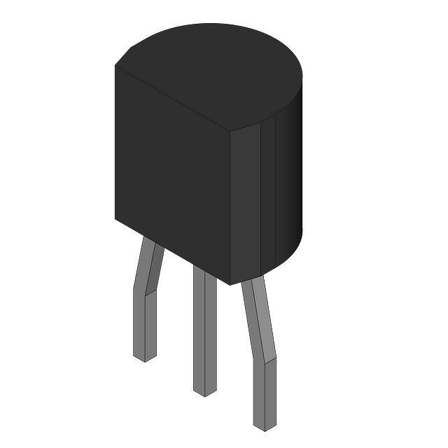
Figure 4. T-3 (TO-92)
The TMP37 is intended for applications over the range of 5°C
to 100°C and provides an output scale factor of 20 mV/°C. The
TMP37 provides a 500 mV output at 25°C. Operation extends
to 150°C with reduced accuracy for all devices when operating
from a 5 V supply.
The TMP35/TMP36/TMP37 are available in low cost 3-lead
TO-92, 8-lead SOIC_N, and 5-lead SOT-23 surface-mount
packages.
Document Feedback
Information furnished by Analog Devices is believed to be accurate and reliable. However, no
responsibility is assumed by Analog Devices for its use, nor for any infringements of patents or other
rights of third parties that may result from its use. Specifications subject to change without notice. No
license is granted by implication or otherwise under any patent or patent rights of Analog Devices.
Trademarks and registered trademarks are the property of their respective owners.
One Technology Way, P.O. Box 9106, Norwood, MA 02062-9106, U.S.A.
Tel: 781.329.4700 ©1996–2013 Analog Devices, Inc. All rights reserved.
Technical Support
www.analog.com
�TMP35/TMP36/TMP37
Data Sheet
TABLE OF CONTENTS
Features .............................................................................................. 1
Basic Temperature Sensor Connections.................................. 10
Applications ....................................................................................... 1
Fahrenheit Thermometers ........................................................ 10
General Description ......................................................................... 1
Average and Differential Temperature Measurement ........... 12
Functional Block Diagram .............................................................. 1
Microprocessor Interrupt Generator ....................................... 13
Pin Configurations ........................................................................... 1
Revision History ............................................................................... 2
Thermocouple Signal Conditioning with Cold-Junction
Compensation............................................................................. 14
Specifications..................................................................................... 3
Using TMP3x Sensors in Remote Locations .......................... 15
Absolute Maximum Ratings............................................................ 4
Temperature to 4–20 mA Loop Transmitter .......................... 15
Thermal Resistance ...................................................................... 4
Temperature-to-Frequency Converter .................................... 16
ESD Caution .................................................................................. 4
Driving Long Cables or Heavy Capacitive Loads .................. 17
Typical Performance Characteristics ............................................. 5
Commentary on Long-Term Stability ..................................... 17
Functional Description .................................................................... 8
Outline Dimensions ....................................................................... 18
Applications Information ................................................................ 9
Ordering Guide .......................................................................... 19
Shutdown Operation .................................................................... 9
Automotive Products ................................................................. 20
Mounting Considerations ........................................................... 9
Thermal Environment Effects .................................................... 9
REVISION HISTORY
11/13—Rev. F to Rev. G
10/02—Rev. B to Rev. C
Change to Table 1, Long-Term Stability Parameter ..................... 3
Change to Caption for Figure 38 .................................................. 18
Changes to Ordering Guide .......................................................... 19
11/10—Rev. E to Rev. F
Changes to Specifications .................................................................3
Deleted Text from Commentary on Long-Term Stability
Section.............................................................................................. 13
Updated Outline Dimensions ....................................................... 14
Changes to Features.......................................................................... 1
Updated Outline Dimensions ....................................................... 18
Changes to Ordering Guide .......................................................... 19
Added Automotive Products Section .......................................... 20
Edits to Specifications .......................................................................2
Addition of New Figure 1 .................................................................2
Deletion of Wafer Test Limits Section ............................................3
8/08—Rev. D to Rev. E
6/97—Rev. 0 to Rev. A
Updated Outline Dimensions ....................................................... 18
Changes to Ordering Guide .......................................................... 19
3/96—Revision 0: Initial Version
9/01—Rev. A to Rev. B
3/05—Rev. C to Rev. D
Updated Format .................................................................. Universal
Changes to Specifications ................................................................ 3
Additions to Absolute Maximum Ratings ..................................... 4
Updated Outline Dimensions ....................................................... 18
Changes to Ordering Guide .......................................................... 19
Rev. G | Page 2 of 20
�Data Sheet
TMP35/TMP36/TMP37
SPECIFICATIONS
VS = 2.7 V to 5.5 V, −40°C ≤ TA ≤ +125°C, unless otherwise noted.
Table 1.
Parameter 1
ACCURACY
TMP35/TMP36/TMP37 (F Grade)
TMP35/TMP36/TMP37 (G Grade)
TMP35/TMP36/TMP37 (F Grade)
TMP35/TMP36/TMP37 (G Grade)
Scale Factor, TMP35
Scale Factor, TMP36
Scale Factor, TMP37
Symbol
Load Regulation
Power Supply Rejection Ratio
Linearity
Long-Term Stability
SHUTDOWN
Logic High Input Voltage
Logic Low Input Voltage
OUTPUT
TMP35 Output Voltage
TMP36 Output Voltage
TMP37 Output Voltage
Output Voltage Range
Output Load Current
Short-Circuit Current
Capacitive Load Driving
Device Turn-On Time
POWER SUPPLY
Supply Range
Supply Current
Supply Current (Shutdown)
1
2
PSRR
Test Conditions/Comments
Min
TA = 25°C
TA = 25°C
Over rated temperature
Over rated temperature
10°C ≤ TA ≤ 125°C
−40°C ≤ TA ≤ +125°C
5°C ≤ TA ≤ 85°C
5°C ≤ TA ≤ 100°C
3.0 V ≤ VS ≤ 5.5 V
0 µA ≤ IL ≤ 50 µA
−40°C ≤ TA ≤ +105°C
−105°C ≤ TA ≤ +125°C
TA = 25°C
3.0 V ≤ VS ≤ 5.5 V
TA = 150°C for 1000 hours
VIH
VIL
VS = 2.7 V
VS = 5.5 V
VS
ISY (ON)
ISY (OFF)
Max
Unit
±1
±1
±2
±2
10
10
20
20
±2
±3
±3
±4
°C
°C
°C
°C
mV/°C
mV/°C
mV/°C
mV/°C
6
25
30
50
0.5
0.4
20
60
100
m°C/µA
m°C/µA
m°C/V
m°C/V
°C
°C
1.8
400
TA = 25°C
TA = 25°C
TA = 25°C
IL
ISC
CL
Typ
250
750
500
10000
0.5
1
mV
mV
mV
mV
µA
µA
pF
ms
0.01
5.5
50
0.5
V
µA
µA
100
0
Note 2
No oscillations 2
Output within ±1°C, 100 kΩ||100 pF load2
1000
2000
50
250
2.7
Unloaded
Unloaded
Does not consider errors caused by self-heating.
Guaranteed but not tested.
Rev. G | Page 3 of 20
V
mV
�TMP35/TMP36/TMP37
Data Sheet
ABSOLUTE MAXIMUM RATINGS
Table 2.
Parameter1, 2
Supply Voltage
Shutdown Pin
Output Pin
Operating Temperature Range
Die Junction Temperature
Storage Temperature Range
IR Reflow Soldering
Peak Temperature
Time at Peak Temperature Range
Ramp-Up Rate
Ramp-Down Rate
Time 25°C to Peak Temperature
IR Reflow Soldering—Pb-Free Package
Peak Temperature
Time at Peak Temperature Range
Ramp-Up Rate
Ramp-Down Rate
Time 25°C to Peak Temperature
Rating
7V
GND ≤ SHUTDOWN ≤ +VS
GND ≤ VOUT ≤ +VS
−55°C to +150°C
175°C
−65°C to +160°C
220°C (0°C/5°C)
10 sec to 20 sec
3°C/sec
−6°C/sec
6 min
260°C (0°C)
20 sec to 40 sec
3°C/sec
−6°C/sec
8 min
Stresses above those listed under Absolute Maximum Ratings
may cause permanent damage to the device. This is a stress
rating only; functional operation of the device at these or any
other conditions above those indicated in the operational
section of this specification is not implied. Exposure to absolute
maximum rating conditions for extended periods may affect
device reliability.
THERMAL RESISTANCE
θJA is specified for the worst-case conditions, that is, a device in
socket.
Table 3. Thermal Resistance
Package Type
TO-92 (T-3-1)
SOIC_N (R-8)
SOT-23 (RJ-5)
ESD CAUTION
Digital inputs are protected; however, permanent damage can occur on
unprotected units from high energy electrostatic fields. Keep units in
conductive foam or packaging at all times until ready to use. Use proper
antistatic handling procedures.
2
Remove power before inserting or removing units from their sockets.
1
Rev. G | Page 4 of 20
θJA
162
158
300
θJC
120
43
180
Unit
°C/W
°C/W
°C/W
�Data Sheet
TMP35/TMP36/TMP37
TYPICAL PERFORMANCE CHARACTERISTICS
0.4
30
20
10
0
50
TEMPERATURE (°C)
100
0.3
0.2
0.1
0
–50
150
Figure 5. Load Regulation vs. Temperature (m°C/µA)
1.2
1.0
0.8
a
0.6
00337-007
0.4
0.2
0
25
50
TEMPERATURE (°C)
75
100
POWER SUPPLY REJECTION (°C/V)
OUTPUT VOLTAGE (V)
b
–25
75
125
100
31.600
c
1.4
0
–50
25
50
TEMPERATURE (°C)
100.000
a. TMP35
b. TMP36
c. TMP37
+VS = 3V
1.6
0
Figure 8. Power Supply Rejection vs. Temperature
2.0
1.8
–25
10.000
3.160
1.000
0.320
0.100
0.032
00337-010
0
–50
+VS = 3V TO 5.5V, NO LOAD
00337-009
POWER SUPPLY REJECTION (°C/V)
40
00337-005
LOAD REGULATION (m°C/µA)
50
0.010
20
125
100
1k
FREQUENCY (Hz)
100k
10k
Figure 9. Power Supply Rejection vs. Frequency
Figure 6. Output Voltage vs. Temperature
5
5
4
MINIMUM SUPPLY VOLTAGE (V)
a. MAXIMUM LIMIT (G GRADE)
b. TYPICAL ACCURACY ERROR
c. MINIMUM LIMIT (G GRADE)
1
0
–1
b
–2
–3
–4
c
–5
0
20
40
60
80
100
TEMPERATURE (°C)
120
MINIMUM SUPPLY VOLTAGE REQUIRED TO MEET
DATA SHEET SPECIFICATION
4
NO LOAD
3
b
2
a
1
a. TMP35/TMP36
b. TMP37
0
–50
140
–25
0
25
50
TEMPERATURE (°C)
00337-011
a
2
00337-008
ACCURACY ERROR (°C)
3
75
100
Figure 10. Minimum Supply Voltage vs. Temperature
Figure 7. Accuracy Error vs. Temperature
Rev. G | Page 5 of 20
125
�TMP35/TMP36/TMP37
Data Sheet
60
400
a. +VS = 5V
b. +VS = 3V
300
NO LOAD
RESPONSE TIME (µs)
SUPPLY CURRENT (µA)
50
40
a
30
= +VS AND SHUTDOWN PINS
HIGH TO LOW (3V TO 0V)
200
= +VS AND SHUTDOWN PINS
LOW TO HIGH (0V TO 3V)
VOUT SETTLES WITHIN ±1°C
100
b
–25
0
25
50
TEMPERATURE (°C)
75
100
00337-015
10
–50
00337-012
20
0
–50
125
Figure 11. Supply Current vs. Temperature
–25
0
25
50
TEMPERATURE (°C)
75
100
125
Figure 14. VOUT Response Time for +VS Power-Up/Power-Down vs.
Temperature
400
50
= SHUTDOWN PIN
HIGH TO LOW (3V TO 0V)
TA = 25°C, NO LOAD
300
30
20
200
100
= SHUTDOWN PIN
LOW TO HIGH (0V TO 3V)
VOUT SETTLES WITHIN ±1°C
00337-013
10
0
1
5
3
4
SUPPLY VOLTAGE (V)
2
6
0
–50
8
7
75
100
125
0.8
a. +VS = 5V
b. +VS = 3V
TA = 25°C
+VS = 3V
SHUTDOWN =
SIGNAL
0.6
OUTPUT VOLTAGE (V)
NO LOAD
30
20
a
10
0.4
0.2
0
1.0
0.8
0.6
TA = 25°C
+VS AND SHUTDOWN =
SIGNAL
0.4
00337-014
SUPPLY CURRENT (nA)
25
50
TEMPERATURE (°C)
1.0
50
b
0
–50
0
Figure 15. VOUT Response Time for SHUTDOWN Pin vs. Temperature
Figure 12. Supply Current vs. Supply Voltage
40
–25
–25
0
25
50
TEMPERATURE (°C)
75
100
0.2
0
–50
125
Figure 13. Supply Current vs. Temperature (Shutdown = 0 V)
00337-017
0
00337-016
RESPONSE TIME (µs)
SUPPLY CURRENT (µA)
40
0
50
100
150 200 250
TIME (µs)
300
350
400
450
Figure 16. VOUT Response Time to SHUTDOWN Pin and +VS Pin vs. Time
Rev. G | Page 6 of 20
�Data Sheet
TMP35/TMP36/TMP37
110
a
10mV
100
90
90
VOLT/DIVISION
70
60
50
40
a. TMP35 SOIC SOLDERED TO 0.5" × 0.3" Cu PCB
b. TMP36 SOIC SOLDERED TO 0.6" × 0.4" Cu PCB
c. TMP35 TO-92 IN SOCKET SOLDERED TO
1" × 0.4" Cu PCB
00337-034
20
10
0%
00337-019
30
10
0
100
0
200
300
TIME (s)
400
500
TIME/DIVISION
600
Figure 17. Thermal Response Time in Still Air
Figure 20. Temperature Sensor Wideband Output Noise Voltage;
Gain = 100, BW = 157 kHz
140
2400
a. TMP35 SOIC SOLDERED TO 0.5" × 0.3" Cu PCB
b. TMP36 SOIC SOLDERED TO 0.6" × 0.4" Cu PCB
c. TMP35 TO-92 IN SOCKET SOLDERED TO
1" × 0.4" Cu PCB
2200
VOLTAGE NOISE DENSITY (nV/ Hz)
TIME CONSTANT (s)
120
100
80
+VS = 3V, 5V
60
b
40
c
00337-018
20
a
0
0
100
200
300
400
500
AIR VELOCITY (FPM)
600
60
50
40
a. TMP35 SOIC SOLDERED TO 0.5" × 0.3" Cu PCB
b. TMP36 SOIC SOLDERED TO 0.6" × 0.4" Cu PCB
c. TMP35 TO-92 IN SOCKET SOLDERED TO
1" × 0.4" Cu PCB
20
00337-035
CHANGE (%)
+VS = 3V, 5V
b
30
10
0
0
10
20
30
TIME (s)
40
50
1200
1000
800
600
a
400
a. TMP35/TMP36
b. TMP37
100
1k
FREQUENCY (Hz)
Figure 21. Voltage Noise Spectral Density vs. Frequency
90
70
1400
10
a
c
1600
0
700
100
80
b
1800
200
Figure 18. Thermal Response Time Constant in Forced Air
110
2000
00337-020
CHANGE (%)
100
+VS = 3V, 5V
c
b
80
1ms
60
Figure 19. Thermal Response Time in Stirred Oil Bath
Rev. G | Page 7 of 20
10k
�TMP35/TMP36/TMP37
Data Sheet
FUNCTIONAL DESCRIPTION
An equivalent circuit for the TMP3x family of micropower,
centigrade temperature sensors is shown in Figure 22. The core
of the temperature sensor is a band gap core that comprises
transistors Q1 and Q2, biased by Q3 to approximately 8 µA. The
band gap core operates both Q1 and Q2 at the same collector
current level; however, because the emitter area of Q1 is 10
times that of Q2, the VBE of Q1 and the VBE of Q2 are not equal
by the following relationship:
+VS
SHUTDOWN
25µA
3X
Q2
1X
Q4
AE,Q1
∆VBE = VT × ln
AE,Q2
2X
R1
Q1
10X
R3
Resistors R1 and R2 are used to scale this result to produce
the output voltage transfer characteristic of each temperature
sensor and, simultaneously, R2 and R3 are used to scale the VBE of
Q1 as an offset term in VOUT. Table 4 summarizes the differences
in the output characteristics of the three temperature sensors.
The output voltage of the temperature sensor is available at the
emitter of Q4, which buffers the band gap core and provides
load current drive. The current gain of Q4, working with the
available base current drive from the previous stage, sets the
short-circuit current limit of these devices to 250 µA.
R2
VOUT
7.5µA
2X
6X
GND
00337-006
Q3
Figure 22. Temperature Sensor Simplified Equivalent Circuit
Table 4. TMP3x Output Characteristics
Sensor
TMP35
TMP36
TMP37
Rev. G | Page 8 of 20
Offset
Voltage (V)
0
0.5
0
Output Voltage
Scaling (mV/°C)
10
10
20
Output Voltage
at 25°C (mV)
250
750
500
�Data Sheet
TMP35/TMP36/TMP37
APPLICATIONS INFORMATION
SHUTDOWN OPERATION
THERMAL ENVIRONMENT EFFECTS
All TMP3x devices include a shutdown capability, which
reduces the power supply drain to less than 0.5 µA maximum.
This feature, available only in the SOIC_N and the SOT-23
packages, is TTL/CMOS level-compatible, provided that the
temperature sensor supply voltage is equal in magnitude to the
logic supply voltage. Internal to the TMP3x at the SHUTDOWN
pin, a pull-up current source to +VS is connected. This allows
the SHUTDOWN pin to be driven from an open-collector/drain
driver. A logic low, or zero-volt condition, on the SHUTDOWN
pin is required to turn off the output stage. During shutdown,
the output of the temperature sensors becomes high impedance
where the potential of the output pin is then determined by
external circuitry. If the shutdown feature is not used, it is
recommended that the SHUTDOWN pin be connected to +VS
(Pin 8 on the SOIC_N; Pin 2 on the SOT-23).
The thermal environment in which the TMP3x sensors are used
determines two important characteristics: self-heating effects
and thermal response time. Figure 23 illustrates a thermal model
of the TMP3x temperature sensors, which is useful in understanding these characteristics.
The shutdown response time of these temperature sensors is
shown in Figure 14, Figure 15, and Figure 16.
MOUNTING CONSIDERATIONS
If the TMP3x temperature sensors are thermally attached and
protected, they can be used in any temperature measurement
application where the maximum temperature range of the
medium is between −40°C and +125°C. Properly cemented or
glued to the surface of the medium, these sensors are within
0.01°C of the surface temperature. Caution should be exercised,
especially with T-3 packages, because the leads and any wiring
to the device can act as heat pipes, introducing errors if the
surrounding air-surface interface is not isothermal. Avoiding this
condition is easily achieved by dabbing the leads of the temperature sensor and the hookup wires with a bead of thermally
conductive epoxy. This ensures that the TMP3x die temperature
is not affected by the surrounding air temperature. Because
plastic IC packaging technology is used, excessive mechanical
stress should be avoided when fastening the device with a clamp
or a screw-on heat tab. Thermally conductive epoxy or glue,
which must be electrically nonconductive, is recommended
under typical mounting conditions.
These temperature sensors, as well as any associated circuitry,
should be kept insulated and dry to avoid leakage and corrosion.
In wet or corrosive environments, any electrically isolated metal
or ceramic well can be used to shield the temperature sensors.
Condensation at very cold temperatures can cause errors and
should be avoided by sealing the device, using electrically nonconductive epoxy paints or dip or any one of the many printed
circuit board coatings and varnishes.
TJ
CCH
TC
CC
θCA
TA
00337-021
PD
θJC
Figure 23. Thermal Circuit Model
In the T-3 package, the thermal resistance junction-to-case, θJC,
is 120°C/W. The thermal resistance case-to-ambient, CA, is the
difference between θJA and θJC, and is determined by the characteristics of the thermal connection. The power dissipation of
the temperature sensor, PD, is the product of the total voltage
across the device and its total supply current, including any
current delivered to the load. The rise in die temperature above
the ambient temperature of the medium is given by
TJ = PD × (θJC + θCA) + TA
Thus, the die temperature rise of a TMP35 SOT-23 package
mounted into a socket in still air at 25°C and driven from a 5 V
supply is less than 0.04°C.
The transient response of the TMP3x sensors to a step change
in the temperature is determined by the thermal resistances and
the thermal capacities of the die, CCH, and the case, CC. The
thermal capacity of CC varies with the measurement medium
because it includes anything in direct contact with the package.
In all practical cases, the thermal capacity of CC is the limiting
factor in the thermal response time of the sensor and can be
represented by a single-pole RC time constant response. Figure 17
and Figure 19 show the thermal response time of the TMP3x
sensors under various conditions. The thermal time constant
of a temperature sensor is defined as the time required for the
sensor to reach 63.2% of the final value for a step change in the
temperature. For example, the thermal time constant of a
TMP35 SOIC package sensor mounted onto a 0.5" × 0.3" PCB is
less than 50 sec in air, whereas in a stirred oil bath, the time
constant is less than 3 sec.
Rev. G | Page 9 of 20
�TMP35/TMP36/TMP37
Data Sheet
BASIC TEMPERATURE SENSOR CONNECTIONS
FAHRENHEIT THERMOMETERS
Figure 24 illustrates the basic circuit configuration for the
TMP3x family of temperature sensors. The table in Figure 24
shows the pin assignments of the temperature sensors for the
three package types. For the SOT-23, Pin 3 is labeled NC, as are
Pin 2, Pin 3, Pin 6, and Pin 7 on the SOIC_N package. It is
recommended that no electrical connections be made to these
pins. If the shutdown feature is not needed on the SOT-23 or
on the SOIC_N package, the SHUTDOWN pin should be
connected to +VS.
Although the TMP3x temperature sensors are centigrade
temperature sensors, a few components can be used to convert
the output voltage and transfer characteristics to directly read
Fahrenheit temperatures. Figure 25 shows an example of a
simple Fahrenheit thermometer using either the TMP35 or the
TMP37. Using the TMP35, this circuit can be used to sense
temperatures from 41°F to 257°F with an output transfer
characteristic of 1 mV/°F; using the TMP37, this circuit can be
used to sense temperatures from 41°F to 212°F with an output
transfer characteristic of 2 mV/°F. This particular approach
does not lend itself to the TMP36 because of its inherent 0.5 V
output offset. The circuit is constructed with an AD589, a 1.23 V
voltage reference, and four resistors whose values for each sensor
are shown in the table in Figure 25. The scaling of the output
resistance levels ensures minimum output loading on the temperature sensors. A generalized expression for the transfer
equation of the circuit is given by
2.7V < +VS < 5.5V
0.1µF
+VS
VOUT
GND
R1
(TMP35 ) + R3 ( AD589 )
VOUT =
R3 + R4
R1 + R2
+VS
GND
VOUT
SHUTDOWN
SOIC_N
8
4
1
5
SOT-23
TO-92
2
1
5
3
1
2
4
NA
PACKAGE
00337-022
PIN ASSIGNMENTS
Figure 24. Basic Temperature Sensor Circuit Configuration
Note the 0.1 µF bypass capacitor on the input. This capacitor
should be a ceramic type, have very short leads (surface-mount
is preferable), and be located as close as possible in physical
proximity to the temperature sensor supply pin. Because these
temperature sensors operate on very little supply current and
may be exposed to very hostile electrical environments, it is
important to minimize the effects of radio frequency interference
(RFI) on these devices. The effect of RFI on these temperature
sensors specifically and on analog ICs in general is manifested as
abnormal dc shifts in the output voltage due to the rectification
of the high frequency ambient noise by the IC. When the
devices are operated in the presence of high frequency radiated
or conducted noise, a large value tantalum capacitor (±2.2 µF)
placed across the 0.1 µF ceramic capacitor may offer additional
noise immunity.
where:
TMP35 is the output voltage of the TMP35 or the TMP37 at the
measurement temperature, TM.
AD589 is the output voltage of the reference, that is, 1.23 V.
The output voltage of this circuit is not referenced to the
circuit’s common ground. If this output voltage were applied
directly to the input of an ADC, the ADC common ground
should be adjusted accordingly.
+VS
0.1µF
+VS
TMP35/
TMP37
VOUT
R1
GND
+
R2
VOUT
AD589
1.23V
R3
–
R4
SENSOR
TCVOUT R1 (kΩ) R2 (kΩ) R3 (kΩ) R4 (kΩ)
TMP35
TMP37
1mV/°F
2mV/°F
45.3
45.3
10
10
10
10
374
182
Figure 25. TMP35/TMP37 Fahrenheit Thermometers
Rev. G | Page 10 of 20
00337-023
TMP3x
SHUTDOWN
�Data Sheet
TMP35/TMP36/TMP37
The same circuit principles can be applied to the TMP36, but
because of the inherent offset of the TMP36, the circuit uses only
two resistors, as shown in Figure 26. In this circuit, the output
voltage transfer characteristic is 1 mV/°F but is referenced to
the common ground of the circuit; however, there is a 58 mV
(58°F) offset in the output voltage. For example, the output
voltage of the circuit reads 18 mV if the TMP36 is placed in a
−40°F ambient environment and 315 mV at +257°F.
At the expense of additional circuitry, the offset produced by
the circuit in Figure 26 can be avoided by using the circuit in
Figure 27. In this circuit, the output of the TMP36 is conditioned
by a single-supply, micropower op amp, the OP193. Although
the entire circuit operates from a single 3 V supply, the output
voltage of the circuit reads the temperature directly, with a
transfer characteristic of 1 mV/°F, without offset. This is accomplished through an ADM660, which is a supply voltage inverter.
The 3 V supply is inverted and applied to the V− terminal of the
OP193. Thus, for a temperature range between −40°F and +257°F,
the output of the circuit reads −40 mV to +257 mV. A general
expression for the transfer equation of the circuit is given by
+VS
+VS
VOUT
R6
1 + R4 (TMP36 ) − R4 VS
VOUT =
R5 + R6
R3
R3 2
R1
45.3kΩ
GND
R2
10kΩ
VOUT @ 1mV/°F – 58°F
00337-024
TMP36
0.1µF
VOUT @ –40°F = 18mV
VOUT @ +257°F = 315mV
Figure 26. TMP36 Fahrenheit Thermometer Version 1
+3V
R1
50kΩ
R3
R4
C1 +
10µF
R2
50kΩ
0.1µF
7
2
+VS
10µF/0.1µF
VOUT
TMP36
OP193
R5
3
6
VOUT @ 1mV/°F
–40°F ≤ TA ≤ +257°F
+
4
R6
GND
8
1
5
NC
ELEMENT
VALUE
R3
258.6kΩ
R4
10kΩ
R5
47.7kΩ
R6
10kΩ
–3V
2
ADM660
+
10µF
6
+
10µF
4
3
NC
7
00337-025
+
–
Figure 27. TMP36 Fahrenheit Thermometer Version 2
Rev. G | Page 11 of 20
�TMP35/TMP36/TMP37
Data Sheet
AVERAGE AND DIFFERENTIAL TEMPERATURE
MEASUREMENT
2.7V < +VS < 5.5V
0.1µF
In Figure 28, an OP193 sums the outputs of three temperature
sensors to produce an output voltage scaled by 10 mV/°C that
represents the average temperature at three locations. The circuit
can be extended to include as many temperature sensors as
required as long as the transfer equation of the circuit is
maintained. In this application, it is recommended that one
temperature sensor type be used throughout the circuit;
otherwise, the output voltage of the circuit cannot produce an
accurate reading of the various ambient conditions.
The circuit in Figure 29 illustrates how a pair of TMP3x sensors
used with an OP193 configured as a difference amplifier can
read the difference in temperature between two locations. In
these applications, it is always possible that one temperature
sensor is reading a temperature below that of the other sensor.
To accommodate this condition, the output of the OP193 is
offset to a voltage at one-half the supply via R5 and R6. Thus,
the output voltage of the circuit is measured relative to this
point, as shown in Figure 29. Using the TMP36, the output
voltage of the circuit is scaled by 10 mV/°C. To minimize the
error in the difference between the two measured temperatures,
a common, readily available thin-film resistor network is used
for R1 to R4.
2
3
TMP3x
VTEMP(AVG)
@ 10mV/°C FOR TMP35/TMP36
@ 20mV/°C FOR TMP37
7
–
6
OP193
+
4
R5
100kΩ
R1
300kΩ
R6
7.5kΩ
R2
300kΩ
TMP3x
FOR R1 = R2 = R3 = R;
TMP3x
R3
300kΩ
R4
7.5kΩ
VTEMP(AVG) = 1 (TMP3x1 + TMP3x2 + TMP3x3)
3
R5 = R1
3
R4 = R6
00337-026
In many commercial and industrial environments, temperature
sensors often measure the average temperature in a building, or
the difference in temperature between two locations on a factory
floor or in an industrial process. The circuits in Figure 28 and
Figure 29 demonstrate an inexpensive approach to average and
differential temperature measurement.
Figure 28. Configuring Multiple Sensors for
Average Temperature Measurements
2.7V < +VS < 5.5V
0.1µF
TMP36
@ T1
R11
R21
R8
25kΩ
0.1µF
7
2
0.1µF
TMP36
R31
–
OP193
3
@ T2
6
VOUT
+
4
R7
100kΩ
R9
25kΩ
CENTERED AT
0°C ≤ TA ≤ 125°C
R5
100kΩ
1µF
R6
100kΩ
VOUT = T2 – T1 @ 10mV/°C
VS
CENTERED AT
2
NOTE:
1 R1–R4, CADDOCK T914–100k–100, OR EQUIVALENT.
Figure 29. Configuring Multiple Sensors for
Differential Temperature Measurements
Rev. G | Page 12 of 20
00337-027
R41
�Data Sheet
TMP35/TMP36/TMP37
Because temperature is a slowly moving quantity, the possibility
for comparator chatter exists. To avoid this condition, hysteresis
is used around the comparator. In this application, a hysteresis
of 5°C about the trip point was arbitrarily chosen; the ultimate
value for hysteresis should be determined by the end application.
The output logic voltage swing of the comparator with R1 and
R2 determines the amount of comparator hysteresis. Using a
3.3 V supply, the output logic voltage swing of the CMP402 is
2.6 V; therefore, for a hysteresis of 5°C (50 mV at 10 mV/°C),
R1 is set to 20 kΩ, and R2 is set to 1 MΩ. An expression for the
hysteresis of this circuit is given by
MICROPROCESSOR INTERRUPT GENERATOR
These inexpensive temperature sensors can be used with a
voltage reference and an analog comparator to configure an
interrupt generator for microprocessor applications. With the
popularity of fast microprocessors, the need to indicate a
microprocessor overtemperature condition has grown
tremendously. The circuit in Figure 30 demonstrates one way to
generate an interrupt using a TMP35, a CMP402 analog
comparator, and a REF191, a 2 V precision voltage reference.
The circuit is designed to produce a logic high interrupt signal
if the microprocessor temperature exceeds 80°C. This 80°C trip
point was arbitrarily chosen (final value set by the microprocessor
thermal reference design) and is set using an R3 to R4 voltage
divider of the REF191 output voltage. Because the output of the
TMP35 is scaled by 10 mV/°C, the voltage at the inverting
terminal of the CMP402 is set to 0.8 V.
(
R1
VHYS =
VLOGIC SWING, CMP402
R2
)
Because this circuit is probably used in close proximity to high
speed digital circuits, R1 is split into equal values and a 1000 pF
capacitor is used to form a low-pass filter on the output of the
TMP35. Furthermore, to prevent high frequency noise from
contaminating the comparator trip point, a 0.1 µF capacitor is
used across R4.
3.3V
R2
1MΩ
+VS
TMP35
VOUT
6
4
–
CMP402
CL
1000pF
R5
100kΩ
GND
3
R1B
10kΩ
5
2
INTERRUPT
14
+
0.1µF
13
2
3
REF191
R3
16kΩ
6
+
4
C1 =
1µF
>80°C


 工商网监
湘ICP备2023018690号
工商网监
湘ICP备2023018690号
