[AK5522]
AK5522
Differential Input Stereo 32-bit ADC with Excellent PSRR
1. General Description
The AK5522 is a 32-bit, from 8kHz to 192kHz sampling A/D converter for line and microphone inputs of
digital audio systems. It achieves 108dB dynamic range and 98dB S/(N+D) while keeping low power
consumption performance. Four types of digital filters are integrated and selectable according to the
sound quality preference.
The AK5522 has great power supply rejection ratio, (PSRR), and common mode rejection ratio, (CMRR),
enabling to maintain sufficient characteristics when connecting USB bus power or DCDC converter
output as a power supply. It is suitable for applications with noisy power supply such as USB audio
interface, wireless speakers and car audio equipment.
In addition, the AK5522 integrates a regulator with high PSRR for DAC power supply. Using the AK5522
with a DAC such as the AK4432 or the AK4452, it is enable to bring maximum DAC performance even in
a poor power supply condition. Moreover, the AK5522 integrates low-jitter PLL circuit that generates a
master clock for DAC from LRCK or BICK. It provides a low-EMI solution by avoiding unnecessary
drawing of the master clock that has high frequency, on the board.
The AK5522 helps reducing components and a mounting space with these features for environmental
noise.
2. Features
Sampling Rate:
8kHz - 192kHz
Input:
Full Differntial, Pseudo Differential, Single-Ended
S/(N+D):
98dB typ.
DR, S/N:
108dB typ.
PSRR:
80dB typ.
CMRR:
80dB typ.
Internal Filter:
Four types of LPF, Digital HPF
Short Group Delay:
4.4/fs (Short Delay Slow roll-off)
Output Format:
32-bit MSB justified, I2S or TDM (Cascade Connection available)
Operation Mode:
Master or Slave Modes
Programmable Gain Amp: 3dB - +12dB/1dB (Fixed at 0dB in Parallel Control mode)
Integrated PLL:
Generates the master clock from BICK or LRCK
Master Clock Output:
Output master clock generated by the PLL
Voltage Regulator for External DAC Power: Generates 3.3V from 5V applied to AVDD pin.
Power Supply:
Analog 4.5 - 5.5V or 3.0 - 3.6V, Digital 3.0 - 3.6V or 1.7 - 1.98V
Control Mode:
Parallel Control mode (Pin setting)
Serial Control mode (I2C Bus setting)
Power Consumption:
76 mW (@AVDD=5.0V, DVDD=3.3V, fs=48kHz)
Operation Temperature:
40 - 105C
Package:
24-pin QFN 4mmx4mm, 0.5mm pitch
017002311-E-00
2017/03
-1-
�[AK5522]
3. Table of Contents
General Description ............................................................................................................................ 1
Features .............................................................................................................................................. 1
Table of Contents................................................................................................................................ 2
Block Diagram..................................................................................................................................... 4
■ Block Diagram.................................................................................................................................... 4
5. Pin Configurations and Functions ...................................................................................................... 4
■ Pin Configurations ............................................................................................................................. 4
■ Pin Functions ..................................................................................................................................... 5
■ Handling of Unused Pin ..................................................................................................................... 6
6. Absolute Maximum Ratings ................................................................................................................ 7
7. Recommended Operation Conditions ................................................................................................ 7
8. Analog Characteristics ........................................................................................................................ 8
■ Analog Power Supply=5.0V ............................................................................................................... 8
■ Analog Power Supply=3.3V ............................................................................................................... 9
9. Filter Characteristics ......................................................................................................................... 10
■ ADC Filter Characteristics (fs= 48kHz) ........................................................................................... 10
■ ADC Filter Characteristics (fs= 96kHz) ........................................................................................... 12
■ ADC Filter Characteristics (fs= 192kHz) ......................................................................................... 14
10.
DC Characteristics ........................................................................................................................ 16
11.
Switching Characteristics (Parallel Control Mode) ....................................................................... 17
■ System Clocks ................................................................................................................................. 17
■ Audio Interface ................................................................................................................................. 21
■ Power-down, Reset (Parallel Control Mode) ................................................................................... 22
■ Timing Diagram (Parallel Control Mode) ......................................................................................... 22
12.
Switching Characteristics (Serial Control Mode) .......................................................................... 25
■ System Clocks ................................................................................................................................. 25
■ Audio Interface ................................................................................................................................. 32
■ I2C Bus, Power-down, Reset (Serial Control Mode) ....................................................................... 34
■ Timing Diagram (Serial Control Mode) ............................................................................................ 35
13.
Functional Descriptions (Parallel Control Mode) .......................................................................... 40
■ Digital Power Supply........................................................................................................................ 40
■ Analog Power Supply ...................................................................................................................... 40
■ Regulator for External DAC Power Supply ..................................................................................... 40
■ Parallel / Serial Control Mode .......................................................................................................... 40
■ System Clocks (Parallel Control Mode) .......................................................................................... 40
■ Operation Mode (Parallel Control Mode)......................................................................................... 42
■ Audio Interface Format (Parallel Control Mode) ............................................................................. 46
■ Cascade Connection in TDM Mode (Parallel Control Mode) .......................................................... 46
■ Digital HPF (Parallel Control Mode) ................................................................................................ 49
■ Digital Filter Setting (Parallel Control Mode) ................................................................................... 49
■ Input Gain (Parallel Control Mode) .................................................................................................. 49
■ Power-up Function/ Sequence (Parallel Control Mode) ................................................................. 49
■ Power Down Function/ Sequence ................................................................................................... 52
14.
Functional Descriptions (Serial Control Mode) ............................................................................. 53
■ Digital Power Supply........................................................................................................................ 53
■ Analog Power Supply ...................................................................................................................... 53
■ Regulator for External DAC Power Supply ..................................................................................... 53
■ Parallel / Serial Control Mode .......................................................................................................... 53
■ System Clocks (Serial Control Mode) ............................................................................................. 53
■ Audio Interface Format (Serial Control Mode) ................................................................................ 62
■ Cascade Connection in TDM Mode (Serial Control Mode)............................................................. 62
1.
2.
3.
4.
017002311-E-00
2017/03
-2-
�[AK5522]
■ Digital HPF (Serial Control Mode) ................................................................................................... 66
■ Digital Filter Setting (Serial Control Mode) ...................................................................................... 66
■ Input Gain (Serial Control Mode) ..................................................................................................... 67
■ Device Reset (Serial Control Mode) ................................................................................................ 67
■ Block Power Control (Serial Control Mode) .................................................................................... 67
■ Power up Function/ Sequence (Serial Control Mode)..................................................................... 67
■ Power Down Function/ Sequence ................................................................................................... 72
■ Register Control Interface ................................................................................................................ 72
■ Register Map .................................................................................................................................... 76
■ Register Definitions.......................................................................................................................... 76
15.
Recommended External Circuits .................................................................................................. 78
16.
Package......................................................................................................................................... 82
■ Outline Dimensions .......................................................................................................................... 82
■ Material & Lead Finish ..................................................................................................................... 82
■ Marking ............................................................................................................................................ 82
17.
Ordering Guide .............................................................................................................................. 83
■ Ordering Guide ................................................................................................................................ 83
18.
Revision History ............................................................................................................................ 83
IMPORTANT NOTICE ........................................................................................................................... 84
017002311-E-00
2017/03
-3-
�[AK5522]
4. Block Diagram
■ Block Diagram
AVDD
VREF
REGAO
LINP
LINN
REGDO
DVSS
LOOP
3.3V
Regulator
(for DAC)
5V or 3.3V
AVSS
DVDD
Regulator
(Digital)
3.3V or 1.8V
PLL
1.8V
3dB ~ 12dB/ 1dB step
+
-
AAF
Delta-Sigma
Modulator
Decimation
Filter
AAF
Delta-Sigma
Modulator
Decimation
Filter
MCLK
1fs
64fs
HPF
Serial
Output
Interface
BICK
LRCK
SDTO
CKS3/SDA
RINP
RINN
+
-
CKS2/SCL
HPF
CKS1
CKS0/TDMI
3dB ~ 12dB/ 1dB step
PDN
SD
DIF
PSN
Figure 1. Block Diagram
5. Pin Configurations and Functions
18
17
16
15
14
13
MCLK
DVDD
DVSS
REGAO
AVDD
AVSS
■ Pin Configurations
19
20
21
22
23
24
24QFN
TOP VIEW
12
11
10
9
8
7
LOOP
VREF
RINP
RINN
LINN
LINP
CKS3/SDA
PDN
CKS1
SD
PSN
DIF
1
2
3
4
5
6
REGDO
LRCK
BICK
SDTO
CKS0/TDMI
CKS2/SCL
Figure 2. Pin Configurations
017002311-E-00
2017/03
-4-
�[AK5522]
■ Pin Functions
No. Pin Name I/O
1
2
3
CKS3
SDA
PDN
CKS1
I
IO
I
I
4
SD
I
5
PSN
I
6
DIF
I
7
8
9
10
LINP
LINN
RINN
RINP
I
I
I
I
11 VREF
O
12 LOOP
O
13 AVSS
14 AVDD
P
P
15 REGAO
O
16 DVSS
17 DVDD
P
P
18 MCLK
I
O
19 REGDO
O
I
20 LRCK
I
O
21 BICK
I
O
22 SDTO
23 CKS0
TDMI
24 CKS2
SCL
O
I
I
I
I
Function
Clock Mode Select Pin in Parallel Control mode
2
Control Data I/O Pin for I C Bus in Serial Control mode
Reset and Power Down Pin
Clock Mode Select Pin
Digital Filter Select Pin in Parallel Control mode
“L”: Sharp Roll-Off, “H”: Short Delay Sharp Roll-Off
Control Mode Select Pin
“L”: Serial Control mode, “H”: Parallel Control mode
Data Format Select Pin in Parallel Control mode
2
“L”: MSB Justified, “H”: I S Compatible
L Channel Positive Signal Input Pin
L Channel Negative Signal Input Pin
R Channel Negative Signal Input Pin
R Channel Positive Signal Input Pin
Internal Reference Voltage Decoupling Pin
Decouple this pin to AVSS with a 1F50% capacitor.
PLL Loop Filter Connect Pin
Connect this pin to AVSS with a 0.01F50% capacitor.
Analog Ground Pin
Analog Power Supply Pin. 3.0 - 3.6V or 4.5 - 5.5V
Regulator for External DAC Output Pin
AVDD=4.5V - 5.5V: 3.3V typ.
AVDD=3.0V - 3.6V: Low (External capacitor is not necessary)
Connect to AVSS with a 10F50% capacitor. Additionally, this pin
must be decoupled to the power supply pin of an external DAC with a
10F50% and a 0.1F50% capacitors in parallel. (Figure 81,
Figure 82)
Digital Ground Pin
Digital Power Supply Pin. 3.0 - 3.6V
Master Clock Input Pin in EXT Master / EXT Slave / PLL Master mode
This pin is pulled-down to DVSS internally with a 100k resister.
Master Clock Output Pin in PLL Slave mode
This pin is pulled-down to DVSS internally with a 100k resister.
Regulator Stabilization Capacitor Connect Pin
DVDD=3.0V - 3.6V: Output 1.8V typ.
Connect to DVSS with a 1F50% capacitor.
DVDD=1.7V - 1.98V: Connect to DVDD
Channel Clock Input Pin in Slave mode
This pin is pulled-down to DVSS internally with a 100k resister.
Channel Clock Output Pin in Master mode
This pin is pulled-down to DVSS internally with a 100k resister.
Audio Serial Data Clock Input Pin in Slave mode
This pin is pulled-down to DVSS internally with a 100k resister.
Audio Serial Data Clock Output Pin in Master mode
This pin is pulled-down to DVSS internally with a 100k resister.
Audio Serial Data Output Pin
Clock Mode Select Pin in Parallel Control mode
TDM Data Input Pin in TDM mode
Clock Mode Select Pin in Parallel Control mode
2
Control Clock Input Pin for I C Bus in Serial Control mode
Power Down
Status
Hi-Z
Hi-Z
Hi-Z
Hi-Z
Hi-Z
Hi-Z
Hi-Z
Hi-Z
Hi-Z
Hi-Z
Hi-Z
Hi-Z,
Pulled-down
with 0.7k
Hi-Z
Hi-Z,
Pulled-down
with 0.5k
Hi-Z
(Input mode)
Hi-Z
Hi-Z
(Input mode)
Hi-Z
(Input mode)
L
Hi-Z
Hi-Z
Hi-Z
Hi-Z
I/O
I: Input, O: Output, IO: Input and Output, P: Power Supply
Note 1. All digital input pins must not be allowed to float.
017002311-E-00
2017/03
-5-
�[AK5522]
■ Handling of Unused Pin
The unused I/O pins should be connected appropriately.
Classification
Analog
Digital
Pin Name
LINP, LINN, RINP, RINN
REGAO
(AVDD = 4.5V - 5.5V, Regulator for DAC = Enable)
REGAO
(AVDD = 4.5V - 5.5V, Regulator for DAC = Disable)
REGAO (AVDD = 3.0V - 3.6V)
LOOP
CKS1, CKS0, SD, DIF (Serial Control mode)
TDMI (TDM mode)
MCLK (PLL Slave mode)
017002311-E-00
Setting
Open
Decouple with a 10 F capacitor
to AVSS
Open
Open
Open
Connect to DVSS
Connect to DVSS
Open
2017/03
-6-
�[AK5522]
6. Absolute Maximum Ratings
(AVSS=DVSS=0V; Note 2)
Parameter
Symbol
Min.
Analog (AVDD pin)
VA
−0.3
Power
Digital (DVDD pin)
VD
−0.3
Supplies
Digital (REGDO pin)
VRD
−0.3
Input Current (Any Pin Except Supplies)
IIN
Analog Input Voltage (LINP/N, RINP/N pins)
VINA
VDM−0.3
(Note 3)
Digital Input Voltage (Note 5)
VIND
−0.3
Max.
6.0
6.0
2.5
10
VDP+0.3 or 6.0
(Note 4)
VD+0.3 or 6.0
(Note 6)
105
150
Unit
V
V
V
mA
V
V
Ambient Temperature (Power applied)
Ta
−40
C
Storage Temperature
Tstg
−65
C
Note 2. All voltages with respect to ground.
Note 3. VDM and VDP are the voltages generated internally.
Note 4. The maximum value of input voltage is lower value between (VDP+0.3) V or 6.0 V.
Note 5. PDN, SD, LRCK, BICK, MCLK, PSN, CKS0/TDMI, CKS1, CKS2/SCL, CKS3/SDA and DIF pins
Note 6. The maximum value of input voltage is lower value between (VD+0.3) V or 6.0 V.
Mode
Power-down
Normal operation
AVDD
VDM
3.0 - 3.6V, 4.5 - 5.5V
AVSS
4.5 - 5.5V
−0.75V
3.0 - 3.6V
−1.50V
Table 1. VDM, VDP Voltage
VDP
AVDD
5.25V
4.50V
WARNING: Operation at or beyond these limits may result in permanent damage to the device.
Normal operation is not guaranteed at these extremes.
7. Recommended Operation Conditions
(AVSS=DVSS=0V; Note 2)
Parameter
Symbol
Min.
Typ.
Max. Unit
Analog (AVDD)
VA
4.5
5.0
5.5
V
Analog (AVDD)
VA
3.0
3.3
3.6
V
Power
Using internal regulator
Supplies
Digital (DVDD)
VD
3.0
3.3
3.6
V
Not using internal regulator
Digital (DVDD)
VD
1.7
1.8
1.98
V
Digital (REGDO)
VRD
Note 2. All voltages with respect to ground.
Note 7. The power up sequence between AVDD and DVDD is not critical. If DVDD is 1.7V to 1.98V then
the DVDD pin should be connect to the REGDO pin.
* AKM assumes no responsibility for the usage beyond the conditions in this data sheet.
017002311-E-00
2017/03
-7-
�[AK5522]
8. Analog Characteristics
■ Analog Power Supply=5.0V
(Ta=25C; AVDD=5.0V; DVDD=3.3V, fs=48kHz, 96kHz; 192kHz, BICK=64fs; Signal Frequency=1kHz;
32-bit Data; Measurement frequency=20Hz - 20kHz at fs=48kHz, 40Hz - 40kHz at fs=96kHz and
192kHz, Gain=0dB, unless otherwise specified.)
Parameter
Min.
Typ.
Max.
Unit
Analog Input Characteristics:
Resolution
(Note 8)
32
Bit
Input Voltage
2.0
2.1
2.2
Vrms
1dBFS
92
98
dB
S/(N+D)
fs=48kHz
20dBFS
86
dB
BW=20kHz
60dBFS
46
dB
1dBFS
97
dB
fs=96kHz
20dBFS
83
dB
BW=40kHz
60dBFS
43
dB
1dBFS
97
dB
fs=192kHz
20dBFS
83
dB
BW=40kHz
60dBFS
43
dB
Dynamic Range
103
108
dB
fs=48kHz, BW=20kHz
(60dBFS with A-weighted)
Dynamic Range (60dBFS) fs=96kHz, 192kHz, BW=40kHz
98
103
dB
S/N (A-weighted)
103
108
dB
fs=48kHz, BW=20kHz
S/N
fs=96kHz, 192kHz, BW=40kHz
98
103
dB
Input Resistance
Gain= +12dB
5
8.5
k
Full Differential
0dB
10
20.7
k
3dB
10
23.8
k
Gain= +12dB
5
14.0
k
Pseudo Differential
0dB
10
27.3
k
Single End
3dB
10
30.3
k
Interchannel Isolation
110
120
dB
Interchannel Gain Mismatch
0
0.5
dB
Power Supply Rejection Ratio (PSRR)
(Note 9)
80
dB
Common Mode Rejection Ratio (CMRR)
55
80
dB
VREF pin Output Voltage
3.72
3.92
4.12
V
Regulator for External DAC
Output Voltage
3.0
3.3
3.6
V
Output Current
15
mA
Power Supply Rejection Ratio
(Note 9)
80
dB
Output Noise (Flat)
101
dBV
Power Supplies
Power Supply Current
Normal Operation (PDN pin = “H”)
(Note 10)
AVDD
12
18
mA
DVDD
(fs=48kHz)
4.7
8
mA
DVDD
(fs=96kHz)
8.1
13
mA
DVDD
(fs=192kHz)
7.6
12
mA
Power down mode (PDN pin = “L”)
(Note 11)
AVDD+DVDD
0
10
A
Note 8. ADC full-scale input voltage at Gain=0dB. The signal input amplitude can’t exceed 2.1Vrms (typ.)
even if the gain is from 3dB to 1dB.
Note 9. PSRR is applied to AVDD, DVDD with 20Hz - 20kHz sine wave.
Note 10. PLL Master mode. PLL3-0 bits = “0101b”
Note 11. All digital inputs are fixed to DVDD or DVSS.
017002311-E-00
2017/03
-8-
�[AK5522]
■ Analog Power Supply=3.3V
(Ta=25C; VA=3.3V; VD=3.3V, fs=48kHz, 96kHz, 192kHz, BICK=64fs; Signal Frequency=1kHz; 32-bit
Data; Measurement frequency=20Hz - 20kHz at fs=48kHz, 40Hz - 40kHz at fs=96kHz and 192kHz,
Gain=0dB, unless otherwise specified.)
Parameter
Min.
Typ.
Max.
Unit
Analog Input Characteristics:
Resolution
32
Bit
Input Voltage
(Note 8)
2.0
2.1
2.2
Vrms
1dBFS
87
93
dB
S/(N+D)
fs=48kHz
20dBFS
83
dB
BW=20kHz
60dBFS
43
dB
1dBFS
92
dB
fs=96kHz
20dBFS
80
dB
BW=40kHz
60dBFS
40
dB
1dBFS
92
dB
fs=192kHz
20dBFS
80
dB
BW=40kHz
60dBFS
40
dB
Dynamic Range
99
104
dB
fs=48kHz, BW=20kHz
(60dBFS with A-weighted)
Dynamic Range (60dBFS) fs=96kHz, 192kHz, BW=40kHz
94
99
dB
S/N (A-weighted)
99
104
dB
fs=48kHz, BW=20kHz
S/N
fs=96kHz, 192kHz, BW=40kHz
94
99
dB
Input Resistance
Gain= +12dB
5
12.0
k
Full Differential
0dB
10
25.2
k
3dB
10
29.4
k
Gain= +12dB
5
18.4
k
Pseudo Differential
0dB
10
30.9
k
Single End
3dB
10
32.4
k
Interchannel Isolation
110
120
dB
Interchannel Gain Mismatch
0
0.5
dB
Power Supply Rejection Ratio
(Note 9)
80
dB
Common Mode Rejection Ratio (CMRR)
55
80
dB
VREF pin Output Voltage
2.34
2.47
2.60
V
Power Supplies
Power Supply Current
Normal Operation (PDN pin = “H”)
(Note 10)
AVDD
11
16
mA
DVDD
(fs=48kHz)
4.7
8
mA
DVDD
(fs=96kHz)
8.1
13
mA
DVDD
(fs=192kHz)
7.6
12
mA
Power down mode (PDN pin = “L”)
(Note 11)
AVDD+DVDD
0
10
A
Note 8. ADC full-scale input voltage at Gain=0dB. The signal input amplitude can’t exceed 2.1Vrms (typ.)
even if the gain is from 3dB to 1dB.
Note 9. PSRR is applied to AVDD, DVDD with 20Hz - 20kHz sine wave.
Note 10. PLL Master mode. PLL3-0 bits = “0101b”
Note 11. All digital inputs are fixed to DVDD or DVSS.
017002311-E-00
2017/03
-9-
�[AK5522]
9. Filter Characteristics
■ ADC Filter Characteristics (fs= 48kHz)
(Ta= 40 - +105C, AVDD=3.0 - 3.6V or 4.5 - 5.5V, DVDD=3.0 - 3.6V or 1.7 - 1.98V)
Parameter
Symbol
Min.
Typ.
Max.
Unit
Digital Filter (Decimation LPF): SHARP ROLL-OFF (Figure 3)
(Parallel Control mode: SD pin=“L”, Serial Control mode: SD bit=”0”, SLOW bit=”0”)
Passband (Note 12)
PB
0
kHz
22.0
+0.001/0.06dB
kHz
24.4
6.0dB
Stopband (Note 12)
SB
27.9
kHz
Stopband Attenuation
SA
85
dB
Group Delay Distortion 0 - 20.0kHz
0
1/fs
GD
Group Delay (Note 13)
GD
1/fs
18.8
Digital Filter (Decimation LPF): SLOW ROLL-OFF (Figure 4)
(Parallel Control mode: Not Available, Serial Control mode: SD bit=”0”, SLOW bit=”1”)
Passband (Note 12)
PB
+0.001/0.076dB
0
12.5
kHz
21.9
kHz
6.0dB
Stopband (Note 12)
SB
36.5
kHz
Stopband Attenuation
SA
85
dB
Group Delay Distortion 0 - 20.0kHz
0
1/fs
GD
Group Delay (Note 13)
GD
6.7
1/fs
Digital Filter (Decimation LPF): SHORT DELAY SHARP ROLL-OFF FILTER (Figure 5)
(Parallel Control mode: SD pin=”H”, Serial Control mode: SD bit=”1”, SLOW bit=”0”)
Passband (Note 12)
PB
0
22.0
kHz
+0.001/0.06dB
24.4
kHz
6.0dB
Stopband (Note 12)
SB
27.9
kHz
Stopband Attenuation
SA
85
dB
Group Delay Distortion 0 - 20.0kHz
2.8
1/fs
GD
Group Delay (Note 13)
GD
1/fs
4.9
Digital Filter (Decimation LPF): SHORT DELAY SLOW ROLL-OFF (Figure 6)
(Parallel Control mode: Not Available, Serial Control mode: SD bit=”1”, SLOW bit=”1”)
Passband (Note 12)
+0.001/0.076dB
PB
0
12.5
kHz
21.9
kHz
6.0dB
Stopband (Note 12)
SB
36.5
kHz
Stopband Attenuation
SA
85
dB
Group Delay Distortion 0 - 20.0kHz
1.2
1/fs
GD
Group Delay (Note 13)
GD
4.4
1/fs
Digital Filter (HPF):
3.0dB
Frequency Response
1.0
Hz
FR
2.5
Hz
0.5dB
(Note 12)
6.5
Hz
0.1dB
Note 12. The passband and stopband frequencies scale with fs.
For example, PB (+0.001dB/0.06dB) =0.46 fs (SHARP ROLL-OFF).
For example, PB (+0.001dB/0.076dB) =0.26 fs (SLOW ROLL-OFF).
Note 13. The calculated delay time induced by digital filtering. This time is from the input of an analog
signal to the L channel MSB output timing of the SDTO. It may have an error of +1[1/fs] at
maximum when outputting data via audio interfaces. The signal frequency is 1kHz.
017002311-E-00
2017/03
- 10 -
�[AK5522]
Figure 3. SHARP ROLL-OFF (fs=48kHz)
Figure 4. SLOW ROLL-OFF (fs=48kHz)
Figure 5. SHORT DELAY SHARP ROLL-OFF (fs=48kHz)
Figure 6. SHORT DELAY SLOW ROLL-OFF (fs=48kHz)
017002311-E-00
2017/03
- 11 -
�[AK5522]
■ ADC Filter Characteristics (fs= 96kHz)
(Ta= 40 - +105C, AVDD=3.0 - 3.6V or 4.5 - 5.5V, DVDD=3.0 - 3.6V or 1.7 - 1.98V)
Parameter
Symbol
Min.
Typ.
Max.
Unit
Digital Filter (Decimation LPF): SHARP ROLL-OFF (Figure 7)
(Parallel Control mode: SD pin=“L”, Serial Control mode: SD bit=”0”, SLOW bit=”0”)
44.1
Passband (Note 12)
+0.001/0.06dB
0
kHz
PB
48.8
kHz
6.0dB
Stopband (Note 12)
SB
55.7
kHz
Stopband Attenuation
SA
85
dB
Group Delay Distortion 0 - 40.0kHz
0
1/fs
GD
Group Delay (Note 13)
GD
1/fs
18.8
Digital Filter (Decimation LPF): SLOW ROLL-OFF (Figure 8)
(Parallel Control mode: Not Available, Serial Control mode: SD bit=”0”, SLOW bit=”1”)
25
Passband (Note 12)
+0.001/0.076dB
0
kHz
PB
43.8
kHz
6.0dB
Stopband (Note 12)
SB
73
kHz
Stopband Attenuation
SA
85
dB
Group Delay Distortion 0 - 40.0kHz
0
1/fs
GD
Group Delay (Note 13)
GD
1/fs
6.7
Digital Filter (Decimation LPF): SHORT DELAY SHARP ROLL-OFF (Figure 9)
(Parallel Control mode: SD pin=”H”, Serial Control mode: SD bit=”1”, SLOW bit=”0”)
Passband (Note 12)
0
44.1
kHz
+0.001/0.06dB
PB
48.8
kHz
6.0dB
Stopband (Note 12)
SB
55.7
kHz
Stopband Attenuation
SA
85
dB
Group Delay Distortion 0 - 40.0kHz
2.8
1/fs
GD
Group Delay (Note 13)
GD
1/fs
4.9
Digital Filter (Decimation LPF): SHORT DELAY SLOW ROLL-OFF (Figure 10)
(Parallel Control mode: Not Available, Serial Control mode: SD bit=”1”, SLOW bit=”1”)
Passband (Note 12)
0
25
kHz
+0.001/0.076dB
PB
43.8
kHz
6.0dB
Stopband (Note 12)
SB
73
kHz
Stopband Attenuation
SA
85
dB
Group Delay Distortion 0 - 40.0kHz
1.2
1/fs
GD
Group Delay (Note 13)
GD
1/fs
4.4
Digital Filter (HPF):
3.0dB
Frequency Response
1.0
Hz
FR
2.5
Hz
0.5dB
(Note 12)
6.5
Hz
0.1dB
Note 12. The passband and stopband frequencies scale with fs.
For example, PB (+0.001dB/0.06dB) = 0.46 fs (SHARP ROLL-OFF).
For example, PB (+0.001dB/0.076dB) = 0.26 fs (SLOW ROLL-OFF).
Note 13. The calculated delay time induced by digital filtering. This time is from the input of an analog
signal to the L channel MSB output timing of the SDTO. It may have an error of +1[1/fs] at
maximum when outputting data via audio interfaces. The signal frequency is 1kHz.
017002311-E-00
2017/03
- 12 -
�[AK5522]
Figure 7. SHARP ROLL-OFF (fs=96kHz)
Figure 8. SLOW ROLL-OFF (fs=96kHz)
Figure 9. SHORT DELAY SHARP ROLL-OFF (fs=96kHz)
Figure 10. SHORT DELAY SLOW ROLL-OFF (fs=96kHz)
017002311-E-00
2017/03
- 13 -
�[AK5522]
■ ADC Filter Characteristics (fs= 192kHz)
(Ta= 40 - +105C, AVDD=3.0 - 3.6V or 4.5 - 5.5V, DVDD=3.0 - 3.6V or 1.7 - 1.98V)
Parameter
Symbol
Min.
Typ.
Max.
Unit
Digital Filter (Decimation LPF): SHARP ROLL-OFF (Figure 11)
(Parallel Control mode: SD pin=“L”, Serial Control mode: SD bit=”0”, SLOW bit=”0”)
83.7
Passband (Note 12) +0.001/0.037dB
0
kHz
PB
100.2
kHz
6.0dB
Stopband (Note 12)
SB
122.9
kHz
Stopband Attenuation
SA
85
dB
Group Delay Distortion 0 - 40.0kHz
0
1/fs
GD
Group Delay (Note 13)
GD
1/fs
14.9
Digital Filter (Decimation LPF): SLOW ROLL-OFF (Figure 12)
(Parallel Control mode: Not Available, Serial Control mode: SD bit=”0”, SLOW bit=”1”)
Passband (Note 12) +0.001/0.1dB
0
31.5
kHz
PB
75.2
kHz
6.0dB
Stopband (Note 12)
SB
146
kHz
Stopband Attenuation
SA
85
dB
Group Delay Distortion 0 - 40.0kHz
0
1/fs
GD
Group Delay (Note 13)
GD
7.9
1/fs
Digital Filter (Decimation LPF): SHORT DELAY SHARP ROLL-OFF FILTER (Figure 13)
(Parallel Control mode: SD pin=”H”, Serial Control mode: SD bit=”1”, SLOW bit=”0”)
Passband (Note 12) +0.001/0.037dB
0
83.7
kHz
PB
100.2
kHz
6.0dB
Stopband (Note 12)
SB
122.9
kHz
Stopband Attenuation
SA
85
dB
Group Delay Distortion 0 - 40.0kHz
0.3
1/fs
GD
Group Delay (Note 13)
GD
1/fs
6.4
Digital Filter (Decimation LPF): SHORT DELAY SLOW ROLL-OFF FILTER (Figure 14)
(Parallel Control mode: Not Available, Serial Control mode: SD bit=”1”, SLOW bit=”1”)
Passband (Note 12) +0.001/0.1dB
0
31.5
kHz
PB
75.2
kHz
6.0dB
Stopband (Note 12)
SB
146
kHz
Stopband Attenuation
SA
85
dB
Group Delay Distortion 0 - 40.0kHz
0.4
1/fs
GD
Group Delay (Note 13)
GD
6.4
1/fs
Digital Filter (HPF):
3.0dB
Frequency Response
1.0
Hz
FR
2.5
Hz
0.5dB
(Note 12)
6.5
Hz
0.1dB
Note 12. The passband and stopband frequencies scale with fs.
For example, PB (+0.001dB/0.037dB) =0.436 fs (SHARP ROLL-OFF).
For example, PB (+0.001dB/0.1dB) =0.164 fs (SLOW ROLL-OFF).
Note 13. The calculated delay time induced by digital filtering. This time is from the input of an analog
signal to the L channel MSB output timing of the SDTO. It may have an error of +1[1/fs] at
maximum when outputting data via audio interfaces. The signal frequency is 1kHz.
017002311-E-00
2017/03
- 14 -
�[AK5522]
Figure 11. SHARP ROLL-OFF (fs=192kHz)
Figure 12. SLOW ROLL-OFF (fs=192kHz)
Figure 13. SHORT DELAY SHARP ROLL-OFF (fs=192kHz)
Figure 14. SHORT DELAY SLOW ROLL-OFF (fs=192kHz)
017002311-E-00
2017/03
- 15 -
�[AK5522]
10. DC Characteristics
(Ta=40 - 105C; AVDD=3.0 - 3.6V or 4.5 - 5.5V, DVDD=3.0 - 3.6V or 1.7 - 1.98V)
Parameter
Symbol
Min.
Typ.
Max.
Unit
DVDD=1.7V - 1.98V
High-Level Input Voltage
(Note 14)
VIH
80%DVDD
V
Low-Level Input Voltage
(Note 14)
VIL
20% DVDD
V
DVDD=3.0V - 3.6V
VIH
High-Level Input Voltage
(Note 14)
70% DVDD
V
VIL
Low-Level Input Voltage
(Note 14)
30% DVDD
V
VOH
DVDD
0.5
V
High-Level Output Voltage
(Note 15)
(Iout=100µA)
VOL
0.5
V
Low-Level Output Voltage
(Note 15)
(Iout= 100µA)
Low-Level Output Voltage
(Note 16)
VOL
(DVDD=1.7V - 1.98V: Iout=3mA)
20% DVDD
V
(DVDD=3.0V - 3.6V: Iout=3mA)
0.4
V
Input Leakage Current
(Note 14)
Iin
10
A
Note 14. PDN, SD, LRCK (Slave mode), BICK (Slave mode), MCLK (Input), PSN, CKS0/TDMI, CKS1,
CKS2/SCL, CKS3/SDA (Input), DIF
Note 15. SDTO, LRCK (Master mode), BICK (Master mode), MCLK (Output)
Note 16. SDA (Output)
017002311-E-00
2017/03
- 16 -
�[AK5522]
11. Switching Characteristics (Parallel Control Mode)
■ System Clocks
□ External Master Mode (Parallel Control Mode)
(Ta=40 - +105C; AVDD=3.0 - 3.6V or 4.5 - 5.5V, DVDD=3.0 - 3.6V or 1.7 - 1.98V, CL=20pF, unless
otherwise specified)
Parameter
Symbol
Min.
Typ.
Max.
Unit
MCLK Input Timing
MCLK=256fsn
Frequency
fMCLK
2.048
13.824
MHz
Pulse Width Low
tMCLKL
32
ns
Pulse Width High
tMCLKH
32
ns
MCLK=512fsn, 256fsd, 128fsq
Frequency
fMCLK
4.096
27.648
MHz
Pulse Width Low
tMCLKL
16
ns
Pulse Width High
tMCLKH
16
ns
LRCK Output Timing
Stereo Mode
Frequency (fs)
Normal Speed
fsn
MCLK 256fs, 512fs
8
54
kHz
Double Speed
fsd
MCLK 256fs
54
108
kHz
Quad Speed
fsq
MCLK 128fs
108
216
kHz
Duty Cycle
dLRCK
50
%
BICK Output Timing
Stereo Mode
Period
tBICK
1/(64fs)
s
Duty Cycle
dBICK
50
%
017002311-E-00
2017/03
- 17 -
�[AK5522]
□ External Slave Mode (Parallel Control Mode)
(Ta=40 - +105C; AVDD=3.0 - 3.6V or 4.5 - 5.5V, DVDD=3.0 - 3.6V or 1.7 - 1.98V, CL=20pF, unless
otherwise specified)
Parameter
Symbol
Min.
Typ.
Max.
Unit
MCLK Input Timing
MCLK=256fsn
Frequency
fMCLK
2.048
13.824
MHz
Pulse Width Low
fMCLKL
29
ns
Pulse Width High
fMCLKH
29
ns
MCLK=384fsn
Frequency
fMCLK
3.072
18.432
MHz
Pulse Width Low
fMCLKL
22
ns
Pulse Width High
fMCLKH
22
ns
MCLK=512fsn, 256fsd, 128fsq
Frequency
fMCLK
4.096
27.648
MHz
Pulse Width Low
fMCLKL
15
ns
Pulse Width High
fMCLKH
15
ns
MCLK=768fsn, 384fsd, 192fsq
Frequency
fMCLK
6.144
36.864
MHz
Pulse Width Low
fMCLKL
11
ns
Pulse Width High
fMCLKH
11
ns
LRCK Input Timing
Stereo Mode
Frequency (fs)
Normal Speed
fsn
MCLK 256fs, 512fs
8
54
kHz
MCLK 384fs, 768fs
8
48
kHz
MCLK 1024fs
8
32
kHz
Double Speed
fsd
MCLK 256fs
54
108
kHz
MCLK 384fs
48
96
kHz
Quad Speed
fsq
MCLK 128fs
108
216
kHz
MCLK 192fs
96
192
kHz
Duty Cycle
dLRCK
45
55
%
TDM256 Mode
Frequency
fs
Hz
Normal Speed
fsn
8
48
kHz
Pulse Width Low
tLRCKL
1/(256fs)
s
Pulse Width High
tLRCKH
1/(256fs)
s
BICK Input Timing
Stereo Mode
Period
tBICK
Normal Speed
1/(256fsn)
s
Double Speed
1/(128fsd)
s
Quad Speed
1/(64fsq)
s
Pulse Width Low
tBICKL
32
ns
Pulse Width High
tBICKH
32
ns
TDM256 Mode
Period
tBICK
1/(256fs)
s
Pulse Width Low
tBICKL
14
ns
Pulse Width High
tBICKH
14
ns
017002311-E-00
2017/03
- 18 -
�[AK5522]
□ PLL Slave Mode (PLL Reference Clock = BICK pin) (Parallel Control Mode)
(Ta=40 - +105C; AVDD=3.0 - 3.6V or 4.5 - 5.5V, DVDD=3.0 - 3.6V or 1.7 - 1.98V, CL=20pF, unless
otherwise specified)
Parameter
Symbol
Min.
Typ.
Max.
Unit
MCLK Output Timing
Stereo Mode
Frequency
512fs
fMCLK
512fs
Hz
256fs
256fs
Hz
128fs
-128fs
-Hz
Duty Cycle
dMCLK
45
50
55
%
Pulse Width Low (@24.576MHz) tMCLK20
16
ns
Pulse Width High (@24.576MHz) tMCLK80
16
ns
LRCK Input Timing (Note 17)
Stereo Mode
Frequency (fs)
Normal Speed
fsn
MCLK 256fs, 512fs
44.1
kHz
48
kHz
Double Speed
fsd
MCLK 256fs
88.2
kHz
96
kHz
Quad Speed
fsq
MCLK 128fs
176.4
kHz
192
kHz
Duty Cycle
dLRCK
45
55
%
BICK Input Timing
Stereo Mode
Period
tBICK
1/(64fs)
s
Pulse Width Low
tBICKL
0.4 x tBICK
s
Pulse Width High
tBICKH
0.4 x tBICK
s
Note 17. The PLL mode does not support variable pitch mode.
017002311-E-00
2017/03
- 19 -
�[AK5522]
□ PLL Slave Mode (PLL Reference Clock = LRCK pin) (Parallel Control Mode)
(Ta=40 - +105C; AVDD=3.0 - 3.6V or 4.5 - 5.5V, DVDD=3.0 - 3.6V or 1.7 - 1.98V, CL=20pF, unless
otherwise specified)
Parameter
Symbol
Min.
Typ.
Max.
Unit
MCLK Output Timing
Stereo Mode
Frequency
512fs
fMCLK
512fs
Hz
256fs
256fs
Hz
128fs
128fs
Hz
Duty Cycle
dMCLK
45
50
55
%
Pulse Width Low (@24.576MHz) tMCLK20
16
ns
Pulse Width High (@24.576MHz) tMCLK80
16
ns
LRCK Input Timing (Note 17)
Stereo Mode
Frequency (fs)
Normal Speed
fsn
MCLK 256fs, 512fs
44.1
kHz
48
kHz
Double Speed
fsd
MCLK 256fs
88.2
kHz
96
kHz
Quad Speed
fsq
MCLK 128fs
176.4
kHz
192
kHz
Duty Cycle
dLRCK
45
55
%
BICK Input Timing
Stereo Mode
Period
tBICK
Normal Speed
1/(256fsn)
s
Double Speed
1/(128fsd)
s
Quad Speed
1/(64fsq)
s
Pulse Width Low
tBICKL
0.4 x tBICK
s
Pulse Width High
tBICKH
0.4 x tBICK
s
Note 17. The PLL mode does not support variable pitch mode.
017002311-E-00
2017/03
- 20 -
�[AK5522]
■ Audio Interface
□ External Master Mode (Parallel Control Mode)
(Ta=40 - +105C; AVDD=3.0 - 3.6V or 4.5 - 5.5V, DVDD=3.0 - 3.6V or 1.7 - 1.98V, CL=20pF, unless
otherwise specified)
Parameter
Symbol
Min.
Typ.
Max.
Unit
Stereo Mode
Normal Speed , Double Speed, Quad Speed Mode
DVDD=1.7V - 1.98V
tMBLR
14
ns
BICK “” to LRCK
14
LRCK to SDTO (MSB justified)
tLRS
24
ns
24
tBSD
24
ns
BICK “” to SDTO
24
DVDD=3.0V - 3.6V
tMBLR
7
ns
BICK “” to LRCK
7
LRCK to SDTO (MSB justified)
tLRS
20
ns
20
tBSD
20
ns
BICK “” to SDTO
20
□ PLL Slave Mode, External Slave Mode (Parallel Control Mode)
(Ta=40 - +105C; AVDD=3.0 - 3.6V or 4.5 - 5.5V, DVDD=3.0 - 3.6V or 1.7 - 1.98V, CL=20pF, unless
otherwise specified)
Parameter
Symbol
Min.
Typ.
Max.
Unit
Stereo Mode
Normal Speed , Double Speed, Quad Speed Mode
DVDD=1.7V - 1.98V
58
ns
LRCK to BICK “”
(Note 18) tLRB
tBLR
58
ns
BICK “” to LRCK
(Note 18)
LRCK to SDTO (MSB Justified)
tLRS
48
ns
tSLR
48
ns
BICK “” to SDTO
DVDD=3.0V - 3.6V
33
ns
LRCK to BICK “”
(Note 18) tLRB
33
ns
BICK “” to LRCK
(Note 18) tBLR
LRCK to SDTO (MSB Justified)
tLRS
28
ns
tSLR
28
ns
BICK “” to SDTO
TDM256 Mode
Normal Speed Mode
23
ns
LRCK to BICK “”
(Note 18) tLRB
23
ns
BICK “” to LRCK
(Note 18) tBLR
tBSDD
5
36
ns
BICK “” to SDTO
tSDS
5
ns
TDMI Setup time to BICK “”
tSDH
5
ns
TDMI Hold time to BICK “”
Note 18. BICK rising edge must not occur at the same time as LRCK edge.
017002311-E-00
2017/03
- 21 -
�[AK5522]
■ Power-down, Reset (Parallel Control Mode)
(Ta=40 - +105C; AVDD=3.0 - 3.6V or 4.5 - 5.5V, DVDD=3.0 - 3.6V or 1.7 - 1.98V, unless otherwise
specified)
Parameter
Symbol
Min.
Typ.
Max.
Unit
Power-down & Reset Timing
150
ns
PDN Accept Pulse Width (Note 19)
tPD
30
ns
PDN Reject Pulse Width
tRPD
Note 19. The AK5522 can be reset by setting the PDN pin to “L” upon power-up. The PDN pin must held
“L” for more than 150ns for a certain reset. The AK5522 is not reset by the “L” pulse less than
30ns.
■ Timing Diagram (Parallel Control Mode)
Clock Timings (Parallel Control Mode)
1/fMCLK
VIH min.
MCLK (I)
VIL max.
tMCLKH
tMCLKL
1/fs
80%DVDD
50%DVDD
20%DVDD
LRCK (O)
tLRCK80
tLRCKH
tLRCK20
tLRCKL
dLRCK = tLRCKHfs100 [%]
tBICK
80%DVDD
50%DVDD
20%DVDD
BICK (O)
tBICK80
tBICK20
tBICKH
tBICKL
dBICK
=
tBICKH/tBICK100 [%]
Figure 15. Clock Timing (External Master Mode)
1/fMCLK
VIH min.
MCLK (I)
VIL max.
tMCLKH
tMCLKL
1/fs
VIH min.
LRCK (I)
VIL max.
tLRCKH
tLRCKL
dLRCK = tLRCKHfs100 [%]
tBICK
VIH min.
BICK (I)
VIL max.
tBICKH
tBICKL
Figure 16. Clock Timing (External Slave Mode)
017002311-E-00
2017/03
- 22 -
�[AK5522]
Clock Timings (Parallel Control Mode) (continued)
1/fMCLK
80%DVDD
50%DVDD
20%DVDD
MCLK (O)
tMCLK20
tMCLKL
tMCLK80
tMCLKH
dMCLK = tMCLKHfMCLK100 [%]
1/fs
VIH min.
LRCK (I)
VIL max.
tLRCKH
tLRCKL
dLRCK = tLRCKHfs100 [%]
tBICK
VIH min.
BICK (I)
VIL max.
tBICKH
tBICKL
Figure 17. Clock Timing (PLL Slave Mode)
Audio Interface Timings (Parallel Control Mode)
LRCK (O)
50%DVDD
tMBLR
50%DVDD
BICK (O)
tLRS
tBSD
50%DVDD
SDTO (O)
Figure 18. Audio Interface Timing (External Master Mode)
VIH min.
LRCK (I)
VIL max.
tBLR
tLRB
VIH min.
BICK (I)
VIL max.
tLRS
tBSD
SDTO (O)
50%DVDD
Figure 19. Audio Interface Timing (PLL Slave Mode, External Slave Mode)
017002311-E-00
2017/03
- 23 -
�[AK5522]
Audio Interface Timings (Parallel Control Mode) (continued)
VIH min.
LRCK (I)
VIL max.
tBLR
tLRB
VIH min.
BICK (I)
VIL max.
tBSDD
SDTO (O)
50%DVDD
tSDH
tSDS
VIH min.
TDMI (I)
VIL max.
Figure 20. Audio Interface Timing (TDM mode & Slave Mode)
Power-down Timing
tPD
VIH min
PDN
VIL max.
tRPD
Figure 21. Power-down & Reset Timing
017002311-E-00
2017/03
- 24 -
�[AK5522]
12. Switching Characteristics (Serial Control Mode)
■ System Clocks
□ External Master Mode (Serial Control Mode)
(Ta=40 - +105C; AVDD=3.0 - 3.6V or 4.5 - 5.5V, DVDD=3.0 - 3.6V or 1.7 - 1.98V, CL=20pF, unless
otherwise specified)
Parameter
Symbol
Min.
Typ.
Max.
Unit
MCLK Input Timing
MCLK=256fsn
Frequency
fMCLK
2.048
13.824
MHz
Pulse Width Low
tMCLKL
32
ns
Pulse Width High
tMCLKH
32
ns
MCLK=512fsn, 256fsd, 128fsq
Frequency
fMCLK
4.096
27.648
MHz
Pulse Width Low
tMCLKL
16
ns
Pulse Width High
tMCLKH
16
ns
LRCK Output Timing
Stereo Mode
Frequency (fs)
Normal Speed
MCLK 256fs, 512fs
fsn
8
54
kHz
Double Speed
MCLK 256fs
fsd
54
108
kHz
Quad Speed
MCLK 128fs
fsq
108
216
kHz
Duty Cycle
dLRCK
50
%
TDM256 Mode
Frequency (fs)
Normal Speed
fsn
8
48
kHz
Double Speed
fsd
48
96
kHz
Pulse Width Low
tLRCKL
1/(8fs)
s
Pulse Width High
tLRCKH
1/(8fs)
s
TDM128 Mode
Frequency (fs)
Quad Speed
fsq
96
192
kHz
Pulse Width Low
tLRCKL
1/(4fs)
s
Pulse Width High
tLRCKH
1/(4fs)
s
017002311-E-00
2017/03
- 25 -
�[AK5522]
□ External Master Mode (Serial Control Mode) (Continued)
BICK Output Timing
Stereo Mode
Period (Table 18)
BCKO1-0 bit = “00”
BCKO1-0 bit = “01”
BCKO1-0 bit = “10”
BCKO1-0 bit = “11”
Duty Cycle
TDM256 Mode
Period (Table 18)
Duty Cycle
TDM128 Mode
Period (Table 18)
Duty Cycle (Note 20)
Note 20. MCLK duty cycle is 50%.
tBICK
dBICK
-
1/(32fs)
1/(64fs)
1/(128fs)
1/(256fs)
50
-
s
s
s
s
%
tBICK
dBICK
-
1/(256fs)
50
-
s
%
tBICK
dBICK
-
1/(128fs)
50
-
s
%
□ External Slave Mode (Serial Control Mode)
(Ta=40 - +105C; AVDD=3.0 - 3.6V or 4.5 - 5.5V, DVDD=3.0 - 3.6V or 1.7 - 1.98V, CL=20pF, unless
otherwise specified)
Parameter
Symbol
Min.
Typ.
Max.
Unit
MCLK Input Timing
MCLK=256fsn
Frequency
fMCLK
2.048
13.824
MHz
Pulse Width Low
tMCLKL
32
ns
Pulse Width High
tMCLKH
32
ns
MCLK=384fsn
Frequency
fMCLK
3.072
18.432
MHz
Pulse Width Low
tMCLKL
22
ns
Pulse Width High
tMCLKH
22
ns
MCLK=512fsn, 256fsd, 128fsq
Frequency
fMCLK
4.096
27.648
MHz
Pulse Width Low
tMCLKL
16
ns
Pulse Width High
tMCLKH
16
ns
MCLK=768fsn, 384fsd, 192fsq
Frequency
fMCLK
6.144
36.864
MHz
Pulse Width Low
tMCLKL
11
ns
Pulse Width High
tMCLKH
11
ns
017002311-E-00
2017/03
- 26 -
�[AK5522]
□ External Slave Mode (Serial Control Mode) (Continued)
Parameter
LRCK Input Timing
Stereo Mode
Frequency (fs)
Normal Speed
MCLK 256fs, 512fs
MCLK 384fs, 768fs
Double Speed
MCLK 256fs
MCLK 384fs
Quad Speed
MCLK 128fs
MCLK 192fs
Duty Cycle
TDM256 Mode
Frequency (fs)
Normal Speed
Double Speed
Pulse Width Low
Pulse Width High
TDM128 Mode
Frequency (fs)
Quad Speed
Pulse Width Low
Pulse Width High
BICK Input Timing
Stereo Mode
Period
Normal Speed
Double Speed
Quad Speed
Duty Cycle
TDM256 Mode
Period
Pulse Width Low
Normal Speed
Double Speed
Pulse Width High
Normal Speed
Double Speed
TDM128 Mode
Period
Pulse Width Low
Quad Speed
Pulse Width High
Quad Speed
Symbol
Min.
Typ.
Max.
Unit
8
8
-
54
48
kHz
kHz
54
48
-
108
96
kHz
kHz
dLRCK
108
96
45
-
216
192
55
kHz
kHz
%
fsn
fsd
tLRCKL
tLRCKH
8
48
1/(256fs)
1/(256fs)
-
48
96
-
kHz
kHz
s
s
fsq
tLRCKL
tLRCKH
96
1/(128fs)
1/(128fs)
-
192
-
kHz
s
s
tBICK
1/(256fsn)
1/(128fsd)
1/(64fsq)
45
-
55
s
s
s
%
-
1/(256fs)
-
s
33
14
-
-
ns
ns
33
14
-
-
ns
ns
-
1/(128fs)
-
s
14
-
-
ns
14
-
-
ns
fsn
fsd
fsq
dBICK
tBICK
tBICKL
-
tBICKH
tBICK
tBICKL
tBICKH
017002311-E-00
2017/03
- 27 -
�[AK5522]
□ PLL Master Mode (PLL Reference Clock = MCLK pin) (Serial Control Mode)
(Ta=40 - +105C; AVDD=3.0 - 3.6V or 4.5 - 5.5V, DVDD=3.0 - 3.6V or 1.7 - 1.98V, CL=20pF, unless
otherwise specified)
Parameter
Symbol
Min.
Typ.
Max.
Unit
MCLK Input Timing
Frequency
fMCLK
11.2896
27
MHz
Pulse Width Low
tMCLKL
0.4/fMCLK
s
Pulse Width High
tMCLKH
0.4/fMCLK
s
LRCK Output Timing (Note 17)
Stereo mode
Frequency (f)
See Table 22
Normal Speed
fsn
Mode 0-8
Hz
Double Speed
fsd
Mode 9-11
Hz
Quad Speed
fsq
Mode 12-14
Hz
Duty Cycle
dLRCK
50
%
TDM256 mode
Frequency (fs)
See Table 22
Normal Speed
fsn
Mode 0-8
Hz
Double Speed
fsd
Mode 9-11
Hz
Pulse Width Low
tLRCKL
I2S compatible
1/(8fs)
s
MSB justified
7/(8fs)
s
Pulse Width High
tLRCKH
I2S compatible
7/(8fs)
s
MSB justified
1/(8fs)
s
TDM128 mode
Frequency (fs)
See Table 22
Quad Speed
fsq
Mode 12-14
Hz
Pulse Width Low
tLRCKL
I2S compatible
1/(4fs)
s
MSB justified
3/(4fs)
s
Pulse Width High
tLRCKH
I2S compatible
3/(4fs)
s
MSB justified
1/(4fs)
s
Note 17. The PLL mode does not support variable pitch mode.
017002311-E-00
2017/03
- 28 -
�[AK5522]
□ PLL Master Mode (PLL Reference Clock = MCLK pin) (Serial Control Mode) (Continued)
Parameter
BICK Output Timing
Stereo Mode
Period (Table 18)
BCKO1-0 bit = “00”
BCKO1-0 bit = “01”
BCKO1-0 bit = “10”
BCKO1-0 bit = “11”
Duty Cycle
TDM256 Mode (Normal Speed)
Period (Table 18)
Duty Cycle
TDM256 Mode (Double Speed)
Period (Table 18)
Duty Cycle
TDM128 Mode (Quad Speed)
Period (Table 18)
Duty Cycle
Symbol
Min.
Typ.
Max.
dBICK
-
1/(32fs)
1/(64fs)
1/(128fs)
1/(256fs)
50
-
s
s
s
s
%
tBICK
dBICK
-
1/(256fs)
50
-
s
%
tBICK
dBICK
-
1/(256fs)
50
-
s
%
tBICK
dBICK
-
1/(128fs)
50
-
s
%
tBICK
017002311-E-00
Unit
2017/03
- 29 -
�[AK5522]
□ PLL Slave Mode (PLL Reference Clock = BICK pin) (Serial Control Mode)
(Ta=40 - +105C; AVDD=3.0 - 3.6V or 4.5 - 5.5V, DVDD=3.0 - 3.6V or 1.7 - 1.98V, CL=20pF, unless
otherwise specified)
Parameter
Symbol
Min.
Typ.
Max.
Unit
MCLK Output Timing
Stereo Mode, TDM128 Mode, TDM256 Mode
Frequency
512fs
fMCLK
512fs
Hz
256fs
256fs
Hz
128fs
128fs
Hz
Duty Cycle
dMCLK
45
50
55
%
Pulse Width Low (@24.576MHz) tMCLK20
16
ns
Pulse Width High (@24.576MHz) tMCLK80
16
ns
Duty Cycle (@16.384MHz)
dMCLK
60
%
LRCK Input Timing (Note 17)
Stereo Mode
Frequency (fs)
See Table 22
Normal Speed
fsn
Mode 0-8
Hz
MCLK 256fs, 512fs
Double Speed
fsd
Mode 9-11
Hz
MCLK 256fs
Quad Speed
fsq
Mode 12-14
Hz
MCLK 128fs
Duty Cycle
dLRCK
45
55
%
TDM256 Mode
Frequency (fs)
See Table 22
Normal Speed
fsn
Mode 0-8
Hz
Double Speed
fsd
Mode 9-11
Hz
Pulse Width Low
tLRCKL
1/(256fs)
255/(256fs)
s
Pulse Width High
tLRCKH
1/(256fs)
255/(256fs)
s
TDM128 Mode
Frequency (fs)
See Table 22
Quad Speed
fsq
Mode 12-14
Hz
Pulse Width Low
tLRCKL
1/(128fs)
127/(128fs)
s
Pulse Width High
tLRCKH
1/(128fs)
127/(128fs)
s
BICK Input Timing
Stereo Mode
Period
tBICK
1/(64fs)
s
Pulse Width Low
tBICKL
0.4 x tBICK
s
Pulse Width High
tBICKH
0.4 x tBICK
s
Note 17. The PLL mode does not support variable pitch mode.
017002311-E-00
2017/03
- 30 -
�[AK5522]
□ PLL Slave Mode (PLL Reference Clock = LRCK pin) (Serial Control Mode)
(Ta=40 - +105C; AVDD=3.0 - 3.6V or 4.5 - 5.5V, DVDD=3.0 - 3.6V or 1.7 - 1.98V, CL=20pF, unless
otherwise specified)
Parameter
Symbol
Min.
Typ.
Max.
Unit
MCLK Output Timing
Stereo mode, TDM128 mode, TDM256 mode
Frequency
512fs
fMCLK
512fs
Hz
256fs
256fs
Hz
128fs
128fs
Hz
Duty Cycle
dMCLK
45
50
55
%
Pulse Width Low (@24.576MHz) tMCLK20
16
ns
Pulse Width High (@24.576MHz) tMCLK80
16
ns
Duty Cycle (@16.384MHz)
dMCLK
60
%
LRCK Input Timing (Note 17)
Stereo mode
Frequency (fs)
See Table 22
Normal Speed
fsn
Mode 0-8
Hz
MCLK 256fs, 512fs
Double Speed
fsd
Mode 9-11
Hz
MCLK 256fs
Quad Speed
fsq
Mode 12-14
Hz
MCLK 128fs
Duty Cycle
Duty
45
55
%
TDM256 mode
Frequency (fs)
See Table 22
Normal Speed
fsn
Mode 0-8
Hz
Double Speed
fsd
Mode 9-11
Hz
Pulse Width Low
tLRCKL 1/(256fs)
255/(256fs)
s
Pulse Width High
tLRCKH 1/(256fs)
255/(256fs)
s
TDM128 mode
Frequency (fs)
See Table 22
Quad Speed
fsq
Mode 12-14
Hz
Pulse Width Low
tLRCKL 1/(128fs)
127/(128fs)
s
Pulse Width High
tLRCKH 1/(128fs)
127/(128fs)
s
BICK Input Timing
Stereo mode
Period
tBICK
Normal Speed
1/(256fsn)
s
Double Speed
1/(128fsd)
s
Quad Speed
1/(64fsn)
s
Pulse Width Low
tBICKL
0.4 x tBICK
s
Pulse Width High
tBICKH 0.4 x tBICK
s
TDM256 mode
Period
tBICK
1/(256fs)
s
Pulse Width Low
tBICKL
0.4 x tBICK
s
Pulse Width High
tBICKH 0.4 x tBICK
s
TDM128 mode
Period
tBICK
1/(128fs)
s
Pulse Width Low
tBICKL
0.4 x tBICK
s
Pulse Width High
tBICKH 0.4 x tBICK
s
Note 17. The PLL mode does not support variable pitch mode.
017002311-E-00
2017/03
- 31 -
�[AK5522]
■ Audio Interface
□ External Master Mode, PLL Master Mode (Serial Control Mode)
(Ta=40 - +105C; AVDD=3.0 - 3.6V or 4.5 - 5.5V, DVDD=3.0 - 3.6V or 1.7 - 1.98V, CL=20pF, unless
otherwise specified)
Parameter
Symbol
Min.
Typ.
Max.
Unit
Stereo Mode (Normal Speed , Double Speed, Quad Speed)
DVDD=1.7V - 1.98V
tMBLR
14
ns
BICK “” to LRCK
14
LRCK to SDTO (MSB justified)
tLRS
24
ns
24
tBSD
24
ns
BICK “” to SDTO
24
DVDD=3.0V - 3.6V
tMBLR
7
ns
BICK “” to LRCK
7
LRCK to SDTO (MSB justified)
tLRS
20
ns
20
tBSD
20
ns
BICK “” to SDTO
20
TDM256 Mode (Normal Speed , Double Speed)
tMBLR
10
ns
BICK “” to LRCK
10
tBSDD
5
36
ns
BICK “” to SDTO
tSDS
5
ns
TDMI Setup time to BICK “”
tSDH
5
ns
TDMI Hold time to BICK “”
TDM128 Mode (Quad Speed)
tMBLR
10
ns
BICK “” to LRCK
10
tBSDD
5
36
ns
BICK “” to SDTO
tSDS
5
ns
TDMI Setup time to BICK “”
tSDH
5
ns
TDMI Hold time to BICK “”
017002311-E-00
2017/03
- 32 -
�[AK5522]
□ External Slave Mode, PLL Slave Mode (Serial Control Mode)
(Ta=40 - +105C; AVDD=3.0 - 3.6V or 4.5 - 5.5V, DVDD=3.0 - 3.6V or 1.7 - 1.98V, CL=20pF, unless
otherwise specified)
Parameter
Symbol
Min.
Typ.
Max.
Unit
Stereo Mode (Normal Speed , Double Speed, Quad Speed)
DVDD=1.7V - 1.98V
58
ns
LRCK to BICK “”
(Note 18) tLRB
58
ns
BICK “” to LRCK
(Note 18) tBLR
LRCK to SDTO (MSB Justified)
tLRS
48
ns
tSLR
48
ns
BICK “” to SDTO
DVDD=3.0V - 3.6V
33
ns
LRCK to BICK “”
(Note 18) tLRB
tBLR
33
ns
BICK “” to LRCK
(Note 18)
LRCK to SDTO (MSB Justified)
tLRS
28
ns
tSLR
28
ns
BICK “” to SDTO
TDM256 Mode (Normal Speed)
23
ns
LRCK to BICK “”
(Note 18) tLRB
tBLR
23
ns
BICK “” to LRCK
(Note 18)
tBSDD
5
36
ns
BICK “” to SDTO
tSDS
5
ns
TDMI Setup time to BICK “”
tSDH
5
ns
TDMI Hold time to BICK “”
TDM256 Mode (Double Speed)
14
ns
LRCK to BICK “”
(Note 18) tLRB
14
ns
BICK “” to LRCK
(Note 18) tBLR
tBSDD
5
36
ns
BICK “” to SDTO
tSDS
5
ns
TDMI Setup time to BICK “”
tSDH
5
ns
TDMI Hold time to BICK “”
TDM128 (Quad Speed)
14
ns
LRCK to BICK “”
(Note 18) tLRB
14
ns
BICK “” to LRCK
(Note 18) tBLR
tBSDD
5
36
ns
BICK “” to SDTO
tSDS
5
ns
TDMI Setup time to BICK “”
tSDH
5
ns
TDMI Hold time to BICK “”
Note 18. BICK rising edge must not occur at the same time as LRCK edge.
017002311-E-00
2017/03
- 33 -
�[AK5522]
■ I2C Bus, Power-down, Reset (Serial Control Mode)
(Ta=40 - +105C; AVDD=3.0 - 3.6V or 4.5 - 5.5V, DVDD=3.0 - 3.6V or 1.7 - 1.98V, CL=20pF, unless
otherwise specified)
Parameter
Symbol
Min.
Typ.
Max. Unit
Control Interface Timing (I2C Bus):
kHz
fSCL
400
SCL Clock Frequency
s
tBUF
1.3
Bus Free Time Between Transmissions
s
tHD:STA
0.6
Start Condition Hold Time (prior to first clock pulse)
s
tLOW
1.3
Clock Low Time
s
tHIGH
0.6
Clock High Time
tSU:STA
0.6
s
Setup Time for Repeated Start Condition
tHD:DAT
0
s
SDA Hold Time from SCL Falling (Note 21)
tSU:DAT
0.1
s
SDA Setup Time from SCL Rising
tR
1.0
Rise Time of Both SDA and SCL Lines
s
tF
0.6
0.3
Fall Time of Both SDA and SCL Lines
s
tSU:STO
0
Setup Time for Stop Condition
s
ns
50
Pulse Width of Spike Noise Suppressed by Input Filter tSP
pF
Cb
400
Capacitive load on bus
Power-down & Reset Timing
tAPD
150
ns
PDN Accept Pulse Width (Note 19)
tRPD
30
ns
PDN Reject Pulse Width
Note 19. The AK5522 can be reset by setting the PDN pin to “L” upon power-up. The PDN pin must held
“L” for more than 150ns for a certain reset. The AK5522 is not reset by the “L” pulse less than
30ns.
Note 21. Data must be held for sufficient time to bridge the 300 ns transition time of SCL.
017002311-E-00
2017/03
- 34 -
�[AK5522]
■ Timing Diagram (Serial Control Mode)
Clock Timings (Serial Control Mode)
1/fMCLK
VIH min.
MCLK (I)
VIL max.
tMCLKH
tMCLKL
1/fs
50%DVDD
LRCK (O)
tLRCKH
tLRCKL
dLRCK = tLRCKHfs100 [%]
tBICK
80%DVDD
50%DVDD
20%DVDD
BICK (O)
tBICK80
tBICK20
tBICKH
tBICKL
dBICK
=
tBICKH/tBICK100 [%]
Figure 22. Clock Timing (External Master Mode)
1/fMCLK
VIH min.
MCLK (I)
VIL max.
tMCLKH
tMCLKL
1/fs
VIH min.
LRCK (I)
VIL max.
tLRCKH
tLRCKL
dLRCK = tLRCKHfs100 [%]
tBICK
VIH min.
BICK (I)
VIL max.
tBICKH
tBICKL
dBICK = tBICKH/tBICK100 [%]
Figure 23. Clock Timing (External Slave Mode)
017002311-E-00
2017/03
- 35 -
�[AK5522]
Clock Timings (Serial Control Mode) (continued)
1/fMCLK
VIH min.
MCLK (I)
VIL max.
tMCLKH
tMCLKL
1/fs
50%DVDD
LRCK (O)
tLRCKH
tLRCKL
dLRCK = tLRCKHfs100 [%]
tBICK
50%DVDD
BICK (O)
dBICK
tBICKH
=
tBICKH/tBICK100 [%]
tBICKL
Figure 24. Clock Timing (PLL Master Mode)
1/fMCLK
80%DVDD
50%DVDD
20%DVDD
MCLK (O)
tMCLK20
tMCLKL
tMCLK80
tMCLKH
dMCLK = tMCLKHfMCLK100 [%]
1/fs
VIH min.
LRCK (I)
VIL max.
tLRCKH
tLRCKL
dLRCK = tLRCKHfs100 [%]
tBICK
VIH min.
BICK (I)
VIL max.
tBICKH
tBICKL
Figure 25. Clock Timing (PLL Slave Mode)
Audio Interface Timings (Serial Control Mode)
LRCK (O)
50%DVDD
tMBLR
50%DVDD
BICK (O)
tLRS
tBSD
50%DVDD
SDTO (O)
Figure 26. Audio Interface Timing (PLL Master mode, External Master Mode)
017002311-E-00
2017/03
- 36 -
�[AK5522]
Audio Interface Timings (Serial Control Mode) (continued)
50%DVDD
LRCK (O)
tMBLR
50%DVDD
BICK (O)
tBSDD
SDTO (O)
50%DVDD
tSDS
tSDH
VIH min.
TDMI (I)
VIL max.
Figure 27. Audio Interface Timing (TDM mode & Master Mode)
VIH min.
LRCK (I)
VIL max.
tBLR
tLRB
VIH min.
BICK (I)
VIL max.
tLRS
tBSD
SDTO (O)
50%DVDD
Figure 28. Audio Interface Timing (PLL Slave mode, External Slave Mode)
017002311-E-00
2017/03
- 37 -
�[AK5522]
VIH min.
LRCK (I)
VIL max.
tBLR
tLRB
VIH min.
BICK (I)
VIL max.
tBSDD
SDTO (O)
50%DVDD
tSDH
tSDS
VIH min.
TDMI (I)
VIL max.
Figure 29. Audio Interface Timing (TDM mode & Slave Mode)
017002311-E-00
2017/03
- 38 -
�[AK5522]
Audio Interface Timings (Serial Control Mode) (continued)
I2C Bus Timing
VIH min.
SDA
VIL max.
tLOW
tBUF
tR
tHIGH
tF
tSP
VIH min.
SCL
VIL max.
tHD:STA
Stop
tHD:DAT
Start
tSU:DAT
tSU:STA
tSU:STO
Start
Stop
Figure 30. I2C Bus Timing
Power-down Timing
tPD
VIH min
PDN
VIL max.
tRPD
Figure 31. Power-down & Reset Timing
017002311-E-00
2017/03
- 39 -
�[AK5522]
13. Functional Descriptions (Parallel Control Mode)
■ Digital Power Supply
DVDD is the power for the digital core and the digital I/O buffer. The digital core operates with 1.8V power
supply. This 1.8V is generated from DVDD (3.3V) by the internal voltage regulator. It is possible to supply
1.8V for DVDD. In this case, connect the REGDO pin with the DVDD pin in order to supply power to the
digital core.
■ Analog Power Supply
AVDD is the power for the analog block and the regulator for external DAC power supply.
■ Regulator for External DAC Power Supply
The AK5522 has a regulator for an external DAC power supply. The regulator generates 3.3V from 5V of
AVDD. When AVDD is 3.3V the regulator is disabled automatically.
■ Parallel / Serial Control Mode
There are two control modes for operation setting.
The AK5522 is in parallel control mode by setting the PSN pin = “H”. Operation in parallel control mode is
set by the CKS3-0 pins, the SD pin and the DIF pin. The AK5522 is in serial control mode by setting the
PSN pin = “L”. Operation in serial control mode is selected by control registers. The control registers are
set by I2C bus. When the AK5522 is in operation, the state of the PSN pin cannot be changed.
■ System Clocks (Parallel Control Mode)
The AK5522 requires a master clock (MCLK), an audio serial data clock (BICK) and a channel clock
(LRCK).
There are three clock modes to connect the clocks with external devices in parallel control mode (Table
2). The clock mode is selected by CKS3-0 pins (Table 3).
Clock
Mode
EXT Master
EXT Slave
PLL Slave
Clock Pin Status
MCLK
BICK
LRCK
In
Out
Out
In
In
In
Out
In (Ref.)
In (Ref.)
Table 2. Clock Mode (Parallel Control)
Connection
Diagram
Figure 32
Figure 33
Figure 34
DSP or P
AK5522
MCLK
MCLK
BICK
BICK
LRCK
LRCK
SDTO
SDTI
Figure 32. EXT Master Mode
017002311-E-00
2017/03
- 40 -
�[AK5522]
DSP or P
AK5522
MCLK
MCLK
BICK
BICK
LRCK
LRCK
SDTO
SDTI
Figure 33. EXT Slave Mode
DSP or P
AK5522
MCLK
BICK
BICK
LRCK
LRCK
SDTO
SDTI
The reference clock for PLL is selected from BICK and LRCK.
Figure 34. PLL Slave Mode
The AK5522 integrates a phase detection circuit for LRCK. If the internal timing becomes out of
synchronization in slave mode, the AK5522 is reset automatically and the phase is re-synchronized. The
frequency of operation clocks and clock mode should be changed while the PDN pin= “L”. A stable clock
must be supplied after releasing the reset. When synchronizing more than two devices, stop the system
clock and reset all AK5522’s once by the PDN pin. Then, input the same system clock to all AK5522’s
after making pin or register settings.
017002311-E-00
2017/03
- 41 -
�[AK5522]
■ Operation Mode (Parallel Control Mode)
The operation modes are shown in Table 3.
CKS3 CKS2
CKS0
CKS1
Master
Mode /SDA /SCL
/TDMI
pin
/Slave
pin
pin
pin
0
L
L
L
L
Master
1
L
L
L
H
Master
2
L
L
H
L
Master
3
L
L
H
H
Master
4
L
H
5
L
H
6
7
8
9
L
L
H
H
H
H
L
L
10
H
L
11
H
L
12
H
H
13
14
H
H
H
H
Stereo
/TDM MCLK I/O
Stereo
Stereo
Stereo
Stereo
512fs
256fs
256fs
128fs
1024fs
Stereo 768fs
512fs
384fs
256fs
192fs,
128fs
8 - 54
54 - 108
8 - 54
108 - 216
8 - 32
8 - 48
8 - 54
48 - 96
54 - 108
96 - 192
108 - 216
BICK
I/O
O
64fs
O
O
64fs
O
O
64fs
O
O
64fs
O
I 32fs, 64fs,
L
L
Slave
I
128fs,
I
256fs
I
I 32fs, 64fs,
I
128fs
I
I
32fs, 64fs I
I
384fs, I
8 - 48
I 32fs, 64fs,
L
H
Slave Stereo
128fs,
I
256fs I
8 - 54
I
256fs
H
L
Slave Stereo 512fs O 44.1, 48
I
64fs
I
H
H
Slave Stereo 256fs O 44.1, 48
I
64fs
I
L
L
Slave Stereo 256fs O 88.2, 96
I
64fs
I
L
H
Slave Stereo 128fs O 176.4, 192 I
64fs
I
Slave
32fs,
64fs,
H
L
Stereo 512fs O 44.1, 48
I
128fs,
I
Slave Stereo 256fs O 44.1, 48
H
H
I
256fs
Slave
32fs, 64fs,
L
L
Stereo 256fs O 88.2, 96
I
I
128fs
L
H
Slave Stereo 128fs O 176.4, 192 I 32fs, 64fs I
H
TDMI Slave
TDM 256fs I
8 - 54
I
256fs
I
Table 3. Operation Mode Setting (Parallel Control Mode)
017002311-E-00
I
I
I
I
I
I
I
I
I
I
I
LRCK
I/O
(fs) [kHz]
PLL
Clock
OFF
OFF
OFF
OFF
OFF
OFF
OFF
OFF
OFF
OFF
OFF
OFF
OFF
BICK
BICK
BICK
BICK
LRCK
LRCK
LRCK
LRCK
OFF
2017/03
- 42 -
�[AK5522]
EXT Master Mode (Parallel Control Mode)
The operation mode 0-3 in Table 3 are external master mode.
CKS3 CKS2
CKS0 Stereo
CKS1
LRCK
Mode /SDA /SCL
/TDMI /TDM MCLK I/O
I/O BICK
pin
(fs) [kHz]
pin
pin
pin
0
L
L
L
L
Stereo 512fs I
8 - 54
O
64fs
1
L
L
L
H
Stereo 256fs I 54 - 108 O
64fs
2
L
L
H
L
Stereo 256fs I
8 - 54
O
64fs
3
L
L
H
H
Stereo 128fs I 108 - 216 O
64fs
Table 4. EXT Master Mode Setting (Parallel Control Mode)
fs [kHz]
8
16
32
48
96
192
I/O PLL
O
O
O
O
OFF
OFF
OFF
OFF
MCLK [MHz]
256fs
2.048
4.096
8.192
12.288
24.576
N/A
128fs
N/A
N/A
N/A
N/A
N/A
24.576
512fs
4.096
8.192
16.384
24.576
N/A
N/A
(N/A: Not available)
Table 5. System Clock Example (EXT Master Mode)
DSP or P
AK5522
MCLK
BICK
LRCK
128fs, 256fs,
512fs
64fs
1fs
SDTO
MCLK
BICK
LRCK
SDTI
Figure 35. EXT Master Mode
017002311-E-00
2017/03
- 43 -
�[AK5522]
EXT Slave Mode (Parallel Control Mode)
The operation mode 4-5 and mode 14 in Table 3 are external slave mode.
MCLK should be synchronized with LRCK but the phase is not critical.
CKS3 CKS2
CKS0 Stereo
CKS1
LRCK
Mode /SDA /SCL
/TDMI /TDM MCLK I/O
I/O BICK I/O
pin
(fs) [kHz]
pin
pin
pin
1024fs I
8 - 32
I 32fs, 64fs,
4
L
H
L
L
Stereo 768fs I
8 - 48
I
128fs,
I
256fs
512fs I
8 - 54
I
384fs I
48 - 96
I 32fs, 64fs,
I
128fs
256fs I 54 - 108 I
192fs I 96 - 192 I
32fs, 64fs I
128fs I 108 - 216 I
384fs I
8 - 48
I 32fs, 64fs,
5
L
H
L
H
Stereo
128fs,
I
256fs I
8 - 54
I
256fs
14
H
H
H
TDMI TDM 256fs I
8 - 54
I
256fs
I
Table 6. EXT Slave mode Setting (Parallel Control Mode)
fs [kHz]
8
16
32
48
96
192
128fs
N/A
N/A
N/A
N/A
N/A
24.576
192fs
N/A
N/A
N/A
N/A
18.432
36.864
MCLK
256fs
2.048
4.096
8.192
12.288
24.576
N/A
[MHz]
384fs
3.072
6.144
12.288
18.432
36.864
N/A
512fs
4.096
8.192
16.384
24.576
N/A
N/A
PLL
OFF
OFF
OFF
OFF
OFF
OFF
OFF
OFF
OFF
OFF
768fs
1024fs
6.144
8.192
12.288
16.384
24.576
32.768
36.864
N/A
N/A
N/A
N/A
N/A
(N/A: Not Available)
Table 7. System Clock Example (EXT Slave Mode)
AK5522
MCLK
BICK
LRCK
128fs, 192fs, 256fs,
384fs 512fs,
768fs, 1024fs
32fs, 64fs
128fs, 256fs
1fs
SDTO
DSP or P
MCLK
BICK
LRCK
SDTI
Figure 36. EXT Slave Mode (Stereo Output)
DSP or P
AK5522
256fs
MCLK
MCLK
BICK
LRCK
256fs
1fs
SDTO
BICK
LRCK
SDTI
Figure 37. EXT Slave Mode (TDM Output)
017002311-E-00
2017/03
- 44 -
�[AK5522]
PLL Slave Mode (Parallel Control Mode)
The operation mode 6-13 in Table 3 are PLL slave mode. The PLL generates an internal master
clock from BICK (64fs) or LRCK (fs). And the master clock is output from the MCLK pin.
CKS3 CKS2
CKS0
CKS1
Stereo
Mode /SDA /SCL
/TDMI
pin
/TDM
pin
pin
pin
6
L
H
H
L
Stereo
7
L
H
H
H
Stereo
8
H
L
L
L
Stereo
9
H
L
L
H
Stereo
Stereo
10
H
L
H
L
Stereo
11
H
L
H
H
12
H
13
H
LRCK
SDTO
BICK
Freq.
I/O
I
I
I
I
I
PLL
Clock
BICK
BICK
BICK
BICK
LRCK
LRCK
I LRCK
I LRCK
MCLK [MHz]
256fs
11.2896
12.288
22.5792
24.576
N/A
N/A
512fs
22.5792
24.576
N/A
N/A
N/A
N/A
(N/A: Not available)
Table 9. System Clock Example (PLL Slave Mode)
128fs
N/A
N/A
N/A
N/A
22.5792
24.576
DSP or P
AK5522
BICK
I/O
I
64fs
I
64fs
I
64fs
I
64fs
I 32fs, 64fs,
128fs,
256fs O 44.1, 48
I
256fs
Stereo
32fs, 64fs,
H
L
L
256fs O 88.2, 96
I
128fs
H
L
H
Stereo 128fs O 176.4, 192 I 32fs, 64fs
Table 8. PLL Slave Mode Setting (Parallel Control Mode)
fs [kHz]
44.1
48
88.2
96
176.4
192
MCLK
LRCK
MCLK
I/O Freq. (fs)
Freq.
[kHz]
512fs O 44.1, 48
256fs O 44.1, 48
256fs O 88.2, 96
128fs O 176.4, 192
512fs O 44.1, 48
128fs, 256fs, 512fs
64fs
1fs
DSP or P
AK5522
MCLK
BICK
BICK
LRCK
LRCK
SDTI
SDTO
The reference clock for PLL is BICK.
128fs, 256fs, 512fs
32fs, 64fs,
128fs, 256fs
1fs
BICK
LRCK
SDTI
The reference clock for PLL is LRCK.
Figure 38. PLL Slave Mode
017002311-E-00
2017/03
- 45 -
�[AK5522]
■ Audio Interface Format (Parallel Control Mode)
The audio interface format is selected with the DIF pin.
DIF pin
Data Format
L
32bit MSB Justified
H
32bit I2S Compatible
Table 10. Audio Interface Format
■ Cascade Connection in TDM Mode (Parallel Control Mode)
The AK5522 supports cascade connection of four devices in TDM256 mode. Figure 39 shows a
connection example. All A/D converted data of connected AK5522’s are output from the SDTO pin of the
last AK5522 by cascade connection.
When using multiple devices on cascade connection, internal operation timing of each device may differ
for one MCLK cycle depending on MCLK and BICK input timings. To prevent this timing difference, BICK
“↓” should be more than ± 10ns from MCLK “↑” as shown in Table 11.
256fs
AK5522 #1
MCLK
48kHz
LRCK
256fs
BICK
TDMI
GND
SDTO
AK5522 #2
MCLK
TDMI
LRCK
BICK
SDTO
AK5522 #3
MCLK
TDMI
LRCK
BICK
SDTO
AK5522 #4
MCLK
TDMI
LRCK
BICK
8ch TDM
SDTO
TDM256
Figure 39. Cascade Connection
017002311-E-00
2017/03
- 46 -
�[AK5522]
LRCK
0
1
2
11
12
13
20
21
31
0
1
2
12
13
14
24
25
31
0
1
BICK(64fs)
SDTO
12 11
22 20 19
31 30
1
0
31 30
22
12 11
20 19
1
0
31
31: MSB, 0: LSB
Lch Data
0
1
2
30
31
32
64
Rch Data
65
66
126 127
0
1
2
30
31
32
64
65
66
126
127 0
1
BICK(256fs)
SDTO
31 30
1
0
31 30
1
31
0
31: MSB, 0: LSB
Lch Data
0
1
2
5
6
7
10
Rch Data
11
12
14
15
0
1
2
5
6
7
10
11
12
14
15
0
1
BICK(32fs)
SDTO
31 30
26 25 24
21 20
17 16 31 30
26 25 24
21 20
17 16 31
31: MSB, 0: LSB
Lch Data
Rch Data
Figure 40. Stereo Output Timing (MSB Justified)
LRCK
0
1
2
3
23
24
25
26
29
30
31
0
1
2
3
23
24
25
26
29
30
31
0
1
BICK(64fs)
SDTO
16 15 14
31 30
3
2
1
0
31 30
16 15 14
3
2
1
0
31: MSB, 0: LSB
Lch Data
0
1
2
3
30
31
32
33
Rch Data
125 126
127
0
1
2
3
30
31
32
33
125 126
127
0
13
15
0
1
BICK(256fs)
SDTO
2
31 30
1
0
31 30
2
1
0
31: MSB, 0: LSB
Lch Data
0
1
2
3
6
7
8
9
Rch Data
13
14
15
0
1
2
3
6
7
8
9
14
1
BICK(32fs)
SDTO
31 30
26 25 24
19 18 17 16 31 30
26 25 24
19 18 17 16
31: MSB, 0: LSB
Lch Data
Rch Data
Figure 41. Stereo Output Timing (I2S Compatible)
017002311-E-00
2017/03
- 47 -
�[AK5522]
256 BICK
LRCK (Master)
LRCK (Slave)
BICK (256fs)
#4 SDTO (O)
#4 TDMI (I)
(#3 SDTO)
31 30
1
0 31 30
1
0 31 30
1
0 31 30
1
0 31 30
1
0 31 30
1
0 31 30
1
0 31 30
1
#4 Lch
#4 Rch
#3 Lch
#3 Rch
#2 Lch
#2 Rch
#1 Lch
#1 Rch
32 BICK
32 BICK
32 BICK
32 BICK
32 BICK
32 BICK
32 BICK
32 BICK
31 30
1
0 31 30
1
0 31 30
1
0 31 30
1
0 31 30
1
0 31 30
1
#3 Lch
#3 Rch
#2 Lch
#2 Rch
#1 Lch
#1 Rch
32 BICK
32 BICK
32 BICK
32 BICK
32 BICK
32 BICK
0 31 30
0
31 30
Figure 42. TDM256 Output Timing (MSB Justified)
256 BICK
LRCK (Master)
LRCK (Slave)
BICK (256fs)
SDTO (O)
TDMI (I)
(#3 SDTO)
0 31 30
1
0 31 30
1
0 31 30
1
0 31 30
1
0 31 30
1
0 31 30
1
0 31 30
1
0 31 30
1
#4 Lch
#4 Rch
#3 Lch
#3 Rch
#2 Lch
#2 Rch
#1 Lch
#1 Rch
32 BICK
32 BICK
32 BICK
32 BICK
32 BICK
32 BICK
32 BICK
32 BICK
31 30
1
0 31 30
0 31 30
1
0 31 30
1
0 31 30
1
0 31 30
1
#3 Lch
#3 Rch
#2 Lch
#2 Rch
#1 Lch
#1 Rch
32 BICK
32 BICK
32 BICK
32 BICK
32 BICK
32 BICK
0
0 31
31
Figure 43. TDM256 Output Timing (I2S Compatible)
017002311-E-00
2017/03
- 48 -
�[AK5522]
Parameter
MCLK “” to BICK “↓”
BICK “↓” to MCLK“”
Symbol
Min.
Typ.
Max.
Unit
tMCB
tBIM
10
10
-
-
ns
ns
Table 11. TDM mode Clock Timing
VIH
MCLK
VIL
tMCB
tBIM
VIH
BICK
VIL
Figure 44. Audio Interface Timing (Slave Mode, TDM mode MCLK=BICK)
■ Digital HPF (Parallel Control Mode)
The AK5522 has a digital high-pass filter for DC offset cancellation. The cut-off frequency of the
high-pass filter is fixed to 1.0Hz when fs=48kHz (Normal Speed mode), 96kHz (Double Speed mode) or
192kHz (Quad Speed mode). In parallel control mode, the HPF is always enabled.
■ Digital Filter Setting (Parallel Control Mode)
In parallel control mode, two types of digital filters can be selected by the SD pin.
SD pin
Filter
0
Sharp Roll-off Filter
1
Short Delay Sharp Roll-off Filter
Table 12. Digital Filter Setting (Parallel Control Mode)
■ Input Gain (Parallel Control Mode)
In parallel control mode, input gain is fixed to 0dB. The input gain is selectable only in serial control mode.
■ Power-up Function/ Sequence (Parallel Control Mode)
An initialization sequence begins when the PDN pin is changed from “H” to “L”. The initialization
sequence operates with the following clock according to the clock mode.
Clock Mode
Initializing Clock
EXT Mater
MCLK
EXT Slave
MCLK
PLL Slave
BICK, LRCK
Table 13. Initialization Clock (Parallel Control Mode)
When power up the AK5522, the PDN pin should be changed to “H” from “L” after AVDD, DVDD and
REGDO reach 95% of their typical voltages. The clock frequency or clock mode (EXT/PLL,
Master/Slave) should be changed while the PDN pin is “L”.
017002311-E-00
2017/03
- 49 -
�[AK5522]
External Master Mode (Parallel Control Mode)
AVDD pin
DVDD pin
(1)
MCLK pin (I)
(2)
PDN pin (I)
(3)
REGDO pin (O)
(DVDD=3.3V)
Hi-Z
REGDO pin (I)
(DVDD=1.8V)
(4)
VREF pin (O)
REGAO pin (O)
(AVDD=5V)
Hi-Z (Pull-down)
Output
(5)
Hi-Z (Pull-down)
Output
REGAO pin (O)
(AVDD=3.3V)
Hi-Z (Pull-down)
(6)
Output
SDTO pin (O)
LRCK pin (O)
BICK pin (O)
(7)
Figure 45. Power-up Sequence (Parallel Control mode, EXT Master Mode)
(1) Input MCLK after power on the power supplies.
(2) Raise the PDN pin from “L” to “H”. The PDN pin should be held to “L” for more than 150 ns after power
on the power supplies.
(3) The internal regulator for digital core powers up after 17.8ms (max.) from a rising edge of the PDN pin.
This timing is counted by the internal oscillator.
(4) The VREF pin outputs reference voltage after 35.7ms (max.@fs=48kHz) from the rising edge of the
PDN pin.
(5) The REGAO pin outputs 3.3V after 42.7ms (max.@fs=48kHz) from the rising edge of the PDN pin.
(6) The SDTO pin starts outputting A/D data after 102.9ms (max.@fs=48kHz) from the rising edge of the
PDN pin.
(7) The LRCK and BICK pins start outputting clocks after 17.8ms (max.) from the rising edge of the PDN
pin.
Wait time (4), (5) and (6) depend on the sampling frequency as shown in the expressions below.
(4): 27.8ms+378n/fs (max.)
(5): 22.8ms+953n/fs (max.)
(6): 17.8ms+4086n/fs (max.)
Normal speed: n=1, Double speed: n=2, Quad speed: n=4
017002311-E-00
2017/03
- 50 -
�[AK5522]
External Slave Mode (Parallel Control Mode)
AVDD pin
DVDD pin
(1)
MCLK pin (I)
LRCK pin (I)
BICK pin (I)
(2)
PDN pin (I)
(3)
REGDO pin (O)
(DVDD=3.3V)
Hi-Z
REGDO pin (I)
(DVDD=1.8V)
(4)
Hi-Z (Pull-down)
VREF pin (O)
REGAO pin (O)
(AVDD=5V)
REGAO pin (O)
(AVDD=3.3V)
Output
(5)
Hi-Z (Pull-down)
Output
Hi-Z (Pull-down)
(6)
Output
SDTO pin (O)
Figure 46. Power-up Sequence (Parallel Control mode, EXT Slave Mode)
(1) Input MCLK, LRCK and BICK after power on the power supplies.
(2) Raise the PDN pin from “L” to “H”. The PDN pin should be held to “L” for more than 150 ns after power
on the power supplies.
(3) The Internal regulator for digital core powers up after 17.8ms (max.) from a rising edge of the PDN
pin. This timing is counted by the internal oscillator.
(4) The VREF pin outputs reference voltage after 35.7ms (max.@fs=48kHz) from the rising edge of the
PDN.
(5) The REGAO pin outputs 3.3V after 42.7ms (max.@fs=48kHz) from the rising edge of the PDN.
(6) The SDTO pin starts outputting A/D data after 102.9ms (max.@fs=48kHz) from the rising edge of the
PDN.
Wait time (4), (5) and (6) depend on the sampling frequency as shown in the expressions below.
(4): 27.8ms+378n/fs (max.)
(5): 22.8ms+953n/fs (max.)
(6): 17.8ms+4086n/fs (max.)
Normal speed: n=1, Double speed: n=2, Quad speed: n=4
017002311-E-00
2017/03
- 51 -
�[AK5522]
PLL Slave Mode (Parallel Control Mode)
AVDD pin
DVDD pin
(1)
LRCK pin (I)
BICK pin (I)
(2)
PDN pin (I)
(3)
REGDO pin (O)
(DVDD=3.3V)
Hi-Z
REGDO pin (I)
(DVDD=1.8V)
(4)
Hi-Z (Pull-down)
VREF pin (O)
REGAO pin (O)
(AVDD=5V)
Output
(5)
Hi-Z (Pull-down)
REGAO pin (O)
(AVDD=3.3V)
Output
Hi-Z (Pull-down)
(6)
Output
SDTO pin (O)
(7)
MCLK pin (O)
Figure 47. Power-up Sequence (Parallel Control mode, PLL Slave Mode)
(1) Input LRCK and BICK after power on the power supplies.
(2) Raise the PDN pin from “L” to “H”. The PDN pin should be held to “L” for more than 150 ns after power
on the power supplies.
(3) The internal regulator for digital core powers up after 17.8ms (max.) from a rising edge of the PDN pin.
This timing is counted by the internal oscillator.
(4) The VREF pin outputs reference voltage after 35.7ms (max.@fs=48kHz) from the rising edge of the
PDN pin.
(5) The REGAO pin outputs 3.3V after 42.7ms (max.@fs=48kHz) from the rising edge of the PDN pin.
(6) The SDTO pin starts outputting A/D data after 102.9ms (max.@fs=48kHz) from the rising edge of the
PDN pin.
(7) The MCLK pin starts outputting clocks after 77.7ms (max.@fs=48kHz) from the rising edge of the
PDN pin. (Reference is LRCK)
Wait time (4), (5) and (6) depend on the sampling frequency as shown in the expressions below.
(4): 27.8ms+378n/fs (max.)
(5): 22.8ms+953n/fs (max.)
(6): 17.8ms+4086n/fs (max.)
(7): 57.8ms+953n/fs (max.) (Reference = LRCK)
(7): 19.8ms+953n/fs (max.) (Reference = BICK)
Normal speed: n=1, Double speed: n=2, Quad speed: n=4
■ Power Down Function/ Sequence
The AK5522 enters power-down mode by setting the PDN pin to “L”. Digital filters are reset at the same
time.
017002311-E-00
2017/03
- 52 -
�[AK5522]
14. Functional Descriptions (Serial Control Mode)
■ Digital Power Supply
DVDD is the power for the digital core and the digital I/O buffer. The digital core is operates off of a 1.8V
power supply. This 1.8V is generated from DVDD (3.3V) by the internal voltage regulator. DVDD is also
able to supply a 1.8V. In this case, the voltage regulator is disabled automatically. Connect the REGDO
pin with the DVDD pin to supply a 1.8V power for the digital core.
■ Analog Power Supply
AVDD is the power for the analog block and the regulator for external DAC power supply.
■ Regulator for External DAC Power Supply
The AK5522 has a regulator for an external DAC power supply. The regulator generates 3.3V from 5V of
AVDD. When AVDD is 3.3V the regulator is disabled automatically.
■ Parallel / Serial Control Mode
There are two control modes for operation mode setting.
The AK5522 is in parallel control mode by setting the PSN pin = “H”. Operation mode in parallel control
mode is selected by the CKS3-0 pins. The AK5522 is in serial control mode by setting the PSN pin = “L”.
Operation mode in serial control mode is selected by control registers. The control registers are set by I2C
bus. When the AK5522 is in operation, the state of PSN pin cannot be changed.
■ System Clocks (Serial Control Mode)
The AK5522 requires a master clock (MCLK), an audio serial data clock (BICK) and a channel clock
(LRCK).
There are four clock modes to connect with external devices in serial control mode (Table 14). The clock
mode is selected by control registers.
Clock
Mode
EXT Master
EXT Slave
PLL Master
PLL Slave
Clock Pin Status
Connection
MCLK
BICK
LRCK
Diagram
In
Out
Out
Figure 48
In
In
In
Figure 49
In (Ref.)
Out
Out
Figure 50
Out
In (Ref.)
In (Ref.)
Figure 51
Table 14. Clock Mode (Serial Control)
DSP or P
AK5522
MCLK
MCLK
BICK
BICK
LRCK
LRCK
SDTO
SDTI
Figure 48. EXT Master Mode
017002311-E-00
2017/03
- 53 -
�[AK5522]
DSP or P
AK5522
MCLK
MCLK
BICK
BICK
LRCK
LRCK
SDTO
SDTI
Figure 49. EXT Slave Mode
DSP or P
AK5522
MCLK
PLL Ref. Clock
BICK
BICK
LRCK
LRCK
SDTO
SDTI
Figure 50. PLL Master Mode
DSP or P
AK5522
MCLK
BICK
BICK
LRCK
LRCK
SDTO
SDTI
The reference clock for PLL is BICK or LRCK
Figure 51. PLL Slave Mode
The AK5522 integrates a phase detection circuit for LRCK. If the internal timing becomes out of
synchronization in slave mode, the AK5522 is reset automatically and the phase is re-synchronized. The
frequency of operation clock and clock mode should be changed while the PDN pin=”L” or RSTN bit=”0”.
A stable clock must be supplied after releasing the reset. When synchronizing more than two devices,
stop the system clock and reset all AK5522’s once by the PDN pin. Then, input the same system clock to
all AK5522’s after making pin or register settings.
017002311-E-00
2017/03
- 54 -
�[AK5522]
■ Operation Mode (Serial Control Mode)
In Serial Control Mode, operation mode is selected by PDPLLN, CM3-0 and PLL3-0 bits.
When PDPLLN bit= “0”, the clock mode is EXT Master Mode or EXT Slave Mode. In these mode, the
operation mode is selected by CM3-0 bits.
EXT Master Mode (Serial Control Mode)
Mode
CM3
bit
0
0
1
0
2
0
3
0
Stereo
LRCK
MCLK
BICK
/TDM
I/O Freq. I/O
Freq.
Freq.
Table 17
(fs) [kHz]
Stereo
0
0
0
512fs I
8 - 54
O Table 18
TDM256
Stereo
0
0
1
256fs I 54 - 108 O Table 18
TDM256
Stereo
0
1
0
256fs I
8 - 54
O Table 18
TDM256
Stereo
0
1
1
128fs I 108 - 216 O Table 18
TDM128
Table 15. EXT Master Mode Setting (Serial Control Mode)
CM2
bit
CM1
bit
fs [kHz]
8
16
32
48
96
192
CM0
bit
I/O PLL
O
OFF
O
OFF
O
OFF
O
OFF
MCLK [MHz]
256fs
2.048
4.096
8.192
12.288
24.576
N/A
128fs
N/A
N/A
N/A
N/A
N/A
24.576
512fs
4.096
8.192
16.384
24.576
N/A
N/A
(N/A: Not available)
Table 16. System Clock Example (EXT Master Mode)
The data output mode is selected by TDM1-0 bits.
TDM1
TDM0
Output Mode
bit
bit
0
0
Normal (Stereo)
(default)
0
1
TDM128
1
0
TDM256
1
1
Not Available
Table 17. Output Mode Setting (Serial Control Mode)
The BICK frequency is selected by BCKO1-0 bits.
BCKO1
bit
0
0
1
1
BCKO0
bit
0
1
0
1
BICK Frequency
Stereo Mode
32fsn,32fsd,32fsq
64fsn,64fsd,64fsq
128fsn, 128fsd
256fsn
BICK Frequency
TDM mode
N/A
N/A
(default)
N/A
256fsn,256fsd,128fsq
(N/A: Not available)
Table 18. BICK Output Frequency (Serial Control Mode)
017002311-E-00
2017/03
- 55 -
�[AK5522]
DSP or P
AK5522
MCLK
BICK
LRCK
128fs, 256fs,
512fs
32fs, 64fs, 128fs
256fs
1fs
SDTO
MCLK
BICK
LRCK
SDTI
Figure 52. EXT Master Mode (Stereo Output)
DSP or P
AK5522
MCLK
128fs, 256fs,
512fs
MCLK
128fs, 256fs
BICK
LRCK
BICK
1fs
SDTO
LRCK
SDTI
Figure 53. EXT Master Mode (TDM128, TDM256 Output)
017002311-E-00
2017/03
- 56 -
�[AK5522]
EXT Slave Mode (Serial Control Mode)
Mode
CM3
bit
CM2
bit
4
0
1
5
0
1
fs [kHz]
8
16
32
48
96
192
BICK
Freq. I/O PLL
(TDM)
I
OFF
0
0
256fs I OFF
I
I
OFF
I
OFF
256fs I
I
OFF
I
OFF
32fs, 64fs 128fs I
I
OFF
8 - 48
I 32fs, 64fs,
OFF
Stereo 384fs I
0
1
128fs,
256fs I
TDM256 256fs I
8 - 54
I
OFF
256fs
Table 19. EXT Slave Mode Setting (Serial Control Mode)
CM1
bit
128fs
N/A
N/A
N/A
N/A
N/A
24.576
CM0
bit
Stereo
LRCK
MCLK
/TDM
I/O Freq.
Freq.
Table 17
(fs) [kHz]
1024fs I
8 - 32
Stereo
768fs I
8 - 48
TDM256
512fs I
8 - 54
384fs I
48 - 96
256fs I 54 - 108
Stereo 192fs I 96 - 192
TDM128 128fs I 108 - 216
192fs
N/A
N/A
N/A
N/A
18.432
36.864
MCLK
256fs
2.048
4.096
8.192
12.288
24.576
N/A
[MHz]
384fs
3.072
6.144
12.288
18.432
36.864
N/A
I/O
BICK
Freq.
(Stereo)
32fs, 64fs,
128fs,
256fs
32fs, 64fs,
128fs
768fs
1024fs
6.144
8.192
12.288
16.384
24.576
32.768
36.864
N/A
N/A
N/A
N/A
N/A
(N/A: Not Available)
Table 20. System Clock Example (EXT Slave Mode)
AK5522
MCLK
BICK
LRCK
128fs, 192fs, 256fs,
384fs 512fs,
768fs, 1024fs
32fs, 64fs,
128fs, 256fs
1fs
SDTO
512fs
4.096
8.192
16.384
24.576
N/A
N/A
DSP or P
MCLK
BICK
LRCK
SDTI
Figure 54. EXT Slave Mode
AK5522
MCLK
128fs, 192fs, 256fs,
384fs 512fs,
768fs, 1024fs
DSP or P
MCLK
128fs, 256fs
BICK
LRCK
BICK
1fs
SDTO
LRCK
SDTI
Figure 55. EXT Slave Mode (TDM128, TDM256 Output)
017002311-E-00
2017/03
- 57 -
�[AK5522]
If PDPLLN bit=”1” then the clock mode is PLL Master Mode or PLL Slave Mode. In these modes, the
operation mode is selected by PLL3-0 bits.
PLL Master Mode (Serial Control Mode)
Mode
4
5
6
7
8
9
10
11
12
13
PLL3 PLL2 PLL1 PLL0
bit
bit
bit
bit
0
0
0
0
1
1
1
1
1
1
1
1
1
1
0
0
0
0
1
1
0
0
1
1
0
0
1
1
0
0
Stereo Ref.
/TDM Clock
Table 17
MCLK
Freq.
I/O
BICK
Freq.
LRCK
PLL Lock
I/O Freq. (fs) I/O
Time (max.)
0
11.2896MHz I
O
1
12.288MHz I
O
0
12MHz
I
O
1
16MHz
I
O
Stereo
0
24MHz
I
O
TDM256 MCLK
Table 18
Table 22
1
19.2MHz
I
O
TDM128
0
13MHz
I
O
1
26MHz
I
O
0
13.5MHz
I
O
1
27MHz
I
O
Table 21. PLL Master Mode Setting (Serial Control Mode)
O
O
O
O
O
O
O
O
O
O
10ms
In PLL Master Mode, the sampling clock (LRCK) frequency is selected by FS3-0 bits. The bit clock
(BICK) frequency is selected by BCKO1-0 bits.
Sampling Frequency
Mode (Note 22)
0
0
0
0
0
fsn
8 kHz
1
0
0
0
1
11.025 kHz
2
0
0
1
0
12 kHz
3
0
0
1
1
16 kHz
4
0
1
0
0
22.05 kHz
5
0
1
0
1
24 kHz
6
0
1
1
0
32 kHz
7
0
1
1
1
44.1 kHz
8
1
0
0
0
48 kHz
(default)
9
1
0
0
1
fsd
64 kHz
10
1
0
1
0
88.2 kHz
11
1
0
1
1
96 kHz
12
1
1
0
0
fsq
128 kHz
13
1
1
0
1
176.4 kHz
14
1
1
1
0
192 kHz
15
1
1
1
1
192 kHz
Table 22. Setting of Sampling Frequency at PDPLLN bit = “1” (N/A: Not Available)
Mode
FS3 bit FS2 bit FS1 bit FS0 bit
Symbol
Note 22. In PLL master mode, the sampling frequency generated by PLL differs slightly from the
sampling frequency of mode name in some combinations of MCLK frequency (PLL3-0 bits)
and sampling frequency (FS3-0 bits). (Table 23, Table 24)
017002311-E-00
2017/03
- 58 -
�[AK5522]
Unit [kHz]
Sampling Freq.
Mode Name
8 kHz mode
11.025 kHz mode
12 kHz mode
16 kHz mode
22.05 kHz mode
24 kHz mode
32 kHz mode
44.1 kHz mode
48 kHz mode
64 kHz mode
88.2 kHz mode
96 kHz mode
128 kHz mode
176.4 kHz mode
192 kHz mode
MCLK Frequency
11.2896MHz
12.288MHz
12MHz
16MHz
8.000000
8.000000
8.000000
8.000000
11.025000
11.025000
11.024877
11.025117
12.000000
12.000000
12.000000
12.000000
16.000000
16.000000
16.000000
16.000000
22.050000
22.050000
22.049753
22.050234
24.000000
24.000000
24.000000
24.000000
32.000000
32.000000
32.000000
32.000000
44.100000
44.100000
44.099507
44.100467
48.000000
48.000000
48.000000
48.000000
64.000000
64.000000
64.000000
64.000000
88.200000
88.200000
88.199013
88.200935
96.000000
96.000000
96.000000
96.000000
128.000000
128.000000
128.000000
128.000000
176.400000
176.400000
176.398026
176.401869
192.000000
192.000000
192.000000
192.000000
Table 23. Actual Sampling Frequency (1)
24MHz
8.000000
11.024877
12.000000
16.000000
22.049753
24.000000
32.000000
44.099507
48.000000
64.000000
88.199013
96.000000
128.000000
176.398026
192.000000
Unit [kHz]
Sampling Freq.
Mode Name
8 kHz mode
11.025 kHz mode
12 kHz mode
16 kHz mode
22.05 kHz mode
24 kHz mode
32 kHz mode
44.1 kHz mode
48 kHz mode
64 kHz mode
88.2 kHz mode
96 kHz mode
128 kHz mode
176.4 kHz mode
192 kHz mode
MCLK Frequency
19.2MHz
13MHz
26MHz
8.000000
7.999786
7.999786
11.025000
11.024877
11.024877
12.000000
11.999679
11.999679
16.000000
15.999572
15.999572
22.050000
22.049753
22.049753
24.000000
23.999358
23.999358
32.000000
31.999144
31.999144
44.100000
44.099507
44.099507
48.000000
47.998716
47.998716
64.000000
63.998288
63.998288
88.200000
88.199013
88.199013
96.000000
95.997432
95.997432
128.000000
127.996575
127.996575
176.400000
176.398026
176.398026
192.000000
191.994863
191.994863
Table 24. Actual Sampling Frequency (2)
13.5MHz
8.000300
11.025218
12.000451
16.000601
22.050436
24.000901
32.001202
44.100871
48.001803
64.002404
88.201742
96.003606
128.004808
176.403485
192.007212
27MHz
8.000300
11.025218
12.000451
16.000601
22.050436
24.000901
32.001202
44.100871
48.001803
64.002404
88.201742
96.003606
128.004808
176.403485
192.007212
Note 23. Point 7 digits or less is rounded.
INVMCLK bit selects MCLK edge for PLL.
INVMCLK bit
0
1
Reference Edge
Falling Edge
Rising Edge
Table 25. MCLK Edge for PLL
017002311-E-00
(default)
2017/03
- 59 -
�[AK5522]
11.2896MHz, 12MHz,
12.288MHz, 13MHz,
13.5MHz, 16MHz, 19.2MHz,
24MHz, 26MHz, 27MHz
DSP or P
AK5522
PLL Ref. Clock
32fs, 64fs,
128fs, 256fs
MCLK
BICK
1fs
LRCK
BICK
LRCK
SDTO
SDTI
Figure 56. PLL Master Mode (Stereo Output)
11.2896MHz
12.288MHz
DSP or P
AK5522
PLL Ref. Clock
MCLK
128fs, 256fs
BICK
1fs
LRCK
SDTO
BICK
LRCK
SDTI
Figure 57. PLL Master Mode (TDM128, TDM256 Output)
PLL Slave Mode (Serial Control Mode)
PLL3 PLL2 PLL1 PLL0 Stereo
Mode
bit
bit
bit
bit
/TDM
Stereo
Stereo
Stereo
PLL
Lock
I/O
Time
(max.)
I Mode 0 - 8 I
2ms
I Mode 0 - 11 I
2ms
I Mode 12 - 14 I
2ms
BICK BICK
Ref. MCLK
I/O Freq. Freq. I/O
Clock Freq.
(Stereo) (TDM)
0
1
2
0
0
0
0
0
0
0
0
1
0
1
0
BICK 512fs O
BICK 256fs O
BICK 128fs O
3
0
0
1
1
Stereo
LRCK 512fs O
TDM256
14
1
1
1
0
Stereo
LRCK 256fs O
TDM256
15
1
1
1
1
Stereo
LRCK 128fs O
TDM128
64fs
N/A
64fs
N/A
64fs
N/A
32fs,
64fs,
256fs
128fs,
256fs
32fs,
64fs, 256fs
128fs
32fs,
128fs
64fs
LRCK
(fs) Freq.
Table 22
I
Mode 0 - 8
I
40ms
I
Mode 0 - 11
I
40ms
I Mode 12 - 14 I
40ms
(N/A: Not Available)
Table 26. PLL Slave Mode Setting (Serial Control Mode)
In PLL slave mode, FS3-0 bits have to be set according to the sampling clock (LRCK) frequency. (Table
22)
017002311-E-00
2017/03
- 60 -
�[AK5522]
fs [kHz]
8
16
32
48
96
192
MCLK [MHz]
256fs
2.048
4.096
8.192
12.288
24.576
N/A
128fs
N/A
N/A
N/A
N/A
N/A
24.576
512fs
4.096
8.192
16.384
24.576
N/A
N/A
(N/A: Not Available)
Table 27. System Clock Example (PLL Slave Mode)
DSP or P
AK5522
MCLK
BICK
LRCK
SDTO
128fs, 256fs, 512fs
64fs
1fs
DSP or P
AK5522
MCLK
BICK
BICK
LRCK
LRCK
SDTI
SDTO
The reference clock for PLL is BICK.
128fs, 256fs, 512fs
32fs, 64fs,
128fs, 256fs
1fs
BICK
LRCK
SDTI
The reference clock for PLL is LRCK.
Figure 58. PLL Slave Mode
DSP or P
AK5522
MCLK
BICK
LRCK
128fs, 256fs, 512fs
128fs, 256fs
1fs
SDTO
BICK
LRCK
SDTI
The reference clock for PLL is LRCK.
Figure 59. PLL Slave Mode (TDM128, TDM256 Output)
017002311-E-00
2017/03
- 61 -
�[AK5522]
■ Audio Interface Format (Serial Control Mode)
The audio interface format is selected with the DIF bit.
DIF bit
Data Format
0
32bit MSB Justified (default)
1
32bit I2S Compatible
Table 28. Audio Interface Format
■ Cascade Connection in TDM Mode (Serial Control Mode)
The AK5522 supports cascade connection of four devices in TDM256 and TDM128 modes. Figure 60
shows a connection example. All A/D converted data of connected AK5522’s are output from the SDTO
pin of the last AK5522 by cascade connection.
TDM1 bit
0
0
1
1
TDM0 bit
Output Mode
0
Normal (Stereo)
(default)
1
TDM128
0
TDM256
1
Not Available
Table 29. Output Mode Setting (Serial Control Mode)
When using multiple devices in slave mode on cascade connection, internal operation timing of each
device may differ for one MCLK cycle depending on MCLK and BICK input timings. To prevent this timing
difference, BICK “↓” should be more than ± 10ns from MCLK “↑” as shown in Table 30.
128/256/512fs
AK5522 #1
MCLK
48 or 96kHz
256fs
128/256/512fs
TDMI
LRCK
BICK
GND
SDTO
192kHz
LRCK
128fs
BICK
AK5522 #2
MCLK
TDMI
MCLK
GND
SDTO
TDMI
LRCK
BICK
SDTO
4ch TDM
SDTO
TDM128
AK5522 #3
MCLK
TDMI
AK5522 #2
LRCK
BICK
AK5522 #1
MCLK
TDMI
LRCK
BICK
SDTO
AK5522 #4
MCLK
TDMI
LRCK
BICK
8ch TDM
SDTO
TDM256
Figure 60. Cascade Connection
017002311-E-00
2017/03
- 62 -
�[AK5522]
LRCK
0
1
2
11
12
13
20
21
31
0
1
2
12
13
14
24
25
31
0
1
BICK(64fs)
SDTO
12 11
22 20 19
31 30
1
0
31 30
22
12 11
20 19
1
0
31
31: MSB, 0: LSB
Lch Data
0
1
2
30
31
32
64
Rch Data
65
66
126 127
0
1
2
30
31
32
64
65
66
126
127 0
1
BICK(256fs)
SDTO
31 30
1
0
31 30
1
31
0
31: MSB, 0: LSB
Lch Data
0
1
2
5
6
7
10
Rch Data
11
12
14
15
0
1
2
5
6
7
10
11
12
14
15
0
1
BICK(32fs)
SDTO
31 30
26 25 24
21 20
17 16 31 30
26 25 24
21 20
17 16 31
31: MSB, 0: LSB
Lch Data
Rch Data
Figure 61. Stereo Output Timing (MSB Justified)
LRCK
0
1
2
3
23
24
25
26
29
30
31
0
1
2
3
23
24
25
26
29
30
31
0
1
BICK(64fs)
SDTO
16 15 14
31 30
3
2
1
0
31 30
16 15 14
3
2
1
0
31: MSB, 0: LSB
Lch Data
0
1
2
3
30
31
32
33
Rch Data
125 126
127
0
1
2
3
30
31
32
33
125 126
127
0
13
15
0
1
BICK(256fs)
SDTO
2
31 30
1
0
31 30
2
1
0
31: MSB, 0: LSB
Lch Data
0
1
2
3
6
7
8
9
Rch Data
13
14
15
0
1
2
3
6
7
8
9
14
1
BICK(32fs)
SDTO
31 30
26 25 24
19 18 17 16 31 30
26 25 24
19 18 17 16
31: MSB, 0: LSB
Lch Data
Rch Data
Figure 62. Stereo Output Timing (I2S Compatible)
017002311-E-00
2017/03
- 63 -
�[AK5522]
256 BICK
LRCK (Master)
LRCK (Slave)
BICK (256fs)
#4 SDTO (O)
#4 TDMI (I)
(#3 SDTO)
31 30
1
0 31 30
1
0 31 30
1
0 31 30
1
0 31 30
1
0 31 30
1
0 31 30
1
0 31 30
1
#4 Lch
#4 Rch
#3 Lch
#3 Rch
#2 Lch
#2 Rch
#1 Lch
#1 Rch
32 BICK
32 BICK
32 BICK
32 BICK
32 BICK
32 BICK
32 BICK
32 BICK
31 30
1
0 31 30
1
0 31 30
1
0 31 30
1
0 31 30
1
0 31 30
1
#3 Lch
#3 Rch
#2 Lch
#2 Rch
#1 Lch
#1 Rch
32 BICK
32 BICK
32 BICK
32 BICK
32 BICK
32 BICK
0 31 30
0
31 30
Figure 63. TDM256 Output Timing (MSB Justified)
256 BICK
LRCK (Master)
LRCK (Slave)
BICK (256fs)
SDTO (O)
TDMI (I)
(#3 SDTO)
0 31 30
1
0 31 30
1
0 31 30
1
0 31 30
1
0 31 30
1
0 31 30
1
0 31 30
1
0 31 30
1
#4 Lch
#4 Rch
#3 Lch
#3 Rch
#2 Lch
#2 Rch
#1 Lch
#1 Rch
32 BICK
32 BICK
32 BICK
32 BICK
32 BICK
32 BICK
32 BICK
32 BICK
31 30
1
0 31 30
0 31 30
1
0 31 30
1
0 31 30
1
0 31 30
1
#3 Lch
#3 Rch
#2 Lch
#2 Rch
#1 Lch
#1 Rch
32 BICK
32 BICK
32 BICK
32 BICK
32 BICK
32 BICK
0
0 31
31
Figure 64. TDM256 Output Timing (I2S Compatible)
017002311-E-00
2017/03
- 64 -
�[AK5522]
128 BICK
LRCK (Master)
LRCK (Slave)
BICK (256fs)
#2 SDTO (O)
#2 TDMI (I)
31 30 29
2
0 31 30 29
2
1
0 31 30 29
2
1
0 31 30 29
2
#2 Lch
#2 Rch
#1 Lch
#1 Rch
32 BICK
32 BICK
32 BICK
32 BICK
31 30 29
(#1 SDTO)
1
2
1
0 31 30 29
2
#1 Lch
#1 Rch
32 BICK
32 BICK
1
1
0
0
31 30
Figure 65. TDM128 Output Timing (MSB Justified)
128 BICK
LRCK (Master)
LRCK (Slave)
BICK (256fs)
#2 SDTO (O)
#2 TDMI (I)
(#1 SDTO)
31 30 29
2
1
0 31 30 29
2
1
0 31 30 29
2
1
0 31 30 29
2
#2 Lch
#2 Rch
#1 Lch
#1 Rch
32 BICK
32 BICK
32 BICK
32 BICK
31 30 29
2
1
0 31 30 29
2
#1 Lch
#1 Rch
32 BICK
32 BICK
1
0
1
0
31 30
Figure 66. TDM128 Output Timing (I2S Compatible)
017002311-E-00
2017/03
- 65 -
�[AK5522]
Parameter
MCLK “” to BICK “↓”
BICK “↓” to MCLK“”
Symbol
Min.
Typ.
Max
Unit
tMCB
tBIM
10
10
-
-
ns
ns
Table 30. TDM mode Clock Timing
VIH
MCLK
VIL
tMCB
tBIM
VIH
BICK
VIL
Figure 67. Audio Interface Timing (Slave Mode, TDM mode MCLK=BICK)
■ Digital HPF (Serial Control Mode)
The AK5522 has a digital high-pass filter for DC offset cancellation. The cut-off frequency of the
high-pass filter is fixed to 1.0Hz when fs=48kHz (Normal Speed mode), 96kHz (Double Speed mode) or
192kHz (Quad Speed mode). In serial control mode, the HPF is enabled if HPFE bit= “1”.
■ Digital Filter Setting (Serial Control Mode)
The AK5522 has four types of digital filters and they can be selected by SD and SLOW bits.
SD bit
SLOW bit
Filter
0
0
Sharp Roll-off Filter
0
1
Slow Roll-off Filter
1
0
Short Delay Sharp Roll-off Filter
1
1
Short Delay Slow Roll-off Filter
Table 31. Digital Filter Setting (Serial Control Mode)
017002311-E-00
2017/03
- 66 -
�[AK5522]
■ Input Gain (Serial Control Mode)
It is able to select input gain in serial control mode. The input gain is set by GR3-0 bits and GL3-0 bits.
GR3 bit
GL3 bit
0
0
0
0
0
0
0
0
1
1
1
1
1
1
1
1
GR2 bit
GL2 bit
0
0
0
0
1
1
1
1
0
0
0
0
1
1
1
1
GR1 bit GR0 bit
Input Gain
GL1 bit GL0 bit
0
0
+12dB
0
1
+11dB
1
0
+10dB
1
1
+9dB
0
0
+8dB
0
1
+7dB
1
0
+6dB
1
1
+5dB
0
0
+4dB
0
1
+3dB
1
0
+2dB
1
1
+1dB
0
0
0dB
0
1
-1dB
1
0
-2dB
1
1
-3dB
Table 32. Input Gain Setting
(default)
■ Device Reset (Serial Control Mode)
When RSTN bit is set to “0”, analog blocks become power down state. At the same time, digital filters and
timing circuits are reset. In this case, control registers are not reset.
■ Block Power Control (Serial Control Mode)
Power management bits are available for each block. (regulator for DAC, PLL, right-channel of ADC and
left-channel of ADC). It is able to power down unused block to save power consumption.
■ Power up Function/ Sequence (Serial Control Mode)
An initialization sequence begins when the PDN pin status is changed from “H” to “L”. The initialization
sequence operates with the following clock according to the clock mode.
Clock Mode
Initializing Clock
EXT Mater
MCLK
EXT Slave
MCLK
PLL Master
MCLK
PLL Slave
BICK, LRCK
Table 33. Initialization Clock (Serial Control Mode)
When power up the AK5522, the PDN pin should be changed to “H” from “L” after AVDD, DVDD and
REGDO reach 95% of their typical voltages. The clock frequency or clock mode (EXT/PLL,
Master/Slave) should be changed while the PDN pin is “L”.
017002311-E-00
2017/03
- 67 -
�[AK5522]
External Master Mode (Serial Control Mode)
AVDD pin
DVDD pin
(1)
MCLK pin (I)
(2)
PDN pin (I)
Register access is valid
(3)
REGDO pin (O)
(DVDD=3.3V)
Hi-Z
REGDO pin (I)
(DVDD=1.8V)
Register access is valid
(4)
CM3-0 bits
(DVDD=3.3V)
CM3-0 bits
(DVDD=1.8V)
Ext.
Slave
Unknown
Ext. Master Mode Setting
Ext.
Slave
Unknown
Ext. Master Mode Setting
(5)
VREF pin (O)
REGAO pin (O)
(AVDD=5V)
Hi-Z (Pull-down)
Output
(6)
Hi-Z (Pull-down)
Output
REGAO pin (O)
(AVDD=3.3V)
Hi-Z (Pull-down)
(7)
PDADLN bit
PDADRN bit
ADC Power down
ADC Power up
(8)
Output
SDTO pin (O)
(9)
LRCK pin (O)
BICK pin (O)
(1)
(2)
(3)
(4)
(5)
(6)
(7)
(8)
(9)
Figure 68. Power-up Sequence (Serial Control Mode, EXT Master Mode)
Input MCLK after power on the power supplies.
Raise the PDN pin from “L” to “H”. The PDN pin should be held to “L” for more than 150 ns after power
on the power supplies.
The internal regulator for digital core powers up after 17.8ms (max.) from a rising edge of the PDN pin.
This timing is counted by the internal oscillator.
Set the CM3-0 bits to External Master mode.
The VREF pin outputs reference voltage after 17.9ms (max.@fs=48kHz) from the setting CM3-0 bits.
The REGAO pin outputs 3.3V after 24.9ms (max.@fs=48kHz) from the setting CM3-0 bits.
Set “1” into PDALN/PDARN bits after setting other registers.
The SDTO pin starts outputting A/D data after 64.6ms (max.@fs=48kHz) from PDADLN/PDADRN bit
= “1”.
The LRCK and BICK pins start outputting clocks after the setting CM3-0 bits.
Wait time (5), (6) and (8) depend on the sampling frequency as shown in the expressions below.
(5): 10ms+378n/fs (max.)
(6): 5ms+953n/fs (max.)
(8): 3100n/fs (max.)
Normal speed: n=1, Double speed: n=2, Quad speed: n=4
017002311-E-00
2017/03
- 68 -
�[AK5522]
External Slave Mode (Serial Control Mode)
AVDD pin
DVDD pin
(1)
MCLK pin (I)
LRCK pin (I)
BICK pin (I)
(2)
PDN pin (I)
Register access is valid
(3)
REGDO pin (O)
(DVDD=3.3V)
REGDO pin (I)
(DVDD=1.8V)
Hi-Z
Register access is valid
(4)
Hi-Z (Pull-down)
VREF pin (O)
REGAO pin (O)
(AVDD=5V)
Output
(5)
Hi-Z (Pull-down)
REGAO pin (O)
(AVDD=3.3V)
Output
Hi-Z (Pull-down)
(6)
PDADLN bit
PDADRN bit
ADC Power down
ADC Power up
(7)
Output
SDTO pin (O)
Figure 69. Power-up Sequence (Serial Control mode, EXT Slave Mode)
(1) Input MCLK, LRCK and BICK after power on the power supplies.
(2) Raise the PDN pin from “L” to “H”. The PDN pin should be held to “L” for more than 150 ns after power
on the power supplies.
(3) The Internal regulator for digital core powers up after 17.8ms (max.) from a rising edge of the PDN
pin. This timing is counted by the internal oscillator. Register accesses will be valid after REGDO
voltage is raised up.
(4) The VREF pin outputs reference voltage after 35.7ms (max.@fs=48kHz) from the rising edge of the
PDN pin.
(5) The REGAO pin outputs 3.3V after 42.7ms (max.@fs=48kHz) from the rising edge of the PDN pin.
(6) Set “1” into PDALN/PDARN bits after setting other registers.
(7) The SDTO pin starts outputting A/D data after 64.6ms (max.@fs=48kHz) from PDALN/PDARN bit =
“1”.
Wait time (4), (5) and (6) depend on the sampling frequency as shown in the expressions below.
(4): 27.8ms+378n/fs (max.)
(5): 22.8ms+953n/fs (max.)
(7): 3100n/fs (max.)
Normal speed: n=1, Double speed: n=2, Quad speed: n=4
017002311-E-00
2017/03
- 69 -
�[AK5522]
PLL Master Mode (Serial Control Mode)
AVDD pin
DVDD pin
(1)
MCLK pin (I)
(2)
PDN pin (I)
Register access is valid
(3)
REGDO pin (O)
(DVDD=3.3V)
REGDO pin (I)
(DVDD=1.8V)
Hi-Z
Register access is valid
(4)
PLL Power down
PDPLLN bit
PLL Power up
(5)
Hi-Z (Pull-down)
VREF pin (O)
REGAO pin (O)
(AVDD=5V)
REGAO pin (O)
(AVDD=3.3V)
Output
(6)
Hi-Z (Pull-down)
Output
Hi-Z (Pull-down)
(7)
PDADLN bit
PDADRN bit
(8)
Output
SDTO pin (O)
(9)
LRCK pin (O)
BICK pin (O)
Figure 70. Power up Sequence (Serial Control mode, PLL Master Mode)
(1) Input MCLK after power on the power supplies.
(2) Raise the PDN pin from “L” to “H”. The PDN pin should be held to “L” for more than 150 ns after power
on the power supplies.
(3) The Internal regulator for digital core powers up after 17.8ms (max.) from a rising edge of the PDN
pin. This timing is counted by the internal oscillator. Register accesses will be valid after REGDO
voltage is raised up.
(4) Set “1” into PDPLLN bit after settling the REGDO pin and setting PLL master mode.
(5) The VREF pin outputs reference voltage after 17ms (max.) from PDPLLN bit = “1”.
(6) The REGAO pin outputs 3.3V after 22.6ms (max.) from PDPLLN bit = “1”.
(7) Set “1” into PDALN/PDARN bit after setting other registers.
(8) The SDTO pin starts outputting A/D data after 64.6ms (max.@fs=48kHz) from PDADLN/PDADRN bit
= “1”.
(9) The LRCK and BICK pins start outputting clocks after 27.6ms (max.) from PDPLLN bit = “1”.
Wait time (8) depend on the sampling frequency as shown in the expressions below.
(8): 3100n/fs (max.)
Normal speed: n=1, Double speed: n=2, Quad speed: n=4
017002311-E-00
2017/03
- 70 -
�[AK5522]
PLL Slave Mode (Serial Control Mode)
AVDD pin
DVDD pin
(1)
LRCK pin (I)
BICK pin (I)
(2)
PDN pin (I)
(3)
REGDO pin (O)
(DVDD=3.3V)
REGDO pin (I)
(DVDD=1.8V)
Register access is valid
Hi-Z
Register access is valid
(4)
PLL Power down
PDPLLN bit
PLL Power up
(5)
VREF pin (O)
REGAO pin (O)
(AVDD=5V)
REGAO pin (O)
(AVDD=3.3V)
Hi-Z (Pull-down)
Output
(6)
Hi-Z (Pull-down)
Output
Hi-Z (Pull-down)
(7)
PDADLN bit
PDADRN bit
(8)
SDTO pin (O)
Output
(9)
MCLK pin (O)
Figure 71. Power up Sequence (Serial Control mode, PLL Slave Mode)
(1) Input LRCK and BICK after power on the power supplies.
(2) Raise the PDN pin from “L” to “H”. The PDN pin should be held to “L” for more than 150 ns after power
on the power supplies.
(3) The Internal regulator for digital core powers up after 17.8ms (max.) from a rising edge of the PDN
pin. This timing is counted by the internal oscillator. Register accesses will be valid after REGDO
voltage is raised up.
(4) Set “1” into PDPLLN bit after settling the REGDO pin and setting PLL slave mode.
(5) The VREF pin outputs reference voltage after 17.9ms (max.@fs=48kHz) from PDPLLN bit = “1”.
(6) The REGAO pin outputs 3.3V after 24.9ms (max.@fs=48kHz) from PDPLLN bit = “1”.
(7) Set “1” into PDALN/PDARN bit after setting other registers.
(8) The SDTO pin starts outputting A/D data after 64.6ms (max.@fs=48kHz) from PDADLN/PDADRN bit
= “1”.
(9) The MCLK pin starts outputting clock after 59.9ms (max.@fs=48kHz, Ref=LRCK) from PDPLLN bit =
“1”.
Wait time (5), (6), (8) and (9) depend on the sampling frequency as shown in the expressions below.
(5): 10ms+378n/fs (max.)
(6): 5ms+953n/fs (max.)
(8): 3100n/fs (max.)
(9): 40ms+953n/fs (max.) (Reference = LRCK)
(9): 2ms+953n/fs (max.) (Reference = BICK)
Normal speed: n=1, Double speed: n=2, Quad speed: n=4
017002311-E-00
2017/03
- 71 -
�[AK5522]
■ Power Down Function/ Sequence
The AK5522 enters power-down mode by setting the PDN pin to “L”. Digital filters are reset at the same
time. The PDN pin has to be “L” when changing the input clock frequency.
In slave mode, system reset is released by inputting BICK and LRCK after setting the PDN pin to “H”.
The AK5522 detects a rising edge of MCLK first, and then exits power-down mode by a rising edge of
LRCK.
In master mode, system reset is released by inputting MCLK after setting the PDN pin to “H”. The
AK5522 exits power-down mode by a rising edge of MCLK. Initialization cycle starts when power-down
mode is released. During initialization, the ADC digital outputs of both channels are in 2’s complement
format and forced to “0”. The ADC outputs settle to data correspondent to the input signals after the end
of initialization (This settling takes approximately the group delay time).
■ Register Control Interface
The AK5522 supports the fast-mode I2C-bus (max: 400kHz, Ver1.0).
WRITE Operations
Figure 72 shows the data transfer sequence of the I2C-bus mode. All commands are preceded by a
START condition. A HIGH to LOW transition on the SDA line while SCL is HIGH indicates a START
condition (Figure 78). After the START condition, a slave address is sent. This address is 7 bits long
followed by the eighth bit that is a data direction bit (R/W). The seven bits of the slave address are fixed
as “0010001”. If the slave address matches that of the AK5522, the AK5522 generates an acknowledge
and the operation is executed. The master must generate the acknowledge-related clock pulse and
release the SDA line (HIGH) during the acknowledge clock pulse (Figure 79). R/W bit = “1” indicates that
the read operation is to be executed. “0” indicates that the write operation is to be executed.
The second byte consists of the control register address of the AK5522. The format is MSB first, and
those most significant 3-bits are fixed to zeros (Figure 74). The data after the second byte contains
control data. The format is MSB first, 8bits (Figure 75). The AK5522 generates an acknowledge after
each byte is received. Data transfer is always terminated by a STOP condition generated by the master.
A LOW to HIGH transition on the SDA line while SCL is HIGH defines STOP condition (Figure 78).
The AK5522 can perform more than one byte write operation per sequence. After receipt of the third byte
the AK5522 generates an acknowledge and awaits the next data. The master can transmit more than
one byte instead of terminating the write cycle after the first data byte is transferred. After receiving each
data packet the internal 6-bit address counter is incremented by one, and the next data is automatically
taken into the next address. If the address exceeds “04H” prior to generating a stop condition, the
address counter will “roll over” to “00H” and the previous data will be overwritten.
The data on the SDA line must remain stable during the HIGH period of the clock. The HIGH or LOW
state of the data line can only change when the clock signal on the SCL line is LOW (Figure 80) except
for the START and STOP conditions.
S
T
A
R
T
SDA
S
S
T
O
P
R/W= “0”
Slave
Address
1st byte
Sub
Address(n)
A
C
K
2nd byte
Data(n)
A
C
K
3rd byte
Data(n+1)
A
C
K
Data(n+x)
A
C
K
A
C
K
P
A
C
K
Figure 72. Data Transfer Sequence at the I2C-Bus Mode
017002311-E-00
2017/03
- 72 -
�[AK5522]
0
0
1
0
0
0
1
R/W
A2
A1
A0
D1
D0
Figure 73. The First Byte
0
0
0
A4
A3
Figure 74. The Second Byte
D7
D6
D5
D4
D3
D2
Figure 75. Byte Structure After The Second Byte
017002311-E-00
2017/03
- 73 -
�[AK5522]
READ Operations
Set the R/W bit = “1” for the READ operation of the AK5522. After transmission of data, the master can
read the next address’s data by generating acknowledge instead of terminating the write cycle after the
receipt of the first data word. After receiving each data packet the internal 6-bit address counter is
incremented by one, and the next data is automatically taken into the next address. If the address
exceeds “04H” prior to generating stop condition, the address counter will “roll over” to “00H” and the data
of “00H” will be read out.
The AK5522 supports two basic read operations: Current Address Read and Random Address Read.
(1) Current Address Read
The AK5522 contains an internal address counter that maintains the address of the last word accessed,
incremented by one. Therefore, if the last access (either a read or write) was to address “n”, the next
CURRENT READ operation would access data from the address “n+1”. After receipt of the slave address
with R/W bit “1”, the AK5522 generates acknowledge, transmits 1-byte of data to the address set by the
internal address counter and increments the internal address counter by 1. If the master does not
generate acknowledge but generates a stop condition instead, the AK5522 ceases transmission.
S
T
A
R
T
SDA
S
S
T
O
P
R/W= “1”
Slave
Address
Data(n)
A
C
K
Data(n+1)
A
C
K
Data(n+2)
A
C
K
Data(n+x)
A
C
K
A
C
K
P
A
C
K
Figure 76. Current Address Read
(2) Random Address Read
The random read operation allows the master to access any memory location at random. Prior to issuing
a slave address with the R/W bit =“1”, the master must execute a “dummy” write operation first. The
master issues a start request, a slave address (R/W bit = “0”) and then the register address to read. After
the register address is acknowledged, the master immediately reissues the start request and the slave
address with the R/W bit =“1”. The AK5522 then generates acknowledge, 1 byte of data and increments
the internal address counter by 1. If the master does not generate acknowledge but generates a stop
condition instead, the AK5522 ceases transmission.
S
T
A
R
T
SDA
S
S
T
A
R
T
R/W= “0”
Slave
Address
Sub
Address(n)
A
C
K
S
A
C
K
S
T
O
P
R/W= “1”
Slave
Address
Data(n)
A
C
K
Data(n+1)
A
C
K
Data(n+x)
A
C
K
A
C
K
P
A
C
K
Figure 77. Random Address Read
017002311-E-00
2017/03
- 74 -
�[AK5522]
SDA
SCL
S
P
start condition
stop condition
Figure 78. START and STOP Conditions
DATA
OUTPUT BY
TRANSMITTER
not acknowledge
DATA
OUTPUT BY
RECEIVER
acknowledge
SCL FROM
MASTER
2
1
8
9
S
clock pulse for
acknowledgement
START
CONDITION
Figure 79. Acknowledge on the I2C-Bus
SDA
SCL
data line
stable;
data valid
change
of data
allowed
Figure 80. Bit Transfer on the I2C-Bus
017002311-E-00
2017/03
- 75 -
�[AK5522]
■ Register Map
Addr Register Name
D7
D6
D5
D4
D3
D2
D1
D0
00H Power
0
0
0
PDLDOAN PDPLLN PDADLN PDADRN RSTN
Management
01H PLL Control
FS3
FS2
FS1
FS0
PLL3
PLL2
PLL1
PLL0
02H Control 1
CM3
CM2
CM1
CM0
TDM1
TDM0
DIF
HPFE
03H Control 2
0
0
0
INVMCLK BCKO1 BCKO0
SD
SLOW
04H Input Gain
GR3
GR2
GR1
GR0
GL3
GL2
GL1
GL0
Note 24. Data must not be written into addresses from “05H” to “1FH”.
Note 25. The bits indicated as “0” or “1” must contain a “0” or “1” value. When RSTN bit is set to “0”, the
internal digital filter and the control block are reset but the register values are not initialized.
Note 26. When the PDN pin is set to “L”, all registers are initialized to their default values.
■ Register Definitions
Addr Register Name
D7
00H Power Management
0
R/W
R/W
Default
0
D6
0
R/W
0
D5
D4
D3
D2
D1
0
PDLDOAN PDPLLN PDADLN PDADRN
R/W
R/W
R/W
R/W
R/W
0
1
0
0
0
D0
RSTN
R/W
1
RSTN: Internal Reset
0: Reset
1: Normal Operation (default)
PDADRN:R-Channel Power Management
0: Power Down (default)
1: Normal Operation
PDADLN: L-Channel Power Management
0: Power Down (default)
1: Normal Operation
PDPLLN: PLL Power Management
0: Power Down (default)
1: Normal Operation
PDLDOAN: REGAO (Regulator for DAC) Power Management
0: Power Down
1: Normal Operation (default)
Addr
01H
Register Name
PLL Control
R/W
Default
D7
FS3
R/W
1
D6
FS2
R/W
0
D5
FS1
R/W
0
D4
FS0
R/W
0
D3
PLL3
R/W
0
D2
PLL2
R/W
0
D1
PLL1
R/W
0
D0
PLL0
R/W
0
PLL3-0: PLL Reference Clock Frequency Select (Table 21, Table 26)
FS3-0: Sampling Clock Frequency Select (Table 22)
017002311-E-00
2017/03
- 76 -
�[AK5522]
Addr
02H
Register Name
Control 1
R/W
Default
D7
CM3
R/W
0
D6
CM2
R/W
1
D5
CM1
R/W
0
D4
CM0
R/W
0
D3
TDM1
R/W
0
D2
TDM0
R/W
0
D1
DIF
R/W
0
D0
HPFE
R/W
1
D4
D3
D2
INVMCLK BCKO1 BCKO0
R/W
R/W
R/W
0
0
1
D1
SD
R/W
0
D0
SLOW
R/W
0
D1
GL1
R/W
0
D0
GL0
R/W
0
HPFE: HPF Enable
0: Disable
1: Enable (default)
DIF: Data Format Select
0: 32bit MSB Justified (default)
1: 32bit I2S Compatible
TDM1-0: TDM Output Select
00: Normal (default)
01: TDM128
10: TDM256
11: Not Available
CM3-CM0: External Clock Mode Select (Table 15, Table 19)
Default 0100b (EXT Slave: Mode 4)
Addr Register Name
03H Control 2
R/W
Default
D7
0
R/W
0
D6
0
R/W
0
D5
0
R/W
0
SLOW: Slow Roll-Off Filter Select
0: Sharp Roll Off (default)
1: Slow Roll Off
SD: Short Delay Filter Select
0: Normal (default)
1: Short Delay
BCKO1-0: BICK Frequency Select in Master Mode
00: 32fsn, 32fsd, 32fsq
01: 64fsn, 64fsd, 64fsq (default)
10: 128fsn, 128fsd
11: 256fsn (TDM mode: 256fsn, 256fsd, 128fsq)
INVMCLK: PLL Input MCLK polarity inverse
0: PLL uses MCLK falling edge (default)
1: PLL uses MCLK rising edge
RSTN bit must be set to “0” when changing INVMCLK bit.
Addr
04H
Register Name
Input Gain
R/W
Default
D7
GR3
R/W
1
D6
GR2
R/W
1
D5
GR1
R/W
0
D4
GR0
R/W
0
D3
GL3
R/W
1
D2
GL2
R/W
1
GL3-0: L-channel Input Gain Select (Table 32)
GR3-0: R-channel Input Gain Select (Table 32)
017002311-E-00
2017/03
- 77 -
�[AK5522]
15. Recommended External Circuits
Figure 81 - Figure 84 show recommended external connection. An evaluation board (AKD5522) is
available for fast evaluation as well as suggestions for peripheral circuitry.
AVDD=5.0V, DVDD=3.3V
Digital 3.3V
Analog 5.0V
Analog Power
Supply 3.3V
+
10 +
10 +
10
AVSS 13
AVDD 14
DVSS 16
REGAO 15
MCLK 18
19 REGDO
+
0.1
0.01
VREF 11
1
LINN 8
10
LINP 7
10
7
6 DIF
5 PSN
10
23 CKS0/TDMI
4 SD
10
RINN 9
3 CKS1
RINP 10
22 SDTO
2 PDN
21 BICK
24 CKS2
/SCL
DAC
LOOP 12
20 LRCK
1 CKS3/SDA
Controller
1
10
0.1
DVDD 17
0.1
Controller
Figure 81. Typical Connection Diagram (Analog 5V, Digital I/O 3.3V)
AVDD=5.0V, DVDD=1.8V
Digital 1.8V
Analog 5.0V
Analog Power
Supply 3.3V
+
10 +
10 +
10
10
+
0.1
DAC
0.1
AVSS 13
AVDD 14
DVSS 16
0.01
LOOP 12
10
23 CKS0/TDMI
LINN 8
10
LINP 7
10
24 CKS2
/SCL
6 DIF
RINN 9
5 PSN
10
22 SDTO
4 SD
RINP 10
3 CKS1
VREF 11
21 BICK
2 PDN
20 LRCK
1 CKS3/SDA
Controller
19 REGDO
REGAO 15
MCLK 18
DVDD 17
0.1
1
7
Controller
Figure 82. Typical Connection Diagram (Analog 5V, Digital I/O 1.8V)
017002311-E-00
2017/03
- 78 -
�[AK5522]
AVDD=3.3V, DVDD=3.3V
Digital 3.3V
Analog 3.3V
10 +
10 +
0.1
0.1
AVSS 13
AVDD 14
DVSS 16
REGAO 15
MCLK 18
19 REGDO
0.01
LOOP 12
10
23 CKS0/TDMI
LINN 8
10
LINP 7
10
24 CKS2
/SCL
6 DIF
RINN 9
5 PSN
10
22 SDTO
4 SD
RINP 10
3 CKS1
VREF 11
21 BICK
2 PDN
20 LRCK
1 CKS3/SDA
Controller
1
DVDD 17
Open
1
7
Controller
Figure 83. Typical Connection Diagram (Analog 3.3V, Digital I/O 3.3V)
AVDD=3.3V, DVDD=1.8V
Digital 1.8V
Analog 3.3V
10 +
10 +
0.1
AVSS 13
AVDD 14
DVSS 16
0.01
LOOP 12
20 LRCK
VREF 11
1
10
LINP 7
10
24 CKS2
/SCL
6 DIF
LINN 8
5 PSN
10
23 CKS0/TDMI
4 SD
10
RINN 9
3 CKS1
RINP 10
22 SDTO
2 PDN
21 BICK
1 CKS3/SDA
Controller
19 REGDO
REGAO 15
MCLK 18
DVDD 17
0.1 Open
7
Controller
Figure 84. Typical Connection Diagram (Analog 3.3V, Digital I/O 1.8V)
Note 27. All digital input pins must not be allowed to float.
017002311-E-00
2017/03
- 79 -
�[AK5522]
1. Grounding and Power Supply Decoupling
The AK5522 requires careful attention to power supply and grounding arrangements. Normally AVDD
and DVDD are supplied from analog supply of the system. If AVDD and DVDD are supplied separately,
the power up sequence is not critical. DVSS and AVSS must be connected to the same analog
ground plane. System analog ground and digital ground should be wired separately and connected
together as close as possible to where the supplies are brought onto the printed circuit board. Decoupling
capacitors for high frequency should be placed as near as possible to the supply pin.
2. Reference Voltage
The VREF should be bypassed with a 1 F ceramic capacitor to VSS. No load current may be drawn from
the VREF pin. All signals, especially clocks, should be kept away from the VREF pin in order to avoid
unwanted coupling noise.
3. Analog Inputs
The Analog input signal is differentially supplied into the modulator via the LINP and the LINN pins or the
RINP and the RINN pins. The input voltage is the difference between the LINP and LINN pins or the RINP
and RINN pins. The full scale signal on ADC is 2.1Vrms (typ). Input signal is pulled up to internal
reference voltage. The internal reference voltage is 2.22V5% when AVDD= 4.5 to 5.5 V or 1.50V5%
when AVDD = 3.0 to 3.6V. The output code format is two’s complement. The internal HPF removes DC
offset (including DC offset by the ADC itself).
Any voltage which exceeds the upper limit of VDP+0.3V and lower limit of VDM0.3V and any current
beyond 10mA for the analog input pins should be avoided. Excessive voltages or currents to the input
pins may damage the device. Hence input pins must be protected from signals at or beyond these limits.
Use caution especially when using ±15V for other analog circuits in the system.
Signal Source Unit
AK5522
2.1Vrms
+
0dB
Cable
s
-
2.1Vrms
-
0dB
+
Cable
s
Figure 85. Analog Signal Connection (Pseudo Differential Input)
017002311-E-00
2017/03
- 80 -
�[AK5522]
Signal Source Unit
AK5522
1.05Vrms
+
0dB
Cable
s
1.05Vrms
-
1.05Vrms
+
0dB
Cable
s
1.05Vrms
-
Figure 86. Analog Signal Connection (Full Differential Input)
Signal Source Unit
AK5522
2.1Vrms
+
0dB
Cable
s
-
2.1Vrms
-
0dB
+
Cable
s
Figure 87. Analog Signal Connection (Single Ended Input)
017002311-E-00
2017/03
- 81 -
�[AK5522]
16. Package
■ Outline Dimensions
24-pin QFN (Unit mm)
■ Material & Lead Finish
Package molding compound: Epoxy Resin
Lead frame material: Cu
Pin surface treatment: Solder (Pb free) Plate
■ Marking
AKM
5522
XXXX
1
1)
2)
3)
4)
Pin #1 indication
Date Code :
XXXX (4 digits)
Marketing Code : 5522
AKM Logo:
AKM
017002311-E-00
2017/03
- 82 -
�[AK5522]
17. Ordering Guide
■ Ordering Guide
AK5522VN
AKD5522
-40 - 105ºC
24-pin QFN
Evaluation Board for the AK5522
18. Revision History
Date (Y/M/D) Revision
17/03/28
00
Reason
First Edition
Page
Contents
017002311-E-00
2017/03
- 83 -
�[AK5522]
IMPORTANT NOTICE
0. Asahi Kasei Microdevices Corporation (“AKM”) reserves the right to make changes to the
information contained in this document without notice. When you consider any use or
application of AKM product stipulated in this document (“Product”), please make inquiries the
sales office of AKM or authorized distributors as to current status of the Products.
1. All information included in this document are provided only to illustrate the operation and
application examples of AKM Products. AKM neither makes warranties or representations with
respect to the accuracy or completeness of the information contained in this document nor
grants any license to any intellectual property rights or any other rights of AKM or any third party
with respect to the information in this document. You are fully responsible for use of such
information contained in this document in your product design or applications. AKM ASSUMES
NO LIABILITY FOR ANY LOSSES INCURRED BY YOU OR THIRD PARTIES ARISING FROM
THE USE OF SUCH INFORMATION IN YOUR PRODUCT DESIGN OR APPLICATIONS.
2. The Product is neither intended nor warranted for use in equipment or systems that require
extraordinarily high levels of quality and/or reliability and/or a malfunction or failure of which may
cause loss of human life, bodily injury, serious property damage or serious public impact,
including but not limited to, equipment used in nuclear facilities, equipment used in the
aerospace industry, medical equipment, equipment used for automobiles, trains, ships and
other transportation, traffic signaling equipment, equipment used to control combustions or
explosions, safety devices, elevators and escalators, devices related to electric power, and
equipment used in finance-related fields. Do not use Product for the above use unless
specifically agreed by AKM in writing.
3. Though AKM works continually to improve the Product’s quality and reliability, you are
responsible for complying with safety standards and for providing adequate designs and
safeguards for your hardware, software and systems which minimize risk and avoid situations in
which a malfunction or failure of the Product could cause loss of human life, bodily injury or
damage to property, including data loss or corruption.
4. Do not use or otherwise make available the Product or related technology or any information
contained in this document for any military purposes, including without limitation, for the design,
development, use, stockpiling or manufacturing of nuclear, chemical, or biological weapons or
missile technology products (mass destruction weapons). When exporting the Products or
related technology or any information contained in this document, you should comply with the
applicable export control laws and regulations and follow the procedures required by such laws
and regulations. The Products and related technology may not be used for or incorporated into
any products or systems whose manufacture, use, or sale is prohibited under any applicable
domestic or foreign laws or regulations.
5. Please contact AKM sales representative for details as to environmental matters such as the
RoHS compatibility of the Product. Please use the Product in compliance with all applicable
laws and regulations that regulate the inclusion or use of controlled substances, including
without limitation, the EU RoHS Directive. AKM assumes no liability for damages or losses
occurring as a result of noncompliance with applicable laws and regulations.
6. Resale of the Product with provisions different from the statement and/or technical features set
forth in this document shall immediately void any warranty granted by AKM for the Product and
shall not create or extend in any manner whatsoever, any liability of AKM.
7. This document may not be reproduced or duplicated, in any form, in whole or in part, without
prior written consent of AKM.
017002311-E-00
2017/03
- 84 -
�
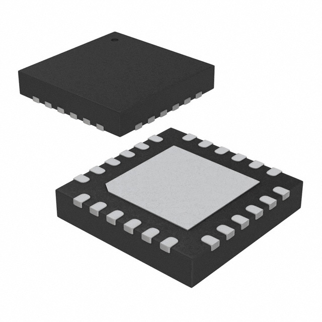


 工商网监
湘ICP备2023018690号
工商网监
湘ICP备2023018690号
