ADVANCED
LINEAR
DEVICES, INC.
ALD1704A/ALD1704B
ALD1704/ALD1704G
RAIL-TO-RAIL CMOS OPERATIONAL AMPLIFIER
GENERAL DESCRIPTION
FEATURES
The ALD1704A/ALD1704B/ALD1704/ALD1704G is a CMOS monolithic
operational amplifier with MOSFET input that has rail-to-rail input and
output voltage ranges. The input voltage range and output voltage range
are very close to the positive and negative power supply voltages.
Typically the input voltage can be beyond positive power supply voltage
V+, or the negative power supply voltage V- by up to 300mV. The output
voltage swings to within 60mV of either positive or negative power supply
voltages at rated load.
•
•
•
•
•
•
This device is designed as an alternative to the popular JFET input
operational amplifiers in applications where lower operating voltages,
such as 9V battery or ±3.25V to ±5V power supplies are being used. It
offers high slew rate of 5V/µs at low operating power of 30mW. Since the
ALD1704A/ALD1704B/ALD1704/ALD1704G is designed and manufactured with Advanced Linear Devices' standard enhanced ACMOS silicon
gate CMOS process, it also offers low unit cost and exceptional reliability.
•
•
•
•
•
The rail-to-rail input and output feature of the ALD1704A/ALD1704B/
ALD1704/ALD1704G allows a lower operating supply voltage for a given
signal voltage range and allows numerous analog serial stages to be
implemented without losing operating voltage margin. The output stage
is designed to drive up to 10mA into 400pF capacitive and 1.5KΩ resistive
loads at unity gain and up to 4000 pF at a gain of 5. Short circuit protection
to either ground or the power supply rails is at approximately 15mA clamp
current. Due to complementary output stage design, the output can both
source and sink 10mA into a load with symmetrical drive and is ideally
suited for applications where push-pull voltage drive is desired.
APPLICATIONS
The offset voltage is trimmed on-chip to eliminate the need for external
nulling in many applications. For precision applications, the output is
designed to settle to 0.1% in 2µs. For large signal buffer applications, the
operational amplifier can function as an ultra high input impedance
voltage follower/buffer that allows input and output voltage swings from
positive to negative supply voltages. This feature is intended to greatly
simplify systems design and eliminate higher voltage power supplies in
many applications. Additionally, robust design and rigorous screening
make this device especially suitable for operation in temperature-extreme environments and rugged conditions.
•
•
•
•
•
•
•
•
•
•
•
•
•
•
•
•
Rail-to-rail input and output voltage ranges
5.0V/µs slew rate
Output settles to 2mV of supply rails
High capacitive load capability -- up to 4000pF
Symmetrical push-pull output drives
No frequency compensation required -unity gain stable
Extremely low input bias currents -- 1.0pA
typical (20pAMax)
Ideal for high source impedance applications
High voltage gain -- typically 150V/mV
Output short circuit protected
Unity gain bandwidth of 2.1MHz
Suitable for rugged, temperature-extreme
environments
Voltage amplifier
Voltage follower/buffer
Charge integrator
Photodiode amplifier
Data acquisition systems
High performance portable
instruments
Signal conditioning circuits
Low leakage amplifiers
Active filters
Sample/Hold amplifier
Picoammeter
Current to voltage converter
Coaxial cable driver
Capacitive sensor amplifier
Piezoelectric transducer amplifier
PIN CONFIGURATION
ORDERING INFORMATION (“L” suffix denotes lead-free (RoHS))
Operating Temperature Range
0°C to +70°C
0°C to +70°C
-55°C to 125°C
8-Pin
Small Outline
Package (SOIC)
8-Pin
Plastic Dip
Package
8-Pin
CERDIP
Package
ALD1704ASAL
ALD1704BSAL
ALD1704SAL
ALD1704GSAL
ALD1704APAL
ALD1704BPAL
ALD1704PAL
ALD1704GPAL
ALD1704ADA
ALD17041BDA
ALD1704DA
ALD1704GDA
8
N/C
7
V+
3
6
OUT
4
5
N/C
N/C
1
-IN
2
+IN
V-
2
TOP VIEW
SAL, PAL, DA PACKAGES
* N/C pins are internally connected. Do not connect externally.
* Contact factory for leaded (non-RoHS) or extended high/low temperature versions.
Rev 2.1 ©2010 Advanced Linear Devices, Inc. 415 Tasman Drive, Sunnyvale, CA 94089-1706 Tel: (408) 747-1155 Fax: (408) 747-1286
www.aldinc.com
�ABSOLUTE MAXIMUM RATINGS
Supply voltage, V+
Differential input voltage range
Power dissipation
Operating temperature range SAL, PAL packages
DA package
Storage temperature range
Lead temperature, 10 seconds
CAUTION: ESD Sensitive Device. Use static control procedures in ESD controlled environment.
10.6V
-0.3V to V+ +0.3V
600 mW
0°C to +70°C
-55°C to +125°C
-65°C to +150°C
+260°C
OPERATING ELECTRICAL CHARACTERISTICS
TA = 25°C VS = ±5.0V unless otherwise specified
Parameter
Symbol Min
1704A
Typ
Max
Min
1704B
Typ
Max
±3.25
6.5
±5.0
10.0
Min
1704
Typ Max
Min
Supply
Voltage
VS
V+
Input Offset
Voltage
VOS
Input Offset
Current
IOS
1.0
15
240
1.0
15
240
1.0
15
240
Input Bias
Current
IB
1.0
20
300
1.0
20
300
1.0
Input Voltage
Range
VIR
Input
Resistance
RIN
Input Offset
Voltage Drift
TCVOS
Power Supply
Rejection Ratio
PSRR
70
80
65
80
65
80
60
Common Mode
Rejection Ratio
CMRR
70
83
65
83
65
83
Large Signal
Voltage Gain
AV
50
150
150
50
150
150
50
150
150
±3.25
6.5
±5.0
10.0
0.9
1.7
-5.3
+5.3
VO low
VO high
VO low
VO high
2.0
2.8
-5.3
+5.3
Dual Supply
Single Supply
10.0
11.0
mV
mV
RS ≤ 100KΩ
0°C ≤ TA ≤ +70°C
1.0
25
240
pA
pA
TA = 25°C
0°C ≤ TA ≤ +70°C
20
300
1.0
30
300
pA
pA
TA = 25°C
0°C ≤ TA ≤ +70°C
+5.3
±5.0
V
Ω
1012
1012
1012
5
5
5
7
40
-4.96 -4.90
4.95
-4.998 -4.99
4.99 4.998
4.90
40
-4.96
4.95
-4.998
4.99 4.998
-4.90
4.90
µV/°C
RS ≤ 100KΩ
80
dB
RS ≤ 100KΩ
0°C ≤ TA ≤ +70°C
60
83
dB
RS ≤ 100KΩ
0°C ≤ TA ≤ +70°C
32
150
150
V/ mV
V/ mV
V/ mV
RL = 10KΩ
No Load
0°C ≤ TA ≤ +70°C
V
RL = 10KΩ
0°C ≤ TA ≤ +70°C
RL =1MΩ
0°C ≤ TA ≤ +70°C
20
-4.96 -4.90
4.95
-4.998 -4.99
4.99 4.998
4.90
-4.99
Test
Conditions
V
V
±3.25
6.5
4.5
5.3
-5.3
Unit
±5.0
10.0
±5.0
10.0
1012
40
Output
Voltage
Range
±3.25
6.5
1704G
Typ
Max
4.90
4.99
-4.96 -4.90
4.95
-4.998 -4.99
4.998
V
Output Short
Circuit Current
ISC
15
Supply Current
IS
3.0
4.5
3.0
4.5
3.0
4.5
3.0
5.0
mA
VIN = 0V
No Load
Power
Dissipation
PD
30
45
30
45
30
45
30
50
mW
VS = ±5.0
No Load
Input
Capacitance
CIN
1
1
1
1
Bandwidth
BW
2.1
2.1
2.1
2.1
MHz
Slew Rate
SR
5.0
5.0
5.0
5.0
V/µs
AV = +1
RL = 2.0KΩ
Rise time
tr
0.1
0.1
0.1
0.1
µs
RL = 2.0KΩ
15
15
15
15
%
RL = 2.0KΩ
CL = 100pF
Overshoot
Factor
ALD1704A/ALD1704B
ALD1704/ALD1704G
15
15
Advanced Linear Devices
15
mA
pF
2 of 9
�OPERATING ELECTRICAL CHARACTERISTICS (cont'd)
TA = 25°C VS = ±5.0V unless otherwise specified
Min
1704B
Typ
Max
Min
1704
Typ
Max
Min
1704G
Typ Max
Symbol
Maximum Load
Capacitance
CL
400
4000
400
4000
400
4000
400
4000
Input Noise
Voltage
en
26
26
26
Input Current
Noise
in
0.6
0.6
ts
5.0
2.0
5.0
2.0
Settling
Time
Min
1704A
Typ
Max
Parameter
Unit
Test Conditions
pF
pF
Gain = 1
Gain = 5
26
nV/√Hz
f = 1KHZ
0.6
0.6
fA/√HZ
f = 10HZ
5.0
2.0
5.0
2.0
µs
µs
0.01%
0.1% AV = -1
RL = 5KΩ
CL = 50pF
VS = ±5.0V -55°C ≤ TA ≤ +125°C unless otherwise specified
Parameter
Symbol
1704ADA
Min
Typ Max
1704BDA
Min Typ
Max
Min
1704DA
Typ
Max
Unit
Test Conditions
RS ≤ 100KΩ
Input Offset Voltage
VOS
2.0
4.0
7.0
mV
Input Offset Current
IOS
8.0
8.0
8.0
nA
Input Bias Current
IB
10.0
10.0
10.0
nA
Power Supply
Rejection Ratio
PSRR
60
75
60
75
60
75
dB
RS ≤ 100KΩ
Common Mode
Rejection Ratio
CMRR
60
83
60
83
60
83
dB
RS ≤ 100KΩ
Large Signal
Voltage Gain
AV
30
125
30
125
30
125
V/mV
RL = 10KΩ
4.8
-4.9
4.9
4.8
-4.9
4.9
4.8
-4.9
4.9
V
V
RL = 10KΩ
RL = 10KΩ
Output Voltage
VO low
Range
VO high
ALD1704A/ALD1704B
ALD1704/ALD1704G
-4.8
-4.8
Advanced Linear Devices
-4.8
3 of 9
�Design & Operating Notes:
1. The ALD1704A/ALD1704B/ALD1704/ALD1704G CMOS operational
amplifier uses a 3 gain stage architecture and an improved frequency
compensation scheme to achieve large voltage gain, high output
driving capability, and better frequency stability. The ALD1704A/
ALD1704B/ALD1704/ALD1704G is internally compensated for unity
gain stability using a novel scheme that produces a clean single pole
roll off in the gain characteristics while providing for more than 70
degrees of phase margin at the unity gain frequency. A unity gain buffer
using the ALD1704A/ALD1704B/ALD1704/ALD1704G will typically
drive 400pF of external load capacitance without stability problems. In
the inverting unity gain configuration, it can drive up to 800pF of load
capacitance. Compared to other CMOS operational amplifiers, the
ALD1704A/ALD1704B/ALD1704/ALD1704G has shown itself to be
more resistant to parasitic oscillations.
2. The ALD1704A/ALD1704B/ALD1704/ALD1704G has complementary
p-channel and n-channel input differential stages connected in parallel
to accomplish rail to rail input common mode voltage range. This
means that with the ranges of common mode input voltage close to the
power supplies, one of the two differential stages is switched off
internally. To maintain compatibility with other operational amplifiers,
this switching point has been selected to be about 1.5V above the
negative supply voltage. Since offset voltage trimming on the ALD1704A/
ALD1704B/ALD1704/ALD1704G is made when the input voltage is
symmetrical to the supply voltages, this internal switching does not
affect a large variety of applications such as an inverting amplifier or
non-inverting amplifier with a gain larger than 2 (10V operation), where
the common mode voltage does not make excursions below this
switching point.
3. The input bias and offset currents are essentially input protection diode
reverse bias leakage currents, and are typically less than 1pA at room
temperature. This low input bias current assures that the analog signal
from the source will not be distorted by input bias currents. For
applications where source impedance is very high, it may be necessary
to limit noise and hum pickup through proper shielding.
4. The output stage consists of symmetrical class AB complementary
output drivers, capable of driving a low resistance load with up to 10mA
source current and 10mA sink current. The output voltage swing is
limited by the drain to source on-resistance of the output transistors as
determined by the bias circuitry, and the value of the load resistor.
When connected in the voltage follower configuration, the oscillation
resistant feature, combined with the rail-to-rail input and output feature,
makes the ALD1704A/ALD1704B/ALD1704/ALD1704G an effective
analog signal buffer for medium to high source impedance sensors,
transducers, and other circuit networks.
5. The ALD1704A/ALD1704B/ALD1704/ALD1704G operational amplifier has been designed to provide full static discharge protection.
Internally, the design has been carefully implemented to minimize latch
up. However, care must be exercised when handling the device to
avoid strong static fields that may degrade a diode junction, causing
increased input leakage currents. In using the operational amplifier, the
user is advised to power up the circuit before, or simultaneously with,
any input voltages applied and to limit input voltages to not exceed 0.3V
of the power supply voltage levels.
TYPICAL PERFORMANCE CHARACTERISTICS
COMMON MODE INPUT VOLTAGE RANGE
AS A FUNCTION OF SUPPLY VOLTAGE
OPEN LOOP VOLTAGE GAIN AS A FUNCTION
OF SUPPLY VOLTAGE AND TEMPERATURE
1000
±7
OPEN LOOP VOLTAGE
GAIN (V/mV)
COMMON MODE INPUT
VOLTAGE RANGE (V)
TA = 25°C
±6
±5
±4
±3
} +25°C
100
} +125°C
10
RL= 10KΩ
RL= 5KΩ
1
±2
±3
±2
±4
±5
±6
±7
0
±2
±4
±8
±6
SUPPLY VOLTAGE (V)
SUPPLY VOLTAGE (V)
INPUT BIAS CURRENT AS A FUNCTION
OF AMBIENT TEMPERATURE
SUPPLY CURRENT AS A FUNCTION
OF SUPPLY VOLTAGE
5
SUPPLY CURRENT (mA)
10000
INPUT BIAS CURRENT (pA)
} -55°C
VS = ±5.0V
1000
100
10
1.0
INPUTS GROUNDED
OUTPUT UNLOADED
4
3
TA = -55°C
-25°C
+25°C
2
1
+80°C
+125°C
0
0.1
-50
-25
0
25
50
75
100
125
ALD1704A/ALD1704B
ALD1704/ALD1704G
0
±1
±2
±3
±4
±5
±6
SUPPLY VOLTAGE (V)
AMBIENT TEMPERATURE (°C)
Advanced Linear Devices
4 of 9
�TYPICAL PERFORMANCE CHARACTERISTICS (cont'd)
OUTPUT VOLTAGE SWING AS A
FUNCTION OF SUPPLY VOLTAGE
OPEN LOOP VOLTAGE AS A
FUNCTION OF FREQUENCY
120
-55°C ≤ TA ≤ 125°C
100
OPEN LOOP VOLTAGE
GAIN (dB)
±6
RL = 10KΩ
RL = 10KΩ
±5
±4
RL = 2KΩ
±3
VS = ±5.0V
TA = 25°C
80
60
0
40
45
20
90
0
135
±2
0
±1
±2
±3
±4
±5
±6
180
-20
±7
1
SUPPLY VOLTAGE (V)
10
100
1K
10K
100K
1M
PHASE SHIFT IN DEGREES
OUTPUT VOLTAGE SWING (V)
±7
10M
FREQUENCY (Hz)
+5
+4
INPUT OFFSET VOLTAGE AS A FUNCTION
OF COMMON MODE INPUT VOLTAGE
15
INPUT OFFSET VOLTAGE (mV)
INPUT OFFSET VOLTAGE (mV)
INPUT OFFSET VOLTAGE AS A FUNCTION
OF AMBIENT TEMPERATURE
REPRESENTATIVE UNITS
VS = ±5.0V
+3
+2
+1
0
-1
-2
-3
-4
VS = ±5.0V
TA = 25°C
10
5
0
-5
-10
-15
-5
-50
-25
0
+25
+50
+75
-4
+100 +125
0
+2
+4
+6
VOLTAGE NOISE DENSITY AS A
FUNCTION OF FREQUENCY
OPEN LOOP VOLTAGE GAIN AS A FUNCTION
OF LOAD RESISTANCE
1000
150
100
VS = ±5.0V
TA = 25°C
10
VOLTAGE NOISE DENSITY
(nV/ √ Hz)
OPEN LOOP VOLTAGE
GAIN (V/mV)
-2
COMMON MODE INPUT VOLTAGE (V)
AMBIENT TEMPERATURE (°C)
1
125
VS = ±5.0V
TA = 25°C
100
75
50
25
0
1K
10K
100K
1000K
10
100
LOAD RESISTANCE (Ω)
10K
100K
1000K
SMALL - SIGNAL TRANSIENT
RESPONSE
LARGE - SIGNAL TRANSIENT
RESPONSE
5V/div
VS = ±5.0V
TA = 25°C
RL = 1KΩ
CL = 50pF
5V/div
2µs/div
ALD1704A/ALD1704B
ALD1704/ALD1704G
1K
FREQUENCY (Hz)
Advanced Linear Devices
100mV/div
50mV/div
VS = ± 5.0V
TA = 25°C
RL = 1.0KΩ
CL = 50pF
1µs/div
5 of 9
�TYPICAL APPLICATIONS
RAIL-TO-RAIL VOLTAGE FOLLOWER/BUFFER
RAIL-TO-RAIL VOLTAGE COMPARATOR
+12V
+10V
= 1012Ω
ZIN ~
0.1µF
VIN
CL
+
400pF
VIN
VOUT
+12V
VOUT
RL ≥ 1.5KΩ
0 ≤ VIN ≤ 10V
0.1µF
+
50K
10M
PHOTO DETECTOR CURRENT
TO VOLTAGE CONVERTER
LOW OFFSET SUMMING AMPLIFIER
RF = 5M
10K
50K
+5V
0.1µF
INPUT 1
I
-
INPUT 2
10K
VOUT
GAIN = 5
+
* Circuit Drives Large Load
Capacitance ≤ 4000pF
+5V
-
CL = 4000pF
RL ≥ 1.5K
+
-5V
-5V
0.1µF
WIEN BRIDGE OSCILLATOR (RAIL-TO -RAIL)
SINE WAVE GENERATOR
BANDPASS NETWORK
C2
R2
+5V
-
VOUT
+
C1
R1
VIN
+5V
-
10K
-5V
VOUT
+
.01µF
R = 10K
C = .01µF
VOUT = I X RF
PHOTODIODE
10K
Low Frequency
Breakpoint ƒL =
10K
1
~
~ 1.6K Hz
f=
=
2πRC
High Frequency
Cutoff ƒH =
LOW PASS FILTER (RFI FILTER)
RF
-5V
1
= 160Hz
2π R1 C1
R1 = 10K C1 = 100nF
R2 = 10K C2 = 500pF
1
= 32KHz
2π R2C2
PRECISION CHARGE INTEGRATOR
100K
1000pF
VIN
5K
5K
R1
R1
C1
+9V
-
0.02µF
+5V
1MΩ
VOUT
VIN
VOUT
+
+
-5V
Cutoff frequency =
1
= 3.2kHz
π R1C1
Gain = 10 Frequency roll-off 20dB/decade
ALD1704A/ALD1704B
ALD1704/ALD1704G
Advanced Linear Devices
6 of 9
�SOIC-8 PACKAGE DRAWING
8 Pin Plastic SOIC Package
E
Millimeters
Dim
S (45°)
D
A
Min
1.35
Max
1.75
Min
0.053
Max
0.069
A1
0.10
0.25
0.004
0.010
b
0.35
0.45
0.014
0.018
C
0.18
0.25
0.007
0.010
D-8
4.69
5.00
0.185
0.196
E
3.50
4.05
0.140
0.160
1.27 BSC
e
A
A1
e
Inches
0.050 BSC
H
5.70
6.30
0.224
0.248
L
0.60
0.937
0.024
0.037
ø
0°
8°
0°
8°
S
0.25
0.50
0.010
0.020
b
S (45°)
H
L
ALD1704A/ALD1704B
ALD1704/ALD1704G
C
ø
Advanced Linear Devices
7 of 9
�PDIP-8 PACKAGE DRAWING
8 Pin Plastic DIP Package
Millimeters
E
E1
D
S
A2
A1
e
b
A
L
Dim
Min
Max
Min
Max
A
3.81
5.08
0.105
0.200
A1
0.38
1.27
0.015
0.050
A2
1.27
2.03
0.050
0.080
b
0.89
1.65
0.035
0.065
b1
0.38
0.51
0.015
0.020
c
0.20
0.30
0.008
0.012
D-8
9.40
11.68
0.370
0.460
E
5.59
7.11
0.220
0.280
E1
7.62
8.26
0.300
0.325
e
2.29
2.79
0.090
0.110
e1
7.37
7.87
0.290
0.310
L
2.79
3.81
0.110
0.150
S-8
1.02
2.03
0.040
0.080
0°
15°
0°
15°
ø
b1
Inches
c
e1
ALD1704A/ALD1704B
ALD1704/ALD1704G
ø
Advanced Linear Devices
8 of 9
�CERDIP-8 PACKAGE DRAWING
8 Pin CERDIP Package
E E1
Millimeters
D
A1
s
A
L
L2
b
b1
e
L1
Inches
Dim
A
Min
Max
3.55
5.08
Min
0.140
Max
0.200
A1
1.27
2.16
0.050
0.085
b
0.97
1.65
0.038
0.065
b1
0.36
0.58
0.014
0.023
C
0.20
0.38
0.008
0.015
D-8
--
10.29
--
0.405
E
5.59
7.87
0.220
0.310
E1
7.73
8.26
0.290
0.325
e
2.54 BSC
0.100 BSC
e1
7.62 BSC
0.300 BSC
L
3.81
5.08
0.150
0.200
L1
3.18
--
0.125
--
L2
0.38
1.78
0.015
0.070
S
--
2.49
--
0.098
Ø
0°
15°
0°
15°
C
e1
ALD1704A/ALD1704B
ALD1704/ALD1704G
ø
Advanced Linear Devices
9 of 9
�
很抱歉,暂时无法提供与“ALD1704BPAL”相匹配的价格&库存,您可以联系我们找货
免费人工找货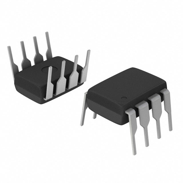


 工商网监
湘ICP备2023018690号
工商网监
湘ICP备2023018690号
