A1373 and A1374
High Precision, Output Pin Programmable
Linear Hall Effect Sensor ICs
Discontinued Product
These devices are no longer in production. The devices should not be
purchased for new design applications. Samples are no longer available.
Date of status change: October 31, 2011
Recommended Substitutions:
Contact Allegro Sales for more information.
NOTE: For detailed information on purchasing options, contact your
local Allegro field applications engineer or sales representative.
Allegro MicroSystems, Inc. reserves the right to make, from time to time, revisions to the anticipated product life cycle plan
for a product to accommodate changes in production capabilities, alternative product availabilities, or market demand. The
information included herein is believed to be accurate and reliable. However, Allegro MicroSystems, Inc. assumes no responsibility for its use; nor for any infringements of patents or other rights of third parties which may result from its use.
�A1373 and A1374
High Precision, Output Pin Programmable
Linear Hall Effect Sensor ICs
Features and Benefits
Description
▪
▪
▪
▪
▪
The A1373 and A1374 high precision linear Hall effect
sensor ICs are sensitive, temperature stable, linear devices
with externally programmable features. This device family
incorporates a chopper-stabilized amplifier, voltage regulator,
programming logic, and an output amplifier on a single IC.
The dynamic offset cancellation used with a chopperstabilization technique provides extremely low offset and
minimal temperature drift. A high frequency clock is used for
chopping, to ensure high frequency signal processing capability.
The A1373 and A1374 are ideal for use in automotive and
industrial linear position-sensing applications that require
increased reliability and accuracy over conventional contactingpotentiometer solutions. Key applications include: throttle
position sensors, pedal position sensors, and suspension height
sensors.
▪
▪
▪
▪
▪
▪
▪
▪
Output pin programming
Field-programmable for optimal application integration
Selectable coarse and fine gain and quiescent output voltage
Selectable sensitivity temperature coefficient
Selectable output clamp voltage level, including
no-clamp (rail-to-rail)
Selectable output polarity
Unipolar or bipolar operation
Ratiometric sensitivity, clamps, and quiescent output voltage
Chopper-stabilized Hall technique
Wide operating temperature range
On-chip regulator for over/under voltage protection
On-chip regulator provides EMI robustness
Wide lead-spacing with KB package
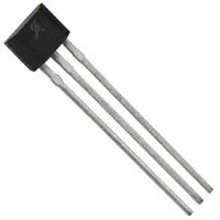
Package: 3 pin SIP (suffix KB)
The design and manufacturing flexibility of the A1373 and
A1374 complement the Allegro linear Hall effect family of
devices by offering programmable gain, quiescent offset voltage
for unipolar or bipolar operation, temperature coefficient,
clamps, and polarity. The device can be set up in a magnetic
circuit and programmed with a train of serial pulses via the output
Continued on the next page…
Not to scale
Functional Block Diagram
VCC
Pin 1
Voltage
Regulator
Amp
Filter
Dynamic Offset
Cancellation
To all subcircuits
Out
Hall drive circuit
Gain
Temperature
Coefficient
Trim Control
GND
Pin 2
A1373-DS, Rev. 12
Offset
VOUT
Pin 3
�High Precision, Output Pin Programmable
Linear Hall Effect Sensor ICs
A1373 and
A1374
Description (continued)
pin. Once the right combination of gain, quiescent output voltage, and
temperature coefficient has been selected, the codes can be locked
for one-time programming. In this manner, manufacturing tolerances
can be reduced and the assembly process can be simplified.
These devices are available in the KB package, a 3-pin SIP (single
inline package). The lead (Pb) free version has a 100% matte tin
plated leadframe.
Selection Guide
Ambient, TA
(ºC)
Packing*
Part Number
A1373EKB–T
Bulk, 500 pieces / bag
–40 to 85
A1373LKB–T
Bulk, 500 pieces / bag
–40 to 150
A1374EKB–T
Bulk, 500 pieces / bag
–40 to 85
A1374LKB–T
Bulk, 500 pieces / bag
–40 to 150
*Contact Allegro
for additional packing options.
Absolute Maximum Ratings
Characteristic
Symbol
Notes
Rating
Units
Supply Voltage
VCC
16
V
Reverse Supply Voltage
VRCC
–16
V
Output Voltage
VOUT
16
V
Reverse-Output Voltage
VROUT
–0.1
V
Output Source Current
Output Sink Current
IOUTSOURCE
3
mA
IOUTSINK
10
mA
Range E
–40 to 85
ºC
Range L
–40 to 150
ºC
TJ(max)
165
ºC
Tstg
–65 to 170
ºC
Operating Ambient Temperature
TA
Maximum Junction Temperature
Storage Temperature
When blowing fuses during device programming,
a voltage of 28 V may be applied to VOUT.
Allegro MicroSystems, Inc.
115 Northeast Cutoff
Worcester, Massachusetts 01615-0036 U.S.A.
1.508.853.5000; www.allegromicro.com
2
�High Precision, Output Pin Programmable
Linear Hall Effect Sensor ICs
A1373 and
A1374
CHARACTERISTIC PARAMETERS
Characteristic
Symbol
Test Conditions
Min.
Typ.
ELECTRICAL CHARACTERISTICS over operating temperature range, VCC= 5.0 V, unless otherwise noted
Operation within specification,
Supply Voltage
VCC
4.5
5.0
Tj < 165°C
Max
Units
5.5
V
–
8.2
10
mA
VCC = –16 V, TA = 25°C
–
–
16
mA
CLOAD = 10 nF, 90% full scale VOUT
–
–
300
μs
–
200
–
kHz
–
–
2.5
20
–
–
kHz
kHz
OUTPUT CHARACTERISTICS over operating temperature range, VCC= 5.0 V, unless otherwise noted
–
6
A1373 peak-to-peak, CLOAD > 1 nF,
Noise2,3
VN
A1374 2.5 mV/G
–
14
16
26
mV
mV
Supply Current
ICC
Reverse-Supply Current
IRCC
Power-On Time1
tPO
Chopping Frequency
fC
Internal Bandwidth
BW
Output Capacitance Load
CLOAD
Output Resistive Load
RLOAD
Phase Shift
∆Φ
VOUT(Sat)HIGH
Output Voltage
VOUT(Sat)LOW
Output Resistance
A1373
A1374
Small signal -3 dB
VOUT pin to GND pin
–
–
10
nF
4700
–
–
Ω
A1373
Magnetic signal freq. = 100 Hz
–
3
–
(°)
A1374
Magnetic signal freq. = 1000 Hz
–
3
–
(°)
4.65
4.7
–
V
–
0.2
0.25
V
–
1.5
–
Ω
–
20
–
G/μs
IOUTSOURCE = 1.2 mA,
B(kG) > (VCC–VOUT(Q)) / Sens (mV/G)
IOUTSINK = 1.2 mA,
B(kG) < VOUT(Q) / Sens (mV/G)
ROUT
MAGNETIC CHARACTERISTICS
Magnetic Slew Rate
SLR
V / ms / Sens
PRE-PROGRAMMING TARGET (Prior to coarse and fine trim) over operating temperature range, VCC= 5.0 V, unless
otherwise noted
Pre-Programming Quiescent
Output Voltage
Pre-Programming Sensitivity
Pre-Programming Sensitivity
Temperature Coefficient
VOUT(Q)PRE
SensPRE
TCPRE
B = 0 G, TA = 25°C
1.62
1.80
1.98
V
TA = 25°C
1.05
1.31
1.75
mV/G
–0.016
0.05
0.104
%/°C
TA relative to 25°C
INITIAL COARSE PROGRAMMING over operating temperature range, VCC= 5.0 V, unless otherwise noted
Initial Coarse Quiescent Output
Voltage
Initial Coarse Sensitivity
VOUT(Q)INITLOW
TA = 25°C
–
0.55
–
V
VOUT(Q)INITMID
Reference VOUT(Q)PRE
–
–-
–
V
VOUT(Q)INITHIGH
TA = 25°C
–
3.25
–
V
SensINITLOW
Reference SensPRE
–
–
–
mV/G
SensINITMID
TA = 25°C
–
2.8
–
mV/G
SensINITHIGH
TA = 25°C
–
5.5
–
mV/G
Continued on the next page...
Allegro MicroSystems, Inc.
115 Northeast Cutoff
Worcester, Massachusetts 01615-0036 U.S.A.
1.508.853.5000; www.allegromicro.com
3
�High Precision, Output Pin Programmable
Linear Hall Effect Sensor ICs
A1373 and
A1374
CHARACTERISTIC PARAMETERS (continued)
Characteristic
Symbol
Test Conditions
Min.
Typ.
Max
Units
QUIESCENT OUTPUT VOLTAGE PROGRAMMING over operating temperature range, VCC= 5.0 V, unless otherwise noted
VOUT(Q)LOW
0.7
–
1.9
V
Quiescent Output Voltage Range
VOUT(Q)MID
B = 0 G, TA = 25°C
2.0
–
3.2
V
VOUT(Q)HIGH
3.5
–
4.5
V
Average Quiescent Output Voltage
StepVOUT(Q)
TA = 25°C
3.0
3.275
3.5
mV
Step Size4,5,6
Quiescent Output Voltage
Fine programming value selection
±0.5 ×
ErrPROGVOUT(Q)
–
–
mV
StepVOUT(Q)
Programming Resolution
accuracy
Quiescent Output Voltage Drift
Over Operating Temperature
Range
Quiescent Output Voltage
Programming Bits
ΔVOUT(Q)
–
VOUTCLP10HIGH
10% Output Clamp Option7
VOUTCLP10LOW
VOUTCLP20HIGH
20% Output Clamp
Option7
VOUTCLP20LOW
Delay to Clamp
tCLP
VOUT(Q) = VOUT(Q)LOW
–
–
±40
mV
VOUT(Q) = VOUT(Q)MID
–
–
±40
mV
VOUT(Q) = VOUT(Q)HIGH
–
–
±55
mV
–
–
4.350
4.300
0.4
0.3
3.925
3.900
0.9
0.8
–
–
2
9
–
–
–
–
–
–
–
–
–
–
–
–
4.565
4.650
0.6
0.6
4.125
4.200
1.1
1.1
2
100
Bit
Bit
V
V
V
V
V
V
V
V
μs
μs
2.8
5.7
11.25
14
28
56
mV/G
mV/G
mV/G
μV/G
μV/G
μV/G
–
μV/G
Coarse (Range selection)
Fine (Value selection)
A1373
High-side output clamp
A1374
A1373
Low-side output clamp
A1374
A1373
High-side output clamp
A1374
A1373
Low-side output clamp
A1374
A1373
A1374
SENSITIVITY PROGRAMMING over operating temperature range, VCC= 5.0 V, unless otherwise noted
SensLOW
1.75
–
Sensitivity Range8
SensMID
TA = 25°C
3.5
–
SensHIGH
7.0
–
StepSENSLOW
6
9.5
Average Sensitivity Step Size4,5,6
StepSENSMID
TA = 25°C
12
18.7
StepSENSHIGH
22
37.0
Sensitivity Programming
Resolution
Sensitivity Programming Bits
Fine programming value selection
accuracy
–
–
Coarse (Range selection)
Fine (Value selection)
–
–
2
8
–
–
Bit
Bit
–
Negative Sensitivity
–
1
–
Bit
ErrPROGSENS
±0.5 ×
StepSENS
POLARITY PROGRAMMING
Polarity Programming Bit
Continued on the next page...
Allegro MicroSystems, Inc.
115 Northeast Cutoff
Worcester, Massachusetts 01615-0036 U.S.A.
1.508.853.5000; www.allegromicro.com
4
�High Precision, Output Pin Programmable
Linear Hall Effect Sensor ICs
A1373 and
A1374
CHARACTERISTIC PARAMETERS (continued)
Characteristic
Symbol
Test Conditions
Min.
Typ.
Max
Units
SENSITIVITY TEMPERATURE COEFFICIENT PROGRAMMING over operating temperature range, VCC= 5.0 V, unless
otherwise noted
Sensitivity Temperature
Coefficient Range
TC
Sensitivity T/C codes 0 to 11,
minimum (absolute) positive
temperature coefficient attainable
Sensitivity T/C codes 16 to 27,
minimum (absolute) negative
temperature coefficient attainable
Average Sensitivity
StepTC
Temperature Coefficient Step
TA = 150C
5
6
4,
,
Size
Sensitivity Temperature
–
Coefficient Programming Bits
ONE-TIME PROGRAMMING
–
Device Programming Lock Bit
RATIOMETRY over operating temperature range, VCC= 5.0 V, unless otherwise noted
RatVOUT(Q)
Quiescent Voltage Error
VCC at VOPERATING
RatSENS
Sensitivity Error
VCC at VOPERATING
Clamp Error
RatVOUTCLP
VCC at VOPERATING
LINEARITY over operating temperature range, VCC= 5.0 V, unless otherwise noted
Positive Linearity Error
Lin+
VCC at VOPERATING
Lin–
Negative Linearity Error
VCC at VOPERATING
SYMMETRY over operating temperature range, VCC= 5.0 V, unless otherwise noted
Sym
Symmetry Error
VCC at VOPERATING – VCC
ADDITIONAL CHARACTERISTICS
Sensitivity Drift9
Package Thermal Resistance
ΔSens
RθJA
1 layer PCB with copper limited to
solder pads; see Allegro web site for
additional thermal information
–
0.07
–
%/°C
–
–0.016
–
%/°C
–
0.01
–
%/°C
–
5
–
Bit
–
1
–
Bit
–
±0.25
±1.0
±1.5
–
%
–
%
–
%
±0.5
±0.5
–
%
–
–
%
–
±0.35
–
%
–
–
±2
%
–
177
–
°C/W
–
–
18
4
mA
mA
–
–
–
FAULT CONDITIONS over operating temperature range, VCC= 5.0 V, unless otherwise noted
VOUT pin to VCC pin
–
IOUTSHT
Shorted Output Wire
VOUT pin to GND pin
–
1
tPO does not include tCLP , specified in the Quiescent Programming section of this table.
Peak to peak value exceeded: 0.3% (6σ).
3 For A1373, no digital noise is present at the output.
4 Step size is larger than required for the specified range, to take into account manufacturing spread.
5 Individual code step sizes can be greater than 2× larger than the step size at each significant bit rollover.
6 Average fine code step size in a given range = (Output value at highest fine code in the range – Output value at code 0 of the range) / Total quantity of
steps (codes) in the range.
7 Values indicated are valid if any additional magnetic field does not exceed B(kG)= ±2 (V) / Sens (mv/G), after V
OUTCLP is reached.
8 Program the Sensitivity T/C register before programming Sensitivity Coarse and Sensitivity Fine, due to a worst case shift of ±3% in sensitivity at 25°C
at the maximum values for Sensitivity T/C: Positive T/C and Sensitivity T/C: Negative T/C. The Programming Guidelines section in this document lists a
complete recommended order for programming individual values.
9Drift due to temperature cycling is due to package effects on the Hall transducer. The stress is reduced when the package is baked. However, it will
recover over time after removal from the bake.
2
Allegro MicroSystems, Inc.
115 Northeast Cutoff
Worcester, Massachusetts 01615-0036 U.S.A.
1.508.853.5000; www.allegromicro.com
5
�High Precision, Output Pin Programmable
Linear Hall Effect Sensor ICs
A1373 and
A1374
Typical Characteristics
Temperature Coefficient Code Profile
TA = 150°C, Magnetically Back-Biased
VOUT(Q) = VOUT(Q)PRE, Sens = 5 mV/G
3.4
3.2
Positive Programming Codes
VOUT(Q) (V)
3.0
Negative Programming Codes
2.8
2.6
2.4
2.2
2.0
0
5
10
15
20
25
30
Sensitivity TC Code
Code
0
1 – 11
12 – 15
16 – 27
28 – 31
Application
Initial code
Positive TC codes, use to increase TC value
[Unused, same effect as 4 – 7, respectively]
Negative TC codes, use to decrease TC value
[Unused, same effect as 20 – 23, respectively]
Allegro MicroSystems, Inc.
115 Northeast Cutoff
Worcester, Massachusetts 01615-0036 U.S.A.
1.508.853.5000; www.allegromicro.com
6
�High Precision, Output Pin Programmable
Linear Hall Effect Sensor ICs
A1373 and
A1374
Sensitivity Temperature Coefficient Range, TC
0.25
0.20
Typical maximum attainable
positive TC programming range
0.15
Extended Range Not Guaranteed
TCPRE(max)
0.10
A
TC (% / °C)
TC(typ), for positive programming
0.05
Guaranteed Programmable Range
0
TC Range Before Programming
TC(typ), for negative programming
TCPRE(min)
–0.05
Extended Range Not Guaranteed
–0.10
Typical maximum attainable
negative TC programming range
–0.15
A
–0.20
Units with a TC in the range TC(min) < TC < TCPRE(max)
before programming may not be programmable
to the maximum attainable negative TC programming value
–0.25
Allegro MicroSystems, Inc.
115 Northeast Cutoff
Worcester, Massachusetts 01615-0036 U.S.A.
1.508.853.5000; www.allegromicro.com
7
�High Precision, Output Pin Programmable
Linear Hall Effect Sensor ICs
A1373 and
A1374
Average Supply Current (Icc) vs Temperature
Vcc = 5V
10.0
Average Supply Current (mA)
9.5
9.0
8.5
8.0
7.5
7.0
6.5
6.0
5.5
5.0
-50
-25
0
25
50
75
100
125
150
Temperature (°C)
Average Ratiometry, Voq
Average Ratiometry, Sens
101.0
Average Ratiometry (Sens) (%)
Average Ratiometry (Voq) (%)
101.0
100.8
4.5 to 5.0 V
100.6
5.5 to 5.0 V
100.4
100.2
100.0
99.8
99.6
99.4
99.2
99.0
-50
100.8
4.5 to 5.0 V
100.6
5.5 to 5.0 V
100.4
100.2
100.0
99.8
99.6
99.4
99.2
99.0
-25
0
25
50
75
100
125
-50
150
-25
0
101.0
101.0
100.8
100.8
100.6
100.6
Average Linearity (%)
Average Symmetry (%)
50
75
100
125
150
Average Linearity vs Temperature
Average Symmetry vs Temperature
Linearity +
Linearity -
100.4
100.4
100.2
100.2
100.0
100.0
99.8
99.6
99.8
99.6
99.4
99.4
99.2
99.2
99.0
99.0
-50
25
Temperature (°C)
Temperature (°C)
-25
0
25
50
Temperature (°C)
75
100
125
150
-50
-25
0
25
50
75
100
125
150
Temperature (°C)
Allegro MicroSystems, Inc.
115 Northeast Cutoff
Worcester, Massachusetts 01615-0036 U.S.A.
1.508.853.5000; www.allegromicro.com
8
�High Precision, Output Pin Programmable
Linear Hall Effect Sensor ICs
A1373 and
A1374
Average Delta Sensitivity
(percent change relative to 25°C)
Average Delta Sensitivity over TC Codes
(percent change relative to 25°C)
Initial Coarse Range
25
Sensitivity Low
6
Initial Delta Sensitivity (%)
Average Delta Sensitivity (%)
8
Sensitivity Mid
Sensitivity High
4
2
0
-2
-4
-6
20
Sensitivity Low - TC Code 0
Sensitivity Low - TC Code 11
15
Sensitivity Low - TC Code 27
10
5
0
-5
-10
-50
-25
0
25
50
75
Temperature (°C)
100
125
-15
150
-50
-25
Average Delta Sensitivity
(percent per degree Celsius change relative to 25°C)
Average Delta Sensitvity (%/°C)
Average Delta Sensitvity (%/°C)
50
75
Temperature (°C)
100
125
150
0.20
0.06
Sensitivity Low
Sensitivity Mid
0.04
Sensitivity High
0.02
0
-0.02
-0.04
-0.06
Sensitivity Low - TC Code 0
0.15
Sensitivity Low - TC Code 11
Sensitivity Low - TC Code 27
0.10
0.05
0
-0.05
-0.10
-0.15
-50
-25
0
25
50
75
Temperature (°C)
100
125
150
-0.20
-50
0
25
50
75
Temperature (°C)
100
125
150
10
15
TC Code 1
TC Code 2
TC Code 4
TC Code 8
TC Code 11
5
TC Contribution to Delta
Sensitivity (%)
10
5
0
-5
-10
-25
Negative TC Contribution to Delta Sensitivity
Positive TC Contribution to Delta Sensitivity
TC Contribution to
Delta Sensitivity (%)
25
Average Delta Sensitivity
(percent per degree Celsius change relative to 25°C)
Initial Coarse Low
0.08
-0.08
0
-50
-25
0
25
50
75
Temperature (°C)
100
125
150
0
TC Code 16
TC Code 17
TC Code 18
TC Code 20
TC Code 24
TC Code 27
-5
-10
-15
-20
-50
-25
0
25
50
75
Temperature (°C)
100
125
150
Allegro MicroSystems, Inc.
115 Northeast Cutoff
Worcester, Massachusetts 01615-0036 U.S.A.
1.508.853.5000; www.allegromicro.com
9
�High Precision, Output Pin Programmable
Linear Hall Effect Sensor ICs
A1373 and
A1374
Average Quiescent Output Voltage
Average Delta Quiescent Output Voltage
Relative to 25°C, Initial Sensitivity
3.5
6
Vout(q)Low - Initial
Vout(q)Mid - Initial
Vout(q)High - Initial
2.5
2.0
1.5
1.0
0.5
0
-50
4
Average Delta Vout(q) (mV)
Average Vout(q) (V)
3.0
2
0
-2
-4
Vout(q)Low
Vout(q)Mid
Vout(q)High
-6
-8
-10
-25
0
25
50
75
Temperature (°C)
100
125
150
-50
25
50
75
100
125
150
Average Initial Quiescent Output Voltage vs Supply Voltage
TA = 25°C
6
4.0
5
Average Vout(q) (V)
3.5
4
3
2
1
Vout(q)Low - Initial
Vout(q)Mid - Initial
Vout(q)High - Initial
3.0
2.5
2.0
1.5
1.0
Vout(q)Low - Max Code
Vout(q)Mid - Max Code
Vout(q)High - Max Code
0.5
0
-25
0
25
50
75
100
125
150
4
4.5
Temperature (°C)
5
Supply Voltage (V)
5.5
6
Average Quiescent Output Voltage over Sensitivity
1.85
1.83
Average Vout(q) (V)
Average Vout(q) (max Code - 511) (V)
0
Temperature (°C)
Average Quiescent Output Voltage
Max Code (511)
0
-50
-25
Vout(q)Mid - SensLow
Vout(q)Mid - SensMid
Vout(q)Mid - SensHigh
1.81
1.79
1.77
1.75
-50
-25
0
25
50
75
100
125
150
Temperature (°C)
Allegro MicroSystems, Inc.
115 Northeast Cutoff
Worcester, Massachusetts 01615-0036 U.S.A.
1.508.853.5000; www.allegromicro.com
10
�High Precision, Output Pin Programmable
Linear Hall Effect Sensor ICs
A1373 and
A1374
Average Saturation Voltage
Average Clamp Values
5
Average Clamp Voltage (V)
5
VOUT(sat) (V)
4
3
VOUT(sat)+
2
VOUT(sat)–
1
4
10% High Clamp
3
10% Low Clamp
20% High Clamp
2
20% Low Clamp
1
0
0
-50
-25
0
25
50
75
Temperature (°C)
100
125
150
-50
-25
0
25
50
75
100
125
150
Temperature (°C)
Allegro MicroSystems, Inc.
115 Northeast Cutoff
Worcester, Massachusetts 01615-0036 U.S.A.
1.508.853.5000; www.allegromicro.com
11
�High Precision, Output Pin Programmable
Linear Hall Effect Sensor ICs
A1373 and
A1374
Chopper Stabilization Technique
pass through a low-pass filter, while the modulated dc offset is
suppressed.
Chopper stabilization is a unique approach used to minimize
Hall offset on the chip. The patented Allegro technique, namely
Dynamic Quadrature Offset Cancellation, removes key sources
of the output drift induced by thermal and mechanical stresses.
This offset reduction technique is based on a signal modulationdemodulation process. The undesired offset signal is separated
from the magnetic field-induced signal in the frequency domain,
through modulation.
The chopper stabilization technique uses a 200 kHz high
frequency clock. For demodulation process, a sample and hold
technique is used, where the sampling is performed at twice the
chopper frequency (400 kHz). This high-frequency operation
allows a greater sampling rate, which results in higher accuracy
and faster signal-processing capability.
The subsequent demodulation acts as a modulation process for
the offset, causing the magnetic field-induced signal to recover
its original spectrum at baseband, while the dc offset becomes
a high-frequency signal. The magnetic-sourced signal then can
This approach desensitizes the chip to the effects of thermal and
mechanical stresses, and produces devices that have extremely
stable quiescent Hall output voltages and precise recoverability
after temperature cycling. This technique is made possible
through the use of a BiCMOS process, which allows the use of
low-offset, low-noise amplifiers in combination with high-density logic integration and sample-and-hold circuits.
Regulator
Hall Element
Amp
Sample and
Hold
Clock/Logic
Low-Pass
Filter
Concept of Chopper Stabilization Technique
Allegro MicroSystems, Inc.
115 Northeast Cutoff
Worcester, Massachusetts 01615-0036 U.S.A.
1.508.853.5000; www.allegromicro.com
12
�High Precision, Output Pin Programmable
Linear Hall Effect Sensor ICs
A1373 and
A1374
Definitions of Terms
Linear: A type of Hall-Effect device that produces an analog output
voltage proportional to the strength of a sensed magnetic field.
bit (fuse) has been blown, it cannot be reset. The terms trimming and
programming can be used interchangeably with blowing in this context.
Ratiometric: A linear Hall-Effect device that, when not subjected
to a significant magnetic field, has an output that is a ratio of its supply
voltage. A ratiometric performance of 100% indicates the output follows
the supply with no percentage error.
Programming modes: Testing the results is the only valid method
Gauss: Standard unit of measuring magnetic flux density. 1 gauss is
Mode Selection State.
to guarantee successful programming, and multiple modes are provided
to support this. The programming modes are described in the section
equal to 1 Maxwell per square centimeter or 10-4 tesla. (For reference,
the earth’s magnetic field is approximately 0.5 gauss.)
Code: The number used to identify the register and the bitfield to be
Blowing: Applying a pulse of sufficient voltage and duration to
permanently set a bit, by blowing a fuse internal to the device. Once a
programmed, expressed as the decimal equivalent of the binary value.
The LSB of a register is denoted as bit 0.
Typical Application Drawing
VREG
1
VCC
A1373
A1374
CBYPASS
0.1 μF
GND
2
Output
VOUT 3
RLOAD
4.7 k7
CLOAD
1 nF
Allegro MicroSystems, Inc.
115 Northeast Cutoff
Worcester, Massachusetts 01615-0036 U.S.A.
1.508.853.5000; www.allegromicro.com
13
�High Precision, Output Pin Programmable
Linear Hall Effect Sensor ICs
A1373 and
A1374
Characteristic Definitions
Quiescent Output Voltage. In the quiescent state (no significant magnetic field: B = 0), the output, VOUTQ, equals a ratio of
the supply voltage, VCC, throughout the entire operating ranges
of VCC and ambient temperature, TA. Due to internal component
tolerances and thermal considerations, there is a tolerance on the
quiescent output voltage, ∆VOUTQ, which is a function of both
∆VCC and ∆TA. For purposes of specification, the quiescent output voltage as a function of temperature, ∆VOUTQ(∆TA), is defined
as:
ΔVOUTQ(ΔΤΑ) =
VOUTQ(ΤΑ) – VOUTQ(25ºC)
(1)
Sens(25ºC)
The ratiometric change in the quiescent output voltage,
RATVOUT(Q) (%), is defined as:
RATVOUT(Q) =
Sensitivity. The presence of a south-polarity (+B) magnetic
field, perpendicular to the branded face of the device package,
increases the output voltage, VOUT, in proportion to the magnetic
field applied, from VOUTQ toward the VCC rail. Conversely, the
application of a north polarity (–B) magnetic field, in the same
orientation, proportionally decreases the output voltage from its
quiescent value. This proportionality is specified as the magnetic
sensitivity of the device and is defined as:
RATSens =
RATVCLP =
Lin– =
Sens(ΤΑ) – Sens(25ºC)
Sens(25ºC)
× 100%
5V
× 100%
(4)
Sens(VCC)
Sens(5V)
VCC
5V
× 100%
(5)
(3)
Ratiometric. The A1373 and A1374 feature ratiometric
output. This means that the quiescent voltage output, VOUTQ,
VCLP(VCC)
VCC
VCLP(5V)
5V
× 100%
(6)
Linearity and Symmetry. The on-chip output stage is
designed to provide linear output at a supply voltage of 5 V.
Although the application of very high magnetic fields does not
damage these devices, it does force their output into a nonlinear
region. Linearity in percent is measured and defined as:
The stability of the device magnetic sensitivity as a function of
ambient temperature, ∆ Sens (∆TA) (%) is defined as:
ΔSens(ΔΤΑ) =
VCC
Note that clamping effect is applicable only when clamping is
enabled by programming of the device.
Lin+ =
2B
VOUTQ(5V)
the ratiometric change in sensitivity is defined as:
(2)
Sens =
VOUTQ(VCC)
and the ratiometric change in clamp voltage is defined as:
where Sens is in mV/G, and the result is the device equivalent
accuracy, in gauss (G), applicable over the entire operating temperature range.
VOUT(–B) – VOUT(+B)
magnetic sensitivity, Sens, and clamp voltage, VOUTCLP , are
proportional to the supply voltage, VCC.
VOUT(+B) – VOUTQ
��VOUT(+B½)– VOUTQ
VOUT(–B) – VOUTQ
2(VOUT(–B½) – VOUTQ)
¾���%
× 100%
(7)
(8)
and output symmetry as:
Sym =
VOUT(+B) – VOUTQ
VOUTQ – VOUT(–B)
× 100%
Allegro MicroSystems, Inc.
115 Northeast Cutoff
Worcester, Massachusetts 01615-0036 U.S.A.
1.508.853.5000; www.allegromicro.com
(9)
14
�High Precision, Output Pin Programmable
Linear Hall Effect Sensor ICs
A1373 and
A1374
Pulse Generation
Several parameters can be field-programmed. To do so, a coded
series of voltage pulses through the VOUT pin is used to set
bitfields in onboard registers. The effect on the device output can
be monitored, and the registers can be cleared and set repeatedly
until the required output results are achieved. To make the setting
permanent, bitfield-level solid state fuses are blown, and finally,
a device-level fuse is blown, blocking any further coding.
Although any programmable variable power supply can be
used to generate the pulsed waveforms, Allegro highly recommends using the Allegro Sensor IC Evaluation Kit, available on
the Allegro Web site On-line Store. The manual for that kit is
available for download free of charge, and provides additional
information on programming these devices.
There are three voltage levels that must be taken into account
when programming. For purposes of explanation in this document, the signal levels are referred to simply as high programming voltage, VPH , mid, VPM , and low, VPL .
The rising edge of the high level, VPH , pulse generates a state
change. The falling edge of the high level, VPH , pulse increments
the mode, register, or bitfield selection by one, when allowed to
drop below the low level, VPL , threshold. A delay on the falling edge, at the mid level, VPM , range is required to guarantee
proper programming level recognition. When it is not desirable to
increment these fields further, it is acceptable to hold the signal
at the mid level, VPM , range and then transition to another high
level, VPH, pulse. Referring to the Programming State Machine
diagram, when using Blow Fuse mode the fourth high level, VPH ,
pulse (including the key sequence to enable Blow Fuse mode),
will blow the selected key-code combination. If fuse blowing is
not desired, it is recommended to reset the A137x by toggling the
supply pin. If the high level, VPH, pulse is not generated, and the
A137x is not reset, then the next key sequence to change states
will blow the unwanted key-code combination. For multiple
register addressing without fuse blowing, Try Value mode must
be used.
PROGRAMMING PROTOCOL CHARACTERISTICS, over operating temperature range, unless otherwise noted
Characteristic
Symbol
Programming Current2
Pulse Width
Min.
Typ.
Max.
Units
0
–
5
V
14
–
16
V
VPH
Low voltage range, for addressing registers and
bitfields
Mid voltage range, for addressing bitfields and for
separating programming signals
High voltage range, for enabling state changes
and for fuse blowing
25
26
27
V
IPP
tr = 11 μs; 5 V → 28 V; CPROG = 0.1 μF
–
209
–
mA
tPHE
High pulse duration for enabling state change
20
–
–
μs
tPHP
High pulse duration for blowing fuses
100
–
–
μs
tPLA
Low pulse duration for bitfield addressing
6
–
–
μs
tPME
Mid pulse delay on falling edge of high pulse, VPH
15
–
–
μs
tPMA
Mid pulse duration for bitfield addressing
6
–
–
μs
VPL
Programming Voltage1
Test Conditions
VPM
VPL to VPH or VPM; maximum may be application
5
–
100
dependent
VPH or VPM to VPL; maximum may be application
Pulse Fall Time
tf
5
–
100
dependent
1Programming voltages are measured at pin #3, VOUT, of the A137x.
2A minimum capacitance of 0.1 μF must be connected from VOUT to the GND pin of the A137x in order to provide the current
necessary to blow the fuse.
Pulse Rise Time
tr
Allegro MicroSystems, Inc.
115 Northeast Cutoff
Worcester, Massachusetts 01615-0036 U.S.A.
1.508.853.5000; www.allegromicro.com
μs
μs
15
�High Precision, Output Pin Programmable
Linear Hall Effect Sensor ICs
A1373 and
A1374
The mid voltage range, VPM , is a neutral level used to separate
VPH and VPL pulses from each other.
required, then the output drive signal must be released to allow
the output level to be read for each bitfield increment (see panels
A and B, below).
The low level, VPL, pulse is used to increment the mode, register,
and bitfield addresses that are to be set. The device generates a
VPL pulse on the falling edge of the mid-level to low-level transition, VPM to VPL.
To guarantee proper pulse recognition, each level must be held
for the predefined durations specified in the Programming Protocol Characteristics table. Failure to follow the specifications may
produce undefined results. Examples of common pulse trains are
shown in panels C and D, below.
In Try Value mode,the programming drive signal can be held
at 5 V or less if no code search is required. If a code search is
Mode Select Register Select
(Code 1)
(Code 3)
Bitfield Select
(Code 10)
Mode Select Register Select
(Code 3)
(Code 1)
Mode Select
(Code 1)
30
Bitfield Select
(Code 10)
Mode Select
(Code 1)
30
}V
}V
PH
PH
25
= Programming edge
20
tPLA
tPME
15
tPMA
}V
PM
tPHE
10
1
1
2
3
1
2
3
4
5
6
7
8
9
10
Programming Level (V)
Removing the output drive signal after each
VPM allows measurement of the output pin
20
}V
15
PM
10
1
1
5
1
2
3
1
2
3
4
5
6
7
8
10
9
1
5
Time (μs)
Register Select
(Code 3)
VPL
Bitfield Select
(Code 8)
B. Try Value Mode. Code search with drive signal released
after each VPM, allows output to be measured after each code
increment.
Blow Fuse
Mode Select
(Code 3)
30
Register Select Bitfield Select
(Code 0)
(Code 1)
Lock (blow Lock Bit fuse)
30
}V
}V
PH
Programming Level (V)
Blow
Fuse
mode
selected
20
PH
25
Sensitivity
Fine
register
selected
Bitfield 8
address
selected
Lock
Device
mode
selected
Programming Level (V)
25
20
}V
15
PM
10
tPME
tPLA tPMA
}V
15
PM
tPHE
tPHP
10
1
2
1
2
3
1
2
3
4
5
6
7
1
8
5
2
3
1
5
0
1
Holding at VPM is allowed when no
VPL is required; dropping to VPL
will increment by 1 bitfield
VPL
VPL
Time (μs)
C. Blow Fuse Mode: Code 8 / bit 4 is programmed.
800
750
700
650
600
550
500
450
400
350
300
250
200
150
100
50
0
1350
1300
1200
1250
1150
1100
1050
1000
950
900
850
800
750
700
650
600
550
500
450
400
350
300
250
200
150
50
0
100
0
1350
1300
1250
1200
2.0
1150
1100
1050
950
1000
900
850
800
750
700
2.6 2.7 2.8 2.9 3.0
Time (μs)
A. Try Value Mode. Code search with drive signal held
at 5 V.
Mode Select
(Code 2)
650
2.2 2.3 2.4 2.5
600
500
450
400
350
200
150
300
VOUT measurements 2.1
2.0
0
1350
1300
1200
1250
1150
1100
1050
950
1000
900
850
0
550
VPL
250
Try Mode
selected
50
10th address
selected
800
750
700
650
600
550
500
450
350
300
250
200
150
50
100
0
0
400
Sensitivity Fine selected
(Sensitivity Coarse)
(Qvo Fine)
Try Mode
selected
100
Programming Level (V)
25
Time (us)
D. Lock Device Mode. Device-level Lock Bit is programmed;
device programming is then permanently disabled.
Allegro MicroSystems, Inc.
115 Northeast Cutoff
Worcester, Massachusetts 01615-0036 U.S.A.
1.508.853.5000; www.allegromicro.com
16
�High Precision, Output Pin Programmable
Linear Hall Effect Sensor ICs
A1373 and
A1374
Programming State Machine
POWER UP
INITIAL STATE
VPH
VPH
MODE SELECT
VPL
VPL
TRY
1
VPL
BLOW
2
VPH
VPL
LOCK
3
VPH
VPH
REGISTER SELECT
VPL
QVO
VPL
Coarse
0
VPH
QVO
Fine
1
VPL
SENS.
VPL
Coarse
2
VPH
SENS.
Fine
3
VPH
VPL
VPH
0
VPH
VPL
[Optional:
Measure]
1
VPL
VPH
VPL
VPH
BITFIELD SELECT
[Optional:
Measure]
SENS.
TC
4
VPH
BLOW
OR LOCK
MODE?
6
VPH
[Optional:
Measure]
2
POLAR
[Write Mode]
VPL
2^N -1
VPL
VPH
No
CLAMP VPL
5
VPH
Yes
FUSE BLOWING
User generated transition
Internally generated transition
Allegro MicroSystems, Inc.
115 Northeast Cutoff
Worcester, Massachusetts 01615-0036 U.S.A.
1.508.853.5000; www.allegromicro.com
17
�High Precision, Output Pin Programmable
Linear Hall Effect Sensor ICs
A1373 and
A1374
Programming Protocol and State Machine Description
INITIAL STATE
After system power-up, the programming logic is reset to a
known state. This is referred to as the Initial state. All the registers that have intact fuses are set to logic 0.
While in the Initial state, any VPL pulses on the VOUT pin are
ignored.
To enter the Mode Selection state, send one VPH pulse on the
VOUT pin.
MODE SELECTION STATE
This state allows the selection of the programming mode:
• Sens. Fine. Register for setting the value within the range set in the
Sens. Coarse register (8 bits)
• [Sensitivity] TC Register. Register for setting the temperature coefficient for the device (5 bits).
• Clamp [VOUTCLP] Bit. Register for setting the clamping voltage of
the output (2 bits)
• Polarity Bit. Register setting the polarity of the output (1 bit)
To select a register, increment through the register bitfields by
sending VPL pulses on the VOUT pin. Note that the programming of registers should follow the order shown in item 7 in the
section Programming Guidelines, not the bitfield selection order
shown here. The bitfield selection order is:
• Try Value Mode. In this mode, the user provisionally downloads
settings to the device registers, without blowing the bits. The user
can increment through the codes of each parameter, and evaluate the
results of various code settings.
• Blow Fuse Mode. In this mode, after downloading the settings, the
user can blow the fuses in specific registers.
• Lock Device Mode. This mode is similar to Blow Fuse mode, except
that the fuse that is blown permanently prevents any further programming of any bits in the device.
This register wraps by default.
To select a mode, increment through the register bitfields by
sending VPL pulses on the VOUT pin, as follows:
To enter the Bitfield Selection state, send one VPH pulse on the
VOUT pin.
0 pulses – No effect
1 pulse – Try Value mode
2 pulses – Blow Fuse mode
3 pulses – Lock Device mode
This register wraps by default. This means that sending additional VPL pulses traverses the register again.
Any VPH pulse sent before a VPL pulse has no effect.
To enter the Register Selection state, after sending a valid quantity of VPL pulses, send one VPH pulse on the VOUT pin.
REGISTER SELECTION STATE
0 pulses – QVO Coarse register
1 pulse – QVO Fine register
2 pulses – Sens. Coarse register
3 pulses – Sense Fine register
4 pulses – TC Register register
5 pulses – Clamp Bit register
6 pulses – Polarity Bit register
BITFIELD SELECTION STATE (Write Mode)
This state allows the selection of the individual bitfields to be
programmed, in the register selected in the Register Selection
state.
In Try Value mode, the total value of the bitfields selected increments by 1 with each VPL pulse on the VOUT pin. The parameter being programmed changes with each additional pulse, so
measurements can be taken after each pulse to determine if the
desired result has been acquired.
This state allows the selection of the register containing the
bitfields to be programmed. Selecting the register corresponds to
selecting the parameter to be set. For bit codes, see the section
Programming Logic.
In Blow Fuses mode, each bitfield to be blown must be selected
individually.
• QVO [VOUT(Q)] Coarse. Register for setting the range of the operating dc point (2 bits)
• QVO Fine. Register for setting the value within the range set in the
QVO Coarse register (9 bits)
• Sens. [Sensivity] Coarse. Register for setting the overall gain of the
device (2 bits)
To leave this state, send one VPH pulse on the VOUT pin. If the
current mode is Try Value, the bitfields remain set and the device
reverts to the Mode Selection state. If the current mode is Blow
Fuse, the selected bitfield fuse is blown, and the device reverts to
the Mode Selection state.
For bit codes and wrapping for these registers, see the section
Programming Logic.
Allegro MicroSystems, Inc.
115 Northeast Cutoff
Worcester, Massachusetts 01615-0036 U.S.A.
1.508.853.5000; www.allegromicro.com
18
�High Precision, Output Pin Programmable
Linear Hall Effect Sensor ICs
A1373 and
A1374
Programming Logic
Binary Bitfield Address
Decimal Equivalent Code
Description
QVO Coarse register
00
0
VOUT(Q) mid range
01
1
VOUT(Q) low range
10
2
VOUT(Q) high range
11
3
Register wraps to 00
000000000
0
Initial value in selected QVO Coarse range
111111111
511
QVO Fine register
Maximum value in selected QVO Coarse range
Sens. Coarse register
00
0
Sens low range
01
1
Sens mid range
10
2
Sens high range
11
3
Register wraps to 00
00000000
0
Initial value in selected Sens. Coarse range
11111111
255
Sens. Fine register
Maximum value in selected Sens. Coarse range
TC Register register (See also chart Sensitivity Temperature Coefficient Code Profile in Typical Characteristics section)
00000
0
initial TC
00001 through 01011
1 through 11
01100 through 01111
12 through 15
Positive TC programming range
Unused: equal to codes 4 to 7, respectively
10000 through 11011
16 through 27
Negative TC prgramming range; Value for 16 equals 1 step
less than the value for the Initial TC Value (00000)
11100 through 11111
28 through 31
Unused: equal to codes 20 to 23, respectively
Clamp Bit register
00
0
Rail-to-rail output swing
01
1
0.5 V and VCC– 0.5V rails
10
2
1 V and VCC – 1 V rails
00
3
Register wraps to 00
0
0
Positive (VOUT increases when a positive (south) magnetic
field is applied to the device )
1
1
Negative (VOUT increases when a negative (north) magnetic
field is applied to the device )
0
0
Unlocked
1
1
Locked (register 0, bitfield 1)
Polarity Bit register
Lock Bit register
Allegro MicroSystems, Inc.
115 Northeast Cutoff
Worcester, Massachusetts 01615-0036 U.S.A.
1.508.853.5000; www.allegromicro.com
19
�A1373 and
A1374
High Precision, Output Pin Programmable
Linear Hall Effect Sensor ICs
Programming Guidelines
• A bypass capacitor rated at 0.1μF must be mounted between the
VOUT pin and the GND pin during programming. The power
supply used for programming should be capable of delivering 28
V and 300 mA.
• Before beginning any Blow Fuse mode or Lock Device mode
code sequence, the device MUST be reset by cycling VCC poweroff and power-on again. Cycling power resets the device by setting all bitfields that have intact fuses to 0. Bitfields with blown
fuses are unaffected.
In Try Value mode, to retain register settings from previous code
sequences, do not cycle power between sequences.
When a register is selected in Register Selection mode, when
the VPH pulse is sent to enter the Bitfield Selection mode, the
bitfields with intact fuses in that register are reset to 0.
• In Try Value mode, all bits in the register can be set in one code
sequence. For example, setting the binary value 0110 and sending
a VPH pulse sets code 6. However, because of the power requirement, blowing fuses in Blow Fuse mode must be performed one
bitfield at a time. In order to program (blow fuses) for binary
0110, the bitfields MUST be programmed (blown) in two different code sequences:one setting the 0100 bit, and the other setting
the 0010 bit (in either order). Power must be cycled before each
of the two sequences.
• Although a bitfield cannot be reset once its fuse is blown,
additional bitfields can be blown at any time, until the device is
locked by setting the Lock bit. For example, if bit 1 (0010) has
been blown, it is possible to blow bit 0 (0001). Because bit 1 was
already blown, the end result will be 0011 (code 3).
• Before powering down the device after programming, observe
the recommended delay at the mid voltage level, to ensure that
the last VPH pulse has decayed before voltage drops to the VPL
voltage. This will avoid the generation of overlapping VPL and
VPH pulses. At the end of a Lock Device mode code sequence,
the delay is not necessary.
• Programming order is important in both Try Value mode and
in Blow Fuse mode. There will be a slight parametric shift in
sensitivity after programming the temperature coefficient, and a
slight quiescent voltage shift with polarity. Subsequent changes to
sensitivity can cause a shift in the quiescent output voltage.
The following order is recommended:
a.
b.
c.
d.
e.
g.
Polarity
TC Register
Sens Coarse
QVO Coarse
Sens Fine
QVO Fine
The Clamp Bit register can be programmed at any point in the
order, as no parametric shift is observed due to clamps.
• The actual distribution of parametric programming ranges are
wider than the specified programming ranges, in order to take
in to account manufacturing spread. The maximum possible
attainable range can be used with the understanding that other
specified parameters might be out of datasheet specification in
the extended range. (For an example, see the chart Sensitivity
Temperature Coefficient Range, in the Typical Characteristics
section.)
Allegro MicroSystems, Inc.
115 Northeast Cutoff
Worcester, Massachusetts 01615-0036 U.S.A.
1.508.853.5000; www.allegromicro.com
20
�A1373 and
A1374
High Precision, Output Pin Programmable
Linear Hall Effect Sensor ICs
Programming Example
This example demonstrates the programming of the devices by
setting the register for Sensitivity Temperature Coefficient to
00110.
1. Power-on the system. This will reset the unprogrammed bits
in all registers to 0. The device enters the Initial state.
2. Send one VPH pulse to enter the Mode Selection state.
3. Send one VPL pulse to select Try Value mode.
4. Send one VPH pulse to enter the Register Selection state.
5. Send four VPL pulses to select the TC register.
6. Send one VPH pulse to enter Bitfield Selection state (Write
mode). The TC register is reset to 00000 (assuming all of
those bitfields have intact fuses).
7. Send five VPL pulses to set bitfields 0 and 2 (00101).
Now we can measure the device output to see if this is the
desired value. We may find that the value we programmed is not
correct. So we will proceed to change it, as follows:
8. Send one VPL pulse to increase the code to 6 (setting bitfields
1 and 2: 00110).
We measure the device and find that this is the correct TC we
require. We are finished with trying values, and now want to set
the value permanently. In the following steps, remember that
blowing fuses is done one bit at a time.
9. Send one VPH pulse to exit Bitfield Selection mode. (The
device returns to the Mode Selection state.)
10. RESET the device by powering it off and on.
11. Send one VPH pulse to enter the Mode Selection state.
12. Send two VPL pulses to select Blow Fuse mode.
13. Send one VPH pulse to enter the Register Selection state.
14. Send four VPL pulses to select the TC register.
15. Send one VPH pulse to enter Bitfield Selection state (Write
Mode). The TC register is reset to 00000.
16. Send four VPL pulses to set bit 2 (00100, decimal 4).
17. Send one VPH pulse to exit Bitfield Selection state. The
bitfield fuse is blown, and the device returns to the Mode
Selection state.
One of the two bitfields is programmed. Now we program the
other bitfield.
18. Repeat steps 10 to 15 to select the TC register again. This
time, however, the register resets to 00100, because bit 2 has
been permanently set.
19. Send two VPL pulses to set bit 1 (00010, decimal 2).
20. Send one VPH pulse to exit Bitfield Selection state. The
bitfield fuse is blown, and the device returns to the Mode
Selection state.
After repeating the above steps to program all parameters, we
can lock the device:
21. RESET the device by powering it off and on.
22. Send one VPH pulse to enter the Mode Selection state.
23. Send three VPL pulses to select Lock Device mode.
24. Send one VPH pulse to enter the Bitfield Selection state. (We
do not need to select a register for locking the device).
25. Send one VPL pulse to set the Lock bit to 1.
26. Send one VPH pulse to exit Bitfield Selection state. The
bitfield fuse is blown, and the device returns to the Mode
Selection state.
27. Programming the device is complete. Optionally, test the
results, or power-off the device.
Allegro MicroSystems, Inc.
115 Northeast Cutoff
Worcester, Massachusetts 01615-0036 U.S.A.
1.508.853.5000; www.allegromicro.com
21
�High Precision, Output Pin Programmable
Linear Hall Effect Sensor ICs
A1373 and
A1374
Package KB, 3-Pin SIP
+0.08
5.21 –0.05
45°
C
B
1.55 ±0.05
2.60 D
1.32 D
+0.08
3.43 –0.05
D
Mold Ejector
Pin Indent
Branded
Face
45°
1
0.84 REF
2.16
MAX
E
14.73 ±0.51
+0.06
0.38 –0.03
1
2
3
Standard Branding Reference View
N = Device part number
Y = Last two digits of year of manufacture
W = Week of manufacture
A
+0.07
0.51 –0.05
NNNN
YYWW
For Reference Only; not for tooling use (reference DWG-9009)
Dimensions in millimeters
Dimensions exclusive of mold flash, gate burrs, and dambar protrusions
Exact case and lead configuration at supplier discretion within limits shown
A
Dambar removal protrusion (6X)
B
Gate and tie bar burr area
C
Active Area Depth 0.43 mm REF
D
Hall element (not to scale)
E
Branding scale and appearance at supplier discretion
1.90 NOM
Terminal List
Name
VCC
GND
VOUT
Number
1
2
3
Description
Connects power supply to chip
Ground
Output from circuit, terminal for programming pluses
Copyright ©2005-2008, Allegro MicroSystems, Inc.
Allegro MicroSystems, Inc. reserves the right to make, from time to time, such departures from the detail specifications as may be required to permit improvements in the performance, reliability, or manufacturability of its products. Before placing an order, the user is cautioned to verify that the
information being relied upon is current.
Allegro’s products are not to be used in life support devices or systems, if a failure of an Allegro product can reasonably be expected to cause the
failure of that life support device or system, or to affect the safety or effectiveness of that device or system.
The information included herein is believed to be accurate and reliable. However, Allegro MicroSystems, Inc. assumes no responsibility for its use;
nor for any infringement of patents or other rights of third parties which may result from its use.
For the latest version of this document, visit our website:
www.allegromicro.com
Allegro MicroSystems, Inc.
115 Northeast Cutoff
Worcester, Massachusetts 01615-0036 U.S.A.
1.508.853.5000; www.allegromicro.com
22
�


 工商网监
湘ICP备2023018690号
工商网监
湘ICP备2023018690号
