A1386
5 V Field-Programmable Linear Hall Effect Sensor IC
with 3 V Supply Functionality, Analog Output, and Miniature Package Options
Discontinued Product
These parts are no longer in production The device should not be
purchased for new design applications. Samples are no longer available.
Date of status change: December 1, 2015
Recommended Substitutions:
For existing customer transition, and for new customers or new applications, refer to the A1389.
NOTE: For detailed information on purchasing options, contact your
local Allegro field applications engineer or sales representative.
Allegro MicroSystems, LLC reserves the right to make, from time to time, revisions to the anticipated product life cycle plan
for a product to accommodate changes in production capabilities, alternative product availabilities, or market demand. The
information included herein is believed to be accurate and reliable. However, Allegro MicroSystems, LLC assumes no responsibility for its use; nor for any infringements of patents or other rights of third parties which may result from its use.
�A1386
5 V Field-Programmable Linear Hall Effect Sensor IC
with 3 V Supply Functionality, Analog Output, and Miniature Package Options
Features and Benefits
Description
• Low power consumption using 3 V supply
• Factory programmed sensitivity temperature coefficient
(0.13%/°C nominal)
• Programmability at end-of-line
• Ratiometric sensitivity, quiescent voltage output, and
clamps for interfacing with application DAC
• Temperature-stable quiescent voltage output and sensitivity
• Precise recoverability after temperature cycling
• Output voltage clamps provide short circuit diagnostic
capabilities
• Wide ambient temperature range: –40°C to 150°C
• Resistant to mechanical stress
• Miniature package options
Packages
The Allegro™ A1386 programmable, linear, Hall effect sensor
IC is designed for low power, high accuracy, and small package
size applications. The accuracy of this device is enhanced via
programmability on the output pin for end-of-line optimization
without the added complexity and cost of a fully programmable
device.
The A1386 has two operating modes, normal and low power.
In normal operation mode the A1386 operates much like its
predecessors, the A1381, A1382, A1383, and A1384, as a highly
accurate, user-programmable linear sensor IC with a ratiometric
output. In low power mode, the device actually disengages some
internal components in order to reduce power consumption.
Although the accuracy of the device is substantially reduced
during low power operation, it remains effective as a detector
of magnetic regions (such as north and south poles on a rotating
ring magnet). This unique feature allows the device to be used
in systems that are put to sleep, during which time there may
be only 3 V available, or in applications that have start-up
conditions where the available supply voltage may drop below
4.5 V for a period of time.
This ratiometric Hall effect device provides a voltage output
that is proportional to the applied magnetic field over the entire
3-pin ultramini SIP
1.5 mm × 4 mm × 3 mm
(suffix UA)
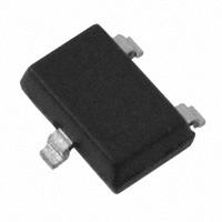
3-pin SOT23-W
2 mm × 3 mm × 1 mm
(suffix LH)
Not to scale
Continued on the next page…
Approximate footprint
Functional Block Diagram
CBYPASS
VCC
Chip Reference
Currents
Amp
To all subcircuits
Filter
Dynamic Offset
Cancellation
V+
Out
Hall Drive Circuit
Gain
Gain Temperature
Coefficient
Trim Control
GND
A1386-DS, Rev. 5
Offset
VOUT
�5 V Field-Programmable Linear Hall Effect Sensor IC with 3 V Supply
Functionality Analog Output, and Miniature Package Options
A1386
Description (continued)
2.7 to 5.5 V supply operating region. Both the quiescent voltage
output and magnetic sensitivity are user adjustable. The quiescent
voltage output can be set to approximately 50% of the supply voltage,
and the sensitivity adjusted between 1.90 and 3.50 mV/G for VCC
= 5 V. The sensitivity temperature coefficient is programmed at the
factory, at 0.13%/°C nominal, to compensate for Neodymium-style
magnets. The features of this linear device make it ideal for the high
accuracy requirements of automotive and industrial applications.
Performance is guaranteed over an extended temperature range,
–40°C to 150°C.
Each device contains a BiCMOS monolithic circuit that integrates
a Hall element, temperature-compensating circuitry to reduce the
intrinsic sensitivity drift of the Hall element, a small-signal high-gain
amplifier, a clamped low-impedance output stage, and a proprietary
dynamic offset cancellation technique.
The A1386 device is provided in a 3-pin ultramini single-in-line
package (UA suffix), and a 3-pin surface mount SOT-23W package
(LH suffix). Both packages are lead (Pb) free, with 100% matte tin
leadframe plating.
Selection Guide
Part Number
Packing*
A1386LLHLT-T
Tape and reel, 3000 pieces/reel
A1386LUA-T
Bulk bag, 500 pieces/bag
*Contact Allegro for additional packing options.
Absolute Maximum Ratings
Characteristic
TA
(°C)
Package
Surface mount
Through hole
Symbol
–40 to 150
Notes
Rating
Units
Forward Supply Voltage
VCC
8
V
Reverse Supply Voltage
VRCC
–0.1
V
Forward Output Voltage
VOUT
28
V
Reverse Output Voltage
VROUT
–0.1
V
Output Source Current
IOUT(SOURCE)
VOUT to GND
8
mA
IOUT(SINK)
VCC to VOUT
2
mA
Output Sink Current
Operating Ambient Temperature
TA
–40 to 150
ºC
Storage Temperature
Tstg
–65 to 165
ºC
TJ(max)
165
ºC
Maximum Junction Temperature
Range L
Pin-out Diagrams
LH Package
UA Package
3
1
Terminal List Table
Number
2
1
2
3
LH
UA
1
1
Name
VCC
Description
Input power supply; use bypass capacitor to connect to ground
3
2
GND
Ground
2
3
VOUT
Output signal
Allegro MicroSystems, LLC
115 Northeast Cutoff
Worcester, Massachusetts 01615-0036 U.S.A.
1.508.853.5000; www.allegromicro.com
2
�A1386
5 V Field-Programmable Linear Hall Effect Sensor IC with 3 V Supply
Functionality Analog Output, and Miniature Package Options
OPERATING CHARACTERISTICS, valid over full operating temperature range, TA; CBYPASS= 0.1 µF, unless otherwise specified
Characteristic
Symbol
Test Conditions
Min.
Typ.
Max.
Units1
VCC(NORM)
4.5
–
5.5
V
VCC(LOWPWR)
2.8
–
3.2
V
Electrical Characteristics
Supply Voltage
Supply Voltage Turn On Time
Operation Mode Threshold
Voltage2
tVCC
–
–
10
ms
VCC(LOWPWR) → VCC(NORM)
–
4.1
–
V
VCC(NORM) → VCC(LOWPWR)
–
3.7
–
V
TA = 25°C, ICC = 11 mA
6
8.3
–
V
VCC = VCC(NORM) , RL(PULLDWN) = 10 kΩ
–
6.4
8
mA
VCC = VCC(LOWPWR) , RL(PULLDWN) = 10 kΩ
–
–
4
mA
VCC = VCC(NORM), TA = 25°C, CBYPASS = open,
CL (of test probe) = 4.7 nF
–
30
–
µs
VCC = VCC(LOWPWR), TA = 25°C, CBYPASS = open,
CL (of test probe) = 4.7 nF
–
50
–
µs
Small signal –3 dB, 100 G(p-p), magnetic input signal
–
20
–
kHz
TA = 25°C
–
200
–
kHz
VCC = 5 V, TA = 25°C, B = 750 G,
Sens = 3.3 mV/G, RL(PULLDWN) = 10 kΩ
4.39
4.5
4.58
V
VCC = 3 V, TA = 25°C, B = 750 G,
Sens = 3.3 mV/G, RL(PULLDWN) = 10 kΩ
2.62
2.7
2.78
V
VCC = 5 V, TA = 25°C, B = –750 G,
Sens = 3.3 mV/G, RL(PULLDWN) = 10 kΩ
0.39
0.5
0.58
V
VCC = 3 V, TA = 25°C, B = –750 G,
Sens = 3.3 mV/G, RL(PULLDWN) = 10 kΩ
0.19
0.3
0.37
V
VCC = VCC(NORM), TA = 25°C, CL = 4.7 nF,
Sens = 3.3 mV/G, no external filter
–
18
–
mV
VCC = VCC(LOWPWR), TA = 25°C, CL = 4.7 nF,
Sens = 1.75 mV/G, no external filter
–
18
–
mV
–
|BPOS1| and |BNEG2| > |BNEG1|. Then:
SensBx =
LinERR = max( LinERRPOS , LinERRNEG )
.
(11)
Symmetry Sensitivity Error The magnetic sensitivity of the
A1386 device is constant for any two applied magnetic fields of
equal magnitudes and opposite polarities.
Symmetry error, SymERR (%), is measured and defined as:
SensBPOS
SymERR = 1–
SensBNEG
× 100%
,
(12)
where SensBx is as defined in equation 10, and BPOS and BNEG
are positive and negative magnetic fields such that |BPOS| = |BNEG|.
Ratiometry Error The A1386 device features a ratiometric
output. This means that the quiescent voltage output, VOUT(Q) ,
magnetic sensitivity, Sens, and clamp voltages, VCLP(HIGH) and
VCLP(LOW), are proportional to the supply voltage, VCC. In other
words, when the supply voltage increases or decreases by a
certain percentage, each characteristic also increases or decreases
by the same percentage. Error is the difference between the
measured change in the supply voltage relative to 5 V, and the
measured change in each characteristic.
The ratiometric error in quiescent voltage output, RatERRVOUT(Q)
(%), for a given supply voltage, VCC, is defined as:
VOUT(Q)(VCC) / VOUT(Q)(5V)
× 100% . (13)
RatERRVOUT(Q) = 1–
VCC / 5 V
The ratiometric error in magnetic sensitivity, RatERRSens (%), for
a given supply voltage, VCC, is defined as:
Sens(VCC) / Sens(5V)
× 100%
RatERRSens = 1–
VCC / 5 V
.
(14)
The ratiometric error in the clamp voltages, RatERRCLP (%), for a
given supply voltage, VCC, is defined as:
VCLP(VCC) / VCLP(5V)
× 100%
RatERRCLP = 1–
VCC / 5 V
.
(15)
where VCLP is either VCLP(HIGH) or VCLP(LOW).
Allegro MicroSystems, LLC
115 Northeast Cutoff
Worcester, Massachusetts 01615-0036 U.S.A.
1.508.853.5000; www.allegromicro.com
9
�A1386
5 V Field-Programmable Linear Hall Effect Sensor IC with 3 V Supply
Functionality Analog Output, and Miniature Package Options
Typical Application Drawing
V+
VCC
VOUT
CL
CBYPASS
GND
Chopper Stabilization Technique
When using Hall-effect technology, a limiting factor for
switchpoint accuracy is the small signal voltage developed across
the Hall element. This voltage is disproportionally small relative
to the offset that can be produced at the output of the Hall element. This makes it difficult to process the signal while maintaining an accurate, reliable output over the specified operating
temperature and voltage ranges. Chopper stabilization is a unique
approach used to minimize Hall offset on the chip. The Allegro
technique, namely Dynamic Quadrature Offset Cancellation,
removes key sources of the output drift induced by thermal and
mechanical stresses. This offset reduction technique is based on
a signal modulation-demodulation process. The undesired offset
signal is separated from the magnetic field-induced signal in the
frequency domain, through modulation. The subsequent demodulation acts as a modulation process for the offset, causing the
magnetic field-induced signal to recover its original spectrum at
base band, while the DC offset becomes a high-frequency signal.
The magnetic-sourced signal then can pass through a low-pass
filter, while the modulated DC offset is suppressed. The chopper
stabilization technique uses a 200 kHz high frequency clock. For
the demodulation process, a sample and hold technique is used,
where the sampling is performed at twice the chopper frequency
(400 kHz). This high-frequency operation allows a greater
sampling rate, which results in higher accuracy and faster signalprocessing capability. This approach desensitizes the chip to the
effects of thermal and mechanical stresses, and produces devices
that have extremely stable quiescent Hall output voltages and
Precise recoverability after temperature cycling. This technique
is made possible through the use of a BiCMOS process, which
allows the use of low-offset, low-noise amplifiers in combination
with high-density logic integration and sample-and-hold circuits.
Regulator
Clock/Logic
Amp
Sample and
Hold
Hall Element
Low-Pass
Filter
Chopper Stabilization Technique
Allegro MicroSystems, LLC
115 Northeast Cutoff
Worcester, Massachusetts 01615-0036 U.S.A.
1.508.853.5000; www.allegromicro.com
10
�5 V Field-Programmable Linear Hall Effect Sensor IC with 3 V Supply
Functionality Analog Output, and Miniature Package Options
A1386
Programming Guidelines
Overview
Definition of Terms
Programming is accomplished by sending a series of input voltage pulses serially through the VOUT pin of the device. A unique
combination of different voltage level pulses controls the internal
programming logic of the device to select a target programmable
parameter and change its value. There are two programming
pulses, referred to as a high voltage pulse, VPH, consisting of a
VP(LOW) –VP(HIGH) –VP(LOW) sequence and a mid voltage pulse,
VPM, consisting of a VP(LOW) –VP(MID) –VP(LOW) sequence.
Register. The section of the programming logic that controls the
choice of programmable modes and parameters.
The A1386 features Try mode, Blow mode, and Lock mode:
• In Try mode, the value of a single programmable parameter may
be set and measured. The parameter value is stored temporarily,
and resets after cycling the supply voltage. Note that other
parameters cannot be accessed simultaneously in this mode.
• In Blow mode, the value of a single programmable parameter
may be permanently set by blowing solid-state fuses internal to
the device. Additional parameters may be blown sequentially.
• In Lock mode, a device-level fuse is blown, blocking the further
programming of all parameters.
The programming sequence is designed to help prevent the
device from being programmed accidentally; for example, as a
result of noise on the supply line.
Although any programmable variable power supply can be used
to generate the pulse waveforms, Allegro highly recommends
using the Allegro Sensor IC Evaluation Kit, available on the
Allegro website On-line Store. The manual for that kit is available for download free of charge, and provides additional information on programming these devices.
Bit Field. The internal fuses unique to each register, represented
as a binary number. Incrementing the bit field of a particular
register causes its programmable parameter to change, based on
the internal programming logic.
Key. A series of VPM voltage pulses used to select a register, with
a value expressed as the decimal equivalent of the binary value.
The LSB of a register is denoted as key 1, or bit 0.
Code. The number used to identify the combination of fuses
activated in a bit field, expressed as the decimal equivalent of the
binary value. The LSB of a bit field is denoted as code 1, or bit 0.
Addressing. Incrementing the bit field code of a selected register
by serially applying a pulse train through the VOUT pin of the
device. Each parameter can be measured during the addressing
process, but the internal fuses must be blown before the programming code (and parameter value) becomes permanent.
Fuse Blowing. Applying a VPH voltage pulse of sufficient duration at the VP(HIGH) level to permanently set an addressed bit by
blowing a fuse internal to the device. Once a bit (fuse) has been
blown, it cannot be reset.
Blow Pulse. A VPH voltage pulse of sufficient duration at the
VP(HIGH) level to blow the addressed fuse.
Cycling the Supply. Powering-down, and then powering-up the
supply voltage. Cycling the supply is used to clear the programming settings in Try mode.
Programming Pulse Requirements, Protocol at TA = 25°C
Characteristic
Symbol
Notes
Min.
Typ.
-
-
5.5
V
14
15
16
V
26
27
28
V
Minimum supply current required to ensure proper fuse blowing. In addition, a minimum capacitance, CBLOW = 0.1 µF, must be connected between the VOUT and
GND pins during programming to provide the current necessary for fuse blowing.
300
-
-
mA
tOFF(HIGH)
Duration at VP(LOW) level following a VP(HIGH) level.
30
-
-
µs
tOFF(MID)
Duration at VP(LOW) level following a VP(MID) level.
5
-
-
µs
VP(LOW)
Programming Voltage
VP(MID)
Measured at the VOUT pin.
VP(HIGH)
Programming Current
Pulse Width
IP
Max. Units
tACTIVE(HIGH)
Duration of VP(HIGH) level for VPH pulses during key/code selection.
30
-
-
µs
tACTIVE(MID)
Duration of VP(MID) level for VPH pulses during key/code selection.
15
-
-
µs
tBLOW
Duration at VP(HIGH) level for fuse blowing.
30
-
-
µs
Pulse Rise Time
tPr
Rise time required for transitions from VP(LOW) to either VP(MID) or VP(HIGH).
1
-
100
µs
Pulse Fall Time
tPf
Fall time required for transitions from VP(HIGH) to either VP(MID) to VP(LOW).
1
-
100
µs
Allegro MicroSystems, LLC
115 Northeast Cutoff
Worcester, Massachusetts 01615-0036 U.S.A.
1.508.853.5000; www.allegromicro.com
11
�5 V Field-Programmable Linear Hall Effect Sensor IC with 3 V Supply
Functionality Analog Output, and Miniature Package Options
A1386
Programming Procedures
Parameter Selection
Each programmable parameter can be accessed through a specific
register. To select a register, a sequence of voltage pulses consisting of a VPH pulse, a series of VPM pulses, and a VPH pulse
(with no VCC supply interruptions) must be applied serially to
the VOUT pin. The number of VPM pulses is called the key, and
uniquely identifies each register. The pulse train used for selection of the first register, key 1, is shown in figure 4.
The A1386 has two registers that select among the three programmable parameters:
• Register 1:
Sensitivity, Sens
• Register 2:
Quiescent voltage output, VOUT(Q)
Overall device locking, LOCK
When addressing the bit field, the number of VPM pulses is represented by a decimal number called a code. Addressing activates
the corresponding fuse locations in the given bit field by incrementing the binary value of an internal DAC. The value of the bit
field (and code) increments by one with the falling edge of each
VPM pulse, up to the maximum possible code (see the Programming Logic table). As the value of the bit field code increases, the
value of the programmable parameter changes.
Measurements can be taken after each pulse to determine if the
desired result for the programmable parameter has been reached.
Cycling the supply voltage resets all the locations in the bit field
that have unblown fuses to their initial states.
Fuse Blowing
VP(HIGH)
VP(HIGH)
VP(MID)
VP(MID)
VP(LOW)
Code 2n – 1
V+
Code 2n – 2
V+
Code 2
After a programmable parameter has been selected, a VPH pulse
transitions the programming logic into the bit field addressing state. Applying a series of VPM pulses to the VOUT pin of
the device, as shown in figure 5, increments the bit field of the
selected parameter.
Code 1
Bit Field Addressing
After the required code is found for a given parameter, its value
can be set permanently by blowing individual fuses in the appropriate register bit field. Blowing is accomplished by applying
a VPH pulse, called a blow pulse, of sufficient duration at the
VP(HIGH) level to permanently set an addressed bit by blowing a
fuse internal to the device. Due to power requirements, the fuse
for each bit in the bit field must be blown individually. To accomplish this, the code representing the desired parameter value
VP(LOW)
tLOW
0
tACTIVE
Figure 4. Parameter selection pulse train. This shows the sequence for selecting the register corresponding to key 1, indicated by a single VPM pulse.
0
Figure 5. Bit field addressing pulse train. Addressing the bit field by
incrementing the code causes the programmable parameter value to
change. The number of bits available for a given programming code, n,
varies among parameters; for example, the bit field for VOUT(Q) has 6 bits
available, which allows 63 separate codes to be used.
Allegro MicroSystems, LLC
115 Northeast Cutoff
Worcester, Massachusetts 01615-0036 U.S.A.
1.508.853.5000; www.allegromicro.com
12
�5 V Field-Programmable Linear Hall Effect Sensor IC with 3 V Supply
Functionality Analog Output, and Miniature Package Options
A1386
must be translated to a binary number. For example, as shown
in figure 6, decimal code 5 is equivalent to the binary number
101. Therefore bit 2 (code 4) must be addressed and blown, the
device power supply cycled, and then bit 0 (code 1) addressed
and blown. An appropriate sequence for blowing code 5 is shown
in figure 7. The order of blowing bits, however, is not important.
Blowing bit 0 first, and then bit 2 is acceptable.
Locking the Device
Note: After blowing, the programming is not reversible, even
after cycling the supply power. Although a register bit field fuse
cannot be reset after it is blown, additional bits within the same
register can be blown at any time until the device is locked. For
example, if bit 1 (binary 10) has been blown, it is still possible to
blow bit 0. The end result would be binary 11 (decimal code 3).
The additional guidelines in this section should be followed to
ensure the proper behavior of these devices:
Bit Field Selection
Address Code Format
(Decimal Equivalent)
Code 5
Code in Binary
(Binary)
1 0 1
Fuse Blowing
Target Bits
Bit 2
Fuse Blowing
Address Code Format
After the desired code for each parameter is programmed, the
device can be locked to prevent further programming of any
parameters.
Additional Guidelines
• A 0.1 µF blowing capacitor, CBLOW, must be mounted between
the VOUT pin and the GND pin during programming, to ensure
enough current is available to blow fuses.
• The CBLOW blowing capacitor must be replaced in the final
application with a suitable CL. (The maximum load capacitance
is 10 nF for proper operation.)
• The power supply used for programming must be capable of
delivering at least 26 V and 300 mA.
• Be careful to observe the tLOW delay time before powering
down the device after blowing each bit.
Bit 0
• The following programming order is recommended:
Code 4
Code 1
(Decimal Equivalents)
1. Sens
2. VOUT(Q)
3. LOCK (only after all other parameters have been programmed and validated, because this prevents any further
programming of the device)
Figure 6. Example of code 5 broken into its binary components, which are
code 4 and code 1.
V+
VP(HIGH)
VP(MID)
VP(LOW)
Register
Selection
(Key 1)
0
VCC = 0 V
Addressing
(Code 4)
Register
Selection
(Key 1)
Blow
(Code 4 in
Key 1)
tBLOW
VCC = 0 V
Blow
(Code 1 in
Key 1)
Addressing
(Code 1)
VCC = 0 V
Programming of Code 5 in Key 1
Figure 7. Example of programming pulses applied to the VOUT pin that
result in permanent parameter settings. In this example, the register
corresponding to key 1 is selected and code 5 is addressed and blown.
Allegro MicroSystems, LLC
115 Northeast Cutoff
Worcester, Massachusetts 01615-0036 U.S.A.
1.508.853.5000; www.allegromicro.com
13
�A1386
5 V Field-Programmable Linear Hall Effect Sensor IC with 3 V Supply
Functionality Analog Output, and Miniature Package Options
Programming Modes
Try Mode
Try mode allows a single programmable parameter to be tested
without permanently setting its value. Multiple parameters cannot
be tested simultaneously in this mode. After powering the VCC
supply, select the desired parameter register and address its bit
field. When addressing the bit field, each VPM pulse increments
the value of the parameter register, up to the maximum possible
code (see Programming Logic table). The addressed parameter
value remains stored in the device even after the programming
drive voltage is removed from the VOUT pin, allowing the value
to be measured. Note that for accurate time measurements, the
blow capacitor, CBLOW, should be removed during output voltage
measurement.
It is not possible to decrement the value of the register without
resetting the parameter bit field. To reset the bit field, and thus the
value of the programmable parameter, cycle the supply (VCC) voltage.
Blow Mode
After the required value of the programmable parameter is found
using Try mode, its corresponding code should be blown to make
its value permanent. To do this, select the required parameter
register, and address and blow each required bit separately (as
described in the Fuse Blowing section). The supply must be
cycled between blowing each bit of a given code. After a bit is
blown, cycling the supply will not reset its value.
Lock Mode
To lock the device, address the LOCK bit and apply a blow pulse
with CBLOW in place. After locking the device, no future programming of any parameter is possible.
Allegro MicroSystems, LLC
115 Northeast Cutoff
Worcester, Massachusetts 01615-0036 U.S.A.
1.508.853.5000; www.allegromicro.com
14
�5 V Field-Programmable Linear Hall Effect Sensor IC with 3 V Supply
Functionality Analog Output, and Miniature Package Options
A1386
Programming State Machine
Power-Up
VPM
Initial
VPH
VPH
Parameter Selection
VPM
VPM
Sens
VPM
VOUT(Q),
LOCK
VPH
Bit Field Addressing
VPM
1
VPM
VPM
2
3
VPM
2n – 1
n = total
bits in
register
VPM
VPH
VPM = VP(LOW) , VP(MID) , VP(LOW)
VPH = VP(LOW) , VP(HIGH) , VP(LOW)
Fuse Blowing
User Power-Down
Required
Initial State After system power-up, the programming logic is
reset to a known state. This is referred to as the Initial state. All
the bit field locations that have intact fuses are set to logic 0.
While in the Initial state, any VPM pulses on the VOUT pin are
ignored. To enter the Parameter Selection state, apply one VPH
pulse on the VOUT pin.
Parameter Selection State This state allows the selection of the
Bit Field Addressing State This state allows the selection of the
individual bit fields to be programmed in the selected parameter
register (see Programming Logic table). To leave this state, either
cycle device power or blow the fuses for the selected code. Note
that merely addressing the bit field does not permanently set
the value of the selected programming parameter; fuses must be
blown to do so.
parameter register containing the bit fields to be programmed. To
select a parameter register, increment through the keys by applying VPM pulses on the VOUT pin. Register keys select among the
following programming parameters:
• 1 pulse - Sens
VPH pulse on the VOUT pin. Power to the device should then be
• 2 pulses - VOUT(Q) and LOCK
cycled before additional programming is attempted. Note: Each
To enter the Bit Field Addressing state, apply one VPH pulse on
the VOUT pin.
the Fuse Blowing section).
Fuse Blowing State To blow an addressed bit field, apply a
bit representing a decimal code must be blown individually (see
Allegro MicroSystems, LLC
115 Northeast Cutoff
Worcester, Massachusetts 01615-0036 U.S.A.
1.508.853.5000; www.allegromicro.com
15
�5 V Field-Programmable Linear Hall Effect Sensor IC with 3 V Supply
Functionality Analog Output, and Miniature Package Options
A1386
Programming Logic Table
Programmable
Parameter
(Register Key)
Sens
(1)
VOUT(Q) , LOCK
(2)
Bit Field Address
Binary Format
[MSB → LSB]
Decimal Equivalent
Code
000000
0
Description
Initial value (Sensinit)
111111
63
Maximum value of sensitivity (Sens) in range
000000
0
Initial value (VOUT(Q)init)
001111
15
Maximum value of quiescent voltage output
(VOUT(Q)) in range; B = 0 G
010000
16
Minimum value of quiescent voltage output
(VOUT(Q)) in range; B = 0 G
100000
32
LOCK bit, enables permanent locking of all programming bit fields in the device
QVO Voltage ,VOUT(Q)
QVO_Max
QVO_Init
QVO_Init -1 Step
QVO_Min
0
15
16
31
Codes (Decimal)
Allegro MicroSystems, LLC
115 Northeast Cutoff
Worcester, Massachusetts 01615-0036 U.S.A.
1.508.853.5000; www.allegromicro.com
16
�5 V Field-Programmable Linear Hall Effect Sensor IC with 3 V Supply
Functionality Analog Output, and Miniature Package Options
A1386
Package LH, 3 Pin; (SOT-23W)
+0.12
2.98 –0.08
1.49 D
4°±4°
3
A
+0.020
0.180–0.053
0.96 D
+0.10
2.90 –0.20
+0.19
1.91 –0.06
2.40
0.70
D
0.25 MIN
1.00
2
1
0.55 REF
0.25 BSC
0.95
Seating Plane
Gauge Plane
8X 10° REF
B
PCB Layout Reference View
Branded Face
1.00 ±0.13
0.95 BSC
+0.10
0.05 –0.05
0.40 ±0.10
For Reference Only; not for tooling use (reference dwg. 802840)
Dimensions in millimeters
Dimensions exclusive of mold flash, gate burrs, and dambar protrusions
Exact case and lead configuration at supplier discretion within limits shown
A
Active Area Depth, 0.28 mm REF
B
Reference land pattern layout
All pads a minimum of 0.20 mm from all adjacent pads; adjust as necessary
to meet application process requirements and PCB layout tolerances
C
Branding scale and appearance at supplier discretion
D
Hall element, not to scale
NNT
1
C
Standard Branding Reference View
N = Last two digits of device part number
T = Temperature code
Allegro MicroSystems, LLC
115 Northeast Cutoff
Worcester, Massachusetts 01615-0036 U.S.A.
1.508.853.5000; www.allegromicro.com
17
�5 V Field-Programmable Linear Hall Effect Sensor IC with 3 V Supply
Functionality Analog Output, and Miniature Package Options
A1386
Package UA, 3-Pin SIP
+0.08
4.09 –0.05
45°
B
C
E
2.04
1.52 ±0.05
1.44 E
+0.08
3.02 –0.05
Mold Ejector
Pin Indent
2X10°
E
45°
1
D Standard Branding Reference View
A
1.02
MAX
0.51
REF
Branded
Face
= Supplier emblem
N = Last two digits of device part number
T = Temperature code
0.79 REF
1
2
3
+0.03
0.41 –0.06
14.99 ±0.25
+0.05
0.43 –0.07
NNT
For Reference Only; not for tooling use (reference DWG-9013)
Dimensions in millimeters
Dimensions exclusive of mold flash, gate burrs, and dambar protrusions
Exact case and lead configuration at supplier discretion within limits shown
A
Dambar removal protrusion (6X)
B
Gate and tie bar burr area
C
Active Area Depth, 0.50 mm REF
D
Branding scale and appearance at supplier discretion
E
Hall element, not to scale
1.27 NOM
Please note that there are changes to the existing UA package drawing pending.
Please contact the Allegro Marketing department for additional information.
Allegro MicroSystems, LLC
115 Northeast Cutoff
Worcester, Massachusetts 01615-0036 U.S.A.
1.508.853.5000; www.allegromicro.com
18
�A1386
5 V Field-Programmable Linear Hall Effect Sensor IC with 3 V Supply
Functionality Analog Output, and Miniature Package Options
Copyright ©2009-2015, Allegro MicroSystems, LLC
Allegro MicroSystems, LLC reserves the right to make, from time to time, such departures from the detail specifications as may be required to
permit improvements in the performance, reliability, or manufacturability of its products. Before placing an order, the user is cautioned to verify that
the information being relied upon is current.
Allegro’s products are not to be used in any devices or systems, including but not limited to life support devices or systems, in which a failure of
Allegro’s product can reasonably be expected to cause bodily harm.
The information included herein is believed to be accurate and reliable. However, Allegro MicroSystems, LLC assumes no responsibility for its
use; nor for any infringement of patents or other rights of third parties which may result from its use.
For the latest version of this document, visit our website:
www.allegromicro.com
Allegro MicroSystems, LLC
115 Northeast Cutoff
Worcester, Massachusetts 01615-0036 U.S.A.
1.508.853.5000; www.allegromicro.com
19
�


 工商网监
湘ICP备2023018690号
工商网监
湘ICP备2023018690号
