A3932
Three-Phase Power MOSFET Controller
Discontinued Product
This part is no longer in production. The part should not be purchased
for new design applications. Samples are no longer available.
Date of status change: June 1, 2016
Recommended Substitutions:
For existing customer transition, and for new customers or new applications, refer to A3938SLDTR-T.
NOTE: For detailed information on purchasing options, contact your
local Allegro field applications engineer or sales representative.
Allegro MicroSystems, LLC reserves the right to make, from time to time, revisions to the anticipated product life cycle plan
for a product to accommodate changes in production capabilities, alternative product availabilities, or market demand. The
information included herein is believed to be accurate and reliable. However, Allegro MicroSystems, LLC assumes no responsibility for its use; nor for any infringements of patents or other rights of third parties which may result from its use.
�A3932
Three-Phase Power MOSFET Controller
Features and Benefits
▪ Drives wide range of N-channel MOSFETs
▪ Synchronous rectification
▪ Power MOSFET protection
▪ Adjustable dead time for cross-conduction protection
▪ 100% duty cycle operation
▪ Selectable fast or slow current-decay modes
▪ Internal PWM peak current control
▪ High-current gate drive
▪ Motor lead short-to-ground protection
▪ Internal 5 V regulator
▪ Brake input
▪ PWM torque-control input
▪ Fault-diagnostic output
▪ Tachometer output
▪ Thermal shutdown
▪ Undervoltage protection
Description
The A3932 is a three-phase MOSFET controller for use with
bipolar brushless DC motors. Its high gate-current drive
capability allows driving a wide range of N-channel power
MOSFETs and can support motor supply voltages to 50 V.
Bootstrapped high-side drive blocks provide the floating
positive supplies for the gate drive and minimize the component
count normally required. The high-side circuitry also employs a
unique FET monitoring circuit that ensures the gate voltages are
at the proper levels before turn-on and during the ON cycle.
Internal fixed off-time PWM current-control circuitry can be
used to regulate the maximum load current to a desired value.
The peak load-current limit is set by the user’s selection of
an input reference voltage and external sensing resistor. The
fixed off-time pulse duration is set by a user-selected external
RC timing network. For added flexibility, the PWM input can
be used to provide speed/torque control, allowing the internal
current control circuit to set the maximum current limit.
Optional synchronous rectification is included. This feature will
short out the current path through the power MOSFET reverse
body diodes during the PWM off-cycle current decay. This can
minimize power dissipation in the power MOSFET, eliminate
the need for external power clamp diodes, and potentially allow
more economical choices for the MOSFET application.
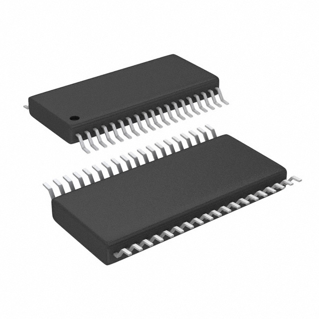
Packages
38-pin TSSOP (suffix LD)
The A3932 includes the commutation logic for Hall sensors
configured for 120 degree spacing. Power MOSFET protection
features include bootstrap capacitor charging current monitor,
undervoltage monitor, motor-lead short-to-ground, and thermal
shutdown.
The ‘–S–’ part-number suffix indicates an operating temperature
range of -20°C to +85°C. The ‘–LD–’ suffix indicates a 38‑lead
TSSOP package. The initial ‘–TR–’ variant suffix indicates
tape and reel packing. The ‘–T’ final variant suffix indicates
lead (Pb) free composition, with 100% matte tin leadframe
plating.
Not to scale
26301.101I
�A3932
Three-Phase Power MOSFET Controller
Selection Guide
Part Number
A3932SLDTR-T
Packing
4000 pieces per reel
Absolute Maximum Ratings
Characteristic
Symbol
Notes
Rating
Units
50
V
Supply Voltage
VBB
Peak Regulator Voltage
VREG
15
V
VIN
–0.3 to VLCAP + 0.3
V
VSENSE
–5 to 1.5
V
Logic Input Voltage Range
Sense Voltage Range
Output Voltage Range
SA, SB, SC Pins
GHA, GHB, GHC Pins
CA, CB, CC Pins
Operating Ambient Temperature
V
TA
Range S
–5 to 50
V
–5 to VBB + 17
V
VSx + 17
V
–20 to 85
ºC
Junction Temperature
TJ
150
ºC
Storage Temperature
Tstg
–55 to 150
ºC
Allegro MicroSystems, LLC
115 Northeast Cutoff
Worcester, Massachusetts 01615-0036 U.S.A.
1.508.853.5000; www.allegromicro.com
2
�A3932
Three-Phase Power MOSFET Controller
Pin-Out Diagram
38-pin TSSOP (suffix LD)
RESET
1
38
NC
GLC
2
37
NC
SC
3
36
PGND
NC
4
35
AGND
NC
5
34
DEAD
GHC
6
33
REF
CC
7
32
SENSE
GLB
8
31
RC
SB
9
30
PWM
GHB
10
29
TACH
CB
11
28
SR
GLA
12
27
BRAKE
SA
13
26
DIR
GHA
14
25
H2
CA
15
24
H3
VREG
16
23
NC
LCAP
17
22
H1
NC
18
21
VBB
FAULT
19
20
MODE
CONTROL
LOGIC
FAULT
Allegro MicroSystems, LLC
115 Northeast Cutoff
Worcester, Massachusetts 01615-0036 U.S.A.
1.508.853.5000; www.allegromicro.com
3
�A3932
Three-Phase Power MOSFET Controller
Functional Block Diagram
NOTE — For 12 V applications, VBB is shorted to VREG.
The VREG absolute maximum rating (15 V) must not be
exceeded.
Allegro MicroSystems, LLC
115 Northeast Cutoff
Worcester, Massachusetts 01615-0036 U.S.A.
1.508.853.5000; www.allegromicro.com
4
�A3932
Three-Phase Power MOSFET Controller
ELECTRICAL CHARACTERISTICS: unless otherwise noted at TA = 25°C; VBB = 18 V to 50 V; CLCAP,
Cboot = 0.1 µF; CREG = 10 µF; Cload = 3300 pF; fPWM = 22.5 kHz Square Wave; Two Phases Active.
Limits
Parameter
Symbol
Conditions
Min
Typ
Max
Units
–
–
8.0
mA
Supply Current
Quiescent Current
IBB
Reference Voltage
VLCAP
ILCAP = -3 mA
4.75
5.0
5.25
V
Output Voltage
VREG
VBB = VREG ≤15 V, IREG = -10 mA
10.8
–
13.2
V
18 V ≤ VBB ≤ 50 V, IREG = -10 mA
12.4
13
13.6
V
–
VBB - 2.5
–
V
–
25
–
mV
RESET high, coast mode, stopped
VBB = 13.2 V to 18 V, IREG = -10 mA
Output Voltage Regulation
ΔVREG(ΔIREG) IREG = -1 to -30 mA, coast
ΔVREG(ΔVBB)
IREG = -10 mA, coast
–
40
–
mV
VIH
All inputs except SR
2.0
–
–
V
SR input only
3.0
–
–
V
All inputs except SR
–
–
0.8
V
SR input only
–
–
1.8
V
Digital Logic Levels
Logic Input Voltage
VIL
Logic Input Current
IIH
VIH = 2 V
-30
–
-90
µA
IIL
VIL = 0.8 V
-50
–
-130
µA
–
V
Gate Drive
Low-Side Output Voltage
VGLxH
IGLx = 0
High-Side Output Voltage
VGHxH
IGHx = 0
Pulldown Switch Resistance
rDS(on)
Pullup Switch Resistance
rDS(on)
VREG - 0.8 VREG - 0.5
10.4
11.6
12.8
V
IGLx = 50 mA
–
4.0
–
Ω
IGHx = -50 mA
–
14
–
Ω
Low-Side Output
Switching Time
trGLx
10% to 90%, with Cload
–
120
–
ns
tfGLx
90% to 10%, with Cload
–
60
–
ns
High-Side Output
Switching Time
trGHx
10% to 90%, with Cload
–
120
–
ns
tfGHx
90% to 10%, with Cload
–
60
–
ns
tpr
GHx, GLx rising, Cload = 0
–
220
–
ns
tpf
GHx, GLx falling, Cload = 0
–
110
–
ns
Propagation Delay Time
(PWM to gate output)
Maximum Dead Time
tdead
GHx to GLx, VDEAD = 0 V, Cload = 0
3.5
5.6
7.6
µs
Minimum Dead Time
tdead
GLx to GHx, IDEAD = 780 µA, Cload = 0
50
100
150
ns
NOTES: 1. Typical Data is for design information only.
2. Negative current is defined as coming out of (sourcing) the specified device terminal.
Continued —
Allegro MicroSystems, LLC
115 Northeast Cutoff
Worcester, Massachusetts 01615-0036 U.S.A.
1.508.853.5000; www.allegromicro.com
5
�A3932
Three-Phase Power MOSFET Controller
ELECTRICAL CHARACTERISTICS: unless otherwise noted at TA = 25°C; VBB = 18 V to 50 V; CLCAP,
Cboot = 0.1 µF; CREG = 10 µF; Cload = 3300 pF; fPWM = 22.5 kHz Square Wave; Two Phases Active.
Parameter
Symbol
Conditions
Limits
Min
Typ
Max
Units
100
–
–
mA
10.4
11.6
12.8
V
Bootstrap Capacitor
Bootstrap Charge Current
ICx
Bootstrap Output Voltage
VCx
VSx = 0, ICx = 0, VREG = 13 V
Bootstrap Resistance
rCx
ICx = -50 mA
–
9.0
12
Ω
Vio
0 V ≤ VIC ≤ 1.5 V
–
–
±5.0
mV
ISENSE
VIC ≥ 0 V, VID ≤ 1.5 V
–
-25
–
µA
REFERENCE Input Current
IREF
VIC ≥ 0 V, VID ≤ 1.5 V
–
0
–
µA
Blank Time
tblank
RT = 56 kΩ, CT = 470 pF
–
0.91
–
µs
IRC
-0.9
-1.0
-1.1
mA
VRCL
1.0
1.1
1.2
V
VRCH
2.7
3.0
3.3
V
Bootstrap Charge Threshold
ICx
–
-9.0
–
mA
Motor Short-to-Ground Monitor
VDSH
VBB - VSX, high side on
1.3
2.0
2.7
V
Undervoltage Threshold
UVLO
Increasing VREG
9.2
9.7
10.2
V
Decreasing VREG
8.6
9.1
9.6
V
Current Limit Circuitry
Input Offset Voltage
SENSE Input Current
RC Charge Current
RC Voltage Threshold
Protection Circuitry
FAULT Output Voltage
VFAULT
IO = 1 mA
–
–
0.5
V
TACH Output Voltage
VTACH
IO = 1 mA
–
–
0.5
V
TACH Output Pulse Width
tTACH
IO = 1 mA, CTACH = 50 pF
–
0.75
–
µs
Thermal Shutdown Temp.
TJ
–
165
–
°C
Thermal Shutdown Hysteresis
∆TJ
–
10
–
°C
Thermal Resistance
RθJA
Package EQ Four-layer PCB
–
37
–
°C/W
Package LD Four-layer PCB
–
51
–
°C/W
NOTES:
1. Typical Data is for design information only.
2. Negative current is defined as coming out of (sourcing) the specified device terminal.
Allegro MicroSystems, LLC
115 Northeast Cutoff
Worcester, Massachusetts 01615-0036 U.S.A.
1.508.853.5000; www.allegromicro.com
6
�A3932
Three-Phase Power MOSFET Controller
Terminal Descriptions
LD
Name
1
RESET
2
GLC
3
SC
4,5,18,
NC
23,37,38
6
GHC
7
CC
8
GLB
9
SB
10
GHB
11
CB
12
GLA
13
SA
14
GHA
15
CA
16
VREG
17
LCAP
19
FAULT
20
MODE
21
VBB
22
H1
24
H3
25
H2
26
DIR
27
BRAKE
28
SR
29
TACH
30
PWM
31
RC
32
SENSE
33
REF
34
DEAD
35
AGND
36
PGND
RESET — A logic input used to enable the device, internally
pulled up to VLCAP (+5 V). A RESET = 1 will disable the device
and force all gate drivers to 0 V, coasting the motor. A RESET
= 0 allows the gate drive to follow the commutation logic. The
RESET = 1 overrides BRAKE.
GLA/GLB/GLC — Low-side, gate-drive outputs for external
NMOS drivers. External series-gate resistors (as close as possible to the NMOS gate) can be used to control the slew rate
seen at the power-driver gate, thereby controlling the di/dt and
dv/dt of the SA/SB/SC outputs. GLx = 1 (or “high”) means that
the upper half (PMOS) of the driver is turned on and its drain
will source current to the gate of the low-side FET in the external motor-driving bridge. GLx = 0 (or “low”) means that the
lower half (NMOS) of the driver is turned on and its drain will
sink current from the external FET’s gate circuit.
SA/SB/SC — Directly connected to the motor, these terminals
sense the voltages switched across the load. These terminals are
also connected to the negative side of the bootstrap capacitors
and are the negative supply connections for the floating highside drivers.
GHA/GHB/GHC — High-side, gate-drive outputs for external
NMOS drivers. External series-gate resistors can be used to
control the slew rate seen at the power-driver gate, thereby controlling the di/dt and dv/dt of the SA/SB/SC outputs.
GHx = 1 (or “high”) means that the upper half (PMOS) of the
driver is turned on and its drain will source current to the gate of
the high-side FET in the external motor-driving bridge. GHx =
0 (or “low”) means that the lower half (NMOS) of the driver is
turned on and its drain will sink current from the external FET’s
gate circuit.
CA/CB/CC — High-side connections for the bootstrap capacitors, positive supply for high-side gate drivers. The bootstrap
capacitors are charged to approximately VREG when the associated output Sx terminal is low. When the output swings high,
the voltage on this terminal rises with the output to provide the
boosted gate voltage needed for N-channel power MOSFETs.
continued next page
Allegro MicroSystems, LLC
115 Northeast Cutoff
Worcester, Massachusetts 01615-0036 U.S.A.
1.508.853.5000; www.allegromicro.com
7
�A3932
Three-Phase Power MOSFET Controller
Terminal Descriptions (cont’d)
FAULT — Open-drain output to indicate fault condition; FAULT
= 1 (external pull-up) for any of the following:
1 – invalid HALL input code,
2 – undervoltage condition detected at VREG.
3 – thermal shutdown, or
4 – motor lead (SA/SB/SC) shorted to ground.
Except for a short-to-ground fault that only turns off the
high-side drivers, faults will force a coast condition that turns off
all power MOSFETs. Only the short-to-ground fault is latched
but is cleared at each commutation. If the motor has stalled
due to a short-to-ground being detected, toggling the RESET
terminal or repeating a power-up sequence will clear the fault.
Typically pulled up to VLCAP (+5 V) with an external 5.1 kΩ
resistor.
MODE — A logic input to set current-decay method, internally
pulled up to VLCAP (+5 V). When in slow-decay mode (MODE
= 1), only the high-side MOSFET is switched off during a
PWM-off cycle. The fast-decay mode (MODE = 0) switches
both the high-side and low-side MOSFETs.
H1/H2/H3 — Hall-sensor inputs; internally pulled up to VLCAP
(+5 V). Configured for 120° electrical spacing.
DIR — A logic input to reverse rotation, see Commutation Truth
Table. Internally pulled up to VLCAP (+5 V).
BRAKE — An active-low logic input for a braking function.
A BRAKE = 0 will turn on the low-side FETs and turn off the
high-side FETs. This will effectively short-circuit the BEMF in
the windings and brake the motor. The braking torque applied
will depend on the speed. Internally pulled up to VLCAP (+5 V).
RESET = 1 overrides BRAKE and will coast the motor.
SR — Synchronous rectification input. An SR = 0 disables this
feature, forcing current decay through the body diodes of the
power MOSFETs. An SR = 1 will result in appropriate highand low-side gate outputs to switch in response to a PWM-off
command. Internally pulled up to VLCAP (+5 V). See also the
Input Logic table.
TACH — An open-drain digital output whose frequency is proportional to speed of rotation. A pulse appears at every HALL
transition. Typically pulled up to VLCAP (+5 V) with an external
5.1 kΩ resistor.
PWM — Speed control input, internally pulled up to VLCAP
(+5 V). A PWM = 0 turns off selected drivers. A PWM = 1 will
turn on selected drivers as determined by H1/H2/H3 input logic.
Holding PWM = 1 allows speed/torque control solely by the
internal current-limit circuit with the REF analog voltage. See
also the Input Logic table
.
RC — An analog input used to set the fixed off time with an
external resistor (RT) and capacitor (CT). The tblank time is controlled by the value of the external capacitor (see Applications
Information). See Application Information.
SENSE — An analog input to the current-limit comparator.
A voltage representing load current appears on this terminal during on time, when it reaches REF voltage, the comparator trips
and load current decays for the fixed off-time interval. Voltage transients seen at this terminal when the drivers turn on are
ignored for time tblank.
REF — An analog input to the current-limit comparator. Voltage applied here with respect to AGND sets the peak load current.
Ipeak = VREF/RS.
VREG — A regulated 13 V output; supply for low-side gate
drive and bootstrap capacitor charge circuits. It is good practice
to connect a decoupling capacitor from this terminal to AGND,
as close to the device terminals as possible. This terminal should
be shorted to VBB for 12 V applications.
VBB — The A3932 supply voltage. It is good practice to connect a decoupling capacitor from this terminal to AGND, as
close to the device terminals as possible.
LCAP — Connection for 0.1 µF decoupling capacitor for the
internal 5 V reference. This terminal can source no more than
3 mA for the DEAD input, TACH and FAULT outputs.
DEAD — An analog input. A resistor between DEAD and
LCAP is selected to adjust the turn-off to turn-on time. This
delay is needed to prevent shoot-through in the external power
MOSFETs. See Applications Information for details on setting
dead time.
AGND — The low-level (analog) reference point.
PGND — The return for all low-side gate drivers. This should
be connected to the system power ground.
Allegro MicroSystems, LLC
115 Northeast Cutoff
Worcester, Massachusetts 01615-0036 U.S.A.
1.508.853.5000; www.allegromicro.com
8
�A3932
Three-Phase Power MOSFET Controller
Commutation Truth Table
Logic Inputs
H2
H3
H1
1
1
1
0
0
0
1
1
1
0
0
0
0
0
1
1
1
0
0
0
1
1
1
0
DIR
GLA
GLB
1
1
1
1
1
1
0
0
0
0
0
0
0
0
1
1
0
0
1
0
0
0
0
1
0
0
0
0
1
1
0
1
1
0
0
0
1
0
0
0
1
1
1
0
0
0
1
1
Driver Outputs
GLC
GHA
1
1
0
0
0
0
0
0
0
1
1
0
1
0
0
0
0
1
0
0
1
1
0
0
GHB
GHC
0
1
1
0
0
0
0
0
0
0
1
1
0
0
0
1
1
0
1
1
0
0
0
0
Motor Terminals
SA
SB
SC
H
Z
L
L
Z
H
L
Z
H
H
Z
L
Z
H
H
Z
L
L
Z
L
L
Z
H
H
L
L
Z
H
H
Z
H
H
Z
L
L
Z
Input Logic
MODE
PWM
SR
RESET
0
0
1
1
0
0
1
1
X
0
1
0
1
0
1
0
1
X
0
0
0
0
1
1
1
1
X
0
0
0
0
0
0
0
0
1
Operation
PWM chop mode, fast decay, all drivers off
Peak current limit, selected drivers on
PWM chop mode. slow decay, selected low side drivers on
Peak current limit, selected drivers on
PWM chop mode, fast decay with opposite of selected drivers on
Peak current limit, selected drivers on
PWM chop, slow decay with both low-side drivers on
Peak current limit, selected drivers on
All gate drive outputs off, clear fault logic, coast
L = Low (less positive) level
H = High (more positive) level
X = Don’t care
Z = High impedance
1 = Active or true logic condition
0 = Inactive or false logic condition
Allegro MicroSystems, LLC
115 Northeast Cutoff
Worcester, Massachusetts 01615-0036 U.S.A.
1.508.853.5000; www.allegromicro.com
9
�A3932
Three-Phase Power MOSFET Controller
Applications Information
Synchronous Rectification. To reduce power dissipation
in the external MOSFETs, the A3932 control logic turns on the
appropriate low-side and high-side driver during the load-current
recirculation, PWM-off cycle. Synchronous rectification allows
current to flow through the MODE-selected MOSFET, rather
than the body diode, during the decay time. The body diodes of
the SR power MOSFETs will conduct only during the dead time
required at each PWM transition.
Dead Time. It is required to have a dead-time delay between a
high- or low-side turn off and the next turn-on event to prevent
cross conduction. The potential for cross conduction occurs with
synchronous rectification, direction changes, PWM, or after a
bootstrap capacitor charging cycle. The dead time is set by a
resistor (Rdead) between the DEAD terminal and LCAP
(+5 V) and can be set between 100 ns and 5.5 µs.
The following equations are valid for Rdead between 5.6 kΩ
and 470 kΩ. At 25°C,
tdead (nom, ns) = 37 + (11.9 x 10⁻³ x (Rdead + 500))
For predicting worst case, over voltage and temperature
extremes,
tdead (min, ns) = 10 + (6.55 x 10⁻³ x (Rdead + 350))
tdead (max, ns) = 63 + (17.2 x 10⁻³ x (Rdead + 650))
For comparison with IDEAD test currents,
IDEAD = (VLCAP – Vbe)/(Rdead + Rint)
where (nominal values) VLCAP = 5 V, Vbe = 0.7 V at 25°C, and
Rint = 500 Ω.
Rather than use Rdead values near 470 kΩ, set DEAD =
ground (VDEAD = 0 V), which activates an internal (IDEAD =
10 µA) current source.
The choice of power MOSFET and external series gate
resistance determines the selection of the dead-time resistor. The
dead time should be made long enough to cover the variation of
the MOSFET gate capacitance and series gate resistance (both
external and internal to the A3932) tolerances.
Decoupling. The internal reference, VREG, supplies current
for the gate-drive circuit. As the gates are driven high they
will require current from an external capacitor to support the
transients. This capacitor should be placed as close as possible
to the VREG terminal. Its value should be at least 20 times larger
than the bootstrap capacitor.
Additionally, a 0.1 µF (or larger) decoupling capacitor
should be connected between LCAP and AGND as close to the
device terminals as possible.
Protection Circuitry. The A3932 has several protection
features:
1) Bootstrap Circuit. The bootstrap capacitor is charged
whenever a low-side MOSFET is on, Sx output goes low,
and the load current recirculates. This happens constantly
during normal operation. The high-side MOSFET will not be
allowed to turn on before the charging has decayed to less than
approximately 9 mA. No fault will be registered.
When a phase’s high-side driver is on for a long time (100%
duty cycle operation) its charge pump is designed to maintain
VGS > 9 V on the bridge FET if IGHx (the load on the gate driver)
< 10 µA.
2) Hall Invalid. Illegal codes for the HALL inputs (000 or
111) will force a fault and coast the motor. Noisy Hall lines
may cause double TACH pulses and, therefore, code errors that
produce faults. Additional external pullup loading and filtering
may be required depending on the system.
3) VREG Undervoltage. An internal regulator supplies the
low-side gate driver and the bootstrap charge current. It is critical
to ensure that VREG is at the proper level before enabling any of the
outputs. The undervoltage circuit is active during power-up and
will force a motor coast condition (all gate drives, GHx and GLx =
0) until VREG is greater than approximately 9.7 V.
4) Thermal Shutdown. A junction temperature greater than
165°C will signal a fault and coast the motor (all gate drives
LOW). If the junction temperature then falls to less than 155°C
(hysteresis), the fault will be cleared.
5) Motor Lead Shorted to Ground. The A3932 will signal
a fault if a motor lead is shorted to ground. A short to ground
is assumed after a high side is turned on and greater than 2 V is
measured between the drain (VBB) and source (SA/SB/SC) of the
high-side power MOSFET. This fault is cleared at the beginning
of each commutation. If a stalled motor results from a fault, the
fault can only be cleared by toggling the RESET terminal or by a
power-up sequence.
continued next page
Allegro MicroSystems, LLC
115 Northeast Cutoff
Worcester, Massachusetts 01615-0036 U.S.A.
1.508.853.5000; www.allegromicro.com
10
�A3932
Three-Phase Power MOSFET Controller
Applications Information (cont’d)
Current Control. Internal fixed off-time PWM circuitry is
implemented to limit load current to a desired value. When a
high-side and low-side MOSFET are turned on, current will
increase in the motor winding until it reaches a value given by
ITRIP ≈ VREF/RS.
Because the load current does not flow through the sense
resistor during a dynamic brake, care must be taken to ensure
that the power MOSFET’s maximum ratings are not exceeded.
At the trip point, the sense comparator resets the sourceenable latch, turning off the high-side driver. Load inductance
causes the current to recirculate (decay) for the fixed off time.
The current path during recirculation is determined by the
configuration of the MODE and SR inputs.
Low-Voltage Operation. Although VREG can be connected
to VBB for 12 V systems, the VREG maximum rating of 15 V
must be observed including transients. If transients cannot be
adequately controlled, use VREG in the regulator mode (not
connected to VBB). With VBB less than 18 V, the VREG output
voltage level specification may not be met. Note that in this
mode the VREG undervoltage threshold may leave the system
with little headroom if VBB is less than 12 V.
An external resistor (RT) and capacitor (CT), connected
in parallel from the RC terminal to AGND, are used to set the
fixed off-time period (toff = RT x CT). RT should be in the range
of 10 kΩ to 500 kΩ. The toff should be in the range of 10 µs to
50 µs. Larger values for toff can result in audible noise problems.
Torque control can be implemented by varying the REF
input voltage as long as the PWM input stays high. If direct
control of the torque/current is desired by PWM input, a voltage
can be applied to the REF input to set an absolute maximum
current limit.
PWM Blank. The capacitor (CT) also serves as the means to
set the blank time duration. At the end of the PWM off cycle, a
high-side gate selected by the commutation logic will turn on.
At this time, large current transients can occur during the reverse
recovery time (trr) of the intrinsic body diodes of the external
power MOSFETs. To prevent false tripping of the current-sense
comparator, the blank function disables the comparator for a
time
tblank = 1.9 x CT/(0.001 - [2/RT])
The user must ensure that CT is large enough to cover the
current-spike duration.
Braking. The A3932 will dynamically brake by forcing all
low-side MOSFETs on and all high-side MOSFETs off. This
will effectively short-circuit the BEMF and brake the motor.
During braking, the load current can be approximated by:
IBRAKE = VBEMF/RL
RESET = 1 overrides BRAKE and turns all motor bridge
FETs off, coasting the motor.
Driving an H Bridge. The A3932 may be used to drive an
H bridge (e.g., a brush dc motor load) by hard wiring one state
for the Hall inputs (e.g., H1 = H2 = 1 (HIGH), H3 = 0 (LOW)).
Leave the appropriate phase driver outputs floating (in this case
CC, GHC, SC, and GLC because, from the Commutation Truth
Table, SC = Z). The DIR input controls the motor rotation while
the PWM, MODE, and SR inputs control the motor current
behavior as described in the Input Logic table.
Layout. Careful consideration must be given to PCB layout
when designing high-frequency, fast-switching, high-current
circuits.
1) The analog ground (AGND), the power ground (PGND),
and the high-current return of the external MOSFETs (the
negative side of the sense resistor) should return separately to the
negative side of the motor supply filtering capacitor. This will
minimize the effect of switching noise on the device logic and
analog reference.
2) Minimize stray inductances by using short, wide copper
runs at the drain and source terminals of all power MOSFETs.
This includes motor lead connections, the input power buss,
and the common source of the low-side power MOSFETs. This
will minimize voltages induced by fast switching of large load
currents.
3) Kelvin connect the SENSE terminal PC trace to the positive
side of the sense resistor.
Allegro MicroSystems, LLC
115 Northeast Cutoff
Worcester, Massachusetts 01615-0036 U.S.A.
1.508.853.5000; www.allegromicro.com
11
�A3932
Three-Phase Power MOSFET Controller
Package LD, 38-Pin TSSOP
1.60
9.70
4º
0.50
38
0.30
38
0.15
4.40
6.40
6.00
A
1 2
0.25
38X
SEATING
PLANE
0.10 C
0.22
0.50
B
PCB Layout Reference View
SEATING PLANE
GAUGE PLANE
C
All dimensions nominal, not for tooling use
(reference JEDEC MO-153 BD-1)
Dimensions in millimeters
1.20 MAX
0.10
1 2
A Terminal #1 mark area
B
Reference pad layout (reference IPC SOP50P640X110-38M)
All pads a minimum of 0.20 mm from all adjacent pads; adjust as necessary
to meet application process requirements and PCB layout tolerances
Copyright ©2002-2015, Allegro MicroSystems, LLC
Allegro MicroSystems, LLC reserves the right to make, from time to time, such departures from the detail specifications as may be required to
permit improvements in the performance, reliability, or manufacturability of its products. Before placing an order, the user is cautioned to verify that
the information being relied upon is current.
Allegro’s products are not to be used in life support devices or systems, if a failure of an Allegro product can reasonably be expected to cause the
failure of that life support device or system, or to affect the safety or effectiveness of that device or system.
The information included herein is believed to be accurate and reliable. However, Allegro MicroSystems, LLC assumes no responsibility for its
use; nor for any infringement of patents or other rights of third parties which may result from its use.
For the latest version of this document, visit our website:
www.allegromicro.com
Allegro MicroSystems, LLC
115 Northeast Cutoff
Worcester, Massachusetts 01615-0036 U.S.A.
1.508.853.5000; www.allegromicro.com
12
�


 工商网监
湘ICP备2023018690号
工商网监
湘ICP备2023018690号
