A3949
DMOS Full-Bridge Motor Driver
Discontinued Product
This device is no longer in production. The device should not be
purchased for new design applications. Samples are no longer available.
Date of status change: June 2, 2014
Recommended Substitutions: A3950SLPTR-T
For existing customer transition, and for new customers or new applications, contact Allegro Sales.
NOTE: For detailed information on purchasing options, contact your
local Allegro field applications engineer or sales representative.
Allegro MicroSystems, LLC reserves the right to make, from time to time, revisions to the anticipated product life cycle plan
for a product to accommodate changes in production capabilities, alternative product availabilities, or market demand.
The information included herein is believed to be accurate and reliable. However, Allegro MicroSystems, LLC. assumes no
responsibility for its use; nor for any infringements of patents or other rights of third parties which may result from its use.
�A3949
DMOS Full-Bridge Motor Driver
Features and Benefits
Description
▪ Single supply operation
▪ Very small outline package
▪ Low RDS(ON) outputs
▪ Sleep function
▪ Internal UVLO
▪ Crossover current protection
▪ Thermal shutdown protection
Designed for PWM (pulse width modulated) control of DC
motors, the A3949 is capable of peak output currents to ±2.8 A
and operating voltages to 36 V.
PHASE and ENABLE input terminals are provided for use
in controlling the speed and direction of a DC motor with
externally applied PWM control signals. Internal synchronous
rectification control circuitry is provided to reduce power
dissipation during PWM operation.
Packages:
Internal circuit protection includes thermal shutdown with
hysteresis, undervoltage monitoring of VBB and VCP , and
crossover current protection.
The A3949 is supplied in a power package, a 16-pin plastic SOIC
with a copper batwing tab (part number suffix LB). The packages
are lead (Pb) free, with 100% matte tin leadframes.
Package LB, 16-pin SOIC
with internally fused pins
Not to scale
Functional Block Diagram
.22 μF
25 V
0.1 μF
VREG
Low Side
Gate Supply
CP1
OSC
Charge
Pump
CP2
VCP
0.1 μF
VBB
Load
Supply
MODE
0.1 μF
PHASE
OUTA
Control
Logic
OUTB
ENABLE
SENSE
SLEEP
DMOS Full Bridge
GND
GND
29319.47i
100 μF
�A3949
DMOS Full-Bridge Motor Driver
Selection Guide
Part Number
A3949SLBTR-T
Package
Packing
16-pin, SOIC
1000 per reel
Absolute Maximum Ratings
Characteristic
Symbol
Load Supply Voltage
VBB
Logic Input Voltage
VIN
Sense Voltage
Notes
Peak < 2 μs
IOUT
V
38
V
V
0.5
V
±2.8
A
Output current rating may be limited by duty cycle,
ambient temperature, and heat sinking. Under any
set of conditions, DO NOT exceed the specified
IOUT or TJ.
Operating Ambient Temperature
TA
–20 to 85
ºC
Maximum Junction Temperature
TJ(max)
150
ºC
Tstg
–55 to 150
ºC
Storage Temperature
Range S
Units
36
–0.3 to 7
VSENSE
Output Current, Repetitive
Rating
Package Thermal Characteristics*
Characteristic
Symbol
RθJA
Note
Package Thermal Resistance
Measured on 2-layer PCB with 2 in. 2-oz. copper each side
*Additional information is available on the Allegro website.
2
Rating
Units
52
°C/W
Allegro MicroSystems, LLC
115 Northeast Cutoff
Worcester, Massachusetts 01615-0036 U.S.A.
1.508.853.5000; www.allegromicro.com
2
�A3949
DMOS Full-Bridge Motor Driver
ELECTRICAL CHARACTERISTICS at TA = 25°C, VBB = 8 V to 36 V (unless otherwise noted)
Characteristics
Min.
Typ.
Max.
Units
Source driver, IOUT = –2.8 A, TJ= 25°C
–
.4
.48
Ω
Source driver, IOUT = –2.8 A, TJ= 125°C
–
.68
–
Ω
Sink driver, IOUT = 2.8 A, TJ= 25°C
–
.3
.43
Ω
Sink driver, IOUT = –2.8 A, TJ= 125°C
–
.576
–
Ω
Source diode, IF = –2.8 A
–
1.1
1.3
V
Sink diode, IF = 2.8 A
–
1
1.3
V
fPWM < 50 kHz
–
6
8.5
mA
Charge pump turned on; outputs disabled
–
3
4.5
mA
Sleep mode
–
–
10
μA
VIN(1)
2.0
–
–
V
VIN(0)
–
–
0.8
V
Logic Input Voltage
SLEEP
VIN(1)
2.7
–
–
V
VIN(0)
–
–
0.8
V
Logic Input Current
PHASE, MODE pins
IIN(1)
VIN = 2.0 V
–
< 1.0
20
μA
IIN(0)
VIN = 0.8 V
–
< –2.0
–20
μA
Logic Input Current
ENABLE pin
IIN(1)
VIN = 2.0 V
–
40
100
μA
IIN(0)
VIN = 0.8 V
–
16
40
μA
IIN(1)
VIN = 2.7 V
–
27
50
μA
IIN(0)
VIN = 0.8 V
–
很抱歉,暂时无法提供与“A3949SLB”相匹配的价格&库存,您可以联系我们找货
免费人工找货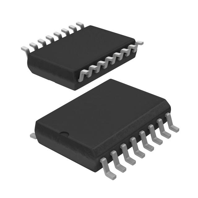


 工商网监
湘ICP备2023018690号
工商网监
湘ICP备2023018690号
